
Printed thick-film piezoelectric and pyroelectric sensors
Abstract:
The composition, structure and properties of piezoelectric and pyroelectric thick-films on ceramic and silicon substrates are surveyed. With particular focus on screen-printed films of ferroelectric ceramics in the family of lead zirconate titanate (PZT), applications in sensors and microsystems, actuators and energy harvesting are outlined and possible future trends delineated.
9.1 Introduction
The introduction of printed piezoelectric and pyroelectric films in the second half of the 1980s was an important step forward in the traditional thick-film technology (TFT), extending the choice of printable pastes beyond the most commonly available conductive, resistive and dielectric formulations used in hybrid microelectronic circuits. The times were ready for evaluation of the feasibility of new paste compositions for functional films that could replace more expensive crystalline materials, as well as polycrystalline ceramics less flexible to adapt in tailored shape and size.
The feasibility of screen-printed and fired piezoelectric thick-films based on the reported composition Pb0.9875[(Zr0.52Ti0.48)0.975Nb0.025]O3 was described in Fu et al. (1985), where the films were operated as acoustic transducers (buzzers). A similar application was apparently the motivation for the studies on BaTiO3-based thick-films in Philips Lab. Eindhoven (Baudry, 1987), whereas in Morten et al. (1989) the interest in lead zirconate titanate (PZT) films started to be oriented to sensors. All of these studies were carried out on films printed on alumina, and showed the potential of piezoelectric thick films for both actuators and sensors in terms of operating at lower voltages than bulk piezoelectric ceramics yet with satisfactory performances. Not less importantly, printed piezoelectric films advantageously offered flexibility in material composition and adequate miniaturization with patterning options for device layout, preserving mechanical robustness.
These promising characteristics soon determined an increasing interest for applications in micro-electromechanical systems (MEMS). In fact, printed films have thicknesses in the range from 10 to 100 μm, which offers the attractive perspective of producing microfabricated sensors, actuators and transducers without resorting to the impractical, difficult and expensive processes of thinning, machining and bonding bulk piezo-ceramics. This led to investigations on piezoelectric printed films in MEMS made by micromachining silicon, hereafter denoted as Si-MEMS, mostly employing PZT-based thick-films (Dorey and Whatmore, 2004).
Despite the issues faced, the results prompted a great deal of research into making PZT films compatible with silicon technology and developing applications in several areas with an emphasis on sensors. The past two decades have yielded an understanding of the reasons why piezoelectric thick films exhibit properties different from their ceramic counterparts, such as higher porosity and influence of clamping by the substrate. A better knowledge of procedures to obtain dense films and buffer layers as interdiffusion barriers has been achieved.
Significant research efforts have been also devoted to developing piezoelectric thick films on MEMS made with low-temperature co-fired ceramic (LTCC) technology, hereafter denoted as C-MEMS, which appear promising in a wide range of applications such as microsensors, microfluidic systems and miniature reactors. The first examples of piezoelectric Si- and C-MEMS are recently moving towards commercial availability for selected applications such as accelerometers (InSensor) and pressure sensors (Zarnik et al., 2009).
Thanks to the ferroelectric nature of PZT and the derived perovskites, PZT-based thick films also exhibit pyroelectric properties which have been studied since the 1990s, for instance in Leppävuori et al. (1995) and Lucat et al. (1997), and applied in visible and infrared radiation sensors.
An emerging field of investigation of piezoelectric and pyroelectric elements is in energy harvesting, i.e. the conversion from mechanical and thermal energy sources to the electrical domain in order to supply power for instance to sensors and microsystems, making them autonomous. PZT-based thick films are attracting significant attention in this field, again for their favorable properties and achievable thickness range.
In this scenario, the present chapter describes the use of screen-printed thick films to fabricate piezoelectric and pyroelectric devices. The chapter focuses on applications in sensors and microsystems. Material issues are treated only in those aspects, mostly related to technology, that are of interest to device designing. Processes for film deposition alternative to conventional screen printing, such as direct-writing techniques, are mentioned only briefly. Device and system issues in particular are covered, including transduction characteristics, modelling, impact on electronic signal readout, and examples of devices and their applications. Extensive reference to published literature is made, with the intention of providing a view on the state of the art in the field.
9.2 Piezoelectricity, pyroelectricity and ferroelectricity
Piezoelectricity, discovered in 1880 by the Curie brothers, is a property exhibited by a group of materials in which an imposed mechanical stress induces an electric charge/polarization (direct effect), and vice versa, an applied electric field develops a mechanical strain/deformation (converse effect) (ANSI/IEEE, 1987; Ikeda, 1989).
Piezoelectricity is a linear and reversible effect, i.e. polarization is proportional to strain and when the former changes from negative to positive or vice versa, then the latter also changes sign – unlike electrostriction, which is present in all dielectrics to various degrees, where the induced strain is proportional to the electric field squared.
The piezoelectric effect is exploited in a variety of applications that can be broadly grouped as sonic and ultrasonic wave generation and detection, and electromechanical or mechanoelectrical conversion. The former category comprises sensors and transducers, filters and resonators. The latter includes actuators and motors, nebulizers, transformers, gas igniters, energy harvesting generators, and more.
Pyroelectricity, named in 1824 by Brewster but known as a phenomenon since before that date, is the response of polar materials that display a spontaneous electrical polarization as a function of temperature, which results in the appearance of surface charges proportional to a temperature change ∆T (Lang, 2005; Whatmore, 1986). The polarization is along a unique axis called the polar axis.
Pyroelectricity finds applications in thermal radiation detectors (Muralt, 2001), i.e. those in which the incident radiation is indirectly converted into an electric signal by detecting the temperature increase due to the radiation absorption, unlike photon detectors, i.e. semiconductor-based quantum devices, where the radiant energy is directly converted into the electrical domain through the photovoltaic or photoconductive effects.
Pyroelectric detectors generally have a wide spectral response and require no cooling to improve the signal-to-noise ratio. Applications of pyroelectrics are in occupancy detection systems, contactless temperature measurement (pyrometers), infra-red cameras and vidicons, gas analysers, laser power meters, to cite a few.
In the piezoelectric and pyroelectric effects, steady inputs, i.e. constant stress and temperature, respectively, determine static polarization states in which the induced charges do not last indefinitely but are eventually neutralized by losses due to finite material resistivity. Therefore, in practice, only dynamic stress and time-varying temperature can be detected. This is often expressed by saying that piezoelelctric and pyroelectric sensors are AC-responding devices.
The origin of piezoelectric and pyroelectric behaviours in inorganic materials lies in the nature of the chemical bonding and the associated degree of structural symmetry (Damjanovic, 1998; Newnham, 2005), according to Fig. 9.1.

Out of the 32 crystal classes (point groups) into which crystals can be classified, 11 are centrosymmetric, therefore they posses no polar properties and are not piezoelectric nor pyroelectric. The remaining 21 classes are noncentrosymmetric, i.e. they lack a centre of symmetry, and 20 of them have asymmetries that lead to piezoelectricity.
Out of 20 such classes, 10 are spontaneously polarized, within a given temperature range, along a unique polar axis, therefore they are pyroelectric. Finally, a subclass of pyroelectrics in which polarization can be reoriented and reversed under an applied electric field is formed by the materials known as ferroelectrics. Ferroelectric materials generally exhibit strong piezoelectric and pyroelectric effects. Ferroelectrics can be either monocrystals, such as Rochelle salt or lithium niobate, or polycrystals, such as barium titanate or PZT ceramics (Haertling, 1999; Waanders, 1991).
In a ferroelectric material, spontaneous electric polarization depends on temperature and decreases upon heating. Above a certain temperature specific for the material, called the Curie temperature TC, the polarization vanishes and a phase transition occurs from the ferroelectric state to the higher-symmetry paraelectric state.
In ferroelectrics, no matter if crystalline or polycrystalline such as PZT ceramics, the electrical dipoles are arranged in different regions, called domains, each with homogeneous polarization. In an untreated material the domains are randomly oriented thus they average out and produce a zero net polarization. Therefore, even below TC, the presence of individual microscopic dipoles nevertheless results in the absence of significant macroscopic polarization.
To achieve a macroscopic polarization P, a process called poling is performed by applying an external electric field E, usually at a temperature higher than room temperature. Typically, the applied field is removed only when the material is again back at room temperature. The process is illustrated in Fig. 9.2.
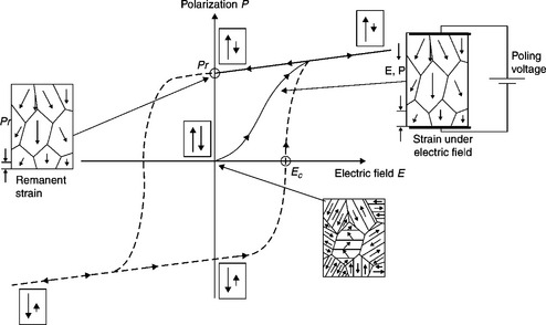
Starting from P = 0, where randomly oriented domains prevail, the external field E promotes their alignment in the field direction with a corresponding increase in P which tends to a maximum. When the field is removed, the material retains a remanent polarization Pr along the poling axis and thereby exhibits both the piezoelectric and pyroelectric effects. Domain orientation brings about an associated strain during poling, a fraction of which stays as remanent strain after the poling field has been removed. Poled ferroelectrics must operate at a temperature well below their TC, to contrast the tendency of structural transitions and thermal depoling.
If the applied field is changed in intensity and reversed at T < TC, domain switching can occur. In this case, the E–P plot describes a hysteresis loop where P becomes a two-valued function of E in the range between ± Ec, where Ec is defined the coercive field.
9.3 Basic theory and relationships of the piezoelectric effect
The interaction between the electrical and mechanical domains involved in piezoelectricity can be described by linear piezoelectric constitutive equations (Arnau, 2008; Ikeda, 1989).
There are different options for constitutive equations, depending on which of the electrical and mechanical quantities are chosen as the independent and dependent variables. In the monodimensional simplified hypothesis, the following four formulations are possible:
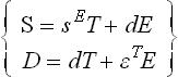
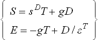
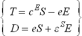
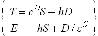
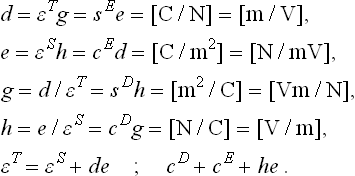
where S represents the strain [m/m], T the stress [N/m2], D the dielectric displacement [C/m2] that can be assimilated to polarization, E the electric field [V/m]. The coefficients sx, cx = 1/sx, and εx are respectively the elastic compliance [m2/N], elastic stiffness [N/m2] and dielectric permittivity [F/m], each considered for a constant value of the variable x. The terms d, e, g and h are called the piezoelectric constants. The first and second equations in the four pairs in Eqs. [9.1] describe the converse and direct effects, respectively.
The piezoelectric constants, elastic stiffness and compliance, and dielectric permittivity are linked as:
The energy transfer across the electrical and mechanical domains is expressed by the electromechanical coupling factor κ:
In the more general case of a tridimensional nonisotropic medium, the tensor notation becomes necessary for generalizing Eqs. [9.1] and to relate properties along different orientations of the material (Auld, 1973). The electric field and dielectric displacement are represented by three-dimensional vectors, while stress and strain, as second-rank symmetric tensors, can be represented by 3 × 3 matrices or six-dimensional vectors in the reduced-index Voigt notation.
The piezoelectric coefficients therefore become matrices where each entry has a pair of subscripts of which, in the conventional notation, the first one refers to the electrical direction (electric field or dielectric displacement) and the second one to the mechanical direction (stress or strain). For poled ferroelectrics, the axis 3 of a Cartesian reference frame is typically taken along the poling direction that usually is also parallel to the thickness of the sample or film. Therefore d33 describes the induced charge areal density on the surfaces of a film normal to the poling axis for unit stress applied along the same direction of poling. On the other hand, d31 describes the strain experienced by the film in a direction normal to the poling axis for unit electric field applied along the same poling direction.
For piezoelectric films the three-dimensional analysis is especially relevant in deriving the relationships between the material constants of the free element, e.g. an unclamped ceramic disk, and a film, thin or thick, adhering to a substrate. The difference between the two sets of constants is due to the clamping effect exercised by the substrate, which acts as a rigid base that affects the film behaviour both in the direct and converse piezoelectric effects (Damjanovic, 1998; Gwirc and Negreira, 2006; Lefki and Dormans, 1994; Muralt, 2008a; Torah et al., 2004). For example, the effective piezoelectric coefficients d33eff of a piezoelectric film on an isotropic substrate in the converse and direct effects, respectively, are related to the unconstrained coefficient d33 according to:
where νsub and Ysub are the Poisson’s ratio and Young’s modulus of the substrate, respectively. Considering the signs of the coefficients, d33eff results in both cases to be lower than the nominal d33 with reductions of 30 to 70%, which means that the films are significantly less piezoelectrically active than their free counterparts.
9.4 Thick-films based on ferroelectric inorganic compounds
Among the vast spectrum of interesting ferroelectric materials studied for their piezoelectric and pyroelectric properties (Heywang et al., 2008; Muralt, 2008b), PZTs are used in the majority of applications in thick-film based sensors, actuators and microsystems.
PZTs are polycrystalline solid solutions of two perovskite oxides, whose general formula is ABO3, namely lead zirconate (PbZrO3) and lead titanate (PbTiO3) in different relative amounts leading to Pb(ZrxTi1–x)O3, and they represent a family of materials with a Curie temperature TC around 250–350 °C, according to the Zr/Ti ratio (Ikeda, 1989). Above TC the structure is cubic, therefore, due to the associated symmetry, polar behaviour is precluded. Below TC the structure is asymmetric, either rhombohedral or tetragonal, hence the polar behaviour results. Attractive properties of PZT materials for sensing and actuating applications are the large piezoelectric and pyroelectric coefficients, high electromechanical coupling and the fairly high Curie temperature.
PZT powders are commercially available in various compositions with different grades and denominations, such as PZT-4, PZT-5, PZT-5H. Another commercial name of PZT is PXE, standing for piezoxide (Waanders, 1991). Small quantities of additives can be included to tailor the properties of the basic solution. A distinction is often made between ‘soft’ and ‘hard’ PZT compositions, which differ in the type of added dopants and the resulting macroscopic properties (Damjanovic, 1998).
Soft PZTs are characterized by high permittivity, high dielectric loss, large piezoelectric coefficients, high values of dielectric dissipation factors, and are easily poled but also more susceptible to depolarization. Hard PZTs have characteristics generally opposite to those of their soft counterparts, including low permittivity and dielectric losses, large mechanical quality factors, yet typically lower piezoelectric charge constants. They also are more difficult to polarize or depolarize.
PZT films can be advantageously deposited by screen printing as reported and reviewed in Baudry (1987), De Cicco et al. (1994a), V. Ferrari (2004), Fu et al. (1985) and Torah et al. (2007). Screen printing enables film thickness in the range from 10 to 100 μm using a sequence of a few printing/drying steps; on the contrary, less than 5 μm/layer is deposited with a typical sol-gel process. Such a comparatively high film thickness is often desirable for actuating and sensing purposes. Also, the film deposition process is simple, cost-effective and capable of defining feature sizes normally in the range of few hundred microns.
In typical PZT screen-printable pastes a PZT powder with average grain size in the micron range is used as the functional part. A PbO powder is often added (5 to 20% wt); it supplies an overpressure of Pb (or PbO) which, during the firing process at temperatures higher than 850 °C, counteracts the Pb volatilization from the active grains, compensates for the Pb lost in interactions with the substrate and acts like a sintering aid. A glass frit, e.g. a lead borosilicate, can be used as a binder to promote adhesion. Binderless PZT thick-films have also been studied (Cotton et al., 2007). As an organic vehicle to provide proper printability, a solution of in ethylcellulose terpineol leads to adequate rheology, but commercial thinners are used as well. Grinding of the powder mixture and wet ball-milling of the paste can be performed to improve homogeneity. The obtained PZT paste is then screen-printed on the substrate, which can be alumina (Al2O3), insulated metals, LTCC tapes or silicon.
For PZT layers in a planar sandwich configuration, the nature and composition of the bottom electrode, usually made by a thick-film conductor as well, may affect the properties of the overlaying layer, acting as a barrier to interactions between the film and the substrate. Lead diffusion from the PZT film into the substrate, either Si (Torah et al., 2007) or LTCC tapes (Belavič et al., 2009), may be a key issue in applications. The composition and deposition process for the top electrode on the fired films is much less critical. Screen-printed conductor layers or evaporated metal films are the most common solutions, while silver–polymer conductors have been used for characterizing the films and testing device prototypes.
After suitable drying and levelling steps, the printed layer is fired at a peak temperature in the range between 900 and 1000 °C for 20–30 min. Poling is then performed, typically under applied field of 2 to 5 MV/m at T ≥ 150 °C for about 30 min.
PZT thick-films differ from their bulk counterparts in density and grain size, as well as in elastic, dielectric and piezoelectric properties. For instance, the mass densities are about one-third lower while Young’s modulus, dielectric permittivity and piezoelectric coefficients can be several tens of percents lower in thick-films derived by the same powder than the ceramic material (Lou-Moeller et al., 2007). Such differences can be ascribed partially to the porosity of the films, found to span from 5 to even 60% according to the composition and process (Park et al., 2010; Walter et al., 2002), but the substrate clamping effect also plays an important role (Gwirc and Negreira, 2006).
To reduce the porosity and improve the overall characteristics of the films, a high isostatic pressure can be applied on the dried but yet unfired film (Hindrichsen et al., 2010a; Lucat et al., 1997; Yao and Zhu, 1998). In addition, sol infiltration of Pb(Zr1 − xTix)O3 can be used to reduce the porosity (Dauchy and Dorey, 2007; Park and Park, 2011).
Correlations among composition, processing, microstructural features and properties of PZT thick films have been analysed in Torah et al., (2005). Enhanced performances in screen-printed films obtained from a paste prepared with a mixed powder of both nano- and micro-sized piezoelectric particles without sol infiltration have been reported in Kwon et al. (2007).
A comparison of the properties of PZT thick-films with those of the ceramic counterparts made with the same PZT powder is reported in Table 9.1, which confronts the values extracted from the data sheets for thick-films from InSensor (www.insensor.com) and PZ26 hard-type bulk ceramic from Ferroperm (www.ferroperm-piezo.com).
Table 9.1
Comparison between the properties of screen-printed PZT thick-films from paste TF2100 by InSensor, taken from InSensor, and bulk ceramic of the same powder composition used for the paste, namely PZ26 hard-type from Ferroperm, taken from Ferroperm.
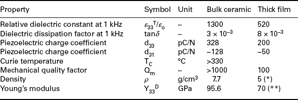
*Taken from Ferrari et al. (2001).
**Taken from Hindrichsen et al (2010a).
Currently, deviations from the ‘standard’ PZT thick-films described above are many. They include printed films on LTCC tapes for sensors and microsystems. The degradation of properties observed in films fired on LTCC, compared to the same compositions on Al2O3, are partially mitigated introducing proper interaction barriers (Belavič et al., 2007, 2009; Hrovat et al., 2003; Uršič et al., 2008). Also films directly printed on metals have been studied, including steel (Fu et al., 1985). In both cases, LTCC and metal, issues may arise from thermal expansion mismatch, a possible source of cracks (Dorey and Whatmore, 2004). Nevertheless, piezoelectric activity suitable for sensors and actuators has been obtained.
Attractive variants for the production of PZT thick films were studied, such as the use of binders that allow for low-temperature curing (Clegg et al., 1997; M. Ferrari et al., 2010a) and piezoelectric paints that can lead to films for coatings on plastics and flexible substrates (Egusa and Iwasawa, 1994; Payo and Hale, 2010). However, currently the properties exhibited by such low-curing temperature PZT compositions are poorer than those of conventional thick-films with typical values of d33 ranging in the order of magnitude of one-tenth of that of the parent compound.
A different matter is the deposition of piezoelectric films on silicon for MEMS. Screen printing has received significant attention despite the various issues encountered. Pb-Si interactions have been circumvented with adequate diffusion barriers to separate the silicon and lead-containing materials and to prevent the migration of atomic species with successful implementations in thin films and thick films as well (Chen et al., 1995; Dorey and Whatmore, 2004; Hindrichsen et al., 2010a; Gebhardt et al., 2007). Also, modified firing profiles have been studied to minimize the interactions and preserve film properties (Glynne-Jones et al., 2000), while set-ups were developed to print on thin fragile silicon membranes (Chapter 10).
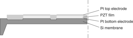
Nevertheless, current research is still ongoing to find deposition methods of thick PZT films on Si enabling improvements in performances and feature resolution at lower processing temperatures than thick-film technology. Investigations comprise aerosol (Wang et al., 2008), sol-gel spinning plus sol infiltration and photoresist-assisted pattern etching (Corkovic et al., 2007; Dauchy and Dorey, 2007; Frood et al., 2007), electrophoretic deposition and direct-writing techniques (Dorey and Whatmore, 2004). An example of low-curing temperature PZT films deposited on silicon MEMS is shown in Fig. 9.3 (Baù et al., 2011).
9.3 Example of low-curing temperature PZT films deposited by screen printing on a silicon MEMS cantilever after Baù et al. (2011).
9.5 Piezoelectric sensors
9.5.1 Modelling and configurations of piezoelectric transducers
If a piezoelectric prism of area A and thickness b is considered and harmonic regime at angular frequency ω is assumed, under the hypothesis that stress and strain do not depend on position along the thickness, the element behaves as mechanically concentrated. Under the mono-dimensional assumption, starting from Eq. [9.1c] and passing to the global variables tensile force F, outward displacement X, voltage V and current I, the equivalent electromechanical lumped-element model of Fig. 9.4 can be derived. The terms kE and CS represent mechanical stiffness at constant field and electrical capacitance at constant strain, respectively. This model is quasi static, being valid for frequencies lower than the first resonance of the piezoelectric element. Mechanical and electrical losses are not accounted for in the model. The circuits can be seen as the low-frequency limit of the Mason’s model corresponding to the same force applied at the two faces of the transducer (Mason, 1948).
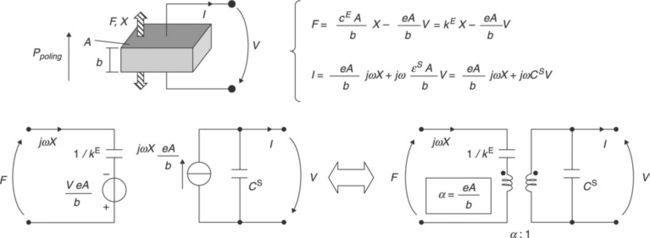
9.4 Equivalent circuit lumped-element model based on the electromechanical analogy at low frequency for a piezoelectric transducer under the mono-dimensional assumption.
The ideal DC-responding transformer with turn ratio α:1 represents the linear coupling between the electrical and mechanical domains. The electromechanical coupling factor κ can be derived from the model by reflecting the impedances through the transformer ports, leading to the following expression consistent with Eq. [9.3]:
While the transformer ratio α depends on dimensions, the electromechanical coupling factor κ is only related to specific material properties. Typical nominal values of κ for PZT ceramics range between 0.3 and 0.7.
Different types of piezoelectric transducers can be obtained depending on the configurations in which piezoelectric elements are arranged. Fig. 9.5 summarizes four general cases.
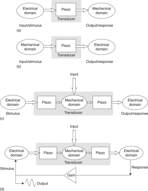
9.5 Configuration types of piezoelectric transducers: (a) electromechanical (EM) conversion; (b) mechanoelectrical (ME) conversion; (c) EMÐME conversion; (d) closed-loop EMÐME conversion.
Figure 9.5(a) shows the electromechanical (EM) conversion where the input signal is the electrical (E) stimulus to the piezoelectric element, and the output signal is the mechanical (M) response. In this configuration the piezoelectric element acts as an actuator. Examples of this type are micropositioners, motors, sonic or ultrasonic emitters.
Figure 9.5(b) represents the opposite case, where the input signal is the mechanical stimulus to the piezoelectric element and the output signal is the electrical response; this configuration gives a mechanoelectrical (ME) conversion and the piezoelectric transducer works as a sensor. Examples of this type are vibration pick-ups, sonic or ultrasonic receivers. When power, rather than current or voltage, is taken as the electrical output, the device is intended to perform mechanoelectrical energy conversion, such as in energy harvesting from mechanical vibrations.
Figure 9.5(c) represents a sensor configuration based on an EM–ME open loop conversion. An electrical stimulus to an input piezoelectric element generates a mechanical effect in a medium that is converted back into an electrical response by a second piezoelectric element. The input quantity, i.e. the one to be measured, modulates some property of the mechanical propagation path between the two piezoelectric elements, thus it is transduced into the output signal in the form of a perturbation of the electrical transfer function between stimulus and response. The mechanical propagation path can be external to the transducer or be an integral part of the transducer itself. In the latter case, the transducer sustains the propagation of mechanical elastic vibrations, i.e. acoustic waves, and the sensor can be referred to as an acoustic-wave (AW) sensor (Ballantine et al., 1997). The presence of two separate piezoelectric elements as input and output devices is not strictly required, since a single element can be used as well. In this case, the mechanoacoustic propagation path becomes the piezoelectric element itself.
Figure 9.5(d) extends the concept of acoustic-wave sensors by inserting the configuration of Fig. 9.5(c) as the feedback element of an amplifier, therefore creating an EM–ME closed-loop conversion. If proper gain conditions are satisfied, the system can be made resonating at one of the natural frequencies of the mechanoacoustic propagation path that, in turn, depends on the input measurand quantity. Therefore, the resonant frequency can be conveniently taken as the output signal. The resulting device is called an acoustic-wave resonant sensor (Benes et al., 1995; Hauptmann, 1991). AW resonant sensors offer a number of potential advantages such as high sensitivity, determined only by the mechanical properties of used materials and a response virtually unaffected by piezoelectric coefficients and amplifier gain. Good stability, resolution and high noise immunity are additional benefits, since the signal information is conveyed in the time scale rather than in the analogue amplitude. The ‘quasi digital’ nature of the frequency output facilitates the direct interfacing of resonant sensors to digital systems. Piezoelectric AW and resonant microsensors are comprehensively discussed in V. Ferrari and Lucklum (2008) and references therein.
9.5.2 Examples of devices and applications
Since the earliest investigations on piezoelectric printed films for buzzers (Fu et al., 1985), loudspeakers (Baudry, 1987) and developments thereof (Morten et al., 1989), piezoelectric films have been attracting a significant research interest for innovative applications in sensors and microsystems (Muralt, 2008b; Tadigadapa and Mateti, 2009).
Even limiting our attention to screen-printed films, the scenario of the investigated techniques and proposed devices is increasingly wide and diverse, with a growing tendency to migrate form traditional TFT substrates, such as alumina and possibly metal, to include silicon MEMS. This often implies deposition techniques and dimensional scales that are different from those of conventional screen printing, which in turn produces a range of ongoing developments and opportunities toward hybrid microfabrication technologies. For this reason, it was chosen to group the following examples according to the operating principles and configurations, as discussed in section 9.5.1, rather than divide them into technology categories, which are continuously evolving and increasingly interrelated.
A first implementation of an accelerometer (Morten et al., 1990) makes use of two piezoelectric films of 5 mm × 5 mm poled along the thickness, mounted back-to-back on the opposite sides of the seismic mass. Therefore the output results in a differential signal and the common-mode effects, such as temperature, are minimized. A flat frequency response between 0.5 and 500 Hz was observed, with a sensitivity of about 2.5 V/g for an acceleration range of ± 4 g and a temperature sensitivity of 3 × 10− 3 g/°C. The device proposed by Crescini et al. (2001) applies a similar structure. The sensor consists of two PZT layers, with a thickness of 40–50 μm each, screen-printed on the opposite sides of an alumina substrate and connected with opposite polarity to allow for thermal compensation. The sensor works without added seismic mass. A low-noise, large-bandwidth charge amplifier sets the low-frequency limit in the sub-hertz region. Experimental tests demonstrate a d33 coefficient of the PZT layers around 180 pC/N when poled at 3 MV/m, a sensitivity of the device of about 60 mV/g over the bandwidth 0.7 Hz–40 kHz, with a resolution of 0.025% of the full scale (FS).
The piezoelectric accelerometer described in Beeby et al. (2001) is one of the early examples of migration of PZT screen-printed sensors from alumina to micromachined silicon. It consists of a micromachined square seismic mass 2 mm × 2 mm suspended by four silicon 750 μm × 975 μm beams where PZT films are screen-printed. The sensor is equipped with a microprocessor circuit that provides self-validation by driving the piezoelectric elements and reading the resulting output.
Efforts to integrate screen-printed piezoelectric PZT thick-films with silicon technology have recently led to the micromachined high-bandwidth triaxial accelerometer described in Hindrichsen et al. (2010b). The microsensor has a square 1.2 mm × 1.2 mm seismic mass suspended on four 600 μm × 800 μm beams onto which 30 μm thick PZT films are screen-printed (Chapter 10). The tests demonstrate that voltage sensitivity is 0.31 mV/g in the vertical direction, 0.062 mV/g in the horizontal directions and the first mode resonance frequency is 11 kHz.
Pressure sensors based on PZT thick films and their evolution are a significant example of the flexibility of the technology and the capability to transfer different transduction principles into devices. Static pressure cannot be measured with piezoelectric elements, unless they are arranged in resonant sensor configurations as discussed in the examples presented later on in this section. Instead, dynamic pressure, or shock pressure waves, can be directly detected.
An example is the dynamic pressure sensor described in Crescini et al. (2002), which was designed for pressure peaks up to 100 MPa. The sensor consists of a 2 mm thick alumina substrate onto which a screen-printed PZT layer, 3 mm in diameter, is sandwiched between Pt-Au printed electrodes and poled through the thickness. The performance characteristics include a sensitivity of 80–110 pC/MPa, a linearity better than 2% FS in the range between 25 and 60 MPa, and a response time lower than 10 μs.
The use of PZT thick-films in slip sensors for the feedback control of prosthetic hands is illustrated in Cranny et al. (2005). Each stainless-steel fingertip of the hand, configured as a cantilever, is equipped with a sensor made by a poled PZT layer, about 100 μm thick, sandwiched between two gold electrodes overlapping over an area of 8 mm × 8 mm. The results of tests run with small masses dropped onto the surface of an inclined fingertip and allowed to slide over the top electrode indicate the potential of the sensor to detect the moment of first contact between the hand and an object, as well as its ability to detect the onset of slip.
A field of topical interest where piezoelectric thick films can be used as both sensors and actuators is in piezoelectric micromachined ultrasound transducers (pMUT). A typical requirement is to decrease dimensions of the single transducer to make compact arrays. At the same time, piezoelectric films of comparatively high thickness are necessary to generate and detect sufficient acoustic power. To this purpose, the combination of Si-MEMS technology with piezoelectric thick-films is attractive.
Arrays of pMUTs made by PZT films screen-printed on silicon are reported in Hirsch et al. (2005). As illustrated in Fig. 9.6, the configuration consists of a transducer matrix on top of a micromachined membrane. Since the PZT transducers were intended to operate as thickness-mode resonators instead of as actuators for the eigenfrequencies of the silicon membrane, they were designed so that there is no overlap between the resonance frequencies of PZT elements and membrane, respectively. A multi stage screen-printing process with firing at 950 °C allowed the creation of layers of PZT with a final thickness variable between 30 and 110 μm. In this latter case, a resonance peak at 4.9 MHz has been measured with a quality factor improvement over commercial bulk ceramics.
9.6 Cross-sectional diagram of piezoelectric micromachined ultrasound transducers (pMUT) made by PZT screen-printed on silicon membranes after Hirsch et al. (2005).
A two-dimensional pMUT array based on PZT films is described in Wang et al. (2006). The considered films range in thickness between 2 and 50 μm. It is recognised that they occupy a technological region between the processing capabilities of thin film and machining of bulk ceramics. To avoid the high firing temperature usually required for conventional thick-film pastes, a composite thick-film deposition technique is described. The process uses composite slurry consisting of a ceramic powder and an oxide ceramic producing sol. The composite slurry is then deposited using a spin coating process whereby the electroded substrate wafer is coated with the slurry spun at high speed to yield a thick film. The final thermal treatment is at 600 °C, which is lower than the conventional firing temperatures.
In the field of piezoelectric acoustic-wave and resonant sensors, one early example in TFT is the pressure sensor reported in Morten et al. (1992), which, thanks to the resonant principle, allows the measurement of static pressure. The sensor has a two-port resonator configuration based on an alumina circular diaphragm where an annular interdigitated actuator and a central sandwich sensor made by screen-printed PZT films are deposited. The diaphragm is excited in flexural resonance at its third vibration mode by properly applying feedback across the driving and reading PZT elements by means of a phase-locked loop (PLL) electronic circuit forming a pressure-controlled oscillator. The differential pressure applied across the diaphragm deforms it and generates a radial tension. This in turn increases the diaphragm equivalent stiffness, therefore the resonant frequency rises and the sensor is thus able to measure static pressure. The reported sensitivity is around 150 Hz/mmHg at a frequency of 57.8 kHz.
A hydrostatic pressure resonant sensor based on a rectangular alumina beam excited in flexural resonance by two PZT thick-film elements is described in V. Ferrari (2004). The beam was mounted in a dual-in-line (DIL) package supported by the bonding wires in an approximately free-free condition that provided a marked resonance at the fifth flexural mode located at 198 kHz. The hydrostatic pressure of a surrounding gas results in the increase of the beam inertia and the resonant frequency decreases accordingly. A linear behaviour up to 4 bar has been measured, with a sensitivity of around –35 Hz/bar in air. This sensor configuration has an extended measuring range and a high overload capability since no deformable diaphragms are present that may fracture. On the other hand, the sensitivity depends on the particular gas.
An intense activity on the development and applications of PZT printed films has been carried out at Fraunhofer Institute of Ceramics in Dresden (Gebhardt et al. (2004). Here the development of many sensors has also comprised piezoelectric resonant pressure sensors realized in LTCC technology (Partsch et al., 2003).
The Jožef Stefan Institute in Slovenia has also been very active in the development and applications of PZT thick-films. In particular, resonant pressure sensors with diaphragms less than 10 mm × 10 mm in size realized in LTCC technology for different pressure ranges in collaboration with HIPOT-RR are reported in Zarnik et al. (2009).
An early device relying on the acoustic-wave principle based on piezoelectric thick films was described in White and Ko (1993). A plate-wave sensor structure was realized on a rectangular alumina substrate using two screen-printed PZT elements with interdigitated electrodes working as emitter and receiver, respectively, of acoustic waves along the substrate. The sensor is configured as a two-port delay line that, equipped with an electronic amplifier, behaves as an oscillator. A constant force applied in the centre of the substrate generates a strain, which in turn produces a decrease in the frequency. A frequency decrement of around 40 Hz for a load of 100 g was reported at a resonant frequency of 8 MHz.
Similarly, acoustic waves launched and detected by two pairs of PZT thick films with interdigitated electrodes have been exploited to measure flow in a pipe as described in De Cicco et al. (1994b). The piezoelectric devices were realized on alumina substrates attached to the outside surface of a metal pipe where liquid flows. Flexural plate waves are generated by the PZT films through the substrates, and guided into the pipe. The wave patterns propagate in opposite directions, while their velocities result to be affected by the liquid flow in the pipe. Two different flow-meter designs have been studied, operating in the megahertz region and below 100 kHz, respectively. Both designs were provided with an oscillator, which synchronously drives the two guides at the same frequency. The change in phase difference between the piezoelectric signals induced in the two receivers, due to the change of the flow velocity, is taken as the sensor output. A flow sensitivity in water of 17 × 10− 2 deg/(mm/s) was measured for the second design over the range between 0 and 750 mm/s.
For the measurement of static force, Fig. 9.7 illustrates a PZT-on-steel resonant tuning fork sensor (Crescini et al., 1996). On a steel beam, a dielectric insulation layer was screen printed followed by three PZT thick films with associate electrodes. The two elements at the beam-ends connected in parallel work as a driver, and the central element as a sensor in a two-port configuration which, arranged in a feedback loop with an electronic amplifier, allows to excite the beam in flexural resonance. When the beam is clamped at both ends, an axial traction force increases the equivalent stiffness, therefore the resonant frequency rises. The relationship between frequency and applied force is linear for small forces. The beam was mounted on a clamped-free aluminium frame to transform an applied vertical force into beam strain. A sensitivity of 1.1 Hz/N at the resonant frequency of 35 kHz was measured, with a linear range reaching 800 N.
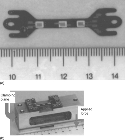
9.7 PZT-on-steel resonant tuning fork force sensor after Crescini et al. (1996): (a) picture of the fabricated sensor; (b) tuning fork sensor mounted on the supporting frame.
PZT thick-films allow the development of variable-mass AW sensors or, more generally, AW sensors responsive to an applied acoustic load (V. Ferrari and Lucklum, 2008). Variable-mass, also called gravimetric, AW sensors work as resonant microbalances. By functionalizing the surface with a sorption coating they can be used for chemical sensing.
PZT thick films were first used for gravimetric sensing in diaphragm and cantilever resonator sensors with polymeric coatings for the detection of humidity in air (Morten et al., 1993; V. Ferrari et al., 1996). A significant increase in mass sensitivity was later obtained by using the PZT thick-film resonator itself as the microbalance, leading to a device named resonant piezo-layer (RPL) sensor (V. Ferrari et al., 1997). As shown in Fig. 9.8(a), the structure of a thick-film RPL sensor is made by the superposition of a nonpiezoelectric substrate, specifically alumina, a bottom electrode layer, a PZT layer poled through its thickness and a top electrode layer. The PZT film is acoustically coupled to the substrate, leading to a thickness-expansion composite resonator, which can be used as a bulk acoustic wave sensor responsive to an acoustic surface load. Typical dimensions are 5 mm for the electrode diameter, and 250, 10 and 90 μm for the thickness of the substrate, electrodes and PZT, respectively. This results in a resonant frequency of around 7 MHz, while higher values can be achieved for thinner devices. A surface mass load on the top electrode determines a frequency decrement with a sensitivity higher than 500 Hz/μg at 7 MHz (V. Ferrari et al., 2001).
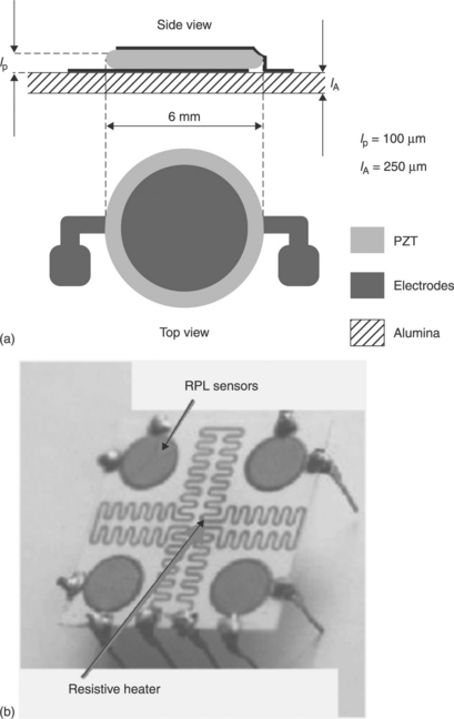
9.8 PZT-on-alumina resonant piezo-layer (RPL) sensor after V. Ferrari et al. (2000): (a) layout of the piezo-element; (b) array of four RPLs plus integrated resistive heater.
A multisensor array of RPLs on the same substrate is shown in Fig. 9.8(b). The array also integrates a resistive heater driven in the constant-temperature mode, to minimize the thermal drift of the sensor resonant frequencies that can typically be as high as 500–1000 Hz/°C.
By the use of proper sorption coatings, the achieved mass sensitivity was suitable for gravimetric chemical sensing (M. Ferrari et al., 2004; V. Ferrari et al., 2000). To further increase the mass sensitivity, it is desirable to reduce the sensor dimensions. As a significant example, silicon microcantilever resonators based on PZT thick films are described in Park et al. (2006). The thicknesses of the PZT and the silicon cantilever are approximately 22 μm and 12.3 μm, respectively. The reported estimated mass sensitivity for a 400 μm × 380 μm cantilever is nearly 32 kHz/μg at a resonant frequency of about 150 kHz.
A field of application of significant interest for piezoelectric materials is energy harvesting from mechanical sources, predominantly vibrations, to generate electrical supply for low-power sensor nodes (Kim et al., 2009). In this context, thick-film devices could provide solutions at an intermediate dimensional scale, which is conveniently lower than bulk devices yet retaining a sufficient volume to collect enough mechanical energy, as opposed to fully miniaturized devices whose power output inherently reduces due to decreasing size. A recent review of the potential of thick-films in the field of energy harvesting is given in Priya et al. (2009).
An energy harvester from vibrations based on PZT thick films on metal substrate is reported in M. Ferrari et al. (2010b). Vibration harvesters typically are linear mass-spring-damper systems working at resonance. Therefore, they are narrow-band devices whose conversion effectiveness falls if the frequency varies across a comparatively wide range. A different approach is here proposed based on nonlinear converters that exploit stochastic resonance to extract energy from broadband excitation.
As shown in Fig. 9.9(a), the converter consists of a piezoelectric film on an elastic beam coupled to permanent magnets to create a bistable system. Under proper conditions, the system bounces between two stable states in response to random excitation, which significantly improves energy harvesting from wide-spectrum vibrations. Nonlinear converters were realized by screen-printing low-curing-temperature PZT films on steel cantilevers equipped with magnets. Experimental tests were performed by measuring both the beam deflection and the output voltage under excitation by random vibrations at varying degrees of nonlinearity added to the system. Typical plots of the beam displacement and corresponding output voltage are shown in Fig. 9.9(b). The obtained results demonstrate an increase of up to 88% in the rms output voltage at parity of mechanical excitation when the system is made bistable.
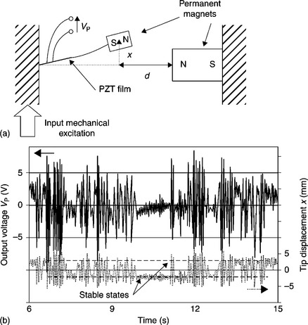
9.9 Nonlinear energy harvesting system formed by a piezoelectric cantilever beam and two permanent magnets after M. Ferrari et al. (2010b): (a) schematic diagram of the energy harvester; (b) harvester vibration displacement and output signal showing that when distance d is low enough, the cantilever bounces between two stable states.
The same principle can be implemented in a simplified single-magnet configuration that exploits the ferromagnetic properties of the elastic beam over which PZT thick films are screen printed (M. Ferrari et al., 2011).
9.6 Pyroelectric sensors
9.6.1 Basic theory and relationships of the pyroelectric effect
Pyroelectricity implies that the polarization P of a material is a function of temperature T. To avoid possible confusion with stress, in the present section temperature will be indicated with the symbol Θ.
In polar materials, P includes a spontaneous polarization PS in addition to the field-induced polarization P(E). In the scalar notation, the dielectric displacement D is therefore:
Assuming constant E, the derivative of D with respect to temperature Θ is:
The quantity pG is called the generalized pyroelectric coefficient of the material (Damjanovic, 1998). It can be observed that pG is made by two contributions: the first one, p = ∂PS/∂Θ, is the so-called true pyroelectric coefficient, while the second contribution represents the induced pyroelectric effect. Sensors exploiting the induced pyroelectric effect are said to operate in the dielectric bolometer mode. They do not require poling and are not limited to work below the Curie temperature of the material, but need an applied electric field (Muralt, 2001).
The pyroelectric coefficients are affected by the mechanical boundary conditions, i.e. whether the material is considered in clamped (constant strain S) or free (constant stress T) conditions (Liu and Long, 1978). Under constant strain, the so-called primary pyroelectric effect occurs. When the material is free to undergo thermal expansion, i.e. at constant stress, an additional contribution results from the piezoelectrically induced charge. This second phenomenon is sometimes called the secondary pyroelectric effect (Muralt, 2001).
The expressions of pG in the two cases can be derived by coupling Eq. [9.6] with the corresponding piezoelectric equations under either constant T or S, i.e. Eq. [9.1a] or Eq. [9.1c], respectively. This results in:
where α is the linear coefficient of thermal expansion and e is the piezoelectric constant. In the case of films on a substrate, the partially-clamped boundary conditions and the given materials determine the effective value of e, and thereof the relative importance of the primary and secondary pyroelectric effects (Damjanovic, 1998; Muralt, 2001).
Limiting our attention to the true pyroelectric effect expressed by the coefficient p, if electrodes are placed normal to P in a material where temperature Θ is assumed to be uniform and they are wired in a circuit, a time variation of Θ induces a current IP in the circuit, as shown in Fig. 9.10(a).
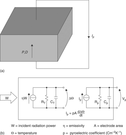
9.10 Pyroelectric sensor element: (a) simplified representation under short-circuit conditions; (b) electrothermal equivalent model under open-circuit conditions.
The electrical output can be related to the radiant energy input by means of the thermoelectrical equivalent model of Fig. 9.10 (b), where RT, RP and CT, CP represent the thermal and electrical resistances and capacitances, respectively. Assuming an incoming radiant power W harmonic at the angular frequency ω, the voltage and current responsivities are respectively defined as (Whatmore, 1986):
The dynamic properties of a pyroelectric sensor can be analysed by considering the frequency responses of voltage and current responsivities, and including the effect of the input preamplifier. To first order, a thermal and an electrical corner frequencies are present, respectively given by ωT = 1/RTCT and ωE = 1/RPCP. The relative positions of ωT and ωE depend on the material and geometrical parameters. For bulk materials generally ωE > ωT, whereas the opposite holds for thin films. The use of a transimpedance amplifier, due to its virtually zero input impedance, allows the tailoring of the electrical time constant by means of the external feedback components RF and CF, irrespective of RP and CP.
The simplified model of Fig. 9.10 becomes inadequate when the sensor has a multilayered structure and, therefore, the thermal profile along the thickness across the different materials is increasingly important (Samoilov and Yoon, 1998).
9.6.2 Examples of devices and applications
The reported pyroelectric coefficient p for PZT thick-films is typically between 1.2 and 1.5 × 10− 4Cm− 2 K− 1, depending on paste composition and poling parameters, while it is around 3.8 × 10− 4Cm− 2 K− 1 for PZT ceramics (Baudry and Delmas, 1991; De Cicco et al., 1999).
Densification promoted by the application of isostatic pressure before firing has been proposed to increase p (Lucat et al., 1997). Even though the pyroelectric coefficient of thick films is low, their reduced dielectric permittivity favourably determines a voltage responsivity that can be similar or higher than for bulk ceramics.
Pyroelectric sensors using PZT or modified-PZT screen-printed thick films have been reported as single-element detectors (De Cicco et al., 1999; Leppävuori et al., 1995; Lozinski et al., 1997), as well as in multisensor arrays (Baudry and Delmas, 1991; Lozinski et al., 1998).
In early works, measurements have been carried out mainly with relatively high-power light sources, such as lamps and lasers. For example, thick films of lead lanthanum zirconate titanate (PLZT) were used to fabricate a linear array that was tested under a flash lamp excitation (Lozinski et al., 1998). A pyroelectric detector made by a PZT thick film with buried electrodes was tested in response to an infrared (IR) chopped source with a peak power of 5.5 mW (De Cicco et al., 1999).
Multi-element thick-film pyroelectric sensors were also proposed for wide spectral range radiation detection (from IR to ultraviolet (UV)), and laser beam alignment and profiling. An array of 3 × 3 pixels (Capineri et al., 1998) and a four-quadrant detector (Capineri et al., 2004) made by PZT thick films on alumina intended for laser spot localization have been developed. The latter device is shown in Fig. 9.11 where the separation of the four quadrants obtained by sawing is visible.
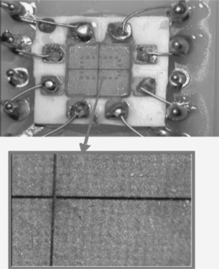
9.11 Pyroelectric four-quadrant detector after Capineri et al. (2004).
More recently, it has been demonstrated that the pyroelectric signals from PZT thick films can be detected even under excitation by low-power light sources, such as a light-emitting diode (LED) in the visible. If the LED is driven in amplitude modulation and the corresponding pyroelectric current is detected by synchronous demodulation, a DC signal is obtained which depends on the fraction of the LED light intensity impinging on the pyroelectric film. Interferences from thermal and light background are rejected. The maximum responsivity is typically obtained for a modulation frequency in the region around 100 Hz. The typical pyroelectric signal corresponds to peak temperature variations in the PZT film between 50 and 100 mK.
Based on this principle, pyroelectric contactless displacement sensors were proposed. As shown in Fig. 9.12, a pyroelectric film coupled to a LED can work respectively as the reference element and the movable light-spot cursor of a contactless linear displacement sensor (V. Ferrari et al., 2002). The sensor consists of a planar multi layer structure on alumina substrate where a rectangular film of PZT is enclosed between two PdAg electrode layers at the top and bottom. Each layer is in turn composed of a pair of triangular split electrodes (left, L, and right, R). The resulting four electrodes are combined in reverse-parallel with respect to the common poling direction, so that the pyroelectric signals from the R and L subsections subtract in a push-pull configuration producing a differential current. The LED spot position along the sensor length is converted into a suitably linear DC output by means of amplitude modulation of the LED and synchronous demodulation of the pyroelectric differential current. The readout method, combined with the differential configuration of the sensor, provides rejection of vibrations and microphonics caused by the piezoelectric response of PZT, as well as of external thermal and light sources. With a LED driving current of 33 mA at the stand-off distance of 3 mm, the measured sensitivity was 120 mV/mm over the range ± 10 mm, with a resolution better than 1.5 × 10− 3 of the span.
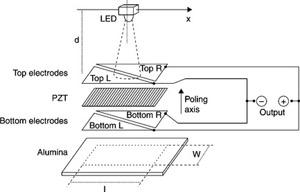
9.12 Contactless pyroelectric linear displacement sensor after V. Ferrari et al. (2002): sensor structure and operating principle with a LED cursor.
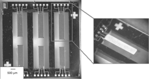
An extension of the same principle was proposed for biaxial position measurements by means of the pyroelectric sensor array shown in Fig. 9.13 (V. Ferrari et al., 2003). The sensor array is made by 8 × 8 pixels of PZT screen printed on an alumina substrate. The electrodes are configured as eight columns and eight rows evenly spaced, whose respective crossings form the 64 pixels of the array. As shown in Fig. 9.14(a), with an amplitude-modulated LED placed in front of the array and movable in the XY plane parallel to the array surface, the array and the LED respectively work as the reference element and the contactless cursor of a biaxial position sensor. A tailored readout and processing technique based on weighted amplification of the column and row pyroelectric signals produces a continuous and linear dependence of the output voltages on the XY position of the LED cursor. The measured sensitivity was 1 V/mm over the range ± 3.5 mm, with nonlinearity within ± 1% of the span. The resolution threshold was 4 μm, which is much better than the pixel pitch. Fig. 9.14(b) shows the results of biaxial measurements along the worst-case squared test path with side of 7 mm, i.e. on the borders of the linearity region. A good reconstruction of the LED trajectory can be observed.
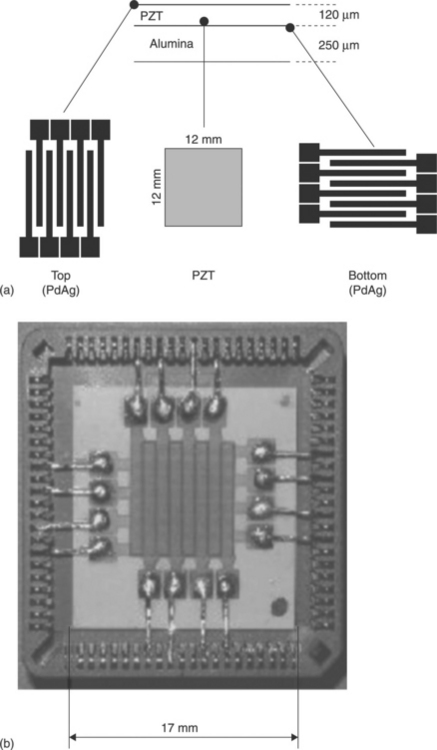
9.13 Pyroelectric array with 8 × 8 pixels for biaxial measurement of LED spot position after V. Ferrari et al. (2003): (a) array layout; (b) picture.
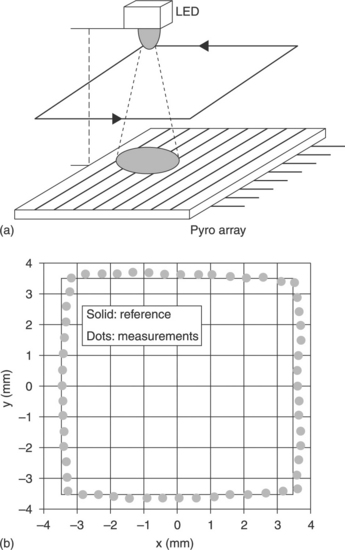
9.14 Characterization of the pyroelectric sensor array of Fig. 9.13: (a) test configuration; (b) measurement results along a square reference path.
Thick-film pyroelectric sensors for contactless displacement measurement offer low cost at large sensing areas when compared with semiconductor position-sensitive detectors. On the other hand, due to their limited frequency response with standard film and substrate thickness, they have been investigated for quasi-static applications so far.
Recently, the pyroelectric effect in PZT thick-films has started to be investigated for energy harvesting and possible use in generators for ultralow-power sensor modules. In Cuadras et al. (2010), PZT thick-films and commercial polyvinylidene fluoride (PVDF) elements were subject to thermal transients measuring currents and charges in the order of 10− 7 A and 10− 5 C, respectively, for temperature fluctuations from 300 to 360 K in a time period of the order of 100 s. Heating–cooling cycles were also investigated in order to accumulate energy. The pyroelectric current was rectified and the generated charge stored in a 1 μF capacitor up to an energy of 0.5 mJ.
In Dalola et al. (2010) sinusoidal temperature fluctuations were applied to screen-printed PZT films on alumina substrate. The charge extracted from the pyroelectric converter was stored into a capacitor using different rectifying circuits. The results of Fig. 9.15, where full-wave and voltage-doubler rectifiers are compared, show that after a few dozen heating–cooling cycles with a temperature rate of 1.8 °C/s, voltages in the order of 5 V and more are reached on a 10 μF capacitor in either case. The corresponding harvested energy can be compatible with use in autonomous sensors working in low duty cycle intermittent mode.
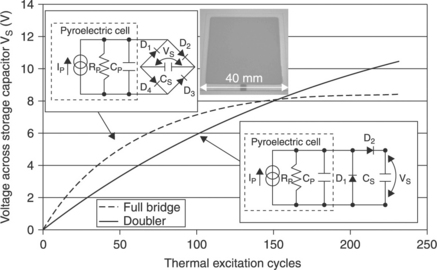
9.15 Pyroelectric elements on alumina used for thermal energy harvesting after Dalola et al. (2010): voltage across a 10 μF storage capacitor for different rectifiers with the sample, visible in the inset, excited with a sinusoidal temperature rate of 1.8 °C/s peak.
9.7 Future trends
In the field of piezoelectric and pyroelectric thick films, continuing research efforts are expected towards their integration with MEMS technology. While both silicon MEMS and electroceramics, in particular those with piezo- and pyroelectric properties, are successful technologies in their respective fields, their combination into devices amenable to manufacturing with repeatable and industrially-viable processes is still a matter of ongoing development. Piezo- and pyroelectric films of 10–100 μm thickness, such as obtainable by screen printing, can fill the gap between other deposition techniques and therefore will continue to be attractive. A large amount of technology and material aspects, applications and devices, including sensors and actuators, are comprehensively described in Setter (2005), which represents a valuable source of information and an overview on the current trends in electroceramic-based MEMS.
A key issue in the field of piezo- and pyroelectric devices is the requirement to progressively abandon PZT and look for lead-free materials. Due to the directive 2002/95/EC, commonly referred to as the Restriction of Hazardous Substances (RoHS) in the European Union and similar restrictions in other countries, the use of lead as well as other hazardous heavy metals is banned in the manufacture of electronic and electrical equipment. PZT typically contains a lead weight concentration around 60%, yet it has been granted a temporary exemption to RoHS, while the research for substitute materials has been encouraged (Rödel et al., 2009). Considerable research efforts by industry and academia are ongoing on the topic, but at present a one-to-one replacement for PZT is still not available (Panda, 2009). Barium titanate (BT), modified sodium potassium niobate (KNN) and bismuth sodium titanate (BNT) are examples of lead-free materials that have attracted significant attention. All of them show stable piezoelectric response providing comparable performances to PZT in some respects, but important limitations in others (Aksel and Jones, 2010). Therefore, the development of lead-free piezoelectric films of adequate performances for sensors and transducers will be a topic of interest in material science that will impact in device development (Setter, 2008).
Another topic that is expected to attract increasing research interest in the near future is the deposition, by screen printing or other methods, of thick films on nonconventional substrates such as plastics or textiles. The development of repeatable and cheap processes to obtain reliable sensors and interconnections on such diverse substrates is an ambitious goal that will bring advances in the broader research area of printed electronics. The timeliness of the topic is confirmed by recent projects funded by the EU such as, for example, 3Plast on printable, pyroelectrical and piezoelectrical large-area sensor technology (3Plast) and Microflex on micro fabrication production technology for MEMS on new emerging smart textiles/flexibles (Microflex).
9.8 Sources of further information
Consortium of academic and industrial researchers and end-users of energy harvesting (EH) technology: http://eh-network.org.
• IEEE Instrumentation and Measurement Society (IMS)
Society dedicated to research concerning the theory, methodology and practice of measurement, and in the design, development and evaluation of instrumentation and associated measurement systems: http://www.ieee-ims.org.
Council dedicated to research on the theory, design, fabrication, manufacturing and application of devices for sensing and transducing physical, chemical, and biological phenomena, with emphasis on the electronics, physics and reliability aspects of sensors and integrated sensor-actuators: http://www.ieee-sensors.org.
• IEEE Ultrasonics, Ferroelectrics and Frequency Control Society (UFFC-S)
Society dedicated to promote the advancement of the theory and practice of ultrasonics, ferroelectrics, frequency generation and control, and allied arts and sciences: http://www.ieee-uffc.org.
• International Microelectronics and Packaging Society (IMAPS)
Society dedicated to the advancement and growth of microelectronics and electronics packaging technologies through professional education: http://www.imaps.org/default.asp.
Consortium of academic and industrial researchers dedicated to the field of piezoelectric materials and devices: http://www.piezoinstitute.com
9.9 Acknowledgments
The valuable contribution of Professor Maria Prudenziati in enriching the scope of the chapter, and the helpful discussions and inspiring advice by Professor Andrea Taroni are gratefully acknowledged.
9.10 References
3Plast, Printable, Pyroelectrical and Piezoelectrical Large-Area Sensor Technology, EU-FP7 project. Available from: http://www.3plast-sensor.eu.
Aksel, E., Jones, J.L. Advances in lead-free piezoelectric materials for sensors and actuators. Sensors. 2010; 10:1935–1954.
ANSI/IEEE Std 176-1987IEEE Standard on Piezoelectricity. New York: Institute of Electrical and Electronic Engineers, 1987.
Arnau, A. Piezoelectric Transducers and Applications, 2. Berlin, Heidelberg: Springer-Verlag; 2008.
Auld, B.A. Acoustic Fields and Waves in Solids, 1–2. New York: John Wiley & Sons, 1973.
Ballantine, D.S., White, R.M., Martin, S.J., Ricco, A.J., Zellers, E.T., et al. Acoustic Wave Sensors. San Diego: Academic Press; 1997.
Baù, M., Ferrari, M., Tonoli, E., Ferrari, V., Sensors and energy harvesters based on piezoelectric thick-films. Procedia Engineering. Proceedings of Eurosensors XXV, Athens, Greece, September 4–7, 25. 2011:737–744.
Baudry, H. Screen printing piezoelectric devices. Hybrid Circuits. 1987; 14:71–74.
Baudry, H., Delmas, G., Thick-film pyroelectric sensor array. Proceedings of 8th European Hybrid Microelectronics Conference. 1991:227–235.
Beeby, S.P., Grabham, N.J., White, N.M. Microprecessor implemented self-validation of thick-film PZT/silicon accelerometer. Sensors and Actuators A. 2001; 92:168–174.
Belavič, D., Hrovat, M., Hole, J., Zarnik, S.M., Kosec, M., Pavlin, M. The application of thick-film technology in C-MEMS. Journal of Electroceramics. 2007; 19:363–368.
Belavič, D., Hrovat, M., Zarnik, M.S., Holc, J., Kosec, M. An investigation of thick PZT films for sensor applications: a case study with different electrode materials. Journal of Electroceramics. 2009; 23:1–5.
Benes, E., Gröschl, M., Burger, W., Schmid, M. Sensors based on piezoelectric resonators. Sensors and Actuators A. 1995; 48:1–21.
Capineri, L., Ferrari, V., Naldoni, F., Masotti, L., Marioli, D., et al. 3 × 3 matrix of thick-film pyroelectric transducers. Electronics Letters. 1998; 34:1486–1487.
Capineri, L., Casotti, L., Ferrari, V., Marioli, D., Taroni, A., et al. Comparisons between PZT and PVDF thick-films technologies in the design of low-cost pyroelectric sensors. Review of Scientific Instruments. 2004; 75:4906–4910.
Chen, H.D., Udayakumar, K.R., Cross, L.E., Bernstein, J.J., Niles, L.C. Dielectric, ferroelectric, and piezoelectric properties of lead zirconate titanate thick-films on silicon substrates. Journal of Applied Physics. 1995; 77:3349–3353.
Clegg, W.W., Jenkins, D.F.L., Cunningham, M.J. The preparation of piezoceramic polymer thick-films and their application as micromechanical actuators. Sensors and Actuators A. 1997; 58:173–177.
Corkovic, S., Zhang, Q., Whatmore, R.W. The investigation of key processing parameters in fabrication of Pb(ZrxTi1 − x)O3 thick-films for MEMS applications. Journal of Electroceramics. 2007; 19:295–301.
Cotton, D.P.J., Chappell, P.H., Cranny, A., White, N.M. A new binderless thick-film piezoelectric paste. Journal of Materials Science: Materials in Electronics. 2007; 8:1037–1044.
Cranny, A., Cotton, D.P.J., Chappell, P.H., Beeby, S.P., White, N.M. Thick-film force and slip sensors for a prosthetic hand. Sensors and Actuators A. 2005; 123–124:162–171.
Crescini, D., Ferrari, V., Marioli, D., Taroni, A. Thick-film resonant sensor for force measurement on stainless steel substrate. Sensors and Microsystems: Proceedings of the First National Conference on Sensors and Microsystems AISEM. World Scientific Publishing, Singapore, 1996.:256–260.
Crescini, D., Marioli, D., Sardini, E., Taroni, A. Large bandwidth and thermal compensated piezoelectric thick-film acceleration transducer. Sensors and Actuators A. 2001; 87:131–138.
Crescini, D., Marioli, D., Taroni, A., Romani, M. Development of high pressure sensors using PZT-based thick-films. Proceedings of 19th IEEE Intrumentation and Measurement Technology Conference, Anchorage, AK, USA, May 21–23. 2002:1555–1558.
Cuadras, A., Gasulla, M., Ferrari, V. Thermal energy harvesting through pyroelectricity. Sensors and Actuators A. 2010; 158:132–139.
Dalola, S., Ferrari, V., Marioli, D., Pyroelectric effect in PZT thick-films for thermal energy harvesting in low-power sensors. Procedia Engineering. Proceedings of Eurosensors XXIV, Linz, Austria, September 5–8, 5. 2010:685–688.
Damjanovic, D. Ferroelectric, dielectric and piezoelectric properties of ferroelectric thin films and ceramics. Reports on Progress in Physics. 1998; 61:1267–1324.
Dauchy, F., Dorey, R.A. Patterned crack-free PZT thick-films for micro-electromechanical system applications. International Journal of Advanced Manufacturing Technology. 2007; 33:86–94.
De Cicco, G., Morten, B., Prudenziati, M. Piezoelectric Thick-film Sensors. In: Prudenziati M., ed. Thick-film Sensors. Amsterdam: Elsevier; 1994:209–228.
De Cicco, G., Morten, B., Prudenziati, M. A flowmeter operating with plate waves induced by piezoelectric thick-films. Proceedings of IEEE Ultrasonics Symposium, Cannes, France, November 1–4. 1994:1327–1331.
De Cicco, G., Morten, B., Dalmonego, D., Prudenziati, M. Pyroelectricity of PZT-based thick-films. Sensors and Actuators A. 1999; 76:409–415.
Dorey, R.A., Whatmore, R.H. Electroceramic thick-film fabrication for MEMS. Journal of Electroceramics. 2004; 12:19–32.
Egusa, S., Iwasawa, N. Preparation of piezoelectric paints and application as vibration modal sensors. Journal of Intelligent Material Systems and Structures. 1994; 5:140–144.
Ferrari, M., Ferrari, V., Marioli, D., Taroni, A., Suman, M., et al. Cavitand-coated PZT resonant piezo-layer sensors: properties, structure, and comparison with QCM sensors at different temperatures under exposure to organic vapors. Sensors and Actuators B. 2004; 103:240–246.
Ferrari, M., Ferrari, V., Guizzetti, M., Marioli, D., Piezoelectric low-curing-temperature ink for sensors and power harvesting Part 2. Sensors and Microsystems Lecture Notes in Electrical Engineering. 54. Springer-Verlag, Berlin, Heidelberg, 2010.:77–81.
Ferrari, M., Ferrari, V., Guizzetti, M., Andò, B., Baglio, S., et al. Improved energy harvesting from wideband vibrations by nonlinear piezoelectric converters. Sensors and Actuators A. 2010; 162:425–431.
Ferrari, M., Baù, M., Guizzetti, M., Ferrari, V. A single-magnet nonlinear piezoelectric converter for enhanced energy harvesting from random vibrations. Sensors and Actuators A. 2011; 172:287–292.
Ferrari, V. Acoustic-wave piezoelectric and pyroelectric sensors based on PZT thick-films. In: Yurish S.Y., Gomes M.T.S.R., eds. Smart Sensors and MEMS. Dordtrecht: Kluwer Academic; 2004:125–154.
Ferrari, V., Lucklum, R. Overview of acoustic-wave microsensors. In: Arnau Vives A., ed. Piezoelectric Transducers and Applications. 2. Berlin, Heidelberg: Springer-Verlag; 2008:39–62.
Ferrari, V., Marioli, D., Taroni, A. Thick-film resonant piezo-layers as new gravimetric sensors. Measurement Science and Technology. 1997; 8:42–48.
Ferrari, V., Marioli, D., Taroni, A. Theory, modelling and characterization of PZT-on-alumina resonant piezo-layers as acoustic-wave mass sensors. Sensors and Actuators A. 2001; 92:182–190.
Ferrari, V., Marioli, D., Taroni, A. Displacement sensor based on pyroelectric thick-films and contactless light-spot cursor. IEEE Transactions on Instrumentation and Measurement. 2002; 51:819–823.
Ferrari, V., Marioli, D., Taroni, A., Ranucci, E. Multisensor array of mass microbalances for chemical detection based on resonant piezo-layers of screen-printed PZT. Sensors and Actuators B. 2000; 68(1–3):81–87.
Ferrari, V., Marioli, D., Taroni, A., Ranucci, E., Ferruti, P. Development and Application of Mass Sensors based on Flexural Resonances in Alumina Beams. IEEE Transactions on Ultrasonics, Ferroelectrics, and Frequency Control. 1996; 43:601–608.
Ferrari, V., Ghisla, A., Marioli, D., Taroni, A. Array of PZT pyroelectric thick–film sensors for contactless measurement of XY position. IEEE Sensors Journal. 2003; 3:212–217.
Ferroperm, Full Data Matrix, Ferroperm Matdata.xls. Available from: http://www.ferroperm–piezo.com
Frood, A.J.M., Beeby, S.P., Tudor, M.J., White, N.M. Photoresist patterned thick-film piezoelectric elements on silicon. Journal of Electroceramics. 2007; 19:327–331.
Fu, S.L., Chung, J.K., Cheng, S.Y. Properties and Applications of Screen-printed Piezoelectric Films. Japanese Journal of Applied Physics. 1985; 24(24-2):416–418.
Gebhardt, S., Partsch, U., Schönecker, A., PZT thick-fi lms for MEMS. Proceedings of 17th IEEE International Symposium on the Applications of Ferroelectrics, ISAF 2008; Santa Fe, NM, USA, February 23–28, 2008. 2004. [Article number 4693830].
Gebhardt, S., Seffner, L., Schlenkrich, F., Schönecker, A. PZT thick-films for sensor and actuator applications. Journal of the European Ceramic Society. 2007; 27:4177–4180.
Glynne-Jones, P., Beeby, S.P., Dargie, P., Papakostas, T., White, N.M. An investigation into the effect of modified firing profiles on the piezoelectric properties of thick-film PZT layers on silicon. Measurement Science and Technology. 2000; 11:526–531.
Gwirc, S.N., Negreira, C.A. Evaluation of the effect of porosity and substrate on the piezoelectric behavior of thick-film PZT elements. Journal of Physics D: Applied Physics. 2006; 39:4215–4221.
Haertling, G.H. Ferroelectric ceramics: history and technology. Journal of the American Ceramic Society. 1999; 82:797–818.
Hauptmann, P. Resonant sensors and applications. Sensors and Actuators A. 1991; 25–27:371–377.
Heywang, W., Lubitz, K., Wersing, W. Piezoelectricity Evolution and Future of a Technology. Berlin, Heidelberg: Springer-Verlag; 2008.
Hindrichsen, C.C., Lou-Møller, R., Hansen, K., Thomsen, E.V. Advantages of PZT thick-film for MEMS sensors. Sensors and Actuators A. 2010; 163:9–14.
Hindrichsen, C.C., Almind, N.S., Brodersen, S.H., Lou-Møller, R., Hansen, K., et al. Triaxial MEMS accelerometer with screen-printed PZT thick-film. Joutrnal of Electroceramics. 2010; 25:108–115.
Hirsch, S., Doerner, S., Salazar Velez, D.J., Lucklum, R., Schmidt, B., et al. Thick-film PZT transducers for silicon micro machined sensor arrays. Proceedings of IEEE Sensors 2005 Conference. 2005:444–447.
Hrovat, M., Holc, J., Drnovšek, S., Belavič, D., Bernard, J., et al. Characterization of PZT thick-films fired on LTCC substrates. Journal of Materials Science Letters. 2003; 22:1193–1195.
Ikeda, T. Fundamentals of Piezoelectricity. Oxford: Oxford University Press; 1989.
InSensor, TF2100 PZT thick-film based on Ferroperm Pz26, 1234182533.pdf. Available from: http://www.insensor.com
Kim, H.U., Lee, W.H., Rasika Dias, H.V., Priya, S. Piezoelectric microgenerators – current status and challenges. IEEE Transactions on Ultrasonics, Ferroelectrics, and Frequency Control. 2009; 56:1555–1568.
Kwon, T.Y., Kim, Y.B., Eom, K., Yoon, D.S., Lee, H.L., et al. Fabrication of stabilized piezoelectric thick-film for silicon-based MEMS device. Applied Physics A. 2007; 88:627–632.
Lang, S.B. Pyroelectricity: from ancient curiosity to modern imaging tool. August. Physics Today. 2005; 31–36.
Lefki, K., Dormans, G.J.M. Measurement of piezoelectric coefficients of ferroelectric thin films. Journal of Applied Physics. 1994; 76:1764–1767.
Leppävuori, S., Lozinski, A.H., Ussimäki, A. A thick-film pyroelectric PLZT ceramic sensor. Sensors and Actuators A. 1995; 46–47:391–394.
Liu, S.T., Long, D. Pyroelectric detectors and materials. Proceedings of IEEE. 1978; 66:14–26.
Lou-Moeller, R., Hindrichsen, C.C., Thamdrup, L.H., Bove, T., Ringgaard, E., et al. Screen-printed piezoceramic thick-films for miniaturised devices. Journal of Electroceramics. 2007; 19:333–338.
Lozinski, A., Wang, F., Ussimäki, A., Leppävuori, S. PLZT thick-films for pyroelectric sensors. Measurement Science and Technology. 1997; 8:33–37.
Lozinski, A., Wang, F., Ussimäki, A., Leppävuori, S. Thick-film pyroelectric linear array. Sensors and Actuators A. 1998; 68:290–293.
Lucat, C., Menil, F., Von Der Mühll, R. Thick-film densification for pyroelectric sensors. Measurement Science and Technology. 1997; 8:38–41.
Mason, W.P. Electromechanical Transducers and Wave Filters. New York: Van Nostrand Company; 1948.
Microflex, Micro Fabrication Production Technology for MEMS on New Emerging Smart Textiles/Flexibles, EU-FP7 project. Available from: http://microflex.ecs.soton.ac.uk
Morten, B., De Cicco, G., Prudenziati, M. Piezoelectric properties of PZT-thick-films. Proceedings of 7th European Hybrid Microelectronics Conference, Hamburg, FRG. 1989. [paper 8.4].
Morten, B., De Cicco, G., Prudenziati, M. Resonant pressure sensor based on piezoelectric properties of ferroelectric thick-films. Sensors and Actuators A. 1992; 31:153–158.
Morten, B., De Cicco, G., Prudenziati, M. A thick-film resonant sensor for humidity measurements. Sensors and Actuators A. 1993; 37–38:337–342.
Morten, B., Prudenziati, M., De Cicco, G., Alberigi Quaranta, A. Turin, Italy. Piezoelectric thick-film accelerometer for automotive applications. Proceedings of the 3rd Prometheus Workshop, 4. 1990:312–320.
Muralt, P. Micromachined infrared detectors based on pyroelectric thin films. Reports on Progress in Physics. 2001; 64:1339–1388.
Muralt, P., Piezoelectric films for innovations in the field of MEMS and biosensors 2008Heywang W., Lubitz K., Wersing W., eds. Piezoelectricity Evolution and Future of a Technology. Springer-Verlag: Berlin, Heidelberg, 2008:351–376.
Muralt, P. Recent progress in materials issues for piezoelectric MEMS. Journal of the American Ceramic Society. 2008; 91:1385–1396.
Newnham, R.E. Properties of Materials. New York: Oxford University Press; 2005.
Panda, P.K. Review: environmental friendly lead-free piezoelectric materials. Journal of Materials Science. 2009; 44:5049–5062.
Park, J.H., Park, H.H. In situ method of densification for powder-based piezoelectric thick-films for microelectromechanical system applications. Micro & Nano Letters. 2011; 6(9):749–754.
Park, J.H., Kim, H., Yoon, D.S., Kwang, S.Y., Lee, J., et al. Effects of the material properties on piezoelectric PZT thick-film micro cantilevers as sensors and self actuators. Journal of Electroceramics. 2010; 25:1–10.
Park, J.H., Kwon, T.Y., Kim, H.J., Kim, S.R., Yoon, D.S., et al. Resonance properties and mass sensitivity of monolithic microcantilever sensors actuated by piezoelectric PZT thick-film. Journal of Electroceramics. 2006; 17:565–572.
Partsch, U., Arndt, D., Keitel, U., Otschik, P. Piezoelectric pressure sensors in LTCC-Technology. Proceedings of European Microelectronic and Packaging Conference, Friderichshafen, Germany. 2003:331–335.
Payo, I., Hale, J.M. Dynamic characterization of piezoelectric paint sensors under biaxial strain. Sensors and Actuators A. 2010; 163:150–158.
Priya, S., Ryu, J., Park, C.S., Oliver, J., Choi, J.J., et al. Piezoelectric and magnetoelectric thick-films for fabricating power sources in wireless sensor nodes. Sensors. 2009; 9:6362–6384.
Rödel, J., Jo, W., Seifert, K.T.P., Anton, E.M., Granzow, T., et al. Perspective on the development of lead-free piezoceramics. Journal of the American Ceramic Society. 2009; 92(6):1153–1177.
Samoilov, V.B., Yoon, Y.S. Frequency response of multilayer pyroelectric sensors. IEEE Transactions on Ultrasonics, Ferroelectrics, and Frequency Control. 1998; 45:1246–1254.
Setter, N. Electroceramic-based MEMS: Fabrication-Technology and Applications. Berlin, Heidelberg: Springer-Verlag; 2005.
Setter, N. Trends in ferroelectric/piezoelectric ceramics. In: Heywang W., Lubitz K., Wersing W., eds. Piezoelectricity Evolution and Future of a Technology. Berlin, Heidelberg: Springer-Verlag; 2008:552–569.
Tadigadapa, S., Mateti, K. Piezoelectric MEMS sensors: state-of-the-art and perspectives. 092001. Measurement Science and Technology. 2009; 20:30.
Torah, R.N., Beeby, S.P., White, N.M. Experimental investigation into the effect of substrate clamping on the piezoelectric behaviour of thick-film PZT elements. Journal of Physics D Applied Physics. 2004; 37:1–5.
Torah, R., Beeby, S.P., White, N.M. An improved thick-film piezoelectric material by powder blending and enhanced processing parameters. IEEE Transactions on Ultrasonics, Ferroelectrics, and Frequency Control. 2005; 52:10–16.
Torah, R.N., Beeby, S.P., Tudor, M.J., White, N.M. Thick-film piezoceramics and devices. Journal of Electroceramics. 2007; 19:95–110.
Uršič, H., Hrovat, M., Belavič, D., Cilenšek, J., Drnovšek, S., et al. Microstructural and electrical characterisation of PZT thick-films on LTCC substrates. Journal of the European Ceramic Society. 2008; 28:1839–1844.
Waanders, J.W. Piezoelectric Ceramics. Eindhoven: Philips Components; 1991.
Walter, V., Delobelle, P., Le Moal, P., Joseph, E., Collet, M. A piezo-mechanical characterization of PZT thick-films screen-printed on alumina substrate. Sensors and Actuators A. 2002; 96:157–166.
Wang, X.Y., Lee, C.Y., Peng, C.J., Chen, P.Y., Chang, P.Z. A micrometer scale and low temperature PZT thick-film MEMS process utilizing an aerosol deposition method. Sensors and Actuators A. 2008; 143:469–474.
Wang, Z., Zhu, W., Miao, J., Zhu, H., Chao, C., et al. Micromachined thick-film piezoelectric ultrasonic transducer array. Sensors and Actuators A. 2006; 130–131:485–490.
Whatmore, R.W. Pyroelectric devices and materials. Reports on Progress in Physics. 1986; 49:1335–1386.
White, N.M., Ko, V.T.K. Thick-film acoustic wave sensor structure. Electronics Letters. 1993; 29:1807–1808.
Yao, K., Zhu, W. Improved preparation procedure and properties for a multilayer piezoelectric thick-film actuator. Sensors and Actuators A. 1998; 71:139–143.
Zarnik, S.M., Belavič, D., Maček, S., Hole, J. Feasibility study of a thick-film PZT resonant pressure sensor made on a prefired 3D LTCC structure. International Journal of Applied Ceramic Technology. 2009; 6(1):9–17.