
Printed varistors
Abstract:
Thick-film zinc oxide (ZnO)-based varistors have been prepared by screen-printing and tape-casting techniques. The manufacture of varistor thick-films by screen printing shows two critical problems: the excessive volatilization of Bi2O3 during the sintering step due to the exaggerated area–volume ratio of these devices and the lack of density of the green compacts, a problem inherent to screen-printing technology. Tape casting improves compact density and it is possible to include an additional press step before sintering. An electrical and microstructure comparison between thick-films prepared by both technologies has been carried out for a wide range of sintering temperatures. The excessive volatilization of Bi2O3 is overcome by sintering the films in a controlled Bi-rich sealed atmosphere, leading to high reliability and reproducibility in their nonlinear response.
17.1 Introduction
Zinc oxide-based varistors are multiphase ceramic devices prepared by sintering highly conductive n-type ZnO grains in the presence of a small amount of Bi2O3 and other metal oxides. Their nonlinear electrical characteristics, with excellent capability in applications for transient suppressions, were announced by Matsuoka et al. in 1969 [1] and further detailed in a topical 1971 paper [2]. General Electric (GE) acquired a licence for the related patents, and the joint development effort of GE and Matsuoka resulted in the market introduction of GE-MOV® varistors in 1972. This development has been one of the great successes of ceramic technologies. Presently, ceramic varistors are mass-produced in several countries, with applications ranging from power switching in electrical transmission lines to surge protection in automobiles and semiconductor electronics.
Recent interest in surface-mounted tape-casted and printed thick-film varistors (TFVs), especially in low-voltage circuits, has stemmed from the potential advantages of better integration, improved thermal exchange through the substrate and control of electrical properties [3,4]. Both tape casting and thick-films are well-developed technologies in microelectronics, benefiting from low cost, the possibility of miniaturization and design versatility among the recognised advantages. Nevertheless, the development of TFVs has so far posed notable problems. Their performance has suffered from the inadequate reproducibility of the electrical characteristics and a value of the nonlinear coefficient much lower than that of ceramic varistors.
This chapter describes ways in which printing technologies are contributing, and are expected to further contribute, to the realization of ‘low profile’ ZnO-based varistors.
17.2 The varistor action
ZnO-based ceramic varistors exhibit highly nonlinear current–voltage characteristics [6–13] that find widespread applications for circuit protection against voltage transients and power overload [7], from single electronic devices to power transmission lines.
An examination of varistor behaviour requires the display of current versus voltage on a logarithmic scale. Figure 17.1 gives the current density J versus the applied field F for a typical varistor, measured at a temperature near 300 K. In the standby situation (no spikes across) the varistor exhibits a high resistivity (ρ > 1012 Ω cm), i.e. it acts like an open circuit; but if the voltage across the terminals exceeds the critical breakdown voltage Vb, the varistor demonstrates a remarkable conductive behaviour (ρ < 1 Ω cm), so that the varistor is a short circuit for the current. The transition occurs in nanoseconds, is completely reversible, and is without hysteresis.
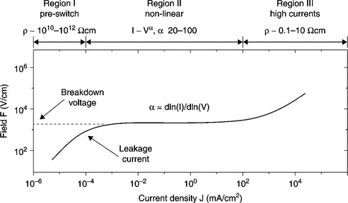
17.1 The current density J versus the applied field F for a typical varistor, measured at a temperature near 300 K.
It is a common practice to divide the I–V curve in three different regions, as shown in Fig. 17.1:
17.2.1 Region I (pre-switching or pre-breakdown)
In this region, where the varistor resistivity is higher than 1010 Ωcm, the current is denoted as ‘leakage current’; it determines the dissipated power by the varistor at standby and it is a notable function of the temperature [6]. High leakage currents imply an increase in temperature, due to the Joule effect, and consequently a degradation of the varistor performance. For practical reasons a reference leakage current is stated at a voltage equal to 85% of the breakdown voltage.
17.2.2 Region II (nonlinear, switching region)
In this region, i.e. starting from an applied voltage V across the terminals larger than the so-called breakdown voltage, there is an enormous variation in current (a factor of 103–105) despite the moderate change in the applied voltage V. A power law equation is conveniently used to describe this behaviour, that is:
where k is a constant that depends on the varistor dimensions. Hence α is derived from the experimental curve as α = dlog(I)/dlog(V). The higher the exponent α, the more efficient the varistor action is. In a ceramic varistor this is typically in the range 40–50.
17.2.3 Region III (high currents)
In this region, the deviation from the power law and the very high electrical currents can be interpreted as the existence of the ohmic series resistance associated with the oxide grains in the varistors.
Excellent reviews on different aspects of varistor ceramics are found in Clarke (1999) [5], Eda (1989) [14] and Gupta (1990) [15]. These papers point out the considerable technical and scientific efforts made to advance our understanding of the varistor action and improve their performance, because of the complexity of the physico-chemical phenomena involved. Even today there remain several points that require further investigation, e.g. the role played by the intrinsic defects and the ‘dopant oxides’ in the development of the microstructure and thus on their electrical behaviour.
However, the knowledge gained about ceramic varistors (hereafter also mentioned as bulk or disk varistors) is the natural background for the development of other forms of varistors, such as multilayer varistors (MLVs), surface-mounted tape-casted and printed TFVs [3,4]. Although both tape casting and thick-films are well-developed technologies in microelectronics, benefiting from the possibility of miniaturization, design versatility and low cost, the development of TFVs has posed notable problems so far. Their performance has suffered from inadequate reproducibility of the electrical characteristics and a value of the nonlinear coefficient α ~ 20 [16] that is much lower than in ceramic varistors (α ≥ 40). The origin of this poor behaviour is the excessive bismuth loss [17,18] during the sintering process, a loss that hampers the formation of a proper double Schottky barrier (DSB) at grain boundaries (GBs) [19–21]. In order to understand the role played by bismuth in the varistor action and thus the relevance of its loss in the varistor performance, it is appropriate to briefly summarise the main features of the varistor action.
Figure 17.2 shows the polished and chemically etched surface of a ZnO-based ceramic varistor: ZnO grains, a few micrometers in size, are adjoined by other crystalline phases, the most easily recognized being bi-reach compounds and the spinel ZnSb2O6.
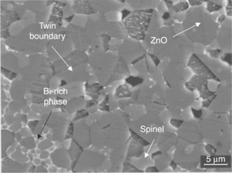
The overall microstructure can be described as ZnO grains isolated from each other by a three-dimensional series-parallel network of ZnO intergranular layers, responsible for charged GBs. The essential concept underlying the varistor action is that the J-V characteristics are controlled by potential barriers at these GBs arising from defects and dopants, which introduce electronic states in the energy gap and act as a trap for the charge carriers.
One such a barrier in thermal equilibrium is depicted in Fig. 17.3, where we observe the energy bands bending in two adjacent grains of the n-type semiconductor (ZnO).
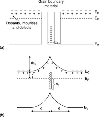
17.3 Energy bands bending in two adjacent grains of the n-type semiconductor (ZnO), (a) join of two semiconductor grains separated by an intermediate layer of grain boundary material and (b) formation of the double Shottky potential barrier.
Pure ZnO is a non-stoichiometric n-type semiconductor.
A sheet of trapped electrons at the boundary leaves behind a layer of positively charged donor sites on either side of the boundary, and creates an electrostatic field with a barrier at the boundary junction. Assuming an areal density, nt of trapped electrons and the charge carrier concentration in the grains of ND, the solution of the Poisson equation will give us the barrier height ϕB (V = 0) and the depletion layer width ö:
In the pre-switching region, the I-V characteristics (their ohmic behaviour and temperature dependence) fit very well a model of thermionic emission of electrons over these GB barriers, according to:
where A° is the Richardson constant, T the absolute temperature and k the Boltzmann constant.
The barrier height is thus dependent on the applied voltage and on the energy distribution of the trapping centers, as shown in Fig. 17.3, 17.4: V ≠ 0 shifts the local ‘quasi’ Fermi level and in turn results in a different concentration of trapped charges Qt.
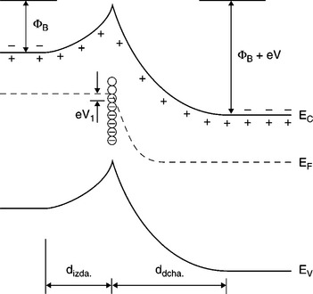
17.4 V ≠ 0 shifts the local ‘quasi’ Fermi level and in turn results in a different concentration of trapped charges Qt.
This DSB model is no longer adequate to describe the J-V curves in the switching region: another phenomenon occurs, namely under very high electric fields, some of the electrons crossing the barrier gain sufficient kinetic energy that they can produce minority carriers by impact ionization of the atoms within the depletion region. The minority carriers – holes – diffuse back to the GB under the influence of the electrostatic field at the boundary and compensate part of the trapped negative charge. In doing so, the potential barrier is lowered, thereby increasing the electron flow across the barrier. This ‘feedback’ process provides a high degree of nonlinearity in the electron transport in a manner similar (although not identical) to the ‘avalanche’ effect in Zener diodes [7].
A quantitative analysis of the model in line with these concepts shows that there is a critical doping level for a ZnO-based varistor, at about ND > 1017 cm− 3 to reach an electric field high enough for impact ionization. Analysis of experimental data shows that the typical values for the trap density, donor concentration and barrier height are Qi ~ − 1012 − 1013 cm2, ND ~ 1017 − 1018 cm− 3 and φ ~ 0.8 eV, respectively. With these values, the depletion width is ~ 0.1 μm, and the corresponding electric field in the vicinity of the GB is ~ 1 MV cm− 1 [1–10]. The corresponding breakdown voltage Vbo per barrier is typically in the range 3 to 3.5 V. The breakdown voltage Vb of the varistor body (thickness L) is proportional to the number of barriers between the electrodes and therefore inversely proportional to the average ZnO grain size d, according to:
[21]
17.3 Composition, preparation and microstructure of ceramic ZnO-based varistors
The varistor action has been observed in ZnO-based varistors containing bismuth, manganese and antimony oxides as minor components, as well as in simpler formulations containing only bismuth and manganese oxides and ZnO with bismuth Bi2O3 alone (although in the latter case the non-ohmic behaviour was far from high-performing, i.e. with α never larger than 10 [22,23]). Yet, the typical formulation of ZnO-based ceramic-type varistors comprises ZnO (> 95 mol %) and minor amounts of other metal oxides, such as Bi2O3, Sb2O3, Cr2O3, MnO2, NiO and CoO among others [24–29]. Current commercial varistors may contain as many as eight metal oxides or more.
The reason for this complex composition is related to the aim of optimizing all the properties requested for applications, such as stability, conduction uniformity, power dissipation, maximum surge current, energy dissipation capability, grain resistivity, and so forth, in addition to the nonlinearity exponent.
If the nonlinearity coefficient were the only important device parameter, with an acceptable low pre-breakdown current value, simpler compositions would be appropriate, e.g. those adding to ZnO, Bi2O3 and one or two more oxides of Co and/or Mn. Co and Mn are necessary to increase varistor nonlinearity [6,30]. These ions, in their divalent state, are known to go into solution in ZnO, but their valence state may change in the vicinity of a GB, especially with local changes in the oxygen potential; oxides of Ni [31] and Cr [32] are valuable for increasing the stability, while Sb2O3, which forms the spinel Zn7Sb2O12 phase segregated at the GBs, restrains the ZnO grain growth [33–34].
Other identified features are: (1) SnO2 shows a behaviour similar to that of Sb2O3 and, in addition, provides donors to ZnO [35]; (2) SiO2 contributes to stabilize the low temperature polymorphs of Bi2O3 [36–38] decreasing the leakage current as well as the grain growth; (3) Al2O3 contributes to the grain growth control and reduces the leakage current [39]; TiO2, BeO or Li2O [6] are also used to control the grain growth.
The close control of grain growth is vital to ‘define’ the breakdown voltage, according to Eq. [17.4]. Exaggerated grain growth could be a critical event during the sintering process. Here again, Bi2O3 plays a major role as shown below. In fact, Bi2O3 melts at 825 °C, but the first liquid phase is just formed at a lower temperature (~ 740 °C), i.e. at the eutectic point of the ZnO–Bi2O3 binary system [40–43]. The presence of the liquid phase favours matter transport and thus the densification of the material but it would also be responsible for exaggerated ZnO grain growth if a secondary phase, insoluble in the liquid, did not impede the GBs’ movement.
Usually ZnO varistors are fabricated via conventional ceramic powder processing methods to form a powder compact starting from ZnO and other oxides, which are weighed, mixed, dispersed and milled down to small size (e.g. 0.2–0.5 μm). The mixture is pressed into arbitrary forms, such as disks that are sintered in an electric furnace at 1150–1250 °C for 1–5 hours in air. The temperature is increased or decreased at low rates (e.g. 50–200 °C/hr). Finally electrodes are prepared on both surfaces.
In a simplified picture of the development of the microstructure and electrical properties from the compacted powders to the sintered solid body, the most critical recognized events are:
• The introduction of one/two liquid phases at relatively low temperatures: i.e. at 735 °C where the ZnO-Bi2O3 eutectic point is, and the melting at 525 °C of Sb2O5 formed by oxidation of the original Sb2O3.
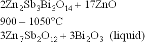
• The formation of the ZnSb2O6 solid (spinel) phase above 700 °C and secondary solids, including a pyrochlore 2Zn2Bi3Sb3O14(s) until about 950 °C.
• The further decomposition of the pyrochlore into the spinel and liquid Bi2O3 above 950 °C, accompanied by the dissolution of dopants to form Bi-rich liquids.
• In this high-temperature stage, the diffusion of dopants into the ZnO grains to provide a uniform dopant distribution and liquid-phase densification. Concurrently, grain growth occurs. The sintering temperature and time are chosen so as to optimize compositional uniformity, densification and grain size.
• In the following stage, during cooling down to intermediate temperatures, processes occur that include the crystallization of the secondary phases from the bismuth-rich liquid and the retraction of the liquid from two-GBs to the triple junctions. In this stage, potential barriers arise because in retracting from the two-grain junctions, the liquid leaves behind a segregation layer containing bismuth and other large ions. Details of the microstructure (barrier size, distribution of elements, oxidation states, etc.) depend mainly on how the varistor material is processed during cooling to room temperature.
• Also, the close control of the oxygen partial pressure is recognized as a mandatory requirement to obtain high-performance varistors [44,45].
Therefore, not only is the varistor action mostly due to Bi-rich phases at the ZnO GBs [24–29], but Bi is also involved in the main processes that lead to the development of the varistor microstructure.
17.4 Printing process in varistors fabrication
From the advent of surface-mount technology (SMT) it was advisable to design new forms of transient voltage suppression devices capable of meeting the new technological needs. The benefits in comparison with disk-shaped varistors were, among others: increased miniaturization and integration, low profiles, and drastic reduction of leads to minimize the inductive effects and thus reduce even further the overshoot voltage generated by fast-rising transients.
Both surface-mounted monolayer (SMV) and MLVs were introduced as a chip, that is, as discrete devices to be added to a board [3]. The multilayer technology has mostly progressed and devices from many manufacturers (e.g. Panasonic, Littelfuse, Cooper Bussmann, Epcos AG) with a wide range of characteristic parameters are today available. Conversely, pastes and processes for varistors to be directly deposited on the same substrate as a hybrid circuit – or embedded inside a low-temperature co-fired ceramic (LTCC) system – are still under development.
The issues arising in the transition from the ceramic to the thick-film technology come from three differences intrinsic to the latter one:
1. The amount of organic (medium) required to achieve the right rheology, with the accompanying effects, i.e. the change of chemical environment in the sintering (firing) atmospheres at low–medium temperatures, and the reduction in functional material density (intrinsic initial porosity).
2. The high area/volume ratio: surface effects are notably more influential in varistor layers a few tens of micrometers thick (the films) than in mm thick disks.
3. In typical thick-film processes, no pressure is applied to densify the dried paste before annealing. The exception (Ménil et al. [53]), mentioned below, remarks the importance of this step of process when related to TFVs.
The overall predominant effect of the listed features is that the loss of Bi via porosities and open spaces in general is enhanced in comparison to ceramic varistors, even though other effects cannot be excluded. In the case of MLVs, the processability of internal contacts with the varistor layers is a further issue.
The state of the art in the development of MLVs and the main steps in the progress of tape-casted and TFVs will be described in the following sections.
17.5 Multilayer varistors
The MLVs are formed by an alternate configuration of electrode layers and ZnO-based ceramic inner layers stacked together into a monolithic block, as depicted schematically in Fig. 17.5. This design greatly increases the available cross-sectional functional area, with the consequence of diverting transient over-voltages more effectively. This compact arrangement allows for higher resistances at lower voltages with faster response times than metal oxide varistors (MOVs), higher energy and heat dissipation. Breakdown voltage values span from a few (5 to 9 volts) to hundreds of volts [46–48]. However it is the low voltage range of applications that currently stimulates the manufacture of reliable MLVs.
17.5 Schematic showing how the MLVs are formed by an alternate configuration of electrode layers and ZnO-based ceramic inner-layers stacked together into a monolithic block.
The fabrication usually relies on the conventional multilayer ceramic technology. ZnO and other oxides are weighed, mixed, dispersed and milled down to a small size (e.g. 0.2–0.5 μm). Binders and plasticizers are mixed to obtain a slip to cast in green sheets using a doctor blade. A conductive paste is printed onto the green sheet to produce the inner electrodes. Next the printed sheets are stacked, laminated and cut into chips. Finally, free sintering or hot-pressing sintering under uniaxial pressure is conducted to densify these bricks. The outer contacts are then applied and cured.
Entering the field from the development of ceramic technology, a variety of new points have to be considered, including: (1) compatibility of inner electrodes with the varistor material; (2) grain growth conditioned by the space available between the inner electrodes [49]; (3) optimization of dielectric layer thickness and its homogeneity.
Platinum would be the metal of choice for inner electrodes, because it is inert with Bi2O3 -doped ZnO; however, it is too expensive for mass production. A possible candidate is 70 Ag/30Pd alloy, which however is known to interact with bismuth-based electroceramics [50] and to form Bi2PdO4 (in the temperature range 350 to 835 °C). This reaction can lead to profound changes in the MLV microstructure, according to the time/temperature sintering schedule. Moreover, the Bi2PdO4 decomposition (at T > 835 °C) is reportedly responsible for the possible delamination of multilayer stacks. On the other hand, attaining a homogeneous microstructure is necessary to control the electrical properties, since the electrical current tends to pass through the path with the smallest number of grains within inner electrodes; this ‘percolation’ effect can state the leakage current as well as the nonlinear coefficient α and the breakdown voltage. A successful strategy to accomplish homogeneous MLV microstructure is hot-pressing sintering in place of free sintering [51].
17.6 Screen-printed and fired thick-film varistors
Several authors have prepared low-voltage ZnO-based varistors by screen printing with and without glass in the composition. The glass phase was intended to accomplish denser and well-adhered layers on the substrate; however, the glassy phase is responsible for a marked change in microstructure and intergranular properties in comparison with those of bulk varistors and accordingly for very poor electrical properties, with nonlinear values of 8 and breakdown voltages of 15 V. Chiou and Jih [4] obtained breakdown voltages of 36 V and a nonlinear coefficient α of 16 with ‘screen-printed varistors in sandwich configuration’.
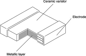
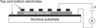
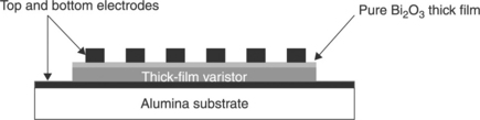
Governeur et al. [52] and Ménil et al. [53] proposed overcoming the drawbacks of porosity and short circuits observed in TFVs without glass by means of isostatic or uniaxial pressure of several Kilobars applied to the so-called wet film, i.e. after the evaporation of solvents and before the firing. This additional step to the standard screen-printing procedure results in a valuable expedient to reduce the porosity and prepare TFVs, sintered at 1150 °C with breakdown voltage of 30 V and α ∼ 15 with isostatically pressed samples and α in the range 17–19 in uniaxially pressed samples, respectively. Perrot [54] also studied uniaxially pressed screen-printed TFVs; he produced films with a good nonlinear coefficient (α = 12) but a breakdown voltage of 675 V, too high for the intended applications. Later, Martin [55] prepared varistors with planar configuration (Fig. 17.6) where the electrodes were screen-printed in parallel on top of the pressed pre-sintered varistor film.
17.6 Prepared varistors with planar confi guration where the electrodes were screen-printed in parallel on top of the pressed pre-sintered varistor film.
Therefore the measured properties were mostly due to the ‘near-surface’ section of the varistor rather that to the entire film. This configuration presents several advantages such as: the choice of conductive ink for the electrode is not affected by the sintering temperature of the varistor thick-films since the electrodes are fired after the sintering of the varistor itself. In this configuration, the possible reaction between the electrode ink and the active material is avoided during the sintering. On the other hand, this configuration only shows the electrical response of the surface and is not representative of the electrical response of the bulk material shaped like a thick-film. Such samples show a nonlinear coefficient α of 15 when sintered at 1150 °C/15 min. Hence, despite the certainly relevant Bi2O3 loss at this temperature [56], high-temperature sintering of pressed films is promising. Unfortunately it is difficult to state how much the configuration of the electrodes affected the measured quantities. In summary, the majority of TFVs studied until recently exhibited nonlinear coefficients α, between 10 and 20. The properties observed by Martin [55] were among the best (comparable with bulk varistors), notwithstanding that some doubt exists on the homogeneity of behaviour of their TFVs.
17.7 Progress in the development of ZnO-based thick-films and tape-casted varistors
The results described in this chapter refer to activities carried out for developing thick-film varistors at the Ceramic and Glass Institute (CSIC) from 2004 to 2006.
Samples discussed hereafter were prepared from powders of nominal composition: 95.5 mol% ZnO, 1.5 mol% Sb2O3, 1.0 mol%, Bi2O3, 0.5 mol% Co3O4, 0.4 mol% Cr2O3, 0.5 mol% Mn2O3 and 0.3 mol% NiO, Table 17.1.
Table 17.1
| Nomenclature | Ceramic powder processing |
| Powder 1 | Mixed oxides fired at 950 °C/1 h. |
| Powder 2 | Mixed oxides with the spinel phase Zn7Sb2O12 previously synthesized |
| Powder 3 | Mixed oxides with the spinel Zn7Sb2O12 and the sillenite Bi38ZnO58 phase previously synthesized. |
Three different pastes were prepared and designed:
1. Batch SCM: Prepared by the traditional mixed-oxide route including ball milling for 2 h in ethanol, calcination treatment at 950 °C–1 h and milling.
2. Batch SP: Traditional mixed-oxide route but replacing the Sb2O3 by the equivalent amount of a previously synthesized Zn7Sb2O12, an orthorhombic spinel phase.
3. Batch SP plus sillenite: As above, but replacing the Sb2O3 with the equivalent amount of Zn7Sb2O12 (orthorhombic spinel phase) and the Bi2O3 with Bi38ZnO58 (sillenite) phase, previously synthesized.
The average grain size of the starting powders was between 1 and 1.5 μm. The weighted oxides or compounds were mixed, dispersed and homogenized in a three-roller mill or in a planetary milling, with an appropriate vehicle. In order to achieve proper thixotropic properties (see Chapters 2–3) of the paste for the screen-printing process, the vehicle consists in α-terpineol, ethlyl-cellulose and [2-(2-butoxy-ethoxy-ethyl) acetate. Ethanol, ethylmethyl-ketone, polyvinylbuthyral, polyethylenglycol and benzylbuthylphtalate were used for the tape casting process. The amounts of mineral and organic phases were adjusted to match the rheological properties of the paste. Reference samples were prepared with the same compositions but the standard method of the ceramic technology, in order to compare and contrast microstructure and electrical behaviour.
17.7.1 Tape casting
In the tape-casting process, the paste is extended and levelled by knives on the substrate (doctor blade technique). The casting speed and the opening of the knives determine the thickness of the tape. Tape casting of the varistor ink was carried out on a commercial polymeric substrate (Mylar®) with 0.4 mm opening, producing tapes 70–90 μm thick after drying (30 °C). The dried films are cut according to the electroded substrate (2.5 × 5 cm) and both were pressed (0.6 Bar) together for 5–10 min at a temperature in the range 60 to 80 °C, i.e. close to the softening temperature of the substrate. Several tapes can be pressed in a single step. The firing cycles were carried out at 500 °C/2 h with heating and cooling rates of 0.2 and 1 °C/min [57]. Mylar is removed when the thick-film is dried at room temperature prior to the pressing process.
17.7.2 Screen-printed films
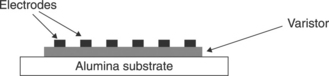
Dense alumina (96% Al2O3) was used for substrates because of its suitable properties, being a refractory, dielectric material with sufficiently high thermal conductivity. The pastes were screen-printed with a DEK 65 manual screen printer.
A Pt-based paste (Engelhard 6082) was printed on alumina and fired (850 °C/30 min) first. This film acts as the lower electrode for the varistor (screen-printed varistors in sandwich configuration) as well as a barrier to interaction between the alumina and the varistor element.
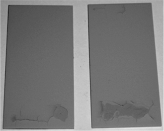
The ZnO-based paste was then printed, dried and sintered, varying the processing strategies with the intention to densify the varistors, avoid excessive Bi2O3 volatilization and control the ZnO grain growth. A single printed and fired varistor film is typically 10 μm thick. To accomplish thicker samples, 60–70 μm thick, free from cracks and electrical shorts and reproducible in electrical behaviour, up to six films were printed in sequence carrying out a drying step at 150 °C/15 min between each printing process. Next, thick-films are fired at 425 °C/0 h (i.e. without permanence at the peak temperature) with a heating rate of 0.5 °C and they dwell at 195, 270 and 385 °C for 30 min. Each thick-film is dried at 150 °C/15 min before screen printing the following thick-film, but the firing step to remove the organic additives from all of the films is carried out simultaneously before the sintering process. Figure 17.7 shows the surface of these fired samples.
It is obvious that the thermal processes to sinter and achieve the varistor action in printed or casted films cannot simply replicate those applied to bulk varistors, the main reasons being:
• The first step required is to burn out the organic vehicle. It has to proceed at a very low rate (0.1–0.5 °C) for complete elimination without cracks and sample distortions.
• A sintering process at high temperature over a long time, which should promote densification, also creates excessive Bi2O3 volatilization because of the unfavourable surface/volume ratio. Metz et al. [56] found that ZnO-based bulk varistors sintered at 1250 °C on alumina substrate had only 5% in weight remaining of the initial concentration of Bi2O3 and Peiteado et al. [58] measured losses of 60% in weight of initial Bi2O3 in high-voltage devices (bulk varistors). It is very important to take into account the fact that the area–volume ratio in thick-films is two orders higher than in bulk varistors and Bi2O3 volatilization is very much favoured and therefore it is easy to think that conventional sintering carried out in bulk varistors produces a complete loss of Bi2O3 in the thick-films. Therefore it is not easy obtaining ZnO-based varistors shaped as thick-films. These studies have confirmed that the Bi2O3 volatilization takes place from a Bi2O3-rich liquid phase formed from the decomposition of the pyrochlore according to:
17.7.3 Characterization of ZnO-based varistors
The electrical properties referred to in the following section were measured on printed and casted varistors with sizes of 1*2.5 cm, and thickness between 30 and 40 μm. Also data are shown consisting of three laminated layers of tape-casted samples of about 100 μm thick to increase the thickness of the film and have several grains between the electrodes. With three layers, the electrical response is more reproducible because there are more ZnO grains between the electrodes and therefore more GBs, which are responsible for the nonlinear behaviour. A series of sputtered Au dots uniformly distributed on the varistor was used to collect J-V curves in various regions of the sample and thus verify the homogeneity of its behaviour (Fig. 17.8).
The characteristic electrical parameters reported hereafter are: the breakdown voltage (Vc) measured at 0.3 mA/cm2, the leakage current (J) measured at V = 0.85 Vc and the nonlinear coefficient α measured between 1 and 10 mA/cm2. For comparative purposes, measurements were carried out on ceramic varistors prepared with powder SCM. These samples exhibited a nonlinear coefficient α of 50 when sintered in the temperature range from 1140–1180 °C for 2 h.
17.8 Microstructural and electrical characterization of ZnO-based varistors prepared by screen printing and tape casting
Tables 17.2, 17.3 and 17.4 show the nonlinear coefficient α measured on samples prepared with the three types of powders, fired at different peak temperatures (Tables 17.2 and 17.4) and at different dwell times (Table 17.3). Powder 3 shows an electrical behaviour similar to powder 2 although slightly poorer and therefore the following studies were carried out only with powders 1 and 2.
Table 17.2
The nonlinear coefficient a measured on samples prepared with the three types of powders, fired at different peak temperatures
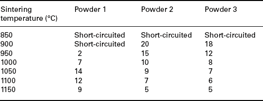
Table 17.3
The nonlinear coefficient α measured on samples prepared with the three types of powders, fired at different dwell times
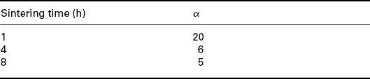
Table 17.4
The nonlinear coefficient α measured on samples prepared with powders 1 and 2, fired at different peak temperatures
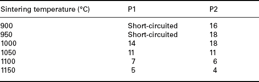
These results suggest that 900–950 °C is the most favourable peak temperature range for our samples, to avoid short circuits and attain reasonably high nonlinearity. The microstructure of the films fired in this temperature range is illustrated in Fig. 17.9 and 17.10.
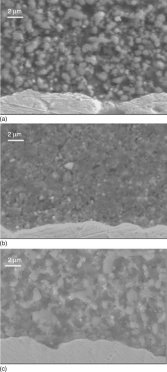
17.9 SEM micrographs of TFVs (top surfaces, not polished nor thermally or chemically etched) prepared from powders (a), (b) and (c) and sintered at 900 °C/1 h.
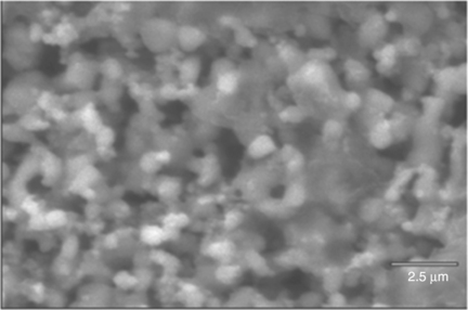
Figure 17.9 shows SEM micrographs of TFVs (top surfaces, not polished nor thermally or chemically etched) prepared from powders 1, 2 and 3 and sintered at 900 °C/1 h. Figure 17.10 is the SEM micrograph of a tape-casted layer sintered at 950 °C/1 h. In both cases (screen-printing and casting processes), grains in the size range of 2 to 4 micrometers are observed, showing that at these relatively low firing temperatures (900–950 °C), a limited grain growth occurred; the densification is likewise modest and accompanied by pores. On the other hand, Bi2O3 volatilization is not notable.
We can argue that the only contribution to the moderate grain growth was to a solid-state reaction or the low (about 750 °C) temperature when a first Bi-rich liquid phase was formed. At temperatures over 900–950 °C, the decline of α value is to be reasonably associated with increased Bi2O3 volatilization.
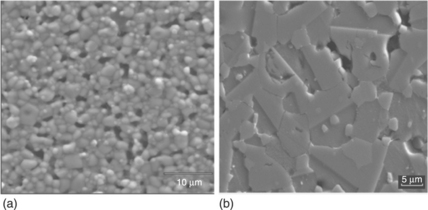
Figure 17.11 compares the microstructures of a screen-printed TFV and a bulk varistor, both sintered at 1000 °C. The difference in microstructure elucidates the difference in electrical response, α = 10 for thick-films and about 35 for bulk varistors. The thick-film still shows a Bi-rich liquid phase and the grain size essentially does not change in relation to the powders in the paste. On the contrary, the bulk varistor exhibits the characteristic microstructure with a homogeneous phase distribution of ~ 4 μm large ZnO grains, the spinel phase grains are distributed between the ZnO grains and in the triple points. It is important to point out that, at the same temperature, the microstructures of thick-films and bulk varistors are very different, and a consequence of this is their differing electrical response. The microstructural evolution is very different and this indicates that it is not as easy to achieve varistor thick-films with very good varistor properties using a starting powder that gives rise to very good nonlinear varistor properties when the material is shaped as a bulk varistor.
17.11 Comparison of the microstructures of a screen-printed TFV and a bulk varistor, both sintered at 1000 °C.
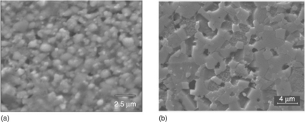
Figure 17.12 compares the microstructures of two types of our ZnO-based varistors. The one that was sintered in air with a conventional process exhibits the best electrical properties for its own class, i.e. the screen-printed film sintered at 900 °C/1 h (α = 20, E = 15 kV/cm, J = 1.2 mA/cm2 and the ceramic varistor sintered at 1180 °C/2 h (α = 48, E = 2.8 kV/cm, J = 0.035 mA/cm2). Both were prepared from the same powder, but show notable differences in grain size (less than 4 μm in the thick-film, and 7–8 μm for the disk), homogeneity (poor in the film) and appearance of the spinel phase (clear grey grains) located in the GBs in the ceramic sample, but not easily identified in the film. In addition to the microstructural differences, there are meaningful differences relating to the defects equilibrium in the interface or GB. The defects equilibrium reached at lower temperatures does not allow shaping of high potential barriers and, as a consequence, the nonlinear response is lower. High sintering temperatures are required since these temperatures favour the formation of the electronic defects needed for a suitable defects equilibrium (electronic states in the interface, cationic and anionic vacants, dopants, impurities, oxygen diffusion …) where the electrons are trapped, giving place to the Schottky barrier responsible for the nonlinear behaviour.
17.12 Comparation of the microstructures of two types of our ZnO-based varistors: (a) the screen-printed film that was sintered in air by a conventional process and exhibits the best electrical properties for its own class and (b) a bulk varistor.
A similar comparison is presented in Fig. 17.13 between a tape-casted layer and a bulk varistor, again taking the samples sintered in the conditions that offer the best characteristics in their own group. The tape is similar to the screen-printed film, having small grains, many pores attributed to Bi2O3 volatilization and poor densification.
Figures 17.14 and 17.15 show the J-V characteristics measured in screen-printed and tape-casted varistors, respectively, prepared with the various batches of powder described in Table 17.1. The results indicate that, in both cases (screen-printing and tape casting), powders 1 and 2 resulted in very similar behaviour. The best nonlinear coefficient value is never higher than 20 (Table 17.2).
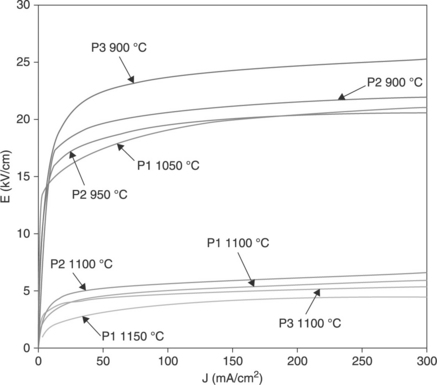
17.14 The J-V characteristics measured in screen-printed varistors prepared with the various batches of powder described in Table 17.1.
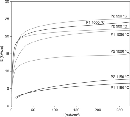
17.15 The J-V characteristics measured in tape-casted varistors prepared with the various batches of powder described in Table 17.1.
The only notable difference between the printed and cast samples concerns the fact that the latter exhibit electrical responses that are much less affected by the sintering temperature. The experiments always confirm that:
• Tape casting results in films with higher similarity in their electrical behaviour, despite variations in their sintering temperatures, associated with a higher similarity in microstructure.
• As expected, the higher the compact materials are, the higher the sintering temperature that is permitted before excessive loss of Bi2O3.
The varistor behaviour of the powders of the different batches, is reproducible always such as pressed samples of these batches (bulk). If the different processing steps are carried out in the same way, taking account of the following requirements of the raw materials, the obtained electrical response will be reproducible. However, it is necessary to use raw materials with high purity and small, homogeneous particle size of the ZnO and dopants raw materials. In the following ceramic processing steps (mixing oxide routes), it is necessary to carry out the processing in the same way without any variations. TFVs fabricated by screen printing show a reproducibility in electrical characterization of about 50% in the spots measured, due to the inherent porosity associated with this technique, and as a consequence of it, thick-films deposited by screen printing are less dense than the ones produced by tape casting. The reproducibility in the electrical behaviour of thick-films produced by tape casting reaches values around 90%. Almost all the electrical measurements carried out between the bottom electrode and different electrodes homogeneously distributed on the top surface of the thick-films show the same nonlinear behaviour. This result indicates that the microstructure is very homogeneous.
In short, all the attempts to improve the performance of our samples in terms of nonlinear coefficient and adequate microstructure were not successful when firing/sintering in standard ambient and standard conditions. Only when we started from powders of different batches were minor differences noted, and varistor action was only possible with peak temperatures below about 950 °C [58]. Therefore it was decided to approach the problem with various strategies aimed at limiting the bismuth loss from the samples, or at replacing the lost bismuth with new bismuth after the high-temperature process.
1. A Bi2O3 paste was screen-printed over the varistor thick-films previously printed (not sintered) on Pt/Alumina. The idea was to establish a quasi liquid-vapour equilibrium for Bi during the co-firing at high temperature (1150 °C) to prevent Bi2O3 vaporization from inside the film (Fig. 17.16). Regardless of the powder composition (P1–P3) and dwell times, no significant progress was obtained for the α-value (best results α = 19); on the contrary, the excess of liquid phase resulted in abnormal grain growth, a decrease in breakdown voltage and an increase in leakage current. The nonlinear behaviour improves if it is compared with thick-films sintered at high temperature without changes in the shaping of the films but the α value obtained is rather lower than in bulk varistors. α values of around 20 are obtained in thick-films without changes in the sintering process at low temperature (900 °C), but the final objective is to try to reach nonlinear coefficient values similar to those in bulk varistors (α ~ 40).
17.16 A quasi liquid-vapour equilibrium for Bi during the co-firing at high temperature (1150 °C) used to prevent Bi2 O3 vaporization from inside the film.
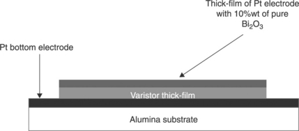
2. Firing the upper electrode, consisting of a paste of Pt enriched with Bi2O3, printed on top of the varistor layer. A platinum-based ink with 10%wt of Bi2O3 was printed on sintered varistor layers (Fig. 17.17). The film was then fired at 850 °C/30 min. The idea was to compensate, with the Bi2O3 in the conductive film, for the Bi2O3 lost during the sintering at high temperature. Yet, no significant progress in achieving high nonlinear coefficients was observed, regardless of the applied samples and sintering process.
According to Martin [55], this strategy resulted in ZnO-based TFVs with nonlinear coefficients α between 35 and 40, but they carried out the measurements of I-V between electrodes both located on top of the varistors. We can therefore guess that compensation for the Bi2O3 lost occurred near the varistor/electrode interface, whereas the Bi2O3 diffusion length in the already sintered varistor was too small to be efficient at larger distances.
3. Samples fired in a ‘closed’ space with Bi2O3 powder (Fig. 17.18).
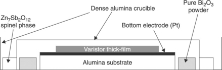
The idea is to ‘maintain a Bi-rich atmosphere’ around the sample. The spinel powder around the alumina ‘cover’ reacts with the Bi2O3 that is diffusing out (after this latter melts at 825 °C) to form a pyrochlore phase at temperatures between 700–900 °C. This compound ‘seals’ the alumina cover to the alumina crucible.
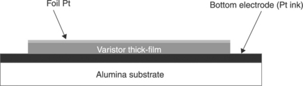
4. As in case (3), a closed space is created around the varistor, but with a Pt foil. The scope is to maintain in equilibrium the Bi2O3 in the vapour phase and in the liquid phase in the film (Fig. 17.19). Note that this experimental design would be unacceptable in industrial manufacturing processes due to the high price of Pt foils.
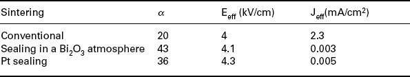
Data in Table 17.5 and Fig. 17.20 demonstrate the high effectiveness of strategies (3) and (4) above. Table 17.5 compares the electrical parameters of varistor tapes prepared with powder 1 and sintered in air or Bi-rich atmospheres. Figure 17.20 shows the corresponding J-V curves: the significant increase in the nonlinear coefficient is accompanied by a sharp transition from the pre-breakdown to the breakdown region, and by low leakage currents. Table 17.5 data correspond to three thick-films pressed and produced by tape casting and Table 17.2 data refer to one thick-film deposited by screen printing. The properties displayed by the tapes sintered in the Bi-rich atmosphere are close to those measured for a ceramic varistor sintered at a peak temperature of 1180 °C/2 h (α = 43, Jeff = 0.003, E = 4.1).
Table 17.5
Comparison of the electrical parameters of varistor tapes prepared with powder 1 and sintered in air or Bi-rich atmospheres
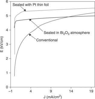
17.20 J-V curves corresponding to Table 17.5.
In Fig. 17.21, the nonlinear behaviour (I-V response) obtained for a ZnO bulk varistor and the ZnO thick-films is compared, with conventional sintering such as the films sintered with the changes carried out in the thermal treatment.
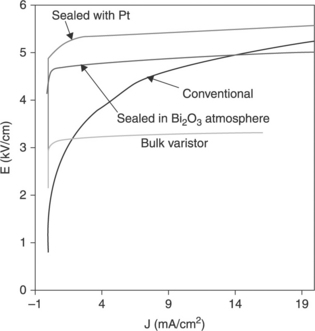
17.21 Comparison of the nonlinear behaviour (I-V response) obtained for a ZnO bulk varistor and the ZnO thick-films, with conventional sintering such as the films sintered with the changes carried out in the thermal treatment.
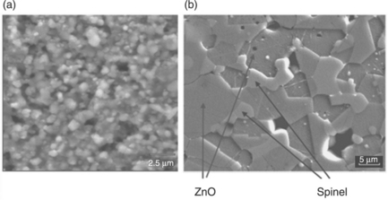
Figure 17.22 shows SEM micrographs of a bulk varistor sintered at 1180 °C/2 h in air with tape-cast layers sintered at 1150 °C/1 h under the conditions described above. Tapes are observed without polish or chemical attacks whereas the ceramic sample is polished and chemically attacked. The effect of sintering in a Bi2O3-rich atmosphere in terms of a limited loss of volatilized Bi2O3, and consequently in terms of grain growth, densification and homogeneous distribution of phases (including the spinel phase, brighter than the ZnO in Fig. 17.22) is quite evident. The grain size in sealed samples is comparable to that of a bulk varistor.
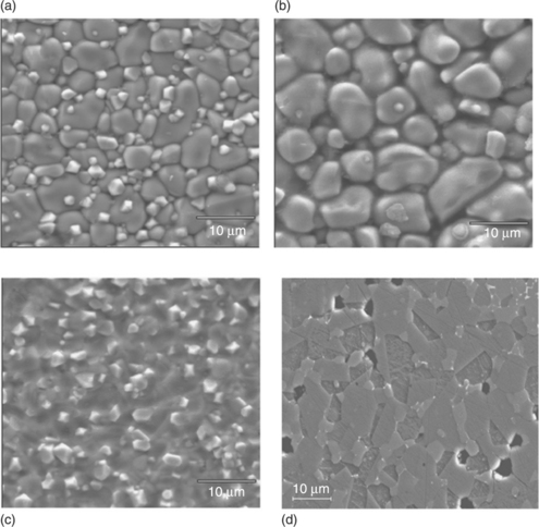
17.22 Comparison of the microstructures of tape-casted layers sintered at 1150 °C/1 h under different conditions and bulk ZnO-based varistors sintered at 1180 °C/2 h. (a) Layer sealed in a platinum foil. (b) Sintered in a Bi2O3-rich atmosphere. (c) Sintered in air (conventional). (d) Bulk varistor sintered in air. Layers are observed without polish or chemical attacks whereas the bulk ceramic sample is polished and chemically attacked.
17.9 Conclusion
Although much work is yet to be carried out to demonstrate the full potential of thick-film and tape-casting technologies in the development of film varistors, important steps in this direction have been accomplished. It has been shown that nonlinear coefficients α > 40 are accessible by ZnO-based film varistors sintered in a Bi2O3-rich atmosphere. Also, the other electrical characteristics tested approach those of ceramic ZnO-based varistors.
Further improvements might be reached by combining the approach of sintering in the presence of Bi2O3 powder in a near-closed space, with other expedients, such as pressures applied on wet films or layers, or a Bi-rich sol added to the oxide powders in the pastes.
Finally, we should not disregard approaches such as direct-write (ink-jet) deposition of new specially designed varistor inks, as this technology looks promising for varistor fabrication in the future [59].
17.10 Acknowledgements
Acknowledgements are to Dr. M. Peitedado, Dr. A. C. Caballero and Professor J. F. Fernandez of the Electroceramic Department of the Ceramic and Glass Institute (CSIC, Spain), Professor J. de Frutos of the ETSI Telecomunicación (UPM, Spain) and Professor M. Kosec of the Jozef Stefan Institute (Slovenia).
17.11 References
[1] Matsuoka, M., Masuyama, T., Iida, Y. Voltage nonlinearity of zinc oxide ceramics doped with alkali-earth metal oxide. Jpn J Appl Phys. 1969; 8:1275–1276.
[2] Matsuoka, M. Nonohmic properties of zinc oxide ceramics. Jpn J Appl Phys. 1971; 10(6):736–746.
[3] Puyané, R. Applications and product development in varistor technology. J Mat Proc Tech. 1995; 55(3–4):268–277.
[4] Chiou, B.-S., Jih, F.W. Studies on oxide-doped ZnO varistors with conventional pellet form and thick-film form. British Ceramic Proceedings. 1985; 36:129–141.
[5] Clarke, D.R. Varistor ceramics. J Am Ceram Soc. 1999; 82(3):485–502.
[6] Philipp, H.R., Levinson, L.M., Degradation phenomena in ZnO varistors: a reviewYan M.F., Heder A.H., eds. Additives and interfaces in electronic ceramics. Advances in Ceramics; vol. 7. Am Ceram Soc, Colombus, OH, 1983.:1–21.
[7] Blatter, G., Greuter, F. Electrical properties of grain boundaries in polycrystalline compound ceramics. Semicond Sci Technol. 1990; 5(1):111–137.
[8] Mukae, K., Electrical properties of grain boundaries in ceramic semiconductors Electrical properties of oxide materialsNowotny J., Sorrell C.C., eds. Key Engineering Materials. 125–126. Trans Tech Publications, Switzerland, 1997.:317–330.
[9] Levinson, L.M., Philipp, H.R. The physics of metal oxide varistors. J Appl Phys. 1975; 46:1332–1341.
[10] Eda, K. Conduction mechanism of nonohmic zinc oxide ceramics. J Appl Phys. 1978; 49:2964–2972.
[11] Mahan, G.D., Levinson, L.M., Philipp, H.R. Theory of conduction in ZnO varistors. J Appl Phys. 1979; 50(4):2799–2812.
[12] Morris, W.G. Physical properties of electrical barriers in varistors. J Vac Sci Technol. 1976; 13(4):926–931.
[13] Levine, J.O. Theory of varistor electrical properties. CRC Crit Rev Solid State Sci. 1975; 5:597–608.
[14] Eda, K. Matsushita Electric Industrial Co. Ltd., ‘Zinc oxide varistors’. IEEE Electrical Insulation Magazine. 1989; 5(6):28.
[15] Gupta, T.K. Application of zinc oxide varistors. 1990; 73(7):1817–1840.
[16] Bernasconi, J., Strassler, S., Knecht, B., Klein, H.P., Menth, A. Zinc oxide-based varistors: a possible mechanism. Solid State Commun. 1977; 21:867–870.
[17] Hower, P.L., Gupta, T.K. A barrier model for ZnO varistors. J Appl Phys. 1979; 50:4847–4855.
[18] Eizinger, R. Grain boundary phenomena in ZnO varistors. In: Leamy H.J., Pike G.E., Seager C.H., eds. Grain Boundaries in Semiconductors. New York: Elsevier; 1982:343–355.
[19] Pike, G.E., Semi-conducting polycrystalline ceramicsSwain, M.V., eds. Materials Science and Technology; Vol. 11. VCH, Weinheim, Germany, 1994.:731–754.
[20] Fernández Hevia, D., de Frutos, J., Caballero, A.C., Fernández, J.F. Mott–Schottky behaviour of strongly pinned barriers and characterization of ceramic varistors. J Appl Phys. 2002; 92(5):2890–2898.
[21] Tuller, H.L. ZnO grain boundaries: electrical activity and diffusion. J Electroceram. 1999; 4(S1):33–40.
[22] Tanaka, S., Akita, C., Ohashi, N., Hawai, J., Haneda, H., et al. Chemical state analysis of grain boundaries in ZnO varistors. J Solid State Chem. 1993; 105(1):36–43.
[23] Matsuoka, M. Nonohmic properties of zinc oxide ceramics. Jpn J Appl Phys. 1971; 10(6):736–746.
[24] Morris, W.G. Electrical properties of ZnO-Bi2O3 ceramics. J Am Ceram Soc. 1973; 56(7):360–364.
[25] Inada, M. Formation mechanism of nonohmic zinc oxide ceramics. Jpn J Appl Phys. 1980; 19(3):409–419.
[26] Wong, J. Sintering and varistor characteristics of ZnO-Bi2O 3 ceramics. J Appl Phys. 1980; 51(8):4453–4459.
[27] Takemura, T., Kobayashi, M., Takada, Y., Sato, K. Effects of bismuth sesquioxide on the characteristics of ZnO varistors. J Am Ceram Soc. 1986; 69(5):430–436.
[28] Olsson, E., Dunlop, G.L. The effect of Bi2O3 content on the microstructure and electrical properties of ZnO varistor materials. J Appl Phys. 1989; 66(9):4317–4324.
[29] Magnusson, K.O., Wiklund, S. Interface formation of Bi on ceramic ZnO: a simple model varistors grain boundary. J Appl phys. 1994; 76(11):7405–7409.
[30] Yodogawa, M., Yamakazi, T. The role of CO ions on the appearance of nonlinear I-V characteristics in ZnO based ceramics. J Electroceram. 1999; 4(S1):49–53.
[31] Asokan, T., Iyengar, G.N.K., Nagabhushana, G.R. Influence of additive oxides on the electrical characteristics of ZnO-based composites. Br Ceram Trans J. 1987; 86:190–193.
[32] Kim, T.H., Kawamura, H., Nawata, M. The effect of Cr2O3 additive on the electrical properties of ZnO varistor. J Mater Sci. 1997; 32:1665–1670.
[33] Senda, T., Bradt, R.C. Grain growth of zinc oxide during the sintering of zinc oxide-antimony oxide ceramics. J Am Ceram Soc. 1991; 74(6):1296–1302.
[34] Wu, L., Shen, C.Y., Chen, Y.C., Wei, Y.F., Chen, M.H., et al. The microstructure of ZnO varistor doped with antimony oxide. Jpn J Appl Phys. 1991; 30:2850–2856.
[35] Bernik, S., Daneu, N. Characteristics of SnO2 -doped ZnO-based varistor ceramics. J Eur Ceram Soc. 2001; 21:1879–1882.
[36] Levin, E.M., Roth, R.S. Polymorphism of bismuth sesquioxide II. Effect of oxide additions on the polymorphism of Bi2O3. J Res Natl Bur Stand: A Phys Chem. 1964; 68A(2):197–206.
[37] Shao, H.Q., Gao, X.H., Cao, Z.C. Effect of annealing on phase structure and degradation of a zinc oxide varistor with Si-additive. J Eur Ceram Soc. 1997; 17:55–59.
[38] Kutty, T.R.N., Ezhilvalavan, S. The role of silica in enhancing the nonlinearity coefficients by modifying the trap states of zinc oxide ceramic varistors. J Phys D: Appl Phys. 1996; 29:809–819.
[39] Tanahashi, M., Ito, M., Murao, M., Iga, A. Effect of Al-doping on the grain growth of ZnO. Jpn J Appl Phys. 1997; 36(Part 2–5A):573–576.
[40] Kimv, J., Kimura, T., Yamaguchi, T. Effect of bismuth oxide content on the sintering of zinc oxide. J Am Ceram Soc. 1989; 72(8):1541–1544.
[41] Senda, T., Bradt, R.C. Grain growth in sintered ZnO and ZnO-Bi2O3 ceramics. J Am Ceram Soc. 1990; 73(1):106–114.
[42] Dey, D., Bradt, R.C. Grain growth of ZnO during Bi2O3 liquid-phase sintering. J Am Ceram Soc. 1992; 75(9):2529–2534.
[43] Guha, J.P., Kunej, S., Suvorov, D. Phase equilibrium relations in the binary system Bi2O3-ZnO. J Mater Sci. 2004; 39:911–918.
[44] Stucki, F., Greuter, F. Key role of oxygen at zinc oxide varistor grain boundaries. Appl Phys Lett. 1990; 57(5):446–448.
[45] Bueno, P.R., Leite, E.R., Oliveira, M.M., Orlandi, M.O., Longo, E. Role of oxygen at the grain boundary of metal oxide varistors: a potential barrier formation mechanism. Appl Phys Lett. 2001; 79(1):48–50.
[46] Varistors: general technical information. Munich, Germany: Epcos AG Product Catalogue, 2002.
[47] Villegas, M. Multilayers ceramic materials. In: Fernández J.F., de Frutos J., eds. Introduction to Electroceramics. Madrid: Fundación Rogelio Segovia para el Desarrollo de las Telecomunicaciones, FUNDETEL, 2003.
[48] Rocak, D., Kosec, M., Degen, A. Ceramic suspension optimization using factorial design of experiments. J Eur Ceram Soc. 2002; 22:391–395.
[49] Kuo, S.-T., Tuan, W.-H., Lao, Y.-W., Wen, C.-K., Chen, H.-R. Inner electrodes for multilayer varistors. Int J Appl Ceram Technol. 2009; 6(2):223–230.
[50] Wang, F., Huebner, W. Interaction of silver/palladium electrodes with lead- and bismuth-based electroceramics. J Am Ceram Soc. 1993; 76(2):474–480.
[51] Lee, W.-H., Chen, W.-T., Hu, C.-L., Lee, Y.-C., Lin, S.-P., et al. Characterization of ZnO-based multilayer varistor sintered by hot-press sintering. Jpn J Appl Phys. 2006; 45(4A):2689–2694.
[52] Gouverneur, S., Lucat, C., Ménil, F., Aucouturier, J.L. New densification process of thick-film. IEEE Trans Compon Hybrids, Manuf Technol. 1993; 16:505–510.
[53] Ménil, F., Debeda, H., Lucat, C. Screen-printed thick-films: from materials to functional devices. J Eur Ceram Soc. 2005; 25(12):2105–2113.
[54] Perrot, F. doctoral thesis ‘The effects of multicurrent impulses on the low current bula distribution in varistor materials, under continuous AC operation’. UK: Brighton University; 1995.
[55] Martin, M.P. doctoral thesis ‘Realisation de varistances sérigraphies à base de ZnO pour des applications en électronique de puissance: influence des électrodes sur les propiétés électriques du composant de protection’. France: University of Bordeaux 1; 2003.
[56] Metz, R., Delalu, H., Vignalou, J.R., Achard, N., Elkhatib, E. Electrical properties of varistors in relation to their true bismuth composition after sintering. Mater Chem Phys. 2000; 63:157–162.
[57] Fernandez, J.F., Nieto, E., Moure, C., Duran, P., Newnham, R.E. Processing and microstructure of porous and dense PZT thick-films on Al 2O3. J Mater Sci. 1995; 30(21):5399–5404.
[58] Peiteado, M., de la Rubia, M.A., Velasco, M.J., Valle, F.J., Caballero, A.C. Bi2O3 vaporization from ZnO-based varistors. J Eur Ceram Soc. 2005; 25(9):1675–1680.
[59] Tohver, V., Morissette, S.L., Lewis, J.A., Tuttle, B.A., Voigt, J.A., et al. Direct-write fabrication of zinc oxide varistors. J Am Ceram Soc. 2002; 85(1):123–128.