
Chapter 3. Host Hardware Evolution
This chapter covers the following key topics:
 Advancements in Compute: Explains how the dramatic increase in processing power and the introduction of multicore CPUs make the server more powerful than the traditional storage controllers. Different terminology is covered, such as physical CPUs, virtual core, logical core, and virtual CPUs.
- Evolution in Host Bus Interconnect: Covers the introduction of fast speed buses such as the PCIe bus and the adoption of protocols such as NVMe that are well suited for handling much higher I/O bandwidth.
- Emergence of Flash-Based Products: Covers how the evolution in flash memory is getting cache speeds closer to traditional random access memory (RAM). A new generation of flash-based products is emerging on the host side and storage array side.
A major evolution in hardware has affected the data center. To start with, in compute alone, the latest CPUs for servers have more compute power than the legacy storage arrays that used to handle the input/output (I/O) load of all servers in an enterprise. Server interconnection to disks via Peripheral Component Interconnect express (PCIe) buses and the Non-Volatile Memory express (NVMe) protocol is dramatically increasing I/O bandwidth. The evolution of caching technology has created a new breed of all-flash arrays and high-performance servers. This chapter discusses this hardware evolution and how it affects the data center.
Advancements in Compute
You have heard of Moore’s Law, in which transistors per square inch on integrated circuits double year over year and will continue to do so for the foreseeable future. Central processing units (CPUs) are a perfect example. You have seen the quick CPU evolution on your PCs and laptops over the years. Listing the Intel processors alone could fill this page. The technology has evolved from a single-core CPU doing all the work, to multicore CPUs with clusters of CPUs sharing the load, to many-core CPUs offering larger and larger numbers of cores. The CPU performance, power savings, and scale have dramatically influenced the data center designs. Architectures that used to offload the CPUs with outside software controllers soon realized that the host CPU power exceeded the power of the controllers they were using. What used to be designed as an offload has fast become the bottleneck. A redesign is needed.
This chapter introduces you to some of the terms you hear when dealing with servers and compute to give you a better understanding of virtualization technology and how it uses such processing power.
x86 Standard Architecture
It is impossible to mention virtualization, convergence, hyperconvergence, and storage-defined storage without hearing the term x86 standard–based architecture. In fact, the whole movement behind software-based anything is to move away from “closed” hardware systems to standard-based x86. The irony is that many of the closed-based systems are also based on x86. The fact that the software in these systems is tied to the hardware makes them closed.
In any case, the term x86 standard architecture is mentioned a lot and deserves a brief definition. The x86 architecture is based on the Intel 8086 CPUs that were introduced in 1978. x86 is a family of instruction set architectures that has evolved over the years from 8-bit to 16-bit and then 32-bit processors. Many of the CPU architectures today from Intel and the other vendors are still based on this architecture. The x86 is the base for many hardware systems that will emerge in the years ahead.
Single-, Multi-, and Many-Cores CPUs
A core is the processing unit that receives instructions and performs mathematical and logical operations. The CPU, or the processor chip, has one core or multiple cores on it. Single-core CPUs were mainly used in the 1970s. The single-core CPU kept increasing in performance as companies such as Intel and AMD battled for the highest clock speeds. In the 2000s, the companies broke the 1 GHz clock speed barrier, and now they are breaking the 5 GHz barrier. Gaming had a lot to do with this because the complexity and speed in video games kept increasing. Long gone are the days of kids being happy with playing Atari Pong video games (1972).
As the single-core processor speed increased, heat and power consumption increased, challenging the physics of single core. Then followed the creation of dual-core processors, which began emerging in the 2004–2005 timeframe. A dual-core CPU had two cores on the same die. (A die is the circuitry that sits on a little square in a wafer, which is a thin slice of semiconductor material.) From the single core, the number of cores increased to 2, 4, 6, 8, and so on. Figure 3-1 shows the difference between a single CPU, single core and a dual CPU multicore. Just to be clear about the terminology, the CPU is the central processing unit chip that contains the bus interfaces and the L2 cache, whereas the core contains the register file and the L1/L2 cache and the arithmetic logic unit (ALU). The cache in the CPU and core allows for faster access to data than getting it from the RAM. Notice in this book that the RAM and solid-state drives (SSDs) are also used as L1/L2 caches for faster access to the data. The socket is the connector on the motherboard that forms the contact between the motherboard and the CPU.
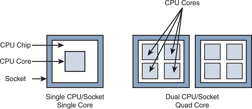
Note that dual core is different from dual CPU or dual socket. Every socket has one CPU, so dual socket and dual CPU mean the same thing. A dual core or a quad core means that the CPU has in it two cores or four cores. This might seem basic to many people, but confusion arises when physical cores and virtual cores are discussed.
Physical Cores Versus Virtual Cores Versus Logical Cores
You might hear the terms physical, virtual, and logical cores. A physical core is actually what it says: a physical core on a die that sits on the CPU chip. A technology called hyperthreading (HT) began emerging, in which the same core processes multiple threads at the same time. Hyperthreading helps in applications that support multiple threads. A core that supports hyperthreading, say two threads, is thought to have performance similar to two cores. This is not actually true. Hyperthreading allows a single core to work better by taking advantage of any idle time to run the second thread. So this, of course, gives performance improvements, but nothing close to having physical cores. A single-core CPU with two threads does not perform as well as a two-core CPU. In essence, when a manufacturer advertises an eight-core CPU with multithreading, it could mean four physical cores and four virtual ones. The virtual core is the extra thread that you get from hyperthreading.
The number of logical cores is the total number of physical cores and virtual cores. Here’s an example. A six-core CPU with hyperthreading results in twelve logical cores: six physical cores plus six virtual cores. In a VMware vSphere environment, a physical CPU (pCPU) refers to a single physical CPU core with no hyperthreading or (just for added confusion) to a single logical CPU core when hyperthreading is turned on.
Be sure that the application actually can use hyperthreading to leverage the virtual cores. If an application is designed to run multiple threads, then turning on virtual cores results in improved performance; if not, then virtual cores do not add value.
In addition to the number of cores in the CPU, vendors are incrementing the number of memory channels that connect the CPU to the RAM and are increasing the number of I/O buses that connect to storage. Some implementations have reached 32 cores per CPU and dual CPUs per server, reaching 64 physical cores or 128 logical cores with hyperthreading. Also, the number of memory channels has reached 16 per dual CPU, and the number of I/O lanes has reached 128. These numbers keep increasing, making the servers more powerful than ever.
Virtual CPU
A virtual CPU, not to be confused with a virtual core, is an actual slice of a core. Let’s rewind a bit. The physical processor may have one or more cores, and each core can be considered many smaller processing units called virtual CPU (vCPU). The concept of vCPU is used with virtualization, in which the hypervisor allocates a certain number of vCPUs to a virtual machine (VM). The question that is asked the most is how many vCPUs you can have per VM and how many VMs you can run per host. The answer to the first question is easy, mainly because the virtualization software itself, like VMware, does not allow you to exceed certain limits. So in VMware, if you have eight logical cores (four physical and four virtual via hyperthreading), the maximum you can have is eight vCPUs (one vCPU per logical core). What is recommended normally is to have one vCPU per physical core because HT cores give a performance boost for the same core, but they are not actually separate cores.
The bottom line is that you have so many physical cores to work with, you have hyperthreading to make sure these cores do not sit idle, and you have cache and RAM, where you swap information to and from. Starting from these limits, you have to give your applications what they need, not more and not less. So, if an application recommends using two vCPUs and you give it four vCPUs, there is a good chance that the application will have worse performance. This is due to CPU scheduling and fair allocation of tasks. The following is an oversimplification of CPU allocation and memory allocation but should give you an idea of why sometimes more is less.
Assume that there are three applications—let’s call them VM1, VM2, and VM3—that need to run on a server that has one CPU with four cores. The CPU allocation is shown in Table 3-1. The CPU has four cores: core 1, core 2, core 3, and core 4. Assume no hyperthreading so that one vCPU is allocated per core. In the rows, notice the different allocation over time. Allocation 1 is the CPU scheduling at time 1, allocation 2 is the CPU scheduling at time 2, and so on. The specification of the different applications recommends using one vCPU for VM1, one vCPU for VM2, and two vCPUs for VM3. However, because VM1 and VM2 are lower performance applications than VM3, the system administrator wanted to boost VM3’s performance by giving it four vCPUs. Table 3-1 shows the core allocations at different timestamps.
|
Timestamp |
Core 1 |
Core 2 |
Core 3 |
Core 4 |
CPU Allocation 1 |
T1 |
VM3 |
VM3 |
VM3 |
VM3 |
CPU Allocation 2 |
T2 |
VM1 |
VM2 |
IDLE |
IDLE |
CPU Allocation 3 |
T3 |
VM3 |
VM3 |
VM3 |
VM3 |
CPU Allocation 4 |
T4 |
VM1 |
VM2 |
IDLE |
IDLE |
At time T1, VM3 occupies all core slots. VM1 and VM2 cannot use that slot, so they must wait until T2, and they are allocated a slice of the CPU in core 1 and core 2. At T2, two more slots are available in cores 3 and 4 that VM3 could have used. But because you allocated four vCPUs to VM3, it has to wait until the third timeslot. The result is that the performance of the CPU is hindered by leaving idle timeslots, while VM3 waits for VM1 and VM2, and vice versa. This shows that overallocating vCPUs to VM3 slowed its performance.
People also wonder how many VMs can be run per host. That depends on the application, how heavily it is loaded, and so on. It is a CPU allocation game and a memory/cache access game. In this example, where the host has 4 cores, you can run 4 VMs (1 VM per vCPU), run 12 VMs (3 VMs per vCPU), or allocate even more. The rule of thumb says not to exceed 3 VMs per core (some use physical core; some use logical core). If you take this example and allocate 12 VMs, you have 12 VMs fight for the 4 cores. At some point, contention for the cores starts causing performance problems. If all 12 VMs, for example, are allocated 1 vCPU each, and their load is not heavy, then the vCPUs free up fast so you have more VMs scheduled. If, on the other hand, the VMs are running a heavy load, then contention for the cores causes VMs to perform poorly.
Another factor that influences the performance in CPU allocation is cache/memory access. Each core has access to L1, L2, L3 cache. These caches are small memories embedded in the core or in the CPU that give the processor faster access to the data it needs. The alternative is for the processor to get its data from RAM, which is also used as cache with slower access to data but with much larger data than CPU cache. The CPU L1 cache is the fastest, L2 is slower and bigger than L1, and L3 is slower and bigger than L2. L3 is called a shared cache because in multicore CPU designs, the L3 cache is shared by all the cores, whereas L1 and L2 are dedicated to each core. It’s called a “hit” when the core finds the data in its cache. If the core does not find the cache in L1, it tries to get it from L2 and then L3, and if all fails it reaches to the RAM. The problem with allocating many VMs and vCPUs to the cores is that, aside from CPU scheduling, there is also contention for cache. Every VM can have different data needs that might or might not exist in the cache. If all VMs are using the same L3 cache, for example, there is a high likelihood of “misses,” and the cores keep accessing the main memory, slowing the system down.
Most software vendors try to optimize their systems with CPU allocation algorithms and memory access algorithms. However, they do give the users enough rope to hang themselves. Although virtualization is a great tool to scale software applications on shared pools of hardware, bad designs can dramatically hinder the system performance.
Evolution in Host Bus Interconnect
Other than the fast growth in processor performance, there is an evolution in the interconnect technology allowing servers faster access to the network and to storage. This was discussed earlier in Chapter 2, “Storage Networks: Existing Designs.” As solid-state drive (SSD) storage grows in capacity and lowers in price, you will see more adoption of SSDs. However, the interface speeds of serial advanced technology attachment (SATA) and serial attached SCSI (SAS), although good enough for hard disk drives (HDDs), are not adequate to handle the demand for faster drives. Also, as storage is connected via high-speed 40 Gbps and 100 Gbps, traditional bus architecture cannot cope.
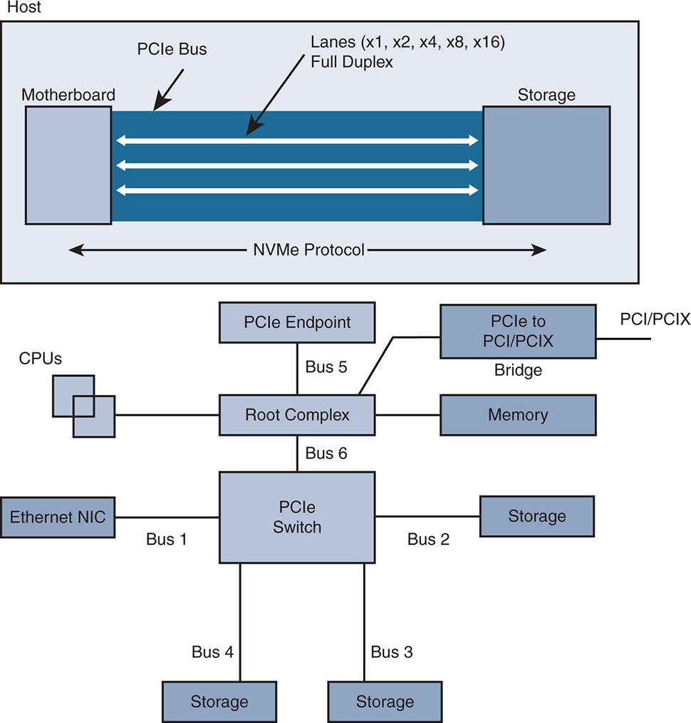
PCIe is a high-speed serial computer bus standard that offers a high-speed interconnect between the server motherboard and other peripherals such as Ethernet or storage devices. PCIe supersedes older parallel bus interconnect technologies such as PCI or PCI eXtended (PCIX). It is based on a point-to-point interconnect that consists of connecting multiple endpoints directly to a root complex. PCIe is based on lanes, each having two pairs of wires—one pair for transmit and another for receive—allowing full duplex “byte” communication. PCIe supports x1, x2, x4, x8, x16, and x32 lanes, with the biggest physical PCIe slot supporting currently 16 lanes. The “x,” as in “by,” indicates the total number of lanes. So “x4” indicates four lanes. Added lanes allow more bandwidth on the point-to-point connections. Figure 3-2 shows the point-to-point PCIe interconnects between endpoints. Note that two endpoints can have multiple lanes, offering added bandwidth.
Notice that the “root complex” allows connectivity to PCIe endpoints or a PCIe switch to provide connectivity to many more PCIe endpoints, such as storage devices or high-speed Ethernet network interface cards (NICs). Also, the root complex can connect to bridges for connectivity to legacy PCI/PCIX interfaces.
As data centers increase in scale and capacity, PCIe is needed to allow the adoption of higher capacity interconnects, such as the 100 GE NIC cards, or Infiniband (56 Gbps, 40 Gbps, 20 Gbps, 10 Gbps) and high-bandwidth I/O to storage peripherals.
The PCIe standard has gone through many revisions. The revisions that have enhanced the bandwidth are as follows:
- PCIe 1.a at 250 MBps data transfer rates per lane, or a transfer rate of 2.5 gigatransfers per second (GTps). The gigatransfer, or megatransfer, terminology refers to the raw data rate that the bus can move. The actual data rate is less because of the 8b/10b encoding where you need to send 10 bits of raw data for every 8 bits of actual data.
- PCIe 2.0 doubled the data transfer rate to 500 MBps or 5 GTps.
- PCIe 3.0 offers 1 GBps or 8 GTps.
- PCIe 4.0 doubled the data transfer to 2 GBps or 16 GTps.
- PCIe 5.0 at 4 GBps or 32 GTps per lane. This means that a 32-lane PCIe 5.0 interconnect can reach a full duplex data rate of 32 × 4 = 128 GBps.
Non-Volatile Memory Express
Non-Volatile Memory Express (NVMe) is a high-performance storage “protocol” that supports the PCIe technology. It was developed by the manufacturers of SSD drives to overcome the limitation of older protocols used with SATA drives, such as the Advanced Host Controller Interface (AHCI). AHCI is a hardware mechanism that allows the software to talk to SATA devices. It specifies how to transfer data between system memory and the device, such as a host bus adapter. AHCI offers, among other things, native command queuing (NCQ), which optimizes how read/write commands are executed to reduce the head movement of an HDD. Although AHCI was good for HDDs, it was not adequate for SSDs and PCIe interconnects.
It is important to note that NVMe is not an interface but rather a “specification” for the PCIe interface, and it replaces the AHCI protocol. NVMe is a protocol for accessing non-volatile memory, such as SSDs connected with PCIe buses. NVMe standardizes the register set, feature set, and command set for non-volatile memory. NVMe offers many attributes, such as these:
- High performance
- Low latency
- Better efficiency
- Lower CPU utilization
- Lower power
NVMe has driver support to a variety of operating systems, such as Windows Server, Free BSD, Ubuntu, Red Hat, and VMware. NVMe supports deep queues, such as 64,000 queues, where each queue supports 64,000 commands. This is in contrast to AHCI’s one command queue, which supports a total of 32 commands. Other specifications, such as better register access, interrupt handling, shorter command set, and others make NVMe a superior protocol for SSDs. Therefore, SSDs have the option of being connected via SAS or SATA interfaces, via PCIe, and via PCIe with an NVMe specification. With the NVMe interface, you now can take full advantage of the PCIe bus reaching performance of 128 GBps and beyond. Moving forward, specifications for NVMe over fabrics (NVMe-oF) transport the NVMe protocol over Ethernet to allow SSDs to be removed from inside the hosts and concentrated as centralized storage over an Ethernet network. Coupling NVMe-oF with Remote Direct Memory Access (RDMA) technology over Converged Ethernet (RoCE), which allows NIC cards to bypass the CPU in processing memory requests, allows much lower latencies in accessing SSD drives.
The combination of high-performance multicore processors, SSDs, PCIe, and advancement in NVMe paves the way for enormous bandwidth and performance in accessing storage devices.
Emergence of Flash-Based Products
In the same way that CPU and interconnects have evolved, storage hardware has continued to evolve with the enhancement in caching technology and the way storage arrays leverage cache for performance and slower HDD drives for capacity. Enhancement in flash technology paves the way for higher performance. However, early storage array products could not take full advantage of flash SSD because their products were designed for slower HDDs and slower bus interconnects.
Enhancement in Flash Technology
Flash memory has evolved dramatically over the years, and it is used in SSDs that are slowly replacing HDDs with spinning disks. Flash memory itself comes in several flavors, and there is a cost versus performance decision to be made in choosing the right flavor. Flash memory based on single-level cells (SLC) NAND (as in a NOT-AND gate) is very expensive, has high endurance, is reliable, and is used in high-performance storage arrays. Multilevel cell (MLC) NAND flash is less expensive, has lower endurance, is less reliable and has lower write performance. Traditional flash is called Planar NAND and is built on a single layer of memory cells. This introduced challenges in creating higher densities to lower the cost. A new type of flash called 3D is being introduced to produce higher densities by building multiple layers of memory cells. A new type of memory called 3D Xpoint was introduced to the market in 2017 by Intel and Micron, which promises to bridge the gap between NAND flash and RAM when considering speed versus cost per gigabyte.
All NAND flash memory suffers from what is called flash wear, in which the cells tend to deteriorate as writes are performed more frequently. Software needs to be aware of destroyed cells. The more cells are destroyed, the lower are the performances. An endurance measure for flash SSDs is in Total Bytes Written (TBW), which specifies the total terabytes that can be written per day on an SSD, during its warranty period, before the SSD starts failing. SLC flash with high TBW is normally used for caching, whereas MLC flash with lower TBW is used for lower cost flash capacity devices. Because every vendor’s objective is to extend the life of flash devices, mechanisms are adopted, such as wear-leveling, to spread the data across many blocks to avoid repetitive writing to the same block resulting in cell failure.
New Breed of Storage Arrays Falls Short
Chapter 2 discussed storage tiering and caching as enhancements to the traditional SAN arrays. The fact that storage arrays were becoming a bottleneck as many servers and virtual machines were accessing them prompted the emergence of new architecture. One such architecture is a redesign of storage arrays to handle all-flash SSDs or hybrid arrays with cache and HDD. It is worth discussing the new types of storage arrays because they will compete with hyperconvergence for market share.
All-Flash Arrays
Flash is now a strong contender for storage arrays because it offers many benefits, not only in speed and performance but in savings in power and cooling. A new breed of flash arrays started emerging, competing with HDD-based storage arrays on input/output operations per second (IOPS) and footprint. SSDs are used for capacity, and racks of HDD storage are now easily replaced with 2U or 4U chassis of SSDs, thereby saving on power consumption, cooling, and footprint.
Early products of flash arrays produced by the existing storage vendors were actually a variation of the same old storage array architectures. HDDs were changed to SSDs, which gave footprint savings; however, these systems were not designed for flash.
For instance, older storage arrays designed for HDDs used caching to handle both reads and writes in the storage controller to enhance the I/O performance while data is being written and read from spinning disk. These same architectures were adopted for all-flash arrays, where both reads and writes were handled in the cache, and not making use of the fast reads of SSDs. Also, write-in-place file systems were used, writing the same flash cells many times and causing flash wear. So, while early all-flash arrays had some performance improvements, they did not take full advantage of the expensive SSDs they used.
Other attributes that all-flash storage most overcome were the older architectures with SATA and SAS bus interconnects. Although SSDs offer a large number of IOPS, the bus interconnects were becoming the bottleneck. So, in summary, legacy storage vendors tried to jump on the all-flash bandwagon too fast and failed to deliver.
A new breed of flash arrays had to consider the characteristics of flash and high-speed interconnects to design systems from the ground up for better performance. While such newly designed systems are currently available on the market, they are still very expensive and cannot keep up with the huge growth in I/O processing in the data center. Although the flash drives gave much higher performance, the “centralized” dual storage controller architecture remains a bottleneck.
Hybrid Arrays
Hybrid refers to storage arrays that provide different tiers of storage with a combination of flash SSDs for cache and HDD disks for capacity. This, of course, generates a lot of confusion because any vendor who mixes HDD and SSD in their product can claim hybrid, including legacy products that support storage tiering. However, a savvy information technology (IT) professional needs to distinguish between older architectures designed for HDD and newer architectures designed for a combination of flash and HDDs. Many of the differentiations that were discussed in all-flash arrays apply here. Here are some things to look for:
- Is the storage array adopting the latest, faster, and denser HDDs, such as SAS?
- Can the storage array support PCIe and NVMe for flash cache drives?
- How does the controller deal with reads and writes?
- What is the power consumption of the system? Is it in the 1000 W range or the 10,000 W range?
- Where is compression and deduplication done: inline or post process?
- How does functionality such as compression and deduplication affect the performance of the application?
- Is the system doing storage tiering or storage caching?
Some or all of the above give an IT professional a clear idea of whether he is dealing with an older SAN storage array adapted to support flash, it is a new design that supports flash and has been adapted to support HDDs, or it is a system designed from day one to give the best performance to both.
Host-Based Caching
While all-flash storage arrays were evolving, a different architecture that focuses on the host side was evolving in parallel. Host-based caching moves some of the cache into the host for better performance than accessing the cache across the network. Instead of reaching across a SAN fibre channel or Ethernet network to access the storage array, caches were used on the host itself, which gives lower latency. This fast cache was used as the fast tier to do the read operations while the write operations were still done on traditional storage arrays. The drawback of this architecture is that some sort of tuning on the host caching software is needed on a per-application or a virtual machine basis. This adds a lot of overhead versus having all storage operations being taken care of by the storage array. Also, depending on the caching implementation, other drawbacks of the host-based caching architecture occur. In the case of a write-back cache, as an example, data is written to cache and acknowledged and then is sent in the background to the storage array. This results in data being trapped in the cache that does not participate with data management, such as taking snapshots from the storage array. As such, you are not getting consistent data management capabilities between the host cache and the storage array on the back end.
As the number of hosts increases, so does the cost of installing expensive cache cards inside the hosts, to the point where the costs become more than installing a centralized cache array. Although host-based caching is on the right path to hyperconvergence, by itself, it stands short of a complete solution. Evolution in storage software and the adoption of fully distributed storage file systems need to take place to achieve hyperconvergence.
Looking Ahead
This chapter covered the evolution in host hardware from compute to storage. This forms the basis of hyperconverged products that will use faster CPUs, high-speed interconnects, and high-performance flash drives.
Chapter 4, “Server Virtualization,” discusses the software evolution in the data center, starting from the advantages of virtualization in providing applications with high availability and reducing the footprint in data centers. Chapter 5, “Software-Defined Storage,” discusses the advantages of storage-defined networking in helping the industry move away from closed hardware-based storage arrays to a software-based architecture.