Chapter 12
Laser Printing of Electronic Materials
Philippe Delaporte1, Anne-Patricia Alloncle1 and Thomas Lippert2,3
1Aix-Marseille University, CNRS, LP3 Laboratory, 163 Avenue de Luminy, 13288 Marseille Cedex 9, France
2Paul Scherrer Institute, Neutrons and Muons Research Division, Thin Films and Interfaces Group, 5232 Villigen PSI, Switzerland
3ETH Zürich, Laboratory of Inorganic Chemistry, Department of Chemistry and Applied Biosciences, Vladimir-Prelog-Weg 1-5/10, 8093 Zürich, Switzerland
12.1 Introduction and Context
The development of printed electronics for industrial applications requires reliable and efficient digital printing techniques. For most of the applications, the challenge is no longer one of pitch size reduction, and the most relevant keywords are “flexible,” “low cost,” and “large area.” In this context, the typical dimension of the elementary unit is of the order of a few microns (3–50 µm), and the integration of many functions on the same device via one unique process is of paramount importance. Moreover, organic compounds present very interesting performance characteristics and are becoming increasingly suitable for device production. Two immediate candidates are the organic light-emitting diode (OLED), which will be used for the next generation of displays and for smart lighting applications, and the organic thin-film transistor (OTFT), which also becomes very attractive for a wide range of applications.
Two approaches are developed to manufacture these printed electronic devices: first, mass printing technologies (gravure printing, flexography, screen printing, etc.), which are well known from the graphic arts industry and enable roll-to-roll or high-speed sheet-to-sheet processing but require the use of an impression cylinder, which is designed for only one application. Second, noncontact and digital printing methods, especially inkjet printing, which has become widespread in the graphics industry, are seeing significant use for organic and printed electronics. All these conventional techniques require the use of liquid inks, and the quality of the deposition is critically dependant on the ink properties, notably viscosity, adhesion and separation properties, and drying, which all have a strong influence on the stability, shape, and lateral resolution of the deposit. The realization of multilayer structures is also complex with such processes because of the solvent compatibility between two successive layers. Indeed, the solvent used during the top layer deposition should not damage the bottom layer. The development of a simple process allowing the deposition of a wide variety of materials, with high spatial resolution (a few micrometers) is therefore of great interest for the manufacturing of future electronic devices.
As described in the previous chapters, laser-induced forward transfer (LIFT) allows printing a wide range of materials, organic or inorganic, in liquid or solid phase. LIFT is a single-step process, and dimensions of the printed pixels range typically from few micrometers to few millimeters, even if some submicrometer dots have already been LIFT-printed as described in Chapter 11. Moreover, this technique offers the possibility of transferring multilayer structures in a single step. Overall, LIFT appears as a very promising technology to overcome the challenges of printed electronic manufacturing.
Since the first experiment of LIFT performed by Bohandy et al. [1], for the deposition of copper film on a fused-silica substrate in vacuum using an ArF excimer laser (193 nm), many studies related to electronics applications have been reported. It is worth mentioning the use of LITI (see Chapter 1) for the fabrication of a functioning, large-area matrix backplane display circuits [2]. In 2004, Piqué et al. realized micropower sources [3] using a transfer process combining the advantages of LIFT and MAPLE (see Chapter 2). From 2007, the laser-induced forward transfer of organic materials led to the fabrication of functional organic electronic devices, such as polymer light-emitting diode (PLED) [4] and OTFT [5].
In this chapter, the pros and cons of LIFT as a manufacturing tool for printed electronics are discussed. First, the results of the studies dedicated to the fabrication of OTFT and OLED are presented. The main challenge relies on the ability of LIFT in transferring thin organic films without degrading their structural and electrical properties. The realization of passive components, such as capacitors, is also discussed. The last part is dedicated to the applications of LIFT for interconnection purposes, especially by transferring silver nanoparticle inks.
12.2 Organic Thin-Film Transistor
12.2.1 Operation and Characteristics of OTFTs
A growing interest in OTFTs has emerged due to their potential applications in electronics where low-cost, large-area coverage, and structural flexibility are required. The performance of OTFTs is often benchmarked against that of amorphous silicon (a-Si) TFTs with field-effect mobilities higher than μ = 1 cm2/Vs and on/off current ratios of Ion/off = 106–108. However, there is currently more emphasis on developing soluble materials that allow the combination of high mobility with good stability under air, moisture, and light exposure [6]. Solubility in organic solvents has become a critical parameter with regard to the implementation of organic semiconductors in the solution deposition technologies developed for printable electronics. Indeed, new organic semiconductor materials are developed and allow the fabrication of TFTs with remarkably high performance and exceptional durability and operational stability. However, these compounds do not possess the solubility features required for their application in printable electronics. LIFT appears as a unique solution to achieve digital printing of these compounds in solid phase and for the fabrication of high-performance OTFTs.
Figure 12.1 shows the different layered structures of an OFET comprising a gate electrode, a dielectric layer, source/drain (S/D) electrodes, and a semiconductor (SC) film. Depending on the sign of the gate bias, charge carriers can accumulate or be depleted at the semiconducting layer near the dielectric interface. The accumulated charge carriers pass from the source to the drain electrode upon application of a potential deference across the electrodes. The main challenges of OFET processing are to transfer each layer by consecutive printing processes without modifying their structural and electrical properties. Most of the studies performed on LIFT printing of OTFTs address the bottom gate configurations.

Figure 12.1 Schematic representation of the four configurations of a thin-film transistor structure.
Three parameters are considered to characterize the performances of thin-film transistors:
- The mobility (μ), which represents the ability of the carriers to move in the active layer (semiconductor) when a voltage (VD) is applied between the source and the drain electrodes. This physical parameter controls the current intensity at the drain electrode (ID) and the commutation time (tc), which defines the maximum operating frequency of the circuit. A higher mobility results in shorter commutation time, according to
12.1

where L is the channel length or the gap between the source and drain electrodes. The value of the mobility depends of the structural properties of the semiconductor material, and this parameter is also sensitive to the modifications induced by the printing process in this layer.
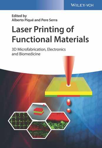
- The threshold voltage (VT) is defined by the following equation:
12.2
where d is the thickness of the semiconductor layer, Ci is the capacitance of the dielectric layer, q is the elementary charge, n0 is the carrier density, and Vfb is the voltage from the charge at the interfaces of the dielectric layer. For OTFTs, the threshold voltage must be as close as possible to zero. However, some parameters can contribute to modify this value, and among them, we must consider the presence of defects in the semiconductor layer as they can be induced during the printing process by the laser irradiation of this layer.
- The on/off current ratio (Ion/Ioff) is the ratio of the currents measured when the gate voltage (VG) switches from the Off state to the On state. The IOFF current, corresponding to VG = 0, should be, in theory, equal to zero as it characterizes the ability of the semiconductor layer to prevent the carrier flow between the source/drain electrodes when no seed carriers are injected. However, that is never the case for thin-film transistor because of the very small thickness of the layers and of the defects in the SC layer and at the interface with the dielectric layer. As these defects can be induced by the laser irradiation, this Ion/off parameter is also important to characterize the printing process.
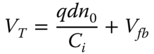
Two kinds of measurements are used to determine these parameters. First, the evolution of the drain current ID as a function of the drain voltage VD for different values of the gate voltage VG provides a first characterization of the OTFT operation. As shown in Figure 12.2a, there is first a linear dependence of the current versus the voltage and a saturation regime for the highest voltages. The second measurement is the evolution of the drain current as a function of VG for a given VD. A larger slope of the curve (see Figure 12.2b) results in a higher gain of the transistor. The field effect mobility μ is extracted from the transfer characteristics in the saturation regime. The drain–source current (ID) in the saturation regime is governed by the following equation:
where W is the channel width.
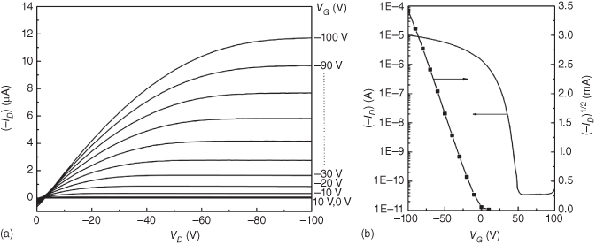
Figure 12.2 Typical output (a) and transfer (b) characteristics of a top contact OTFT.
Then, because charge carriers pass through the semiconducting layer near the dielectric layer, the semiconductor–dielectric interface characteristics and the structural properties of the semiconductor (crystallinity, defects, etc.) play a crucial role in the achievement of high-performance OTFTs. The characteristics of the dielectric layer are also important as the layer must be free of defects and have a uniform thickness to prevent leakage current. Another main parameter for the OTFT performance is the current injection through the source/drain electrodes. The work function of the source/drain electrodes must match the organic semiconductor electrical properties. A small change in the work function of the source/drain, potentially induced by surface degradation, will modify the contact resistance and can dramatically reduce the current. The properties of these thin films and their interfaces can be modified by the laser printing process, and the measurements of the three parameters (μ, VT, Ion/off) are used to determine the impact of the laser-induced transfer on the material properties and the OTFT performance.
The most challenging part of the printing process is the transfer of thin organic films. As demonstrated by Kim et al., the realization of the conductive layers (source/drain electrodes and gate) by laser printing of silver nanoparticle (Ag-NP) inks does not degrade the OTFT performances, compared to other deposition processes. They fabricated bottom-gate OTFTs in top- and bottom-contact configurations. The SC (Pentacene) and dielectric (PVP) layers were deposited by spin coating, and they LIFT-printed Ag-NP ink to form the electrodes. They obtained field-effect mobilities of approximately 0.16 cm2/V/s and on/off current ratios of approximately 105 [7]. The following paragraphs are dedicated to the influence of laser printing on the organic layer properties.
12.2.2 Laser Printing of the Semiconductor Layer
The following examples presented the realization and characterization of OTFTs in which the deposition of nonsoluble semiconductor material is achieved by LIFT in solid phase.
The first realization of LIFT-printed functional OTFTs, including the transfer of SC layer and S/D electrodes, was performed by Rapp et al. [5]. The semiconductor layer was a 100 nm thin film of copper phthalocyanine (CuPc), and the source/drain electrodes were printed from a silver nanoparticle ink. The OTFTs have been realized in top-contact (TC) and bottom-contact (BC) on a doped silicon substrate, which plays the role of the gate, covered by a 300 nm thin silicon dioxide (SiO2) film, which acts as the dielectric (Ci = 12 nF/cm2). Figure 12.3a shows an optical microscope image of this LIFT-printed structure. The electrical performances of these first LIFT-printed OTFTs were quite poor. For both BC and TC configurations, the mobilities were of few 10−5 cm2/V/s, and the On/Off current ratio was few 10−2. However, the performances of CuPc-based OTFTs realized by thermal evaporation under vacuum through a mask are only one order of magnitude better. These differences were probably due to the direct irradiation of CuPc film by the 355 nm picosecond laser that induced defects in the SC layer, and those defects can trap some of the carriers and reduce the mobility values.
Figure 12.3 Optical microscope image of a LIFT-printed OTFT. The substrate is a doped silicon wafer (gate) covered by a thin SiO2 layer (dielectric) on which are printed (a) CuPc SC pixels (blue–green) and Ag-NP ink lines (white) as S/D electrodes or (b) diPhAc-3T pixels, printed by LIFT, and gold electrodes evaporated with L = 80 µm.
Small-molecule semiconductor films have also been used for laser-printed OTFTs. Especially, the p-type organic semiconductor distyryl-quaterthiophene (DS4T) was vacuum-deposited on a donor substrate and transferred with picosecond laser pulses on Si/SiO2-based receiver substrates to form an organic active layer [8]. DS4T-based OTFTs realized by thermal evaporation showed a high field-effect mobility (0.02–0.04 cm2/V/s) but were also found to be exceptionally long-lived and stable toward continuous operation, under atmospheric conditions. As the DS4T films are very fragile, the direct irradiation of these films with a picosecond UV laser led to strong damages of the material. The transfer of such small-molecule compounds requires the use of a dynamic release layer (DRL – see Chapter 3) that absorbs the laser energy, transforms it in mechanical energy that propels the film forward, and prevents direct interaction of the laser light with the SC film. OTFT devices were realized in TC and BC configurations with gold evaporated S/D electrodes. The measured mobilities were similar to those obtained with the evaporated DS4T, but the ION/IOFF ratio was still low (few 103). These results show that the use of a DRL prevents the generation of light-induced defects in the semiconductor layer as the mobility is not degraded by the process. However, the strong mechanical effects due to the fast transfer (up to 500 m/s) of the pixel between the donor and the receiver lead to some modifications of the structure of the SC layer, which are probably responsible for the low current ratio. It is worth mentioning that these OTFTs exhibit very stable performances over time when stored in ambient conditions [8].
The diPhAc-3T (bis(2-phenylethynyl) end-substituted terthiophene) [9] compound has also been tested as organic semiconductor for the realization of thin-film transistors by means of laser printing. The specificity of this material is that the film growth is based on the island Volmer–Weber mechanism, which gives a structural cohesion to the film and makes it less sensitive to the mechanical damages potentially induced by laser irradiation. Indeed, atomic force microscopy analysis confirmed that the laser transfer did not modify the material structure, even when a DRL is not used [10]. TC diPhAc-3T-based OTFTs were fabricated on Si/SiO2 substrates with gold evaporated S/D electrodes (see Figure 12.3b). They exhibited good electrical performances (μ = 0.04 cm2/V/s, VT = 0 V, ION/IOFF = 2.8 × 10⁵), and the stability tests over 100 days were also very good [10]. These performances are similar to those obtained by thermal evaporation [9], which means that the laser printing process does not degrade the properties of the diPhAc-3T material.
In addition to these results obtained with nonsoluble SC compounds that suggest the great potential of LIFT for this application, other studies have been performed with soluble SC material, and the LIFT-printed OTFT performances were compared with those of inkjet-printed transistors. Among them, we would like to mention the poly-3-hexylthiophene (P3HT) semiconductor material[11, 12]. This semiconductor was printed on gold S/D electrodes sputtered on Si/SiO2 substrates. The morphological properties of the SC pixel were improved when using a titanium DRL; however, to avoid any risk of contamination by the DRL, the OTFTs were realized without DRL but using a thicker P3HT layer (150 nm). High mobility values were obtained, comparable with, or even higher than, those of inkjet-printed OTFTs, but with a low current ratio and high threshold voltage. This is probably due to some damages created in the very thin SiO2 layer (80 nm) by the impact of the transferred pixel or to some oxygen contamination at the SC–dielectric interface.
These different studies show that LIFT can be used to deposit SC pixels in solid phase for OTFT manufacturing. The irradiation parameters must be tuned to preserve the structural and electrical properties of the films. The use of a polymer DRL allows to prevent the direct irradiation of the film and therefore the generation of light- and thermally induced defects in the SC material. Another drawback of the laser printing process is the strong stress generated during the ejection from the donor and the landing on the receiver. This effect can modify the structural organization of the printed material and reduce the electrical performances of the OTFT devices. Then, organic semiconductors with high structural cohesion are the preferred choice if they are to be transferred by direct laser printing. For the tested materials, the mobilities of OTFTs with a laser-printed semiconductor were similar to those of OTFTs realized with a SC layer deposited by thermal evaporation.
12.2.3 Laser Printing of Dielectric Layers
Very few studies have been dedicated to laser printing of thin dielectric layers for the realization of OTFTs. The deposition of this layer is critical because both the interface with the semiconductor layer must be free of defects that could trap the carriers and its structure must be undamaged to avoid leakage currents. Diallo et al. performed an interesting experiment to investigate the effects of laser-printed dielectric layers on OTFT performances [13]. Figure 12.4 shows the three different OTFT configurations that have been realized and characterized. The substrate was a silicon (Si) wafer oxidized to form a 300 nm thick layer of SiO2 that is used as gate and dielectric in the first configuration (BG-OTFT1), which is completed by a 100 nm thick CuPc p-type semiconductor, thermally evaporated under high vacuum (HV), and finally, a 50 nm gold S/D electrode also thermally evaporated. The second configuration (BG-OTFT2) is almost identical, but a 600 nm PMMA layer is spin-coated on the SiO2 surface, which changes the dielectric capacitance from 12 to 5 nF/cm2 and the nature of the dielectric/SC interface. The last configuration (TG-OTFT3) is a top-gate design that is made from BG-OTFT1 by laser printing a PMMA layer and covering it with thermally evaporated aluminum. Then, the Si/SiO2 structure acts only as a substrate and the dielectric/SC interface is PMMA/CuPc as for BG-OTFT2.
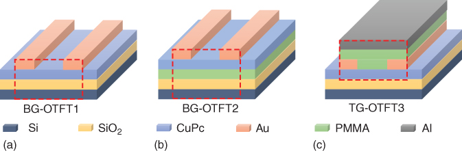
Figure 12.4 Schematic representation of the three OTFT configurations used to investigate the effects of laser printing of the dielectric layer on the OFTF characteristics. (a) BG-OTFT1: Si (gate)/SiO2 (dielectric)/CuPc (SC)/Au (S/D); (b) BG-OTFT2: Si (gate)/SiO2 + PMMA (dielectric)/CuPc (SC)/Au (S/D); (c) TG-OTFT3 CuPc (SC)/Au (S/D)/PMMA (dielectric)/Al (gate).
Table 12.1 presents the main characteristics of the thin-film transistors in the three configurations.
Table 12.1 Main characteristics of the thin-film transistors in the three configurations
| OTFT reference | μ (cm2/V s) | IOn/IOff | VT (V) |
| BG-OTFT1 | (1.7–2) × 10−3 | 8 × 10²–8 × 10⁴ | (−1.8)–(+9) |
| BG-OTFT2 | (3.1–3.5) × 10−3 | (1.3–3.3) × 105 | (−11)–(−16) |
| TG-OTFT3 | (7.3–8.6) × 10−3 | (0.5–1) × 102 | (−1)–(+55) |
The first observation is that the mobility value is almost the same for the three configurations. It is even slightly higher for the LIFT-printed PMMA, but that is probably due to the top-gate configuration. That means there is no degradation of the CuPc properties induced by the laser deposition of the PMMA layer on top of it. However, a large dispersion of the values of the threshold voltage (VT), from −1 to +55 V is observed for TG-OTFT3, revealing that the density of trap states to be filled before the carrier transport becomes mobile is higher than that for the other two configurations. This higher density of trap states is directly related to the LIFT process. As PMMA is slightly absorbent at the laser wavelength, these modifications certainly occur not only at the interfaces but also within the bulk material and close to the interface with the CuPc layer. Additionally, the low current ratio measured for the top-gate configuration, due to a high off-state current (IOff), underlines the presence of charges in the conducting channel at VG = 0 V. During the laser-induced transfer of PMMA layers, mechanical effects lead to some modifications of the morphology at the interface between the dielectric and the organic semiconductor, which is the interface where the charge transport occurs in such TG transistors.
The laser-induced transfer of dielectric layers is a critical step for the fabrication of thin-film transistors. It requires the use of a DRL to reduce the risk of material modifications, and as for SC layer, dielectric films with high structural cohesion are more suitable to improve the current ratio (IOn/IOff) parameter.
12.2.4 Laser Printing of Conducting Layers
The main material used for laser printing gates or S/D electrodes is silver nanoparticle ink [3, 14] because the transfer is done in liquid phase, and then there are no risks of stress-induced damage of the previous layer (SC or dielectric). However, the ink needs to be heated for sintering the silver nanoparticles, and this step can limit the use of polymers or substrates sensitive to temperature. As with the dielectric layer, there are only few studies dedicated to the LIFT printing of organic conductors for OTFT applications [15, 16].
Rapp et al. reported the fabrication of fully polymeric OTFT devices based on PQT-12 poly(3,3‴didodecylquaterthiophene) as semiconductor and PEDOT:PSS (poly(3,4-ethylenedioxythiophene)/poly(styrenesulfonate)) as conductor [16]. Both layers were LIFT-printed in solid phase with a UV picosecond laser on Si/SiO2 substrate acting as gate and dielectric. First, the OTFTs were printed PQT-12 transferred by laser and gold evaporated S/D electrodes. Their electrical characteristics showed a mobility of up to 5.10−3 cm2/V/ s−1 with a threshold voltage VT of –9 V and an IOn/IOff ratio of 103. The second set of OTFTs was formed with laser-printed PEDOT S/D electrodes instead of the evaporated Au electrodes. Their electrical performances were slightly improved. Mobilities of up to 0.02 cm2/V/s were measured with a threshold voltage VT of –20 V and an IOn/IOff ratio of 104. The semiconductor layer was the same for the two configurations of the transistors, and the increased mobility measured when PEDOT is used is attributed to a better interfacial contact between the two different polymer layers. Adequate contact between the printed PQT-12 and PEDOT:PSS is of prime importance, as it is essential for carrier's injection, which is the initial step to obtain operational OTFTs.
This result demonstrates that laser printing allows the fabrication of OTFT with conductor and semiconductor polymer materials transferred in solid phase. This approach gets rid of the solvent compatibility issue and opens the way of using a large set of organic materials.
12.2.5 Single-Step Printing of Full OTFT Device
LIFT offers the possibility of transferring a multilayer structure in a single step, and this approach has been used to print a full OTFT structure (gate/dielectric/SC) on S/D electrodes deposited on a substrate [17]. As shown in Figure 12.5, the donor substrate was composed of a triazene DRL [18], a silver layer (gate), a Parylene-C layer (dielectric), and a diPhAc-3T (SC). The receiver substrate was a silicon wafer with thermally evaporated gold electrodes. Under the laser irradiation of the DRL, the multilayer film (gate/dielectric/SC) is transferred over the electrodes to form a top-gate BC OTFT. Its electrical performances were a mobility 2 × 10⁻⁴ cm2/V/s, a threshold voltage VT of –4 V, and an IOn/IOff ratio up to 4 × 10⁴. These values are in the same range than those of transistors with similar structures and materials but fabricated by sequential evaporation steps. This single-step printing of a multilayer structure process offers the possibility to prepare large area donor film in a dedicated environment in which the interfaces between the different layers are optimized. Most of these interfaces are preserved as they do not interact with the atmosphere, and the realization of the transistor itself requires only the single step of laser transfer. For the transfer of very thick structures, the process can be optimized by using a smart beam shaping by increasing the fluence at the edges of the beam profile and reducing it in the center of the beam [19, 20].

Figure 12.5 Schematic representation of the single-step LIFT process used in the fabrication of multilayer structure for OTFT applications.
In conclusion, the OTFTs realized by laser printing yielded good electrical performance characteristics, which are comparable to those of the OTFTs fabricated by other printing techniques. Moreover, this is the only digital process allowing the use of such large range of materials. However, there are also some drawbacks. This technique induces some mechanical stresses into the material and can significantly modify its structural organization, which means that LIFT is particularly well suited for printing organic materials with high structural cohesion. Finally, the ablation mechanism occurring in the donor film also leads to the generation of a small amount of debris that is also transferred on the receiver. Careful optimization of the process allows to significantly reduce these effects, but it is almost impossible to fully get rid of them, and the debris might not be acceptable for some applications in printed electronics.
12.3 Organic Light-Emitting Diode
OLEDs have become a promising candidate for lighting and display applications. High-efficiency OLEDs require a multilayer device architecture to provide exciton confinement and balanced charge transport, and conventional pixelated OLED displays are mainly evaporated in HV through shadow masks. However, vacuum thermal evaporation bears the drawbacks of low material utilization rates, poor scalability, high capital cost, and difficulties in patterning. Solution processing and digital printing provide a low-cost approach to fabricate OLEDs and address applications as flexible electronics or personalized devices. Both inkjet and laser printing technologies are investigated to develop a reliable digital printing process for OLED manufacturing. Especially, many studies have been dedicated to the LITI process for the fabrication of OLED displays. In 2003, Samsung SDI presented the first full-color active-matrix OLED display prototypes fabricated with a LITI process step [21]. Nevertheless, thermal transfer defects were observed during the LITI process of vacuum-coated OLED materials [22].
This application of laser transfer to OLED manufacturing faces the same challenges as OTFT fabrication. Indeed, conditions must be found to print thin organic layers without inducing significant modifications of their physical, chemical, and electrical properties. The first LIFT-printed OLED was reported in 2007 by Fardel et al. [4]. They fabricated PLED with poly[2-methoxy-5-(2-ethylhexyloxy)-1,4-phenylenevinylene] (MEH-PPV) as light-emitting polymer (LEP). The typical architecture of the devices used glass as substrate covered by an ITO layer on which the LEP (90 nm) and aluminum (70 nm) layers are deposited. A current flowing between the two electrodes (Al–ITO) leads to a broad light emission from the MEH-PPV around 600 nm. For the LIFT experiments, the receiver substrate was a glass substrate covered by the ITO layer and the donor substrate was composed of a quartz substrate covered by the multilayer stack triazene/Al/LEP. A triazene polymer was used as a sacrificial layer (DRL) to preserve the material to be transferred from thermal effects, such as melting of the aluminum layer or degradation of the LEP. Light-emitting organic layers are very sensitive to laser irradiation, and the positive impact of using a sacrificial layer on the OLED performances has been demonstrated for different configurations [23, 24] The functionality of operating devices was characterized by current–voltage and electroluminescence measurements, which prove that the integrity of the transferred materials has been fully preserved during the LIFT deposition process. This first experiment demonstrated that functional PLED pixels can be fabricated by the DRL-LIFT process, and a luminance of 6 cd/m2 was measured at 14 V.
Based on the same device architecture and laser printing configuration, other materials and procedures have been investigated to realize RGB (red–blue–green) PLED devices with optimized performances [25]. Polyfluorene-based (PFO) polymers were studied as the electroluminescent material, as that allows to generate the green and red emission by blending triplet emitters as dopants into the PFO matrix. Devices were based on the architecture glass/140 nm ITO/60 nm PEDOT:PSS/40 nm PVK/∼50 nm LEP/cathode. The LEP was either plain for blue emission, or PFO doped with 5 wt% Ir(Me-ppy)3 for green emission, or with 5 wt% btp2Ir(acac) for red emission. Then donor substrates consisted typically of fused-silica/190 nm TP/80 nm cathode/PFO (<10 wt% triplet emitter dye, ∼50 nm). The ITO-on-glass receiver substrates were all coated with 60 nm PEDOT:PSS and 40 nm PVK as a hole-transporting layer. Figure 12.6 shows the structure of both the receiver and donor substrates, and Figure 12.7 presents the procedure to transfer the multilayer film. For all of these experiments, an approximately 15 µm donor–receiver substrate gap was used with a reduced environmental pressure of 1 mbar. The control of the pressure value allows to get rid of the shock wave generated by the laser interaction process (compared to atmospheric pressure) and to limit the velocity of the pixel (compared to vacuum) [26, 27].
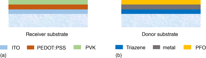
Figure 12.6 Structures of the receiver (a) and the donor (b) substrates.

Figure 12.7 A scheme of the red–green–blue PFO pixel transfer. The left image shows the transfer of the third, blue, pixel after the other two colors have already been transferred. The right image shows the receiver substrate alone with a bias across the three pixels creating electroluminescence.
Different cathode materials and irradiation conditions have been used to optimize the PLEDs' performances [28]: silver, aluminum, and aluminum with an ultrathin layer of the alkaline tetrabutylammonium hydroxide (TBA) directly deposited onto the electrode to help electron injection. Figure 12.8 shows microscopic images of the LIFT-printed RGB pixels with the Al and Al/TBA cathodes as well as the corresponding electroluminescent spectra.

Figure 12.8 Tricolor pixels imaged using a light microscope are shown for an Al/TBA cathode at 20 V (a) and for an Al cathode at 24 V (b). Electroluminescence (EL) spectra of tricolor LIFT pixels with an Al/TBA cathode (c) and with an Al cathode (d). On both graphs, the EL spectra of the “conventionally fabricated devices” are shown with a solid line and a color corresponding to the relevant device, and the printed pixels are represented with dotted lines and circles of corresponding color.
(Shaw-Stewart et al. 2012 [29]. Reproduced with permission of American Institute of Physics.)
Table 12.2 summarizes the performances of the PLED devices for different configurations. Luminance as high as 540 cd/m2 for the blue pixel and 232 and 145 cd/m2 have been obtained for the green and red pixel, respectively, after the optimization of the process, the materials, and the device configuration [29].
Table 12.2 Device performances for various device architectures, at a current density (CD) of approximately 40–50 mJ/cm2
| Color | Fabrication process | Bias (V) | CD (mJ/cm2) | Lum (cd/m2) | LE (CD/A) | EQE (%) |
| Blue | LIFT Al | 22 | 51 | 306.2 | 0.60 | 0.27 |
| LIFT Al/TBA | 21 | 48.32 | 540 | 0.89 | 0.40 | |
| Convent Al | 18 | 51.16 | 25.4 | 0.05 | 0.042 | |
| Convent Ca | 13 | 49.23 | 102.3 | 0.21 | 0.17 | |
| Green | LIFT Al | 26 | 37 | 134.5 | 0.36 | 0.11 |
| LIFT Al/TBA | 24 | 43 | 232.4 | 0.54 | 0.18 | |
| Convent Al | 39 | 48.9 | 715.6 | 1.46 | 0.46 | |
| Convent Ca | 22 | 44.5 | 3311 | 7.44 | 2.31 | |
| Red | LIFT Al | 19 | 35.67 | 84.7 | 0.24 | 0.15 |
| LIFT Al/TBA | 22 | 44.33 | 145.2 | 0.33 | 0.23 | |
| Convent Al | 40 | 47.9 | 14.5 | 0.03 | 0.043 | |
| Convent Ca | 18 | 45.14 | 726.5 | 1.64 | 2.32 |
Blue, green, and red refer to the LEP layer, whether just plain PFO (blue) or doped PFO (red and green). The “LIFT Al” are the LIFTed pixels with plain Al electrodes, “LIFT Al/TBA” are the LIFTed pixels with Al/tetrabutylammonium electrodes, the “Convent Al” are the conventionally fabricated devices with Al electrodes, and “Convent Ca” are the conventionally fabricated devices with Ca electrodes.
There is no doubt that laser printing is an appropriate process to realize PLED devices. Its ability to print multilayer films in a single-step process without reduction of the material performances is a great advantage over other printing technologies.
Sequential laser printing of the different layers has also been investigated for PLED fabrication and compared to single-step printing of multilayer films [30]. A 50 nm film of an alcohol-soluble polyfluorene (PFN) was transferred onto a receiver with a transparent anode, followed by the transfer of an aluminum cathode on top. Both printing steps were realized by the DRL-LIFT process under medium vacuum. The operation of the sequentially printed PLEDs requires higher voltages compared to the single-step printing PLEDs, and their efficiencies are slightly lower but still higher than those of the conventionally fabricated PLEDs with the same structure and materials. These differences are probably due to the higher roughness of the PFN surface induced by the LIFT process, and this surface corresponds to the interface with the aluminum cathode. However, this approach offers the advantage of transferring otherwise incompatible layers on top of one another and paves the way for the fabrication of more complex systems with improved device performances.
Small molecules have also been used to fabricate OLEDs by the LIFT process. This is more challenging than PLED printing because such small-molecule thin films have a much lower cohesion compared to polymeric films. A single-step transfer was used to deposit a multilayer film composed of TP-DRL/Al/TBA/Alq3 on a glass receiver covered by an ITO/PEDOT/PVK multilayer film. The LIFTed Alq3 pixels were functional, but their efficiencies were less than half the efficiencies of the conventionally fabricated Alq3 OLED devices. This is attributed to the mechanical load applied to the fragile Alq3 film during the transfer process [31]. This conclusion is consistent with the results previously discussed for OTFT fabrication where the laser printing process appears to have less of a negative influence for organic compounds with high structural cohesion.
Despite the interest of printing OLEDs in solid phase to avoid any solvent compatibility problems, laser printing has also been used to fabricate devices by transferring the compounds in liquid phase, similarly to the inkjet technique. Kattamis et al. [32] laser-printed different ionic transition metal complexes as the active layer on patterned ITO deposited on glass, and the fabrication of the OLED device is completed by vapor depositing an aluminum electrode through a shadow mask. They used the BA-LIFT (blister actuated LIFT) approach, described in Chapter 5, to transfer the electroluminescent material [33]. The devices exhibit performances in terms of electroluminescence emission, diode behavior, and lifetimes similar to those of spin-coated devices fabricated in nitrogen environments. The main advantage of this technique is its ability to work in an atmospheric environment by using air- and moisture-tolerant materials, and since the transfer in liquid phase is mechanically softer than LIFT in solid phase, there is no risk of mechanical damage of the structural properties of the printed materials. Moreover, as for DRL-LIFT, the polymer layer used to absorb and transfer the energy to the layer to be transferred blocks the direct interaction with the laser beam and thus prevents the light- or thermally induced degradation of the sensitive film. Finally, the use of thin donor film and a small laser spot size resulted in the printing of small OLED pixels with sizes down to 10 µm [33].
Quantum-dot-based light-emitting diodes also represent an attractive opportunity to produce LED displays because of the high color purity and photophysical stability of quantum dots [34]. Triazene DRL-LIFT was used to print semiconductor nanocrystal quantum dots. As previously presented, the active quantum-dot-based film was transferred together with an aluminum electrode onto a glass slide covered by an ITO transparent electrode. No degradation was observed in the luminescent efficiencies of the transferred NQDs. Indeed, the fluorescence spectra of the transferred NQDs were identical to those of the NQD layers deposited on the fused-silica donor substrate prior to the transfer process. Two different sizes of CdSe(CdS) nanoquantum dots, 5 and 6 nm, have been used, leading to photoluminescence in the yellow and red spectral range [35].
In conclusion, different techniques of laser printing (LITI, LIFT, DRL-LIFT, BA-LIFT) have been used to fabricate light-emitting diodes by transferring a large range of materials in liquid or solid phase. As for OTFT realization, the main risk of material damage when printing solid thin films is linked to the mechanical load induced by the fast ejection of the film. Organic compounds with high structural cohesion are preferable for laser-printed OLEDs. Very promising results were also obtained with quantum-dot-based active materials and organometallic electroluminescent materials.
12.4 Passive Components
Since the first demonstration of laser-induced forward transfer of copper in 1986 by Bohandy et al. [1], laser printing of conductive structures attracted lot of attention because of the large amount of potential applications, especially in microelectronics. MAPLE DW has been used to print various powders, including metals [36]. LIFT of solid metal thin films [37], silver nanoparticle inks [38], and silver pastes [39] has also been widely investigated to fabricate conductive structures.
The simplest electronic passive components, based on conductive materials, are resistors and inductors. Nickel–Chrome (NiCr) resistors were LIFT printed from NiCr donor films [36, 40]. Thicknesses up to 10 µm were obtained after 100 successive transfers. This parameter, as well as the planar geometry of the printed patterns and the material electrical properties, allows control of the resistance values. Laser printing resistors, with an accurate and easy-to-control value, can be considered as a postprocess to finely tune the operation of electronic circuits. When metal nanoparticle inks are used to print conductive patterns, the curing temperature of the deposited inks can also be used to control the resistive properties of the material [41]. Lasers are also used to achieve this sintering step, and an accurate selection of the irradiation parameters (wavelength, pulse duration, spatial distribution, fluence) provides a fine control of the resistivity value of the printed structures [42].
Capacitors have also been laser printed. In 2000, Chrisey et al. [40] transferred, by means of MAPLE DW, a 15 µm thick layer of BaTiO3 onto an evaporated gold electrode. The top gold electrode was printed by LIFT to form a capacitor of few pF at 1 MHz. Later, a single-step approach was used to transfer the top electrode with the dielectric onto a substrate covered with the bottom electrode, with a single laser shot. Poly-4-vinylphenol (PVP) and Shipley 1818 were used as dielectric with low viscosity, while silver ink and high-viscosity silver pastes were used as top electrode and Au as bottom electrode to obtain capacitors of a few tens of fF, and these values are in good agreement with the theoretical values [43]. With the same approach, capacitors were realized by transferring PVP, PMMA, or Parylene as dielectric with silver top electrodes on previously laser-printed silver bottom electrode [44–46]. For these experiments, a polymer DRL was used to protect the materiel to be transferred. Again, the measurements of the capacitance were in good agreement with the theoretical values. A morphological analysis of the printed structure shows that the strong pressure applied to the dielectric layer when reaching the electrode on the receiver induces a slight increase of its surface beyond the electrode area, which prevents any risk of short circuit between the two electrodes. This effect has also been observed when printing multilayer films for OLED fabrication [4]. The fabrication of microcapacitors from organic and inorganic materials, by using a single step, opens up the way for fast and cost-efficient fabrication of a large range of electrical devices, from conducting lines to complex components.
One of the challenges of the development of autonomous smart cards, which is one of the major markets of printed electronics, is the energy management. This requires energy harvesting systems (piezoelectric devices, solar cells, etc.) and printable microbatteries. In this context, laser processes have been used to fabricate Zn-Ag2O and Li-ion microbaterries [3]. Especially, the cathodes, Ag2O and LiMn2O4, were printed by the MAPLE DW technique, and laser scribing was used to isolate the cathodes from the anodes. Laser direct-write was also used to fabricate stacked Li-ion cells with 3.80 V open-circuit potentials [3]. They operated for more than 50 charge/discharge cycles without significant performance degradation. Capacitance values of 110 µAh/cm2 were obtained for batteries of 9.0 mm2 surface area. More recently, thick-film electrodes (LiCoO2 cathode and carbon anode) were laser-printed onto metallic current collectors for the fabricating Li-ion microbatteries. They exhibited a significantly higher discharge capacity and power density than those made by sputter-deposition thin-film techniques. This result has been attributed to the porous structure of the laser-printed electrodes that allows improved ionic and electronic transport through the thick electrodes (up to ∼100 µm) without a significant increase in internal resistance [47]. It has been proposed that the structuring effect of the printed LiCoO2 surfaces is due to a preferred orientation of the LiCoO2 particles that leads to a higher roughness when the number of layers increases [48].
12.5 Interconnection and Heterogeneous Integration
Printing conductive lines could appear as the simplest step of manufacturing printed electronic devices. However, the large number of applications requires a process that is able to print thin and thick lines (from 100 nm to 5 µm) with a minimum width of 10 µm and a width uniformity better than a few micrometers (±2 µm). Moreover, the process must be reliable and fast (>1 m/s). Inkjet is the most currently used digital process, but it suffers from drawbacks such as the high probability to get clogged nozzles and its limitation to transfer only low-viscosity inks, between 6 and 20 mPa s. Laser printing has been extensively investigated to address this topic. Two main approaches have been considered: first, the transfer of silver nanoparticle inks or pastes, and more recently, the printing of metal in liquid phase from a solid thin donor film.
The physics of printing lines by means of LIFT of liquids, such as inks, is presented in Chapter 4, and it will not be discussed here. The standard approach to deposit a continuous line is to print adjacent droplets with a controlled overlap. The value of this overlap must be high enough to guarantee the continuity of the line but not too high to avoid the formation of bulging. To avoid this bulging effect, one can use alternate printing of two overlapping sets of droplets with an intermediate drying step [49]. The morphological properties of the silver lines also depend on the surface energy of the receiver and the ink viscosity [38]. In order to increase the printing velocity, high-repetition-rate lasers, up to 1 MHz, were used to transfer microdroplets of silver inks [50]. It has been demonstrated, both experimentally [51] and numerically [52], that when two successive laser irradiations of the donor film are too close, in time and space, the cavitation bubbles generated in the liquid film interact and form tilted and instable jets. Based on this knowledge, continuous silver lines of 20 µm width have been printed with a three-pass approach at velocities up to 4 m/s [53]. In order to further increase the printing velocity, the distance between two consecutive laser spots can be decreased, leading to the formation of a large gas bubble and the transfer of a full continuous line instead of a set of liquid jets [54]. This approach allows printing silver lines in a single step at velocities up to 17 m/s without any risk of bulging. Figure 12.9 shows an illustration of this single-step transfer of a continuous line. After the transfer of the metal inks on the substrate, a sintering step is required to evaporate the solvent and sinter the particles in order to obtain conductive lines, and as mentioned previously, laser processes can be used to perform this step [41, 55, 56].
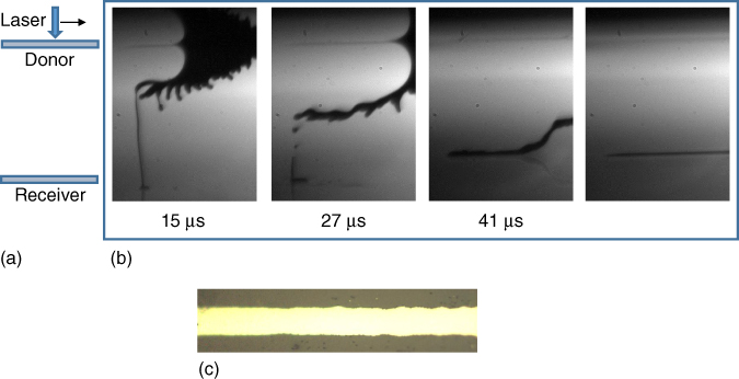
Figure 12.9 LIFT of a continuous line of silver inks in a single step at high velocity. The silver ink (Sun chemical U5714) has a viscosity of 11 mPa s and contains 40% of silver nanoparticle in weight. The UV picosecond laser operates at 1 MHz and scans the donor film at velocity of 17 m/s. (a) Schematic illustration of the setup. (b) Shadowgraphy images showing the formation of a large gas bubble in the donor film and the transfer dynamics of the continuous line toward the receiver substrate. (c) Optical microscopic image of the printed line showing a very uniform width of 25 µm.
These conductive lines are used to realize passive components as discussed previously, but also to connect the different devices of a printed circuit board. The integration of silicon-based circuits on smart cards or RFID cards requires the connection between the printed components (sensors, display, antenna, etc.) and the pads of the silicon chips. The width of these pads is typically around 50 µm, and the distance between two pads is of the order of 10 µm. To avoid any risk of short circuits, this step requires printing lines with small width (<40 µm) and with high resolution (better than 5 µm). To date, laser printing is the best candidate to realize this connection step at high velocity. Another important application of printing high-resolution conductive lines is the fabrication of interdigitized electrodes for sensors. Figure 12.10 shows two examples of such electrodes LIFT-printed at a velocity of 17 m/s on flexible PET substrates.

Figure 12.10 Interdigitized electrodes LIFT-printed from silver nanoparticle inks with a UV picosecond laser operating at 1MHz and a scanner system to move the laser over the donor substrate. (a) Line width of 25 µm and distance between lines of 100 µm, (b) line width of 100 µm and distance between lines of 80 µm.
The laser printing of silver nanopastes also offers a wide range of possibilities. Indeed, this high-viscosity material (105 mPa s) combines the advantages of solids (preserve the shape of the beam, printing of thick layers) and those of liquids (no debris) [57, 58]. The realization of thick and narrow conducting lines is of great interest for applications that require high current [59], especially photovoltaic manufacturing [60]. Thanks to the mechanical properties and the soft nature of the nanopastes, freestanding structures, such as bridges or cantilevers, have been laser-printed in a single step [61], and that opens the way for the realization of MEMS devices on printed electronics cards. Printing bridges is also a unique single-step method to interconnect pads over another connection line without using an insulating intermediate layer [62].
Flip-chip technology is used to connect the chip to the substrate via conductive bumps. Many bumping techniques are used, but they presented some drawbacks such as the high processing temperatures or the lack of flexibility. LIFT has been used to bond vertical-cavity surface-emitting lasers (VCSELs) to silicon grating couplers (GCs) [63] and single dies to gold contact pads deposited on glass [64]. For both experiments, indium metal pixels were LIFTed onto the receiver to form bumps of 20 µm diameter and few micrometers of thickness. Then, thermocompression bonding was used to ensure the final adhesion. The characteristics of the LIFT-bonded devices were similar to those assembled with other technologies, but the LIFT process is much simpler. In addition, LIFT enables the bumping and bonding down to chip scale, which is critical for fabricating ultraminiature circuitry. The realization of chip bonding on flexible substrate is even more challenging because of the mechanical stresses induced when the substrate is bent. Isotropic conductive adhesive (ICA) is often used to mount devices on conductive pastes deposited on plastic substrates. Sridhar et al. LIFT-printed ICA pixels and demonstrated the applicability of this process using RFID transponder integration and testing [65]. They performed the transfer experiment with and without polymer DRL, and no significant differences were observed. Some devices were realized with the LIFT process and others with the stencil printing technique. Their electrical and mechanical characteristics were compared, and the authors concluded that the LIFT process does not affect the electrical and reliability characteristics of the joints formed by the tested ICA. LIFT offers, therefore, a simple, highly accurate, and flexible solution to realize chip-level interconnections for applications requiring single-chip bumping, high-accuracy, and fine pitch for high-density flip-chip applications.
In 2006, Piqué et al. proposed and demonstrated a laser-based process to fabricate embedded circuits [66]. The heterogeneous integration consists in mixing silicon chips and printed elements to realize low-cost smart cards. This requires to connect, as previously discussed, and embed chips in plastic. The authors used first laser ablation to realize the cavities in a plastic substrate, followed by the LIFT of different electronic chips into these cavities. Then an insulating layer is spin-coated to encapsulate the chips and access to the connections that are realized by means of LIFT of conductive pastes is realized by laser drilling. This approach is easy to implement compared to standard microelectronic techniques and opens the door for the fabrication of embedded electronic circuits, which are the building blocks for the development of 3D Systems-in-Package (3D-SiP) microelectronics.
All these ink- or paste-based approaches, developed to print conductive structures, present many advantages compared to other digital printing technologies, such as inkjet, but they still require a sintering step to obtain good conductivity. For the past few years, some groups have combined thin metal donor films with short laser pulses and small focal spot to transfer the metal in liquid phase. Indeed, an appropriate choice of the laser fluence and pulse duration allows to deliver an amount of energy in the thin metal film slightly higher than the energy required to melt it but lower than the energy that would induce its total vaporization [67]. This approach, discussed in greater detail in Chapter 17, has been successively used to print high-aspect-ratio gold pillars of 3–5 µm diameter and 2.1 mm long [68] and nanodots of silicon [69] and gold [70]. The great benefit of this process is that it removes the sintering step because the droplets solidify when reaching the receiver substrate. Conducting lines of copper, aluminum, and gold have been printed with a high resolution and minimum width down to 2 µm [71, 72]. Studies have been performed to investigate the effect of oxidation of melted metal droplets during their transfer on the conductivity of the printed lines. They showed that the electrical transport mechanism in the laser-printed copper structures is different than that in aluminum structures. Copper structures have resistivity as low as approximately 4× of bulk copper, and oxidation does not significantly increase this resistivity [73] as it does in aluminum structures, for which resistivity values have been measured between 4.9× and 470× of the bulk material [74]. For printed aluminum, the increase in resistivity is due to the formation of an aluminum-oxide shell surrounding each droplet. Smaller droplets result therefore in a higher resistivity increase, and printing in inert gas atmosphere prevents the oxidation of the droplets and low resistivity structures can be printed. It is worth mentioning that the company Orbotec has developed a laser printing process based on this approach to repair the interconnection defects of printed circuit board.
12.6 Conclusion
Laser printing has a huge potential for electronic applications. Its ability to deposit small amounts of a wide range of materials with very high resolution makes it a unique tool for digital manufacturing of many electronic devices. The use of LIFT to transfer thin layers or multilayer stacks for the fabrication of OLEDs or OTFTs offers many possibilities but still has some drawbacks, for example, related to the generation of debris that can make the process irrelevant for ultraclean applications. Moreover, the generation of the shock wave induced by the transfer in solid phase requires the use of low gas pressure environment or/and a small gap between the receiver and the donor. When it is compatible with the application, a thin soft layer can be deposited on the receiver, and this lowers the impact and helps preserve the properties of the transferred material [75]. Despite these drawbacks, LIFT succeeds in printing OTFTs and OLEDs with performances similar or higher than those printed with conventional digital techniques.
The transfer of conductive structures, from metal inks or pastes or directly from solid thin films, is probably the most relevant application of this process for the microelectronics industry. Lines as narrow as 2 µm have been printed, and that is more than 10 times smaller than any other digital printing technology can achieve. All kinds of materials can be printed with very high resolution and at high velocities. The deposition of solid metals in liquid phase allows the printing of metal structures with low resistivity without the need for a sintering step. This process also offers the possibility to print very thick lines for high current flow and 3D structures such as bridges or MEMS and will be covered in more detail in Chapter 17.
Laser-based processes already addressed several manufacturing steps for electronics. In addition to drilling, scribing, cutting, and sintering, laser printing is becoming a mature process offering new opportunities for the development of electronic products [76]. Its ability to transfer a wide range of materials on various kinds of substrates and with high resolution makes it especially suitable for heterogeneous integration, which is considered a very relevant approach for the fabrication of low-cost electronic products, especially on flexible substrates. The digital and contact-free characteristics of the laser printing technology open new possibilities for the realization of personalized products or for adding new functions to standard products such as RFID tags. Furthermore, this technique is especially relevant to address the challenges of interconnection. That is a unique contact-free process for printing high-aspect-ratio conductive lines, narrower than 10 µm and thicker than few micrometers, to both increase the level of integration and enable the transmission of high currents, and for printing 3D structures for connecting the different levels of devices found in 3D-Systems-in-Package assemblies. As this chapter has shown, laser printing is poised to become a key technology for manufacturing the next generations of smart cards on plastic or flexible substrates.
References
- 1 Bohandy, J., Kim, B.F., and Adrian, F.J. (1986) Metal deposition from a supported metal film using an excimer laser. J. Appl. Phys., 60 (4), 1538–1539.
- 2 Blanchet, G.B., Loo, Y.-L., Rogers, J.A., Gao, F., and Fincher, C.R. (2003) Large area, high resolution, dry printing of conducting polymers for organic electronics. Appl. Phys. Lett., 82, 463.
- 3 Piqué, A., Arnold, C.B., Kim, H., Ollinger, M., and Sutto, T.E. (2004) Rapid prototyping of micropower sources by laser direct-write. Appl. Phys. A, 79, 783–786.
- 4 Fardel, R., Nagel, M., Nuesch, F., Lippert, T., and Wokaun, A. (2007) Fabrication of organic light-emitting diode pixels by laser-assisted forward transfer. Appl. Phys. Lett., 91, 061103.
- 5 Rapp, L., Diallo, A.K., Alloncle, A.-P., Videlot-Ackerman, C., Fages, F., and Delaporte, P. (2009) Pulsed-laser printing of organic thin film transistors. Appl. Phys. Lett., 95, 171109.
- 6 Kang, B., Lee, W.H., and Cho, K. (2013) Recent advances in organic transistor printing processes. ACS Appl. Mater. Interfaces, 5 (7), 2302–2315.
- 7 Kim, H., Auyeung, R.C.Y., Lee, S.H., Huston, A.L., and Piqué, A. (2009) Laser forward transfer of silver electrodes for organic thin-film transistors. Appl. Phys. A, 96, 441–445.
- 8 Rapp, L., Diallo, A.K., Nénon, S., Alloncle, A.-P., Videlot-Ackerman, C., Fages, F., Nagel, M., Lippert, T., and Delaporte, P. (2012) Laser printing of a semiconducting oligomer as active layer in organic thin film transistors: impact of a protecting triazene layer. Thin Solid Films, 520, 3043–3047.
- 9 Diallo, A.K., Videlot-Ackermann, C., Marsal, P., Brisset, H., Fages, F., Kumagai, A., Yoshimoto, N., Serein-Spirau, F., and Lere-Porte, J.P. (2010) Acetylenic spacers in phenylene end-substituted oligothiophene core for highly air-stable organic field-effect transistors. Phys. Chem. Chem. Phys., 12, 3845–3851.
- 10 Rapp, L., Serein-Spirau, F., Lère-Porte, J.-P., Alloncle, A.-P., Delaporte, P., Fages, F., and Videlot-Ackermann, C. (2012) Laser printing of air-stable high performing organic thin film transistors. Org. Electron., 13 (10), 2035–2041.
- 11 Zergioti, I., Makrygianni, M., Dimitrakis, P., Normand, P., and Chatzandroulis, S. (2011) Laser printing of polythiophene for organic electronics. Appl. Surf. Sci., 257, 5148–5151.
- 12 Makrygianni, M., Verrelli, E., Boukos, N., Chatzandroulis, S., Tsoukalas, D., and Zergioti, I. (2013) Laser printing and characterization of semiconducting polymers for organic electronics. Appl. Phys. A, 110, 559–563.
- 13 Diallo, A.K., Rapp, L., Nénon, S., Alloncle, A.P., Delaporte, P., Fages, F., and Videlot-Ackermann, C. (2011) Top gate copper phthalocyanine thin film transistors with laser-printed dielectric. Synth. Met., 161, 888–893.
- 14 Kim, H., Auyeung, R.C.Y., Lee, S.H., Huston, A.L., and Piqué, A. (2010) Laser-printed interdigitated Ag electrodes for organic thin film transistors. J. Phys. D: Appl. Phys., 43, 085101.
- 15 Thomas, B., Alloncle, A.-P., Delaporte, P., Sentis, M., Sanaur, S., Barret, M., and Collot, P. (2007) Experimental investigations of laser induced forward transfer process of organic thin films. Appl. Surf. Sci., 254 (4), 1206–1210.
- 16 Rapp, L., Constantinescu, C., Delaporte, P., and Alloncle, A.P. (2014) Laser-induced forward transfer of polythiophene-based derivatives for fully polymeric thin film transistors. Org. Electron., 15 (8), 1868–1875.
- 17 Constantinescu, C., Diallo, A.K., Rapp, L., Cremillieu, P., Mazurczyk, R., Serein-Spirau, F., Lere-Porte, J.P., Delaporte, P., Alloncle, A.P., and Videlot-Ackermann, C. (2015) Laser-induced forward transfer of multi-layered structures for OTFT applications. Appl. Surf. Sci., 336, 11–15.
- 18 Karnakis, D., Lippert, T., Ichinose, N., Kawanishi, S., and Fukumura, H. (1998) Laser induced molecular transfer using ablation of a triazeno-polymer. Appl. Surf. Sci., 127–129, 781.
- 19 Auyeung, R.C.Y., Kim, H., Mathews, S., and Piqué, A. (2015) Laser forward transfer using structured light. Opt. Express, 23 (1), 422–430.
- 20 Rapp, L., Constantinescu, C., Larmande, Y., Alloncle, A.P., and Delaporte, P. (2014) Smart beam shaping for the deposition of solid polymeric material by laser forward transfer. Appl. Phys. A, 117 (1), 333–339.
- 21 Lee, S.T., Suh, M.C., Kang, T.M., Kwon, Y.G., Lee, J.H., Kim, H.D., and Chung, H.K. (2007) 53.1: invited paper: LITI (laser induced thermal imaging) technology for high-resolution and large-sized AMOLED. SID Int. Symp. Digest Tech. Pap., 38, 1588–1591. doi: 10.1889/1.2785622.
- 22 Lamansky, S., Hoffend, T.R., Le, H., Jones, V., Wolk, M.B., and Tolbert, W.A. (2005) Laser induced thermal imaging of vacuum-coated OLED materials. SPIE Proc., 5937, 593702.
- 23 Kattamis, N.T., McDaniel, N.D., Bernhard, S., and Arnold, C.B. (2009) Laser direct write printing of sensitive and robust light emitting organic molecules. Appl. Phys. Lett., 94, 103306.
- 24 Ko, S.H., Pan, H., Lee, D., Grigoropoulos, C.P., and Park, H.K. (2010) Nanoparticle selective laser processing for a flexible display fabrication. Jpn. J. Appl. Phys., Part 1, 49, 05EC03.
- 25 Shaw-Stewart, J., Lippert, T., Nagel, M., Nuesch, F., and Wokaun, A. (2011) Laser-induced forward transfer of polymer light-emitting diode pixels with increased charge injection. ACS Appl. Mater. Interfaces, 3 (2), 309–316.
- 26 Fardel, R., Nagel, M., Nuesch, F., Lippert, T., and Wokaun, A. (2010) Laser-induced forward transfer of organic LED building blocks studied by time-resolved shadowgraphy. J. Phys. Chem. C, 114, 5617–5636.
- 27 Shaw-Stewart, J., Chu, B., Lippert, T., Maniglio, Y., Nagel, M., Nüesch, F., and Wokaun, A. (2011) Improved laser-induced forward transfer of organic semiconductor thin films by reducing the environmental pressure and controlling the substrate–substrate gap width. Appl. Phys. A, 105, 713–722.
- 28 Shaw-Stewart, J., Mattle, T., Lippert, T., Nagel, M., Nüesch, F., and Wokaun, A. (2013) The optimisation of the laser-induced forward transfer process for fabrication of polyfluorene-based organic light-emitting diode pixels. Appl. Surf. Sci., 278, 341–346.
- 29 Shaw-Stewart, J., Lippert, T., Nagel, M., Nüesch, F., and Wokaun, A. (2012) Red-green-blue polymer light-emitting diode pixels printed by optimized laser-induced forward transfer. Appl. Phys. Lett., 100, 203303.
- 30 Shaw-Stewart, J., Lippert, T., Nagel, M., Nüesch, F., and Wokaun, A. (2012) Sequential printing by laser-induced forward transfer to fabricate a polymer light-emitting diode pixel. Appl. Mater. Interfaces, 4, 3535–3541.
- 31 Shaw-Stewart, J., Mattle, T., Lippert, T., Nagel, M., Nuesch, F.A., and Wokaun, A. (2013) The fabrication of small molecule organic light-emitting diode pixels by laser-induced forward transfer. J. Appl. Phys., 113, 043104.
- 32 Kattamis, N.T., McDaniel, N.D., Bernhard, S., and Arnold, C.B. (2011) Ambient laser direct-write printing of a patterned organo-metallic electroluminescent device. Org. Electron., 12, 1152–1158.
- 33 Kattamis, N.T., Purnick, P.E., Weiss, R., and Arnold, C.B. (2007) Thick film laser induced forward transfer for deposition of thermally and mechanically sensitive materials. Appl. Phys. Lett., 91, 171120.
- 34 Lim, J., Bae, W.K., Kwak, J., Lee, S., Lee, C., and Char, K. (2012) Perspective on synthesis, device structures, and printing processes for quantum dot displays. Opt. Mater. Express, 2 (5), 594.
- 35 Xu, J., Liu, J., Cui, D., Gerhold, M., Wang, A.Y., Nagel, M., and Lippert, T. (2007) Laser-assisted forward transfer of multi-spectral nanocrystal quantum dot emitters. Nanotechnology, 18, 025403.
- 36 Piqué, A., Chrisey, D.B., Auyeung, R.C.Y., Fitz-Gerald, J., Wu, H.D., McGill, R.A., Lakeou, S., Wu, P.K., Nguyen, V., and Duignan, M. (1999) A novel laser transfer process for direct writing of electronic and sensor materials. Appl. Phys. A, 69, 279–284.
- 37 Zergioti, I., Mailis, S., Vainos, N.A., Papakonstantinou, P., Kalpouzos, C., Grigoropoulos, C.P., and Fotakis, C. (1998) Microdeposition of metal and oxide structures using ultrashort laser pulses. Appl. Phys. A, 66, 579–582.
- 38 Rapp, L., Ailuno, J., Alloncle, A.-P., and Delaporte, P. (2011) Pulsed-laser printing of silver nanoparticles ink: control of morphological properties. Opt. Express, 19 (22), 21563–21574.
- 39 Duocastella, M., Kim, H., Serra, P., and Piqué, A. (2012) Optimization of laser printing of nanoparticle suspensions for microelectronic applications. Appl. Phys. A, 106, 471–478.
- 40 Chrisey, D.B., Pique, A., Fitz-Gerald, J., Auyeung, R.C.Y., McGill, R.A., Wu, H.D., and Duignan, M. (2000) New approach to laser direct writing active and passive mesoscopic circuit elements. Appl. Surf. Sci., 154–155, 593–600.
- 41 Makrygianni, M., Kalpyris, I., Boutopoulos, C., and Zergioti, I. (2014) Laser induced forward transfer of Ag nanoparticles ink deposition and characterization. Appl. Surf. Sci., 297, 40–44.
- 42 Chung, J., Ko, S., Bieri, N.R., Grigoropoulos, C.P., and Poulikakos, D. (2004) Conductor microstructures by laser curing of printed gold nanoparticle ink. Appl. Phys. Lett., 84 (5), 801–803.
- 43 Birnbaum, A. J., Kim, H., Charipar, N. A., Piqué, A. (2010) Laser printing of multi-layered polymer/metal heterostructures for electronic and MEMS devices, Appl. Phys. A 99, 711–716.
- 44 Constantinescu, C., Rapp, L., Diallo, A.K., Videlot-Ackermann, C., Delaporte, P., and Alloncle, A.-P. (2015) Microcapacitors with controlled electrical capacity in the pF–nF range printed by laser-induced forward transfer (LIFT). Org. Electron., 20, 1–7.
- 45 Constantinescu, C., Rapp, L., Delaporte, P., and Alloncle, A.-P. (2016) Investigation on laser printing of microcapacitors using poly (methyl methacrylate) dielectric thin films for organic electronics applications'. Appl. Surf. Sci., 374, 90–95.
- 46 Constantinescu, C., Rapp, L., Rotaru, P., Delaporte, P., and Alloncle, A.-P. (2016) Polyvinylphenol (PVP) microcapacitors printed by laser-induced forward transfer (LIFT): multilayered pixel design and thermal analysis investigations. J. Phys. D: Appl. Phys., 49, 155301.
- 47 Kim, H., Proell, J., Kohler, R., Pfleging, W., and Piqué, A. (2012) Laser-printed and processed LiCoO2 CathodeThick films for Li-Ion microbatteries. J. Laser Micro/Nanoeng., 7 (3), 320–325.
- 48 Atre, A.C. and Arnold, C.B. (2011) LiCoO2 texturing by laser induced forward transfer for printed microbatteries. SPIE Proc., 7921, 79210O.
- 49 Florian, C., Caballero-Lucas, F., Fernández-Pradas, J.M., Artigas, R., Ogier, S., Karnakis, D., and Serra, P. (2015) Conductive silver ink printing through the laser-induced forward transfer technique. Appl. Surf. Sci., 336, 304–308.
- 50 Biver, E., Rapp, L., Alloncle, A.-P., and Delaporte, P. (2014) Multi-jets formation using laser forward transfer. Appl. Surf. Sci., 302, 153–158.
- 51 Biver, E., Rapp, L., Alloncle, A.-P., Serra, P., and Delaporte, P. (2014) High-speed multi-jets printing using laser forward transfer: time-resolved study of the ejection dynamics. Opt. Express, 22 (14), 17122–17134.
- 52 Brasz, C.F., Yang, J.H., and Arnold, C.B. (2015) Tilting of adjacent laser-induced liquid jets. Microfluid. Nanofluid., 18, 185–197.
- 53 Rapp, L., Biver, E., Alloncle, A.-P., and Delaporte, P. (2014) High-speed laser printing of silver nanoparticles ink. J. Laser Micro/Nanoeng., 9 (1), 5–9.
- 54 Puerto, D., Biver, E., Alloncle, A.-P., and Delaporte, P. (2016) Single step high-speed printing of continuous silver lines by laser-induced forward transfer. Appl. Surf. Sci., 374, 183–189.
- 55 Son, Y., Yeo, J., Moon, H., Lim, T.W., Hong, S., Nam, K.H., Yoo, S., Grigoropoulos, C.P., Yang, D.-Y., and Ko, S.H. (2011) Nanoscale electronics: digital fabrication by direct femtosecond laser processing of metal nanoparticles. Adv. Mater., 23, 3176–3181.
- 56 Joo, M., Lee, B., Jeong, S., and Lee, M. (2012) Comparative studies on thermal and laser sintering for highly conductive Cu films printable on plastic substrate. Thin Solid Films, 520, 2878–2883.
- 57 Auyeung, R.C.Y., Kim, H., Charipar, N.A., Birnbaum, A.J., Mathews, S.A., and Piqué, A. (2011) Laser forward transfer based on a spatial light modulator. Appl. Phys. A, 102, 21–26.
- 58 Piqué, A., Auyeung, R.C.Y., Kim, H., Metkus, K.M., and Matthews, S.A. (2008) Digital microfabrication by laser decal transfer. J. Laser Micro/Nanoeng., 3 (3), 163–169.
- 59 Breckenfeld, E., Kim, H., Auyeung, R.C.Y., Charipar, N., Serra, P., and Piqué, A. (2015) Laser-induced forward transfer of silver nanopaste for microwave interconnects. Appl. Surf. Sci., 331, 254–261.
- 60 Sanchez-Aniorte, M.I., Mouhamadou, B., Alloncle, A.-P., Sarnet, T., and Delaporte, P. (2016) Laser-induced forward transfer for improving fine-line metallization in photovoltaic applications. Appl. Phys. A, 122, 595.
- 61 Auyeung, R.C.Y., Kim, H., Birnbaum, A.J., Zalalutdinov, M., Mathews, S.A., and Piqué, A. (2009) Laser decal transfer of freestanding microcantilevers and microbridges. Appl. Phys. A, 97, 513–519.
- 62 Wang, J., Auyeung, R.C.Y., Kim, H., Charipar, N.A., and Piqué, A. (2010) Three-dimensional printing of interconnects by laser direct-write of silver nanopastes. Adv. Mater., 22, 4462–4466.
- 63 Kaur, K.S., Subramanian, A.Z., Cardile, P., Verplancke, R., Van Kerrebrouck, J., Spiga, S., Meyer, R., Bauwelinck, J., Baets, R., and Van Steenberge, G. (2015) Flip-chip assembly of VCSELs to silicon grating couplers via laser fabricated SU8 prisms. Opt. Express, 23 (22), 28264–28270.
- 64 Kaur, K. and Van Steenberge, G. (2015) Laser-induced forward transfer for flip-chip packaging of single dies. J. Vis. Exp., 97, e52623.
- 65 Sridhar, A., Perinchery, S.M., Smits, E.C.P., Mandamparambil, R., and van den Brand, J. (2015) Reliability investigations on LIFT-printed isotropic conductive adhesive joints for system-in-foil applications. Microelectron. Reliab., 55, 2324–2330.
- 66 Piqué, A., Mathews, S.A., Pratap, B., Auyeung, R.C.Y., Karns, B.J., and Lakeou, S. (2006) Embedding electronic circuits by laser direct-write. Microelectron. Eng., 83, 2527–2533.
- 67 Zenou, M., Sa'ar, A., and Kotler, Z. (2015) Laser jetting of femto-liter metal droplets for high resolution 3D printed structures. Sci. Rep., 5, 17265.
- 68 Visser, C.W., Pohl, R., Sun, C., Huis in 't Veld, B., Römer, G.-W., and Lohse, D. (2015) Towards 3D printing of pure metals by laser-induced forward transfer. Adv. Mater., 27 (27), 4087–4092.
- 69 Zywietz, U., Evlyukhin, A.B., Reinhardt, C., and Chichkov, B.N. (2014) Laser printing of silicon nanoparticles with resonant optical electric and magnetic responses. Nat. Commun., 5, 3402.
- 70 Kuznetsov, A.I., Kiyan, R., and Chichkov, B.N. (2010) Laser fabrication of 2D and 3D metal nanoparticle structures and arrays. Opt. Express, 18, 21198–21203.
- 71 Grant-Jacob, J.A., Mills, B., Feinaeugle, M., Sones, C.L., Oosterhuis, G., Hoppenbrouwers, M.B., and Eason, R.W. (2013) Micron-scale copper wires printed using femtosecond laser-induced forward transfer with automated donor replenishment. Opt. Mater. Express, 3 (6), 747–754.
- 72 Zenou, M. and Kotler, Z. (2016) Printing of metallic 3D micro-objects by laser induced forward transfer. Opt. Express, 24 (2), 1431.
- 73 Winter, S., Zenou, M., and Kotler, Z. (2016) Conductivity of laser printed copper structures limited by nano-crystal grain size and amorphous metal droplet shell. J. Phys. D: Appl. Phys., 49, 165310.
- 74 Zenou, M., Sa'ar, A., and Kotler, Z. (2016) Digital laser printing of metal/metal-oxide nano-composites with tunable electrical properties. Nanotechnology, 27, 015203.
- 75 Feinaeugle, M., Horak, P., Sones, C.L., Lippert, T., and Eason, R.W. (2014) Polymer-coated compliant receivers for intact laser-induced forward transfer of thin films: experimental results and modelling. Appl. Phys. A, 116, 1939–1950.
- 76 Zacharatos, F., Makrygianni, M., Geremia, R., Biver, E., Karnakis, D., Leyder, S., Puerto, D., Delaporte, P., and Zergioti, I. (2016) Laser direct write micro-fabrication of large area electronics on flexible substrates. Appl. Surf. Sci., 374, 117–123.