Chapter 18
Laser Transfer of Entire Structures and Functional Devices
Alberto Piqué, Nicholas A. Charipar, Raymond C. Y. Auyeung, Scott A. Mathews and Heungsoo Kim
Materials Science and Technology Division, Code 6360, U.S. Naval Research Laboratory, 4555 Overlook Ave. SW, Washington, DC, 20375, USA
18.1 Introduction
For commercial, aerospace, and military applications, miniaturization and functionality are key factors. In all these applications, the driving force is the need to achieve higher functionality in increasingly smaller packages. As a result, traditionally packaged electronic components such as integrated circuits (ICs) and surface-mount devices (SMDs) are reaching the point where their individual packaged size is too large to achieve the required device density on the available circuit board surface. Other approaches such as application-specific ICs or ASICs can be used in place of an entire microelectronic circuit board, replacing all the individual components with a single IC. However, development of these single-chip designs is extremely expensive and time-consuming and, once designed and fabricated, very difficult to change, thus they are not suitable for the rapid prototyping of circuits at a reasonable cost and in a short time.
A better solution is to be able to place all the required passive components and semiconductor devices onto or within the substrate, that is, the circuit board, in order to achieve higher component densities. This type of hybrid circuits, where the interconnects are printed while the devices are embedded, have had limited success when implemented with unpackaged or bare-die semiconductor devices. This is because bare dice are very fragile and can be damaged easily by the robotic systems, known as pick-and-place tools, used to place the devices on a circuit board. Despite these difficulties, the implementation of embedded hybrid electronic circuits comprising SMDs, interconnects, and ICs in bare-die form promises to make possible levels of miniaturization well beyond the capabilities of current circuit manufacturing techniques. In order to realize these gains, novel approaches to the assembly and interconnection of passives and bare-die ICs need to be considered.
This chapter describes the adaptation of laser direct-write processes originally developed for printing predetermined patterns without lithography or masks to the assembly and interconnection of microelectronic circuits [1]. These laser-based nonlithographic processes can be used for the transfer or placement of entire structures and functioning devices on a substrate and connecting them afterward. For example, these processes can be used to first laser micromachine a pocket or recess on a substrate, then to laser transfer a device or component inside the pocket without damaging the device's functionality, and finally, laser print the metallic electrical interconnects required by each device in order to complete the circuit [2]. Discussion of the laser-induced transfer of metal droplets or metal inks for the printing of patterns can be found in earlier chapters of this book, while the use of laser ablation for micromachining purposes is well established for microfabrication applications [3]. However, the use of laser direct-write techniques such as laser induced forward transfer (LIFT) for the placement of whole structures or functional devices has only been recently explored by a few groups and is the subject of recent attention given the potential offered by embedding components and devices within flexible substrates.
This chapter begins with an overview of early reports of the use of LIFT to release and place microelectromechanical system (MEMS)-like structures and more recent results demonstrating the laser-mediated release of semiconductor devices. Next, it describes the use of LIFT to release, transfer, and place a wide range of structures including whole parts, passive components, and semiconductor devices. This variant of LIFT developed at the U.S. Naval Research Laboratory (NRL) is known as lase-and-place. The chapter then discusses the application of these laser-based tools in the fabrication of hybrid circuits and provides a series of examples from NRL's work. Finally, the chapter concludes with a discussion of laser-based transfer processes for the digital microfabrication of next-generation microelectronics whose design and geometry can be customized and implemented in less time and at lower cost than with any other currently available circuit fabrication technique.
18.2 Early Demonstrations of LIFT of Entire Structures
The use of LIFT processes for the transfer and placement of prefabricated parts or components onto a receiving substrate was first reported by Holmes and Saidam [4]. In their work, the authors describe the laser-driven release of Si-based microstructures from a UV-transparent substrate with an intermediate polymer sacrificial layer. Upon irradiation with an excimer laser pulse, a thin fraction of the sacrificial layer is vaporized, releasing the microstructure. This technique was later used to demonstrate the laser-assisted assembly of rotors for electrostatic MEMS micromotors and transfer of contact bumps for ICs in bare-die form [5]. These initial results showed how to apply the laser transfer process as an alternative to conventional MEMS assembly techniques for placement of both fixed and moving parts of a wide range of materials over both planar and nonplanar surfaces. The basic concept relies in the use of a laser-absorbing sacrificial release layer such as the polymer layer described by Holmes to attach the individual components to a UV-transparent support. A laser pulse then ablates the sacrificial layer, generating gases that release and propel the component toward a receiving substrate placed in close proximity. This laser device transfer process is contactless and thus allows the transfer of very small and very thin components, which could easily be damaged by pick-and-place tools. This process is illustrated schematically in Figure 18.1, where individual blocks representative of a device or component are shown attached to the laser-transparent carrier, which forms the donor substrate. Notwithstanding the success achieved with MEMS structures, no reports since have been published by this group describing the use of LIFT with other types of structures such as functional semiconductor devices.

Figure 18.1 Schematic (not to scale) of the laser transfer process of a device or solid component (rectangular blocks). (a) A single UV laser pulse is aimed at the interface between the device and the transparent carrier (gray rectangle). (b) As the polymer layer vaporizes, it releases and launches the device from the substrate. (c) The device is forward transferred away from the donor substrate, landing on the receiving substrate (not shown).
More recently, other groups have shown that LIFT can be adapted for the transfer of entire semiconductor bare dies. One approach reported by Karlitskaya and coworkers from the University of Twente relies on the thermal decomposition of the sacrificial layer to release and transfer individual RFID devices [6]. The Twente group has developed a simple model that predicts the fluence threshold for the release of ![]() m2 by 150 µm thick Si dies held with various types of semiconductor carrier tapes [6, 7]. Their model shows that the release threshold in terms of laser intensity is below the thermal damage threshold of silicon for the reverse side of the die (<673 K) based on heat diffusion of the absorbed laser pulse through the silicon substrate. In this case, the authors applied the laser transfer process to devices with the active region facing opposite to the laser pulse to minimize thermal damage. However, no reports from the Twente group can be found indicating if the devices survived the transfer process and remained functional afterwards. Perhaps this was due to the difficulty in trying to make electrical contact between the device pads on the laser-transferred devices and the acceptor substrate for testing purposes. A better solution is to transfer the die with its active surface facing up, facilitating access to the contact pads to interconnect the device with the receiving substrate using wire bonding tools or direct-write approaches to enable testing and connecting to form a circuit. The challenge, however, is to be able to illuminate the active region of the die with the transfer laser pulse without causing any damage.
m2 by 150 µm thick Si dies held with various types of semiconductor carrier tapes [6, 7]. Their model shows that the release threshold in terms of laser intensity is below the thermal damage threshold of silicon for the reverse side of the die (<673 K) based on heat diffusion of the absorbed laser pulse through the silicon substrate. In this case, the authors applied the laser transfer process to devices with the active region facing opposite to the laser pulse to minimize thermal damage. However, no reports from the Twente group can be found indicating if the devices survived the transfer process and remained functional afterwards. Perhaps this was due to the difficulty in trying to make electrical contact between the device pads on the laser-transferred devices and the acceptor substrate for testing purposes. A better solution is to transfer the die with its active surface facing up, facilitating access to the contact pads to interconnect the device with the receiving substrate using wire bonding tools or direct-write approaches to enable testing and connecting to form a circuit. The challenge, however, is to be able to illuminate the active region of the die with the transfer laser pulse without causing any damage.
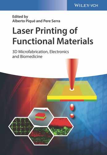
At NRL, this capability was demonstrated for the laser forward transfer of individual InGaN LED semiconductor substrates (250 µm × 350 μm) in bare-die form, that is, unpackaged, using a series of low fluence (≈150–200 mJ/cm2) 10 ns pulses from either excimer (248 nm) or YAG (355 nm) lasers [8]. Once laser transferred, the LEDs were electrically tested and their operation verified. This laser-driven pick-and-place of electronic devices named “lase-and-place” has been shown to be compatible not only with bare-die semiconductor devices but also with a wide range of devices and structures independent of their size, thickness, and mass as displayed in the image in Figure 18.2. The optical micrograph shows examples of various objects transferred into laser micromachined pockets on the surface of an ULTEM-1000 receiving substrate. They range from two types of structures (a polyimide laser micromachined gear and two silicon beams) to unpackaged semiconductor devices of various sizes (a LM555 timing chip and four InGaN LEDs) and illustrate the range and capabilities of lase-and-place. As reported by the NRL group and discussed in the following sections, the devices are not damaged upon laser illumination of their active surface and subsequent transfer demonstrating the ability of this LIFT technique to effectively provide a noncontact alternative to mechanical pick-and-place tools.
Figure 18.2 Optical micrograph showing an arbitrary arrangement of various types of components and parts all transferred onto a plastic substrate (ULTEM-1000) using “lase-and-place.” The artwork in the center corresponds to the laser transfer schematic and was laser-printed by LIFT of a silver metallic nanoink (see Chapter 4).
18.3 Process Dynamics
LIFT techniques offer a practical alternative to conventional, that is, mechanically driven, pick-and-place methods for release, transfer, placement, and/or embedding of different types of millimeter- to micrometer-sized structures such as MEMS and similar structures, solid interconnects, passive components, sensors, actuators, semiconductor bare dice, and optoelectronic devices onto any 2D or 3D surface. The concept is simple in principle: have each component mounted on a laser-transparent support using an intermediate support layer. Upon exposure to one or several laser pulses, the support layer releases the component, and in the process, the component moves away from the support. This mechanism, however, can be initiated through various laser-induced effects ranging from thermal heating to full ablation of the support layer. The Twente group was the first to systematically study this range of effects [9] and compare/contrast the thermal and ablative release mechanisms. Their analysis applied to the transfer of silicon substrates based on the assumption that the process was driven by the substrate's absorption of the laser radiation rather than the intermediate layer. Relying on heating or ablation of the silicon substrate can lead to its transfer but also can cause its damage. Despite their technique's narrow implementation (only with silicon substrates), this work demonstrated the potential of LIFT of devices as an alternative to pick-and-place tools and investigated how the laser parameters (wavelength, pulse length, energy, and spatial characteristics) together with the nature of the intermediate layer (various types of laser-transparent carrier tapes with thermal adhesive films) and the donor-to-receiving substrate gap influenced the transfers. The results of Karlitskaya's work showed that for their optimized configuration, that is, using laser pulses from a frequency-doubled Nd:YAG (λ = 532 nm, τ = 0.2 ms) with a laser-transparent tape/thermal adhesive layer as carrier for silicon substrates, transfers with low release velocities (<1 m/s) were possible. Their goal was to avoid damage of the substrate upon landing and reduced tumbling to improve placement accuracy. Their statistical analysis of the transferred silicon substrates showed that with a gap between the donor and receiving substrates of 0.2 mm, it was possible to obtain a placement accuracy of ±35 µm [7].
Although the thermal release showed the possibility of achieving reasonable placement precision, accuracies of the order of less than ±20 µm are required in order to compete with pick-and-place tools [10]. Given the fact that LIFT of devices involves the release of gases of much lower densities compared to the objects being launched, these processes are expected to be highly sensitive to the initial conditions. That is, small variations in the absorption mechanisms or even nonuniformities in the homogeneity and/or thickness of the support layer will lead to very unstable transfers with poor overall reproducibility, as observed by the Twente group with both their ablative- or thermal-mediated release from adhesive tapes. An alternative approach using a multilayer support comprising of a blistering polymer layer and a pressure-sensitive layer (PSA), known as thermomechanical selective laser-assisted die transfer (tmSLADT), has been reported to achieve better placement accuracy by a group at North Dakota State University [11]. This process uses a combination of a polyimide blistering layer (along the lines of the BA-LIFT process discussed in Chapter 5 of this book) with a spin-coated PSA layer to which 680 µm × 680 μm silicon tiles 65 µm thick are attached. UV laser pulses from a frequency tripled Nd:YVO4 (λ = 355 nm, τ = 30 ns) strike the polyimide layer forming a blister that causes the PSA layer to release the attached die. The process results in complete release and transfer of devices most of the times (transfer rates up to 93.5% were reported) with placement accuracy of ±25 µm on average and under optimized conditions [12]. The difficulties in transfer yield and part placement accuracy can be found in the choice of carrier layer. For example, the use of chip carrier tapes as release layers limits further optimization of the process, as evidenced by the results obtained by the University of Twente group due to the fact that these tapes do not exhibit the uniformity required by the LIFT process. Similarly, the multilayer approach explored by the group at North Dakota State University led to an unnecessarily complex carrier support that resulted in less than 100% transfer yields. Notwithstanding these results, it is possible to achieve 100% transfer yields with better than ±25 µm placement accuracy using a single carrier layer that fully absorbs the laser pulses, as described in the next section.
18.3.1 Lase-and-Place
The polymer sacrificial layer is critical for achieving reproducible release and transfer of a given structure or device during lase-and-place. In its simplest form, it needs to absorb the laser and decompose into volatile components with little or no residue left afterward. Given that many polymers decompose cleanly upon irradiation with UV laser pulses, their use in lase-and-place allows high reproducibility in the transfers. In fact, the polymers used to hold the components or devices in the donor substrate fulfill the same role as that of the dynamic release layer discussed in Chapter 3 of this book. In general, the use of polymer solutions applicable via spin coating such as photoresists, semiconductor wafer protective coatings, and polyimide precursors works well in conjunction with sources producing nanosecond pulses in the UV, that is, excimer or frequency-tripled diode-pumped solid-state lasers. When done correctly, the polymer absorbs the entire laser pulse and fully decomposes, leaving no residue on the device while shielding it from laser damage. This has been demonstrated by the NRL group for devices ranging in size from 0.1 to over 6 mm2 [8, 13–15].
Using stroboscopic imaging techniques, snapshots of the actual launch, release, and travel away from the donor substrate have been reported as shown in the sequence of micrographs in Figure 18.3a–c. These images can be used to calculate the velocity as a function of laser fluence, and the results are plotted in Figure 18.3d. From this data, it is clear that for a given laser fluence, the lighter components are transferred at a higher velocity compared to the heavier ones [8]. The solid line for the 1 mm2 device corresponds to a fit based on the following relationship [5]
where ν is the velocity, η is the fraction of available energy converted into kinetic energy, ![]() is the laser fluence,
is the laser fluence, ![]() is the ablation threshold of the sacrificial polymer layer, and
is the ablation threshold of the sacrificial polymer layer, and ![]() is the mass per unit area of the device. Note that the solid curve for the 2.6 mm × 2.6 mm ASIC bare dies is a visual aid and not a fit to the aforementioned formula. While (18.1) is reasonably consistent with the experimental results obtained with the 1 mm2 samples, the energy conversion efficiency η is not necessarily constant over a wide range of laser fluences due to numerous other mechanisms responsible for energy losses. In fact, only a very small fraction of the incident laser energy is converted into kinetic energy responsible for the release and launch of the part or device. However, near the fluence threshold of 150 mJ/cm2, this is sufficient to release a part with velocities of a few meters per second without causing damage during launch or upon landing on the receiving substrate.
is the mass per unit area of the device. Note that the solid curve for the 2.6 mm × 2.6 mm ASIC bare dies is a visual aid and not a fit to the aforementioned formula. While (18.1) is reasonably consistent with the experimental results obtained with the 1 mm2 samples, the energy conversion efficiency η is not necessarily constant over a wide range of laser fluences due to numerous other mechanisms responsible for energy losses. In fact, only a very small fraction of the incident laser energy is converted into kinetic energy responsible for the release and launch of the part or device. However, near the fluence threshold of 150 mJ/cm2, this is sufficient to release a part with velocities of a few meters per second without causing damage during launch or upon landing on the receiving substrate.

Figure 18.3 Stroboscopic micrographs showing three stages in the transfer of 1 mm × 1 mm Si substrates (laser pulse is ≈100 mJ/cm2). (a) shows the device prior to launch at  ; (b) shows the laser as it vaporizes the polymer layer at
  ; and (c) shows the device moving away at
  μs. (d) Plot of release velocity versus laser fluence for two different sizes (1 mm2 vs 6.8 mm2) of unpackaged devices (bare die). The line fitting the data points for the 1 mm2 substrates represents a fit to Eq. (18.1) in the text, while the line for the 2.6 mm × 2.6 mm ASIC bare die is only a guide to the eye.
The lase-and-place technique has also been used successfully to laser transfer ultrathin (≈10 µm) silicon substrates, which despite their fragility, can be inserted with extreme placement accuracy on the surface of an acceptor substrate without being damaged or fractured [13, 14]. This type of ultrathin devices are representative of the class of components required for next generation of RFID tags and other flexible electronic applications. Furthermore, with lase-and-place, it is possible to place devices next to each other with sufficient precision to fabricate assemblies or arrays of components. Figure 18.4 shows an image of five 1 mm × 1 mm ultrathin (9 µm thick) Si substrates, transferred next to each other along a grid and spaced 50 µm apart to demonstrate the device placement control achievable with lase-and-place. A few of the substrates exhibit minor rotation from the grid arrangement. However, the overall placement accuracy is of the order of ±25 µm, despite minor rotation and tilting-away from the transfer axis. In fact, fine-tuning the transfer laser parameters, adjusting the device ribbon-to-substrate gap, and increasing the polymer layer uniformity in the donor substrate can further improve the overall placement control and reproducibility. The image in this figure also shows that despite their very low thickness (<10 µm), these Si substrates were laser-transferred intact (no cracks or fractures). Finally, the combination of lase-and-place with self-assembly techniques provides another way to achieve precise placement. For example, the application of magnetic fields to trap and align magnetically susceptible devices onto a substrate has been reported for ultrathin chip placement by Kuran et al. [16].
The aforementioned results demonstrate that LIFT techniques can place individual structures or device over a given location with sufficient precision for applications involving component assembly. Furthermore, since the donor substrate onto which the devices are attached is optically transparent, registration and alignment of the device with the receiving substrate are rather straightforward and can be performed via machine vision. This process can be carried out at great speeds (>10 devices/s) with great lateral precision (<25 µm) for short travel distances away from the support (<0.2 mm). The following sections discuss the use of lase-and-place with structures and components of different sizes, shapes, and robustness. This is an important attribute since the ability to handle delicate parts, that is, ultrathin semiconductor bare die, as well as very robust and oversized structures, that is, SMD resistors can only be achieved with dedicated nozzle tips when using mechanical tools such as pick-and-place. The ease by which the lase-and-place process can be adjusted allows it to handle a wide range of components both in terms of shape, size, overall mass, and type of device without degrading their mechanical or electrical functionality, which is ideal for applications in printed electronics.
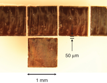
Figure 18.4 Optical micrograph showing transfers with lase-and-place of 1 mm × 1 mm ultrathin (9 µm thick) silicon die onto a glass receiving substrate with placement accuracy of ±25 µm and no signs of damage after laser transfer.
18.4 Laser Transfer of Intact Structures
As mentioned earlier, the original work by Holmes et al. demonstrated the use of LIFT to release prefabricated individual MEMS components held onto a donor substrate with a polymer sacrificial layer [4]. The laser-driven release of individual or multiple components is fast and is largely independent of geometry, size, or mass. This enables the fabrication of hybrid assemblies comprising a wide variety of structures, which cannot be produced using either chemically (wet) or plasma (dry) driven traditional etching techniques. As the transfers shown in Figure 18.2 show, the LIFT of whole structures can be applied to a broad range of shapes, sizes, and materials beyond silicon-based MEMS components. That is, the lase-and-place process works with structures made from silicon (bare die and beams), plastic (polyimide), and also metal (as discussed next).
Lase-and-place can also be applied to structures ranging in size from a few microns to millimeters as shown by the images in Figure 18.5. These results do not represent the technique's lower or upper limit for transferable sizes but rather illustrate its potential and versatility. As shown in Figure 18.5a, a 10 μm long, 200 nm diameter nickel nanorod was laser transferred without deformation or fracture above two posts etched on a silicon substrate. This capability offers great potential for the precise placement of discrete nanoscale structures, which would otherwise require handling via more complex and time-consuming techniques such as AFM-tips or laser tweezers. Patterned thin films can also be laser transferred as shown in Figure 18.5b, where a prepatterned 500 nm thick copper film 50 μm long by 10 μm wide was placed to form a bridge between two SU-8 pads. Alternatives for placing these relatively large but thin structures on a particular location on a substrate without damage can be found using self-assembly techniques. However, self-assembly becomes impractical when working with a few components of varying size requiring placement at arbitrary locations.
18.4.1 Laser Transfer of Metal Foils for Electrical Interconnects
Figure 18.5c,d shows much larger structures also handled by lase-and-place. The copper foils are 1 mm long and are attached with silver paste to the contact pads at the edges of the two devices for the purpose of serving as electrical interconnects. In general, wire bonding is the most common approach for fabricating interconnects. Wire bonding offers the greatest flexibility in terms of matching different device sizes, varying package form factors, and cost per interconnect. However, as circuits are implemented onto flexible substrates or 3D configurations, wire bonding is not practical given the large volume required to accommodate the wire loop as it connects from one pad to another [17]. Low profile, freestanding interconnects can be fabricated by dispensing conductive pastes or polymers [18]. These printed interconnects can accommodate flexing of the substrate, but given their composite nature (usually a mix of a polymer binder and metal particles), they are not well suited for handling high currents and their electrical performance degrades with time [19]. The laser transfer of copper foils allows the fabrication of low-profile interconnects as shown in Figure 18.5c which are much more robust and durable than printed inks or pastes.
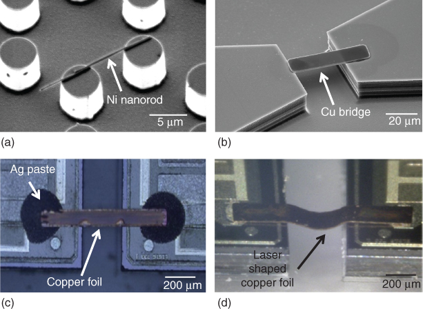
Figure 18.5 Images of representative structures transferred by lase-and-place. (a) SEM of nickel nanorod (200 nm diameter and 10 µm long) across silicon pods. (b) SEM of a copper film (10 µm wide, 50 µm long and 500 nm thick) over SU-8 pads. (c) Optical micrograph of a copper foil (150 µm wide, 1 mm long and 25 µm thick) connecting two capacitors using silver paste. (d) Similarly to (c), this time the copper foil was laser-shaped while attached to the donor substrate prior to its transfer.
The laser transfer of copper foils allows the fabrication of low-profile interconnects, but it does not address the challenges presented by flexible circuits where displacement of the devices due to flexing and thermal expansion mismatch can cause strains in the interconnects, which may cause their detachment or fracture, resulting in failure. It is thus necessary to consider alternatives to the simple flat geometries shown so far. One option explored by the NRL group is to use shaped metal beams that can flex in order to accommodate deflections under strain. An example of a laser-shaped copper beam is shown in the micrograph in Figure 18.5d where its placement over the pads of two individual devices with the shaped beam facing down between the devices is demonstrated for a low-profile yet flexible interconnect. Details on the fabrication, transfer and testing of these laser-shaped copper beams can be found in the work by Beniam et al. [20]. Overall, the ability to shape and print metal foils onto the pads of existing devices allows for low-profile interconnects of greater cross section, while minimizing the occupied volume. In wire bonding, especially on the ball bond side, the contact area between the wire and the die pad is ≈5 × 102 μm2. In contrast, the copper interconnect from a metal beam can have a contact area of ≈4 × 104 μm2 enabling lower contact resistance [20]. Overall, the use of flat or shaped metal beams or foils enables a new way to print low-profile, low-resistance, and mechanically compliant interconnects, which will play an important role in the development of next-generation flexible hybrid electronics comprising different types of electronic components, interconnects, and printed structures.
18.5 Laser Transfer of Components for Embedded Electronics
Embedded, that is, below the surface, passive components such as resistors, capacitors, and inductors have enjoyed widespread use for many years driven by high-density and high-speed applications. Current trends require the use of flexible substrates such as polyimide, polyester, or other polymer films, which allow the fabrication of thinner circuits capable of higher interconnect densities than traditional rigid substrates. The use of laser-based direct-write or LDW techniques offers an alternative for the fabrication of such embedded structures at a fraction of the cost and in less time than with traditional approaches, thus enabling the development of a full embedding capability for hybrid circuits.
In previous publications, the NRL group has demonstrated how LIFT techniques can be used to perform various circuit fabrication steps such as embedding the devices [14], laser transfer of individual devices into pockets on a substrate [13, 15], laser transfer of silver nanopastes to form 3D interconnects [21, 22] (see Chapter 10 for more details), and laser shaping and transfer of copper foils [20]. The objective of these reports was to investigate the use of laser processing techniques to carry out most of the steps required for the rapid prototyping of functional electronic circuits. By embedding bare die and unpackaged devices and wiring them using low-profile interconnects, significant reduction in thickness in the connections to the devices can be achieved with an overall reduction in footprint of about 80% and requiring substrates less than 1/10 of the thickness of a typical printed circuit board. If the savings from using bare die and other types of unpackaged devices are taken into consideration, volume reduction factors of 10–100 times, depending on the type of circuit design, become possible. Embedding components also result in shorter interconnects, which reduce parasitic inductance, thereby enhancing the electrical performance.
The use of laser microfabrication in combination with LIFT techniques to micromachine pockets, lase-and-place SMDs (resistors, capacitors, and LEDs) and bare die chips (i.e., a LM-555 timer chip), and laser transfer silver paste to form interconnects has been reported by NRL [23]. The steps required for laser fabricating a sample functional circuit in this manner are shown schematically in Figure 18.6a–c with micrographs from a sample circuit fabricated this way shown in Figure 18.6d–f. The circuit with planar interconnects shown in Figure 18.6f exemplifies the level of miniaturization achievable with footprints of less than 20% of that of existing layouts. This is illustrated by the insets in Figure 18.6f showing the actual size of the LIFT-fabricated circuit against a single packaged LM-555 chip (on the left) and details of the embedded LM-555 bare die showing the LIFT-printed interconnects (on the right). In principle, the same approach can be used to develop three-dimensional embedded circuits, where the components are placed at various depths or levels and their interconnects extend in 3D rather than 2D, so as to fully utilize the available space.

Figure 18.6 (a–c) Schematic (not to scale) showing the steps involved for LIFT of components and printing their interconnects for an embedded device. Optical micrographs of (d) an ULTEM 1000 substrate showing the laser-machined trenches, (e) the populated trenches with the blinker circuit components, including the LM-555 bare die in the center, and (f) the printed metal traces and interconnects for the embedded 555 blinker circuit. Bottom insets show the embedded circuit next to a packaged LM-555 chip for size comparison (left) and the LM-555 bare die and laser-printed interconnects (right)
18.6 Outlook
The need for implementing electronic systems that are compatible with additive manufacturing, 3D printing, and direct-write processes is pushing electronic manufacturing techniques beyond their current capabilities. In particular, traditional approaches to the manufacture of printed circuit boards are not compatible with the needs of a new generation of electronic systems that call for electronic circuits to be conformal, flexible, and hybrid in nature as the LED array made by laser transfer of bare-die LEDs on a polyimide foil in Figure 18.7a illustrates. Conformal circuits are needed to realize electronics in 3D rather than standard planar or 2D configurations, as shown in Figure 18.7b, a requirement that is becoming more urgent as 3D printed electronics mature and become more reliable. Flexible circuits require the integration of components into substrates or packages that are mechanically compliant so that they can conform, bend, stretch, or fold to a predesigned level without causing the circuit to fail. Hybrid circuits are comprised of distinct discrete components integrated into single or multilayer architectures assembled on nontraditional substrates as opposed to printed circuit boards. Examples of such components include logic, communication, memory, sensing, and power elements all integrated into a functional system or module. The need for new fabrication techniques capable of handling these new types of circuits cannot be ignored.
The design of such circuits will require the use of more sophisticated computer-based circuit layout tools, which will need to take into consideration issues such as power dissipation and stresses generated due to differences between the thermal expansion coefficients of the substrate and devices, in order to guarantee the circuit's long-term reliability. The implementation of such 3D circuit layouts represents a paradigm shift to the traditional planar approach to circuit manufacture and opens the possibility to further miniaturization and placement of electronics in locations considered impractical until now. Presently, the development of fully embedded electronic circuits has been limited at best, due to the lack of viable and practical fabrication techniques; however, the application of laser transfer techniques such as lase-and-place and other techniques for printed electronics will enable the development and implementation of fully functional 3D conformal electronic systems for applications ranging from distributed sensors to wearable devices.
From a circuit fabrication perspective, in order for any technique to be able to replace existing mechanically driven pick-and-place tools, it must be able to reliably place devices (i.e., with 100% transfer yields without damage) at the exact location with little variation (near-zero placement error) and precise orientation (little if any rotation). Furthermore, any new technique must be able to work with the new generation of small and ultrathin bare-die ICs. Finally, the technique in question must be capable of throughputs compatible with high-volume fabrication, meaning that device placement rates of over 10 components per second must be achievable. Manufacturers of mechanical pick-and-place tools are struggling to satisfy all these requirements, and the need for alternative processes cannot be ignored. The lase-and-place technique – LIFT-and-place maybe a better term – is capable of satisfying all these requirements, as described in the previous sections. Since it is laser-driven, it does not rely on the travel of pins or nozzles, which require translation stages constrained by mechanical acceleration/deacceleration limits. A laser beam can be pulsed and scanned at much higher rates, and the only mechanical movement required involves the alignment between the donor and receiving substrates, which can be greatly optimized to minimize acceleration/deacceleration steps. This noncontact feature is what enables lase-and-place to reach component transfer rates well above today's target of 10 devices/s and is perhaps the greatest advantage of the LIFT technique.
Other benefits of lase-and-place include cost reduction for prototyping and production, manufacture simplification (through the reduction of production steps), and greater design freedom due to the inherent geometrical versatility allowed by the laser transfer processes. LIFT of structures and functional devices offers a wide window of applications ranging from R&D and prototyping to high-throughput production. Many applications have already been identified with many more awaiting developments. However, many challenges for LIFT of hybrid electronics remain besides the establishment of design rules, such as process modeling and optimization, integrating and connecting large numbers of devices, metrology and evaluation of the performance of the printed patterns and circuits, and long-term reliability of the LIFT-made assemblies. Solving these challenges will require a considerable effort but as commercial applications develop and the electronics and aerospace industries embrace laser-based digital microfabrication processes, these issues will have to be addressed sooner or later. With increasing development and opportunities in micro- and mesosystems combining electronics, photonics, fluidics, and bioactivity, LIFT will play a significant role in the new paradigm offered by digital microfabrication.

Figure 18.7 Photos of a laser embedded array of LEDs on (a) a flexible polyimide substrate and (b) on an acrylic hemisphere.
18.7 Summary
The recent development of LIFT techniques for the transfer of preformed devices such as metal foils and functional devices such as semiconductor bare die opens the door for their use as unique tools for laser-based microelectronics fabrication. These lase-and-place systems will be capable of fabricating and embedding electronic circuits with their interconnects and printed conductive traces and perhaps even incorporate the required power storage and power harvesting components within the same substrate. The resulting fully integrated circuits could easily be reconfigured to fit within a desired form factor, thus allowing the placement of electronic systems in places inconceivable today.
As discussed in this chapter, laser-based device-transfer processes are a novel alternative to conventional mechanically driven pick-and-place methods for placement and embedding millimeter- to micrometer-sized structures such as semiconductor bare die, SMDs, optoelectronic devices, sensors, actuators, and MEMS onto any surface. Application of this technique to various types of semiconductor bare dies has shown that it is possible to transfer complete devices with the active surface facing the laser pulse without damage. This presents the device with its contact pads facing up, which greatly facilitates the printing or transfer of the metallic patterns required to connect it to the rest of the circuit using planar interconnects, thus replacing traditional wire bonding processes while minimizing space requirements. As the examples presented in this chapter demonstrate, the use of LIFT techniques allows the rapid prototyping of embedded microelectronics, which is not possible using current circuit board fabrication tools. In fact, the functionality of these laser-printed circuits could be customized for a particular application by choosing the appropriate electronic modules or building blocks from a circuit library available in the lase-and-place tool. Such a laser-based digital microfabrication system does not yet exist, but it is just a matter of time before LIFT-and-place tools are developed that make this vision a reality. Based on LIFT's success to date, it is highly probable that the laser-based printing techniques described in this chapter and the rest of this book will play a significant role in making embedded sensors and electronics and hybrid systems a reality in the not so distant future.
Acknowledgments
This work was funded by the Office of Naval Research (ONR) through the Naval Research Laboratory Basic Research Program.
References
- 1 Piqué, A., Mathews, S.A., Auyeung, R.C., Ollinger, M., Kim, H., Pratap, B., Arnold, C.B., and Sutto, T.E. (2004) Application of laser direct-write techniques for embedding electronic and micropower components. SPIE Proceedings, vol. 5662, pp. 564–569.
- 2 Piqué, A., Mathews, S.A., Auyeung, R.C., and Sood, B.P. (2011) Laser-based technique for the transfer and embedding of electronic components and devices. US Patent 8,056,222.
- 3 Piqué, A., Auyeung, R., Kim, H., Charipar, N., and Mathews, S. (2016) Laser 3D micro-manufacturing. J. Phys. D: Appl. Phys., 49 (22), 223001.
- 4 Holmes, A.S. and Saidam, S.M. (1998) Sacrificial layer process with laser-driven release for batch assembly operations. J. Microelectromech. Syst., 7 (4), 416–422.
- 5 Holmes, A.S. (2002) Laser processes for MEMS manufacture. SPIE Proceedings, vol. 4426, pp. 203–209.
- 6 Karlitskaya, N.S., Lange, D.F.D., Sanders, R., and Meijer, J. (2004) Study of laser die release by Q-switched Nd:YAG laser pulses. SPIE Proceedings, vol. 5448, pp. 935–943.
- 7 Karlitskaya, N.S., Meijer, J., Lange, D.F.D., and Kettelarij, H. (2006) Laser propulsion of microelectronic components: releasing mechanism investigation. SPIE Proceedings, vol. 6261, p. 62612P.
- 8 Mathews, S.A., Auyeung, R.C.Y., and Piqué, A. (2007) Use of laser direct-write in microelectronics assembly. J. Laser Micro/Nanoeng., 2 (1), 103–107.
- 9 Karlitskaya, N.S. (2011) Laser die transfer: laser-induced transfer of micro- components. PhD thesis. Faculty of Engineering Technology, University of Twente, The Netherlands.
- 10 Gilleo, K. (2004) Area Array Packaging Processes: For BGA, Flip Chip, and CSP, McGraw Hill Professional, New York.
- 11 Miller, R., Marinov, V., Swenson, O., Chen, Z., and Semler, M. (2012) Noncontact selective laser-assisted placement of thinned semiconductor dice. IEEE Trans. Compon. Packag. Manuf. Technol., 2 (6), 971–978.
- 12 Marinov, V., Swenson, O., Atanasov, Y., and Schneck, N. (2013) Laser-assisted ultrathin die packaging: insights from a process study. Microelectron. Eng., 101, 23–30.
- 13 Piqué, A., Charipar, N.A., Auyeung, R.C.Y., Kim, H., and Mathews, S.A. (2007) Assembly and integration of thin bare die using laser direct-write. SPIE Proceedings, vol. 6458, p. 645802.
- 14 Piqué, A., Charipar, N.A., Kim, H., Auyeung, R.C.Y., and Mathews, S.A. (2007) Applications of laser direct-write for embedding microelectronics. SPIE Proceedings, vol. 6606, p. 66060R.
- 15 Mathews, S.A., Charipar, N.A., Metkus, K., and Piqué, A. (2007) Manufacturing microelectronics using 'lase-and-place'. Photonics Spectra, 41 (10), 70–74.
- 16 Kuran, E., Berg, Y., Tichem, M., and Kotler, Z. (2015) Integration of laser die transfer and magnetic self-assembly for ultra-thin chip placement. J. Micromech. Microeng., 25 (4), 45 008.
- 17 Dixit, V., Davis, H., and Clark, M. ([Online]) Wire Bonding Considerations, http://electroiq.com/blog/2006/07/wire-bonding-considerations/ (accessed 24 February 2017).
- 18 Ahn, B.Y., Duoss, E.B., Motala, M.J., Guo, X., Park, S.I., Xiong, Y., Yoon, J., Nuzzo, R.G., Rogers, J.A., and Lewis, J.A. (2009) Omnidirectional printing of flexible, stretchable, and spanning silver microelectrodes. Science, 323 (5921), 1590–1593.
- 19 Perelaer, J., Smith, P.J., Mager, D., Soltman, D., Volkman, S.K., Subramanian, V., Korvink, J.G., and Schubert, U.S. (2010) Printed electronics: the challenges involved in printing devices, interconnects, and contacts based on inorganic materials. J. Mater. Chem., 20, 8446–8453.
- 20 Beniam, I., Mathews, S., Charipar, N., Auyeung, R., and Piqué, A. (2016) Laser printing of 3D metallic interconnects. SPIE Proceedings, vol. 9738, p. 97380I.
- 21 Wang, J., Auyeung, R., Kim, H., Charipar, N.A., and Piqué, A. (2010) Three-dimensional printing of interconnects by laser direct-write of silver nanopastes. Adv. Mater., 22 (40), 4462–4466.
- 22 Kim, H., Duocastella, M., Charipar, N.A., Auyeung, R.C.Y., and Piqué, A. (2013) Laser printing of conformal and multi-level 3D interconnects. Appl. Phys. A: Mater. Sci. Process., 113 (1), 5–8.
- 23 Piqué, A., Mathews, S.A., Pratap, B., Auyeung, R.C.Y., Karns, B.J., and Lakeou, S. (2006) Embedding electronic circuits by laser direct-write. Microelectron. Eng., 83 (11-12), 2527–2533.