
3
MICROPROCESSOR MEMORY ORGANIZATION
In this chapter we describe concepts associated with memory organization in typical microprocessors. Topics include main memory array design, memory management, and cache memory concepts.
3.1 Introduction
A memory unit is an integral part of any microcomputer, and its primary purpose is to hold instructions and data. The major design goal of a memory unit is to allow it to operate at a speed close to that of a microprocessor. However, the cost of a memory unit is so prohibitive that it is practically not feasible to design a large memory unit with one technology that guarantees high speed. Therefore, to seek a trade-off between the cost and the operating speed, a memory system is usually designed with different technologies, such as solid state, magnetic, and optical. In a broad sense, a microcomputer memory system can be divided into three groups:
1. Microprocessor memory
2. Primary or main memory
3. Secondary memory
Microprocessor memory comprises to a set of microprocessor registers. These registers are used to hold temporary results when a computation is in progress. Also, there is no speed disparity between these registers and the microprocessor because they are fabricated using the same technology. However, the cost involved in this approach limits a microcomputer architect to include only a few registers in the microprocessor.
Main memory is the storage area in which all programs are executed. The microprocessor can directly access only those items that are stored in main memory. Therefore, all programs must be within the main memory prior to execution. CMOS technology is normally used in main memory design. The size of the main memory is usually much larger than processor memory, and its operating speed is slower than that of processor registers. Main memory normally includes ROMs and RAMs.
Electromechanical memory devices such as hard disks are used extensively as microcomputer's secondary memory and allow storage of large programs at low cost. The storage capacity of a typical hard disk ranges from 5 MB to several gigabytes. The rotational speed of the hard disk is typically 3600 rpm. These secondary memory devices access stored data serially. Hence, they are significantly slower than main memory. Hard disk is a popular secondary memory device. Programs are stored on disks in files. Secondary memory stores programs in excess of the main memory. Secondary memory is also referred to as auxiliary or virtual memory. The microcomputer cannot execute programs stored in the secondary memory directly, so to execute these programs the microcomputer must transfer them to its main memory by a program called the operating system.

FIGURE 3.1 Main memory of the Pentium in the real mode.
Programs in hard disk memories are stored in tracks. A track is a concentric ring of programs stored on the surface of a disk. Each track is further subdivided into several sectors. Each sector typically stores 512 or 1024 bytes of information. The secondary memory typically uses magnetic media, except for optical memory, which stores programs on a plastic disk. CD (compact disc) memory and DVD (digital video disc) memory are examples of popular optical memory used with microcomputer systems. CD memory uses an infrared laser whereas DVD memory uses a red laser. Since a red laser has a shorter wavelength than an infrared laser, DVD memory provides a larger storage capacity than CD memory. Typical optical memories include CD-ROM, CD-RW, DVD-ROM, and DVD-RAM.
3.2 Main memory
The main or external memory (or simply, the memory) stores both instructions and data. For 8-bit microprocessors, the memory is divided into a number of 8-bit units called memory words. An 8-bit unit of data is termed a byte. Therefore, for an 8-bit microprocessor, memory word and memory byte mean the same thing. For 16-bit microprocessors, a word contains 2 bytes (16 bits). A memory word is identified in the memory by an address. For example, the Pentium microprocessor uses 32-bit addresses for accessing memory words. This provides a maximum of 232 = 4,294,964,296 = 4 GB of memory addresses, ranging from 0000000016 to FFFFFFFF16 in hexadecimal.
An important characteristic of a memory is whether it is volatile or nonvolatile. The contents of a volatile memory are lost if the power is turned off. On the other hand, a nonvolatile memory retains its contents after power is switched off. ROM is a typical example of nonvolatile memory. RAM is a volatile memory unless backed up by batteries.
Some microprocessors, such as the Intel Pentium, divide the memory into segments. For example, Pentium in the real mode divides the 1-MB main memory into 16 segments (0 through 15). Each segment contains 64 kB of memory and is addressed by 16 bits. Figure 3.1 shows a typical main memory layout of the Pentium in real mode. In the figure, the high 4 bits of an address specify the segment number. As an example, consider address 1000516 of segment 1. The high 4 bits, 0001, of this address define the location as in segment 1, and the low 16 bits, 000516, specify the particular address in segment 1. The 68000, on the other hand, uses linear or nonsegmented memory. For example, the 68000 uses 24 address pins to address 224= 16 MB of memory directly with addresses from 00000016 to FFFFFF16.

FIGURE 3.2 Summary of available semiconductor memories for microprocessor systems.
As mentioned before, memories can be categorized into two main types: read-only memory (ROM) and random-access memory (RAM). As shown in Figure 3.2, ROMs and RAMs are then divided into a number of subcategories, which are discussed next.
3.2.1 Read-Only Memory
ROMs can only be read, so is nonvolatile memory. CMOS technology is used to fabricate ROMs. ROMs are divided into two common types: mask ROM and erasable PROM (EPROM), such as 2732 and EAROM (electrically alterable ROM) [also called EEPROM or E2PROM (electrically erasable PROM)] such as the 2864.
Mask ROMs are programmed by a masking operation performed on a chip during the manufacturing process. The contents of mask ROMs are permanent and cannot be changed by the user. EPROMs can be programmed, and their contents can also be altered by using special equipment, called an EPROM programmer. When designing a microcomputer for a particular application, permanent programs are stored in ROMs. Control memories used to microprogram the control unit are ROMs.
EPROMs can be reprogrammed and erased. The chip must be removed from the microcomputer system for programming. This memory is erased by exposing the chip to ultraviolet light via a lid or window on the chip. Typical erase times vary between 10 and 20 min. The EPROM can be programmed by inserting the chip into a socket of the EPROM programmer and providing proper addresses and voltage pulses at the appropriate pins of the chip.
EAROMs can be programmed without removing the memory from the ROM's sockets. These memories are also called read-mostly memories (RMMs), because they have much slower write times than read times. Therefore, these memories are usually suited for operations when mostly reading rather that writing will be performed. Another type of memory, called Flash memory (nonvolatile), invented in the mid-1980s by Toshiba, is designed using a combination of EPROM and E2PROM technologies. Flash memory can be reprogrammed electrically while embedded on the board. One can change multiple bytes at a time. An example of flash memory is the Intel 28F020 (256K × 8-bit). Flash memory is typically used in cellular phones and digital cameras.
3.2.2 Random-Access Memory
There are two types of RAM: static RAM (SRAM), and dynamic RAM (DRAM). Static RAM stores data in flip-flops. Therefore, this memory does not need to be refreshed. RAMs are volatile unless backed up by battery. Dynamic RAM stores data in capacitors. That is, it can hold data for a few milliseconds. Hence, dynamic RAMs are refreshed typically by using external refresh circuitry. Dynamic RAMs (DRAMs) are used in applications requiring large memory. DRAMs have higher densities than static RAMs (SRAMs). Typical examples of DRAMs are the 4464 (64K × 4-bit), 44256 (256K × 4-bit), and 41000 (1M × 1-bit). DRAMs are inexpensive, occupy less space, and dissipate less power than SRAMs. Two enhanced versions of DRAM are EDO DRAM (extended data output DRAM) and SDRAM (synchronous DRAM).
The EDO DRAM provides fast access by allowing the DRAM controller to output the next address at the same time the current data is being read. An SDRAM contains multiple DRAMs (typically, four) internally. SDRAMs utilize the multiplexed addressing of conventional DRAMs. That is, like DRAMs, SDRAMs provide row and column addresses in two steps. However, the control signals and address inputs are sampled by the SDRAM at the leading edge of a common clock signal (133 MHz maximum). SDRAMs provide higher densities than conventional DRAMs by further reducing the need for support circuitry and faster speeds. The SDRAM has been used in PCs (personal computers).
3.2.3 READ and WRITE Timing Diagrams
To execute an instruction, the microprocessor reads or fetches the op-code via the data bus from a memory location in the ROM/RAM external to the microprocessor. It then places the op-code (instruction) in the instruction register. Finally, the microprocessor executes the instruction. Therefore, the execution of an instruction consists of two portions, instruction fetch and instruction execution. We consider the instruction fetch, memory READ, and memory WRITE timing diagrams in the following using a single clock signal. Figure 3.3 shows a typical instruction fetch timing diagram.
In Figure 3.3, to fetch an instruction, when the clock signal goes to HIGH, the microprocessor places the contents of the program counter on the address bus via address pins A0–A15 on the chip. Note that since each of lines A0–A15 can be either HIGH or LOW, both transitions are shown for the address in Figure 3.3. The instruction fetch is basically a memory READ operation. Therefore, the microprocessor raises the signal on the READ pin to HIGH. As soon as the clock goes to LOW, the logic external to the microprocessor gets the contents of the memory location addressed by A0–A15 and places them on the data bus D0–D7. The microprocessor then takes the data and stores it in the instruction register so that it gets interpreted as an instruction. This is called instruction fetch. The microprocessor performs this sequence of operations for every instruction.

FIGURE 3.3 Typical instruction fetch timing diagram for an 8-bit microprocessor.
We now describe the READ and WRITE timing diagrams. A typical READ timing diagram is shown in Figure 3.4. Memory READ is basically loading the contents of a memory location of the main ROM/RAM into an internal register of the microprocessor. The address of the location is provided by the contents of the memory address register (MAR). Let us now explain the READ timing diagram of Figure 3.4.
1. The microprocessor performs the instruction fetch cycle as before to READ the op-code.
2. The microprocessor interprets the op-code as a memory READ operation.
3. When the clock pin signal goes HIGH, the microprocessor places the contents of the memory address register on the address pins A0–Al5 of the chip.
4. At the same time, the microprocessor raises the READ pin signal to HIGH.
5. The logic external to the microprocessor gets the contents of the location in the main ROM/RAM addressed by the memory address register and places it on the data bus.
6. Finally, the microprocessor gets this data from the data bus via pins D0-D7 and stores it in an internal register.
Memory WRITE is basically storing the contents of an internal register of the microprocessor into a memory location of the main RAM. The contents of the memory address register provide the address of the location where data is to be stored. Figure 3.5 shows a typical WRITE timing diagram.
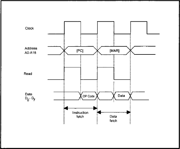
FIGURE 3.4 Typical memory READ timing diagram.
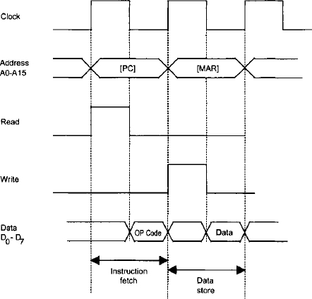
FIGURE 3.5 Typical memory WRITE timing diagram.
The microprocessor fetches the instruction code as before.
The microprocessor interprets the instruction code as a memory WRITE instruction and then proceeds to perform the DATA STORE cycle.
When the clock pin signal goes HIGH, the microprocessor places the contents of the memory address register on the address pins A0–A15 of the chip.
At the same time, the microprocessor raises the WRITE pin signal to HIGH.
The microprocessor places data to be stored from the contents of an internal register onto data pins D0–D7.
The logic external to the microprocessor stores the data from the register into a RAM location addressed by the memory address register.
3.2.4 Main Memory Organization
As mentioned earlier, microcomputer main memory typically consists of ROMs/EPROMs and RAMs. Because RAMs can be both read from and written into, the logic required to implement RAMs is more complex than ROMs/EPROMs. A microcomputer system designer is normally interested in how the microcomputer memory is organized or, in other words, how to connect the ROMS/EPROMs and RAMs and then determine the memory map of the microcomputer. That is, the designer would be interested in finding out what memory locations are assigned to the ROMs/ EPROMs and RAMs. The designer can then implement the permanent programs in ROMs/ EPROMs and the temporary programs in RAMs. Note that RAMs are needed when subroutines and interrupts requiring a stack are desired in an application.
As mentioned before, DRAMs (dynamic RAMs) use MOS capacitors to store information and need to be refreshed. DRAMs are less inexpensive than SRAMs, provide larger bit densities and consume less power. DRAMs are typically used when memory requirements are 16K words or larger. DRAM is addressed via row and column addressing. For example, 1-Mb (one megabit) DRAM requiring 20 address bits is addressed using 10 address lines and two control lines, ![]() (row address strobe) and
(row address strobe) and ![]() (column address strobe). To provide a 20-bit address into the DRAM, a LOW is applied to
(column address strobe). To provide a 20-bit address into the DRAM, a LOW is applied to ![]() and 10 bits of the address are latched. The other 10 bits of the address are applied next and
and 10 bits of the address are latched. The other 10 bits of the address are applied next and ![]() is then held LOW.
is then held LOW.
The addressing capability of the DRAM can be increased by a factor of 4 by adding one more bit to the address line. This is because one additional address bit results into one additional row bit and one additional column bit. This is why DRAMs can be expanded to larger memory very rapidly with the inclusion of additional address bits. External logic is required to generate the ![]() and
and ![]() signals and to output the current address bits to the DRAM.
signals and to output the current address bits to the DRAM.
DRAM controller chips take care of the refreshing and timing requirements needed by DRAMs. DRAMs typically require a 4-ms refresh time. The DRAM controller performs its task independent of the microprocessor. The DRAM controller chip sends a wait signal to the microprocessor if the microprocessor tries to access memory during a refresh cycle.
Because of the large memory, the address lines should be buffered using the 74LS244 or 74HC244 (a unidirectional buffer), and data lines should be buffered using the 74LS245 or 74HC245 (a bidirectional buffer) to increase the drive capability. Also, typical multiplexers such as 74LS157 or 74HC157 can be used to multiplex the microprocessors address lines into separate row and column addresses.
3.2.5 Main Memory Array Design
We noticed earlier that the main memory of a microcomputer is fabricated using solid-state technology. In a typical microcomputer application, a designer has to implement the required capacity by interconnecting several memory chips. This concept is known as memory array design. We address this topic in this section and show how to interface a memory system with a typical microprocessor.
Now let us discuss how to design ROM/RAM arrays. In particular, our discussion is focused on the design of memory arrays for a hypothetical microcomputer. The pertinent signals of a typical microprocessor necessary for main memory interfacing are shown in Figure 3.6. There are 16 address lines, A15-A0, with A0 being the least significant bit. This means that this microprocessor can address directly a maximum of 216 = 65,536 or 64K bytes of memory locations.
The control line ![]() goes LOW if the microprocessor executes an I/O instruction; it is held HIGH if the microprocessor executes a memory instruction. Similarly, the microprocessor drives control line
goes LOW if the microprocessor executes an I/O instruction; it is held HIGH if the microprocessor executes a memory instruction. Similarly, the microprocessor drives control line ![]() HIGH for READ operation; it is held LOW for WRITE operation. Note that all 16 address lines and the two control lines
HIGH for READ operation; it is held LOW for WRITE operation. Note that all 16 address lines and the two control lines ![]() described so far are unidirectional in nature; that is, information can always travel on these lines from the processor to external units. Eight bidirectional data lines, D7-D0 (with D0 being the least significant bit) are also shown in Figure 3.6. These lines are used to allow data transfer from the processor to external units, and vice versa.
described so far are unidirectional in nature; that is, information can always travel on these lines from the processor to external units. Eight bidirectional data lines, D7-D0 (with D0 being the least significant bit) are also shown in Figure 3.6. These lines are used to allow data transfer from the processor to external units, and vice versa.
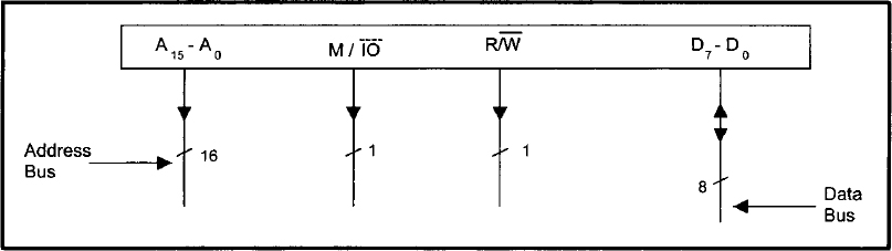
FIGURE 3.6 Pertinent signals of a typical microprocessor required for main memory interfacing.

FIGURE 3.7 Typical 1K × 8 SRAM chip.
In a typical application, the total amount of main memory connected to a microprocessor consists of a combination of ROMs and RAMs. However, in the following we illustrate for simplicity how to design memory array using only SRAM chips.
The pin diagram of a typical 1K × 8 RAM chip is shown in Figure 3.7. In this chip there are 10 address lines, A9-A0, so one can read or write 1024 (210 = 1024) different memory words. Also, in this chip there are eight bidirectional data lines, D7-D0 so that information can travel back and forth between the microprocessor and the memory unit. The three control lines ![]() , CS2, and
, CS2, and ![]() are used to control the SRAM unit according to the truth table shown in Table 3.1 from which it can be concluded that the RAM unit is enabled only when
are used to control the SRAM unit according to the truth table shown in Table 3.1 from which it can be concluded that the RAM unit is enabled only when ![]() and CS2 = 1. Under this condition,
and CS2 = 1. Under this condition, ![]() and
and ![]() imply write and read operations, respectively.
imply write and read operations, respectively.
To connect a microprocessor to ROM/RAM chips, two address-decoding techniques are commonly used: linear decoding and full decoding. Let us discuss first how to interconnect a microprocessor with a 4K SRAM chip array comprised of the four 1K SRAM chips of Figure 3.7 using the linear decoding technique. Figure 3.8 uses linear decoding to accomplish this. In this approach, address lines A9-A0 of the microprocessor are connected to all SRAM chips. Similarly, the control lines ![]() and
and ![]() of the microprocessor are connected to control lines CS2 and
of the microprocessor are connected to control lines CS2 and ![]() , respectively of each SRAM chip. The high-order address bits A10-Al3 act directly as chip selects. In particular, address lines A10 and A11 select SRAM chips I and II, respectively. Similarly, the address lines A12 and A13 select the SRAM chips III and IV, respectively. A15 and A14 are don't cares and are assumed to be zero. Table 3.2 describes how the addresses are distributed among the four 1K SRAM chips. The primary advantage this method, known as linear select decoding, is that it does not require decoding hardware. However, if two or more of lines A10-A13 are low at the same time, more than one SRAM chip are selected, and this causes a bus conflict.
, respectively of each SRAM chip. The high-order address bits A10-Al3 act directly as chip selects. In particular, address lines A10 and A11 select SRAM chips I and II, respectively. Similarly, the address lines A12 and A13 select the SRAM chips III and IV, respectively. A15 and A14 are don't cares and are assumed to be zero. Table 3.2 describes how the addresses are distributed among the four 1K SRAM chips. The primary advantage this method, known as linear select decoding, is that it does not require decoding hardware. However, if two or more of lines A10-A13 are low at the same time, more than one SRAM chip are selected, and this causes a bus conflict.
TABLE 3.1 Truth Table for Controlling SRAM.


FIGURE 3.8 Microprocessor connected to 4K SRAM using the linear select decoding technique.
Because of this potential problem, the software must be written such that it never reads into or writes from any address in which more than one of bits A13-A10 are low. Another disadvantage of this method is that it wastes a large amount of address space. For example, whenever the address value is B800 or 3800, SRAM chip I is selected. In other words, address 3800 is the mirror reflection of address B800 (this situation is also called memory foldback). This technique is therefore limited to a small system. The system of Figure 3.8 can be expanded up to a total capacity of 6K using A14 and A15 as chip selects for two more 1K SRAM chips.
TABLE 3.2 Address Map of the Memory Organization of Figure 3.8
| Address Range (Hex) | SRAM Chip Number |
| 3800-3BFF | I |
| 3400-37FF | II |
| 2C00-2FFF | III |
| 1C00-1FFF | IV |
To resolve problems with linear decoding, we use full decoded memory addressing. In this technique we use a decoder. The 4K memory system designed using this technique is shown in Figure 3.9. Note that the decoder in the figure is very similar to a practical decoder such as the 74LS138 with three chip enables. In Figure 3.9 the decoder output selects one of the four 1K SRAM chips, depending on the values of A12, A11, and A10 (Table 3.3).
Note that the decoder output will be enabled only when ![]() and E1 = 1. Therefore, in the organization of Figure 3.9, when any one of the high-order bits A15, A14, or A13 is 1, the decoder will be disabled, and thus none of the SRAM chips will be selected. In this arrangement, the memory addresses are assigned as shown in Table 3.4.
and E1 = 1. Therefore, in the organization of Figure 3.9, when any one of the high-order bits A15, A14, or A13 is 1, the decoder will be disabled, and thus none of the SRAM chips will be selected. In this arrangement, the memory addresses are assigned as shown in Table 3.4.
This approach does not waste any address space since the unused decoder outputs (don't cares) can be used for memory expansion. For example, the 3-to-8 decoder of Figure 3.9 can select eight 1K SRAM chips. Also, this method does not generate any bus conflict. This is because the decoder output selected ensures enabling of one memory chip at a time.
Finally, FPGAs can now be used with 32-bit microprocessors such as the Intel Pentium and Motorola 68020 for performing the memory decode function.
3.3 Microprocessor on-chip memory management unit and cache
Typical 32-bit microprocessors such as the Pentium contain on-chip memory management unit hardware and on-chip cache memory. These topics are discussed next.
3.3.1 Memory Management Concepts
Due to the massive amount of information that must be saved in most systems, the mass storage device is often a disk. If each access is to a hard disk, system throughput will be reduced to unacceptable levels. An obvious solution is to use a large and fast locally accessed semiconductor memory. Unfortunately, the storage cost per bit for this solution is very high. A combination of both off-board disk (secondary memory) and on-board semiconductor main memory must be designed into a system. This requires a mechanism to manage the two-way flow of information between the primary (semiconductor) and secondary (disk) media. This mechanism must be able to transfer blocks of data efficiently, keep track of block usage, and replace them in a nonarbitrary way. The main memory system must therefore be able to dynamically allocate memory space.
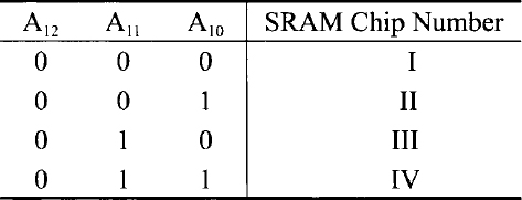

FIGURE 3.9 Interconnecting a microprocessor with a 4K RAM using full decoded memory addressing.
An operating system must have resource protection from corruption or abuse by users. Users must be able to protect areas of code from each other while maintaining the ability to communicate and share other areas of code. All these requirements indicate the need for a device, located between the microprocessor and memory, to control accesses, perform address mappings, and act as an interface between the logical (programmer's memory) and physical (microprocessor's directly addressable memory) address spaces. Because this device must manage the memory use configuration, it is appropriately called the memory management unit (MMU).
TABLE 3.4 Address Map of the Memory Organization of Figure 3.9.
| Address Range (Hex) | RAM Chip Number |
| 0000-03FF | I |
| 0400-07FF | II |
| 0800-0BFF | III |
| 0C00-0FFF | IV |

FIGURE 3.10 Address translation
Typical 32-bit processors such as the Motorola 68030/68040 and the Intel Pentium include on-chip MMUs. An MMU reduces the burden of the memory management function of the operating system. The basic functions provided by an MMU are address translation and protection. It translates logical program addresses to physical memory address. Note that in assembly language programming, addresses are referred to by symbolic names. These addresses in a program are called logical addresses because they indicate the logical positions of instructions and data. The MMU translates these logical addresses to physical addresses provided by the memory chips. The MMU can perform address translation in one of two ways:
1. By using the substitution technique [Figure 3.10(a)].
2. By adding an offset to each logical address to obtain the corresponding physical address [Figure 3.10(b)].
Address translation using the substitution technique is faster than translation using the offset method. However, the offset method has the advantage of mapping a logical address to any physical address as determined by the offset value.
Memory is usually divided into small manageable units. The terms page and segment are frequently used to describe these units. Paging divides the memory into equal-sized pages; segmentation divides the memory into variable-sized segments. It is relatively easier to implement the address translation table if the logical and main memory spaces are divided into pages.
There are three ways to map logical addresses to physical addresses: paging, segmentation, and combined paging-segmentation. In a paged system, a user has access to a larger address space than physical memory provides. The virtual memory system is managed by both hardware and software. The hardware included in the memory management unit handles address translation. The memory management software in the operating system performs all functions, including page replacement policies to provide efficient memory utilization. The memory management software performs functions such as removal of the desired page from main memory to accommodate a new page, transferring a new page from secondary to main memory at the right instant in time, and placing the page at the right location in memory.
If the main memory is full during transfer from secondary to main memory, it is necessary to remove a page from main memory to accommodate the new page. Two popular page replacement policies are first in first out (FIFO) and least recently used (LRU). The FIFO policy removes the page from main memory that has been resident in memory longest. The FIFO replacement policy is easy to implement, but one of its main disadvantages is that heavily used pages are likely to be replaced. Note that heavily used pages are resident in main memory longest. This replacement policy is sometimes a poor choice. For example, in a time-shared system, several users normally share a copy of the text editor in order to type and correct programs. The FIFO policy on such a system might replace a heavily used editor page to make room for a new page. This editor page might be recalled to main memory immediately. FIFO would be a poor choice in this case. The LRU policy, on the other hand, replaces the page that has not been used for the longest amount of time.
In the segmentation method, an MMU utilizes the segment selector to obtain a descriptor from a table in memory containing several descriptors. A descriptor contains the physical base address for a segment, the segment's privilege level, and some control bits. When the MMU obtains a logical address from the microprocessor, it first determines whether the segment is already in physical memory. If it is, the MMU adds an offset component to the segment base component of the address obtained from the segment descriptor table to provide the physical address. The MMU then generates the physical address on the address bus for selecting the memory. On the other hand, if the MMU does not find the logical address in physical memory, it interrupts the microprocessor. The microprocessor executes a service routine to bring the desired program from a secondary memory such as disk to the physical memory. The MMU determines the physical address using the segment offset and descriptor as described earlier and then generates the physical address on the address bus for memory. A segment will usually consist of an integral number of pages, each, say, 256 bytes long. With different-sized segments being swapped in and out, areas of valuable primary memory can become unusable. Memory is unusable for segmentation when it is sandwiched between already allocated segments and if it is not large enough to hold the latest segment that needs to be loaded. This is called external fragmentation and is handled by MMUs using special techniques. An example of external fragmentation is shown in Figure 3.11. The advantages of segmented memory management are that few descriptors are required for large programs or data spaces and that internal fragmentation (discussed later) is minimized. The disadvantages include external fragmentation, the need for involved algorithms for placing data, possible restrictions on the starting address, and the need for longer data swap times to support virtual memory.
Address translation using descriptor tables offers a protection feature. A segment or a page can be protected from access by a program section of a lower privilege level. For example, the selector component of each logical address includes 1 or 2 bits indicating the privilege level of the program requesting access to a segment. Each segment descriptor also includes 1 or 2 bits providing the privilege level of that segment. When an executing program tries to access a segment, the MMU can compare the selector privilege level with the descriptor privilege level. If the segment selector has the same or a higher privilege level, the MMU permits access. If the privilege level of the selector is lower than that of the descriptor, the MMU can interrupt the microprocessor, informing it of a privilege-level violation. Therefore, the indirect technique of generating a physical address provides a mechanism for protecting critical program sections in the operating system. Because paging divides the memory into equal-sized pages, it avoids the major problem of segmentation: external fragmentation. Because the pages are of the same size, when a new page is requested and an old one swapped out, the new one will always fit into the space vacated. However, a problem common to both techniques remains: internal fragmentation. Internal fragmentation is a condition where memory is unused but allocated due to memory block size implementation restrictions. This occurs when a module needs, say, 300 bytes and the page is 1 kB, as shown in Figure 3.12.
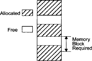
FIGURE 3.11 Memory fragmentation (external).
In the paged-segmentation method, each segment contains a number of pages. The logical address is divided into three components: segment, page, and word. The segment component defines a segment number, the page component defines the page within the segment, and the word component provides the particular word within the page. A page component of n bits can provide up to 2n pages. A segment can be assigned with one or more pages up to maximum of 2n pages; therefore, a segment size depends on the number of pages assigned to it.
A protection mechanism can be assigned to either a physical address or a logical address. Physical memory protection can be accomplished by using one or more protection bits with each block to define the access type permitted on the block. This means that each time a page is transferred from one block to another, the block protection bits must be updated. A more efficient approach is to provide a protection feature in logical address space by including protection bits in descriptors of the segment table in the MMU.
Virtual memory is the most fundamental concept implemented by a system that performs memory-management functions such as space allocation, program relocation, code sharing, and protection. The key idea behind this concept is to allow a user program to address more locations than those available in a physical memory. An address generated by a user program is called a virtual address. The set of virtual addresses constitutes the virtual address space. Similarly, the main memory of a microcomputer contains a fixed number of addressable locations, and a set of these locations forms the physical address space. The basic hardware for virtual memory is implemented in 32-bit microprocessors as an on-chip feature. These 32-bit processors support both cache and virtual memories. The virtual addresses are typically converted to physical addresses and then applied to cache.

FIGURE 3.12 Memory fragmentation (internal).
3.3.2 Cache Memory Organization
The performance of a microprocessor system can be improved significantly by introducing a small, expensive, but fast memory between the microprocessor and main memory. The idea for cache memory was introduced in the IBM 360/85 computer. Later, the concept was implemented in minicomputers such as the PDP-11/70. With the advent of very large scale integration (VLSI) technology, the cache memory technique has been gaining acceptance in the microprocessor world. Studies have shown that typical programs spend most of their execution time in loops. This means that the addresses generated by a microprocessor have a tendency to cluster around a small region in the main memory, a phenomenon known as locality of reference. Typical 32-bit microprocessors can execute the same instructions in a loop from the on-chip cache rather than reading them repeatedly from the external main memory. Thus, the performance is greatly improved. For example, an on-chip cache memory is implemented in Intel's 32-bit microprocessor, the 80486/Pentium, and Motorola's 32-bit microprocessor, the 68030/68040. The 80386 does not have an on-chip cache, but external cache memory can be interfaced to it.
A block diagram representation of a microprocessor system that employs a cache memory is shown in Figure 3.13. Usually, a cache memory is very small in size and its access time is less than that of the main memory by a factor of 5. Typically, the access times of the cache and main memories are 100 and 500 ns, respectively. If a reference is found in the cache, we call it a cache hit, and the information pertaining to the microprocessor reference is transferred to the microprocessor from the cache. However, if the reference is not found in the cache, we call it a cache miss.
When there is a cache miss, the main memory is accessed by the microprocessor and the instructions and/or data are transferred to the microprocessor from the main memory. At the same time, a block containing the information needed by the microprocessor is transferred from the main memory to cache. The block normally contains 4 to 16 words, and this block is placed in the cache using standard replacement policies such as FIFO or LRU. This block transfer is done with the hope that all future references made by the microprocessor will be confined to the fast cache.
The relationship between the cache and main memory blocks is established using mapping techniques. Three widely used mapping techniques are direct mapping, fully associative mapping, and set-associative mapping. To explain these three mapping techniques, the memory organization of Figure 3.14 will be used. The main memory is capable of storing 4K words of 16 bits each. The cache memory, on the other hand, can store 256 words of 16 bits each. An identical copy of every word stored in cache exists in main memory. The microprocessor first accesses the cache. If there is a hit, the microprocessor accepts the 16-bit word from the cache. In case of a miss, the microprocessor reads the desired 16-bit word from the main memory, and this 16-bit word is then written to the cache. A cache memory may contain instructions only (Instruction cache) or data only (data cache) or both instructions and data (unified cache).
Direct mapping uses a RAM for the cache. The microprocessor's 12-bit address is divided into two fields, an index field and a tag field. Because the cache address is 8 bits wide (28 = 256), the low-order 8 bits of the microprocessor's address form the index field, and the remaining 4 bits constitute the tag field. This is illustrated in Figure 3.15.
In general, if the main memory address field is m bits wide and the cache memory address is n bits wide, the index field will then require n bits and the tag field will be (m - n) bits wide. The n-bit address will access the cache. Each word in the cache will include the data word and its associated tag. When the microprocessor generates an address for main memory, the index field is used as the address to access the cache. The tag field of the main memory is compared with the tag field in the word read from cache. A hit occurs if the tags match. This means that the data word desired is in cache. A miss occurs if there is no match, and the required word is read from main memory. It is written in the cache along with the tag. One of the main drawbacks of direct mapping is that numerous misses may occur if two or more words with addresses that have the same index but different tags are accessed several times. This situation should be avoided or can be minimized by having such words far apart in the address lines.

FIGURE 3.13 Memory organization of a microprocessor system that employs a cache memory.
Let us illustrate the concept of direct mapping for a data cache by means of the numerical example shown in Figure 3.15. All numbers are in hexadecimal. The content of index address 00 of cache is tag = 0 and data = 013F. Suppose that a microprocessor wants to access the memory address 100. The index address 00 is used to access the cache. Memory address tag 1 is compared with cache tag 0. This does not produce a match. Therefore, the main memory is accessed and the data 2714 is transferred into the microprocessor. The cache word at index address 00 is then replaced by a tag of 1 and data of 2714.
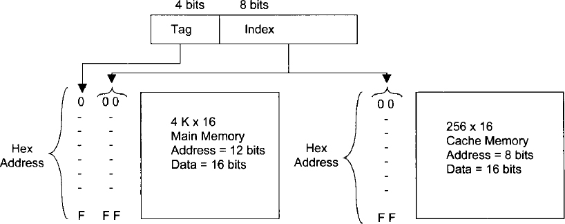
FIGURE 3.14 Addresses for main and cache memory.

FIGURE 3.15 Direct mapping numerical example.
The fastest and most expensive cache memory known as fully associative mapping utilizes an associative memory. Each element in associative memory contains a main memory address and its content (data). When the microprocessor generates a main memory address, it is compared associatively (simultaneously) with all addresses in the associative memory. If there is a match, the corresponding data word is read from the associative cache memory and sent to the microprocessor. If a miss occurs, the main memory is accessed and the address and its corresponding data are written to the associative cache memory. If the cache is full, certain policies such as FIFO, are used as replacement algorithms for the cache. Associative cache is expensive but provides fast operation. The concept of associative cache is illustrated by means of a numerical example in Figure 3.16. Assume that all numbers are hexadecimal.
The associative memory stores both the memory address and its contents (data). The figure shows four words stored in the associative cache. Each word in the cache is a 12-bit address along with its 16-bit contents (data). When the microprocessor wants to access memory, the 12-bit address is placed in an address register and the associative cache memory is searched for a matching address. Suppose that the content of the microprocessor address register is 445. Because there is a match, the microprocessor reads the corresponding data 0FA1 into an internal data register.
Set-associative mapping is a combination of direct and associative mapping. Each cache word stores two or more main memory words using the same index address. Each main memory word consists of a tag and its data word. An index with two or more tags and data words forms a set.

FIGURE 3.16 Numerical example of associative mapping.
When the microprocessor generates a memory request, the index of the main memory address is used as the cache address. The tag field of the main memory address is then compared associatively (simultaneously) with all tags stored under the index. If a match occurs, the desired dataword is read. If a match does not occur, the data word, along with its tag, is read from main memory and written into the cache. The hit ratio improves as the set size increases because more words with the same index but different tags can be stored in the cache.
The concept of set-associative mapping can be illustrated by the numerical example shown in Table 3.5. Assume that all numbers are hexadecimal. Each cache word can store two or more memory words under the same index address. Each data item is stored with its tag. The size of a set is defined by the number of tag and data items in a cache word. A set size of 2 is used in this example. Each index address contains two data words and their associated tags. Each tag includes 4 bits, and each data word contains 16 bits. Therefore, the word length = 2 × (4 + 16) = 40 bits. An index address of 8 bits can represent 256 words. Hence, the size of the cache memory is 256 × 40. It can store 512 main memory words because each cache word includes two data words.
The hex numbers shown in Table 3.5 are obtained from the main memory contents shown in Figure 3.15. The words stored at addresses 000 and 200 of main memory in Figure 3.15 are stored in cache memory (shown in Table 3.5) at index address 00. Similarly, the words at addresses 101 and 201 are stored at index address 01. When the microprocessor wants to access a memory word, the index value of the address is used to access the cache. The tag field of the microprocessor address is then compared with both tags in the cache associatively (simultaneously) for a cache hit. If there is a match, appropriate data is read into the microprocessor. The hit ratio will improve as the set size increases because more words with the same index but different tags can be stored in the cache. However, this may increase the cost of comparison logic.
TABLE 3.5 Numerical Example of Set-Associative Mapping with a Set Size of 2

There are two ways of writing into cache: the write-back and write-through methods. In the write-back method, whenever the microprocessor writes something into a cache word, a “dirty” bit is assigned to the cache word. When a dirty word is to be replaced with a new word, the dirty word is first copied into the main memory before it is overwritten by the incoming new word. The advantage of this method is that it avoids unnecessary writing into main memory.
In the write-through method, whenever the microprocessor alters a cache address, the same alteration is made in the main memory copy of the altered cache address. This policy is easily implemented and ensures that the contents of the main memory are always valid. This feature is desirable in a multiprocesssor system, in which the main memory is shared by several processors. However, this approach may lead to several unnecessary writes to main memory.
One of the important aspects of cache memory organization is to devise a method that ensures proper utilization of the cache. Usually, the tag directory contains an extra bit for each entry, called a valid bit. When the power is turned on, the valid bit corresponding to each cache block entry of the tag directory is reset to zero. This is done to indicate that the cache block holds invalid data. When a block of data is transferred from the main memory to a cache block, the valid bit corresponding to this cache block is set to 1. In this arrangement, whenever the valid bit is zero, it implies that a new incoming block can overwrite the existing cache block. Thus, there is no need to copy the contents of the cache block being replaced into the main memory.
The growth in integrated circuit (IC) technology has allowed manufacturers to fabricate a cache on a microprocessor chip such as Motorola's 32-bit microprocessor, the 68020. The 68020 on-chip cache is a direct-mapped instruction cache. Only instructions are cached; data items are not.
Finally, microprocessors such as the Intel Pentium II support two levels of cache, L1 (level 1) and L2 (level 2) cache memories. The L1 cache (smaller in size) is contained inside the processor chip while the L2 cache (larger in size) is interfaced external to the microprocessor. The L1 cache normally provides separate instruction and data caches. The processor can access the L1 cache directly and the L2 cache normally supplies instructions and data to the L1 cache. The L2 cache is usually accessed by the microprocessor only if LI misses occur. This two-level cache memory enhances microprocessor performance.
Questions and Problems
| 3.1 | What is the basic difference between main memory and secondary memory? |
| 3.2 | A microprocessor has 24 address pins. What is the maximum size of the main memory? |
| 3.3 | Can the microprocessor execute programs directly in hard disk? Explain your answer. |
| 3.4 | What is the basic difference between: (a) EPROM and EEPROM? (b) SRAM and DRAM? |
| 3.5 | Given a memory with a 14-bit address and an 8-bit word size.
|
| 3.6 | What are the main differences between CD and DVD memories? |
| 3.7 | Draw a block diagram showing the address and data lines for the 2732, and 2764 EPROM chips. |
| 3.8 | (a) How many address and data lines are required for a 1M × 16 memory chip?
(b) What is the size of a decoder with one chip enable |
| 3.9 | A microprocessor with 24 address pins and eight data pins is connected to a 1K × 8 memory chip with one chip enable. How many unused address bits of the microprocessor are available for interfacing other 1K × 8 memory chips? What is the maximum directly addressable memory available with this microprocessor? |

| 3.10 | Name the methods used in main memory array design. What are the advantages and disadvantages of each? |
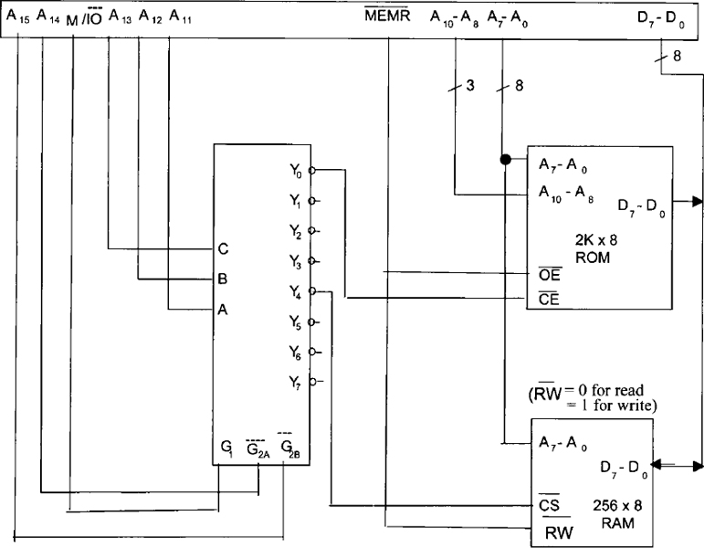
| 3.11 | The block diagram of a 512 × 8 RAM chip is shown in Figure P3.11. In this arrangement the memory chip is enabled only when |
| 3.12 | Consider the hardware schematic shown in Figure P3.12.
|

| 3.13 | Interface a microprocessor with 16-bit address pins and 8-bit data pins and a Assume that both EPROM and RAM chips contain two enable pins: |
| 3.14 | Repeat Problem 3.13 to obtain the memory map shown in Table P3.14 using a 74138 decoder. |
| 3.15 | What is meant by foldback in linear decoding? |
| 3.16 | Comment on the importance of the following features in an operating system implementation:
|
| 3.17 | Explain briefly the differences between segmentation and paging. |
| 3.18 | What is the advantage of having a cache memory? Name a 32-bit microprocessor that does not contain an on-chip cache. |
| 3.19 | What basic functions are performed by a microprocessor's on-chip MMU? |
| 3.20 | Discuss briefly the various cache-mapping techniques. |
| 3.21 | A microprocessor has a main memory of 8K × 32 and a cache memory of 4K × 32. Using direct mapping, determine the sizes of the tag field, index field, and each word of the cache. |
| 3.22 | A microprocessor has a main memory of 4K × 32. Using a cache memory address of 8 bits and set-associative mapping with a set size of 2, determine the size of the cache memory. |
| 3.23 | A microprocessor can address directly 1 MB of memory with a 16-bit word size. Determine the size of each cache memory word for associative mapping. |
| 3.24 | Under what conditions does the set-associative mapping method become one of the following?
|