
1
INTRODUCTION TO MICROPROCESSORS
Digital systems are designed to store, process, and communicate information in digital form. They are found in a wide range of applications, including process control, communication systems, digital instruments, and consumer products. A digital computer, more commonly called simply a computer, is an example of a typical digital system.
A computer manipulates information in digital or more precisely, binary form. A binary number has only two discrete values: zero or one. Each discrete value is represented by the OFF and ON status of an electronic switch called a transistor. All computers understand only binary numbers. Any decimal number (base 10, with ten digits from 0 to 9) can be represented by a binary number (base 2, with digits 0 and 1).
The basic blocks of a computer are the central processing unit (CPU), the memory, and the input/output (I/O). The CPU of a computer is basically the same as the brain of a human being; so computer memory is conceptually similar to human memory. A question asked of a human being is analogous to entering a program into a computer using an input device such as a keyboard, and a person answering a question is similar in concept to outputting the program result to a computer output device such as a printer. The main difference is that human beings can think independently, whereas computers can only answer questions for which they are programmed. Computer hardware includes such components as memory, CPU, transistors, nuts, bolts, and so on. Programs can perform a specific task, such as addition, if the computer has an electronic circuit capable of adding two numbers. Programmers cannot change these electronic circuits but can perform tasks on them using instructions.
Computer software consists of a collection of programs that contain instructions and data for performing a specific task. All programs, written using any programming language (e.g., C++), must be translated into binary prior to execution by a computer because the computer understands only binary numbers. Therefore, a translator is necessary to convert such a program into binary and this is achieved using a translator program called a compiler. Programs in the binary form of 1's and 0's are then stored in the computer memory for execution. Also, as computers can only add, all operations, including subtraction, multiplication, and division, are performed by addition.
Due to advances in semiconductor technology, it is possible to fabricate a CPU on a single chip. The result is a microprocessor. Both metal-oxide semiconductor (MOS) and bipolar technologies are used in the fabrication process. The CPU can be placed on a single chip when MOS technology is used. However, several chips are required with bipolar technology. At present, HCMOS (high-speed complementary MOS) or BICMOS (combination of bipolar and HCMOS) technology is normally used to fabricate a microprocessor on a single chip. Along with the microprocessor chip, appropriate memory and I/O chips can be used to design a microcomputer. The pins on each one of these chips can be connected to the proper lines on a system bus, which consists of address, data, and control lines. In the past, some manufacturers designed a complete microcomputer on a single chip with limited capabilities. Single-chip microcomputers were used in a wide range of industrial and home applications.
Microcontrollers evolved from single-chip microcomputers. Microcontrollers are typically used for dedicated applications such as automotive systems, home appliances, and home entertainment systems. Typical microcontrollers include a microcomputer, timers, and A/D (analog-to- digital) and D/A (digital to analog) converters, all on a single chip. Examples of typical microcontrollers are the Intel 8751 (8-bit)/8096 (16-bit), Motorola HC11 (8-bit)/HC16 (16-bit), and Microchip Technology's PIC (peripheral interface controller).
In this chapter we first define some basic terms associated with microprocessors. We then describe briefly the evolution of microprocessors and typical features of 32- and 64-bit microprocessors. Finally, microprocessor-based system design concepts and typical microprocessor applications are included.
1.1 Explanation of Terms
Before we go on, it is necessary to understand some basic terms.
- An Address is a pattern of 0's and 1's that represents a specific location in memory or a particular I/O device. Typical 8-bit microprocessors have 16 address lines, and, these 16 lines can produce 216 unique 16-bit patterns from 0000000000000000 to 1111111111111111, representing 65,536 different address combinations.
- Addressing mode is the manner in which the microprocessor determines the operand (data) and destination addresses during execution of an instruction.
- An Arithmetic-logic unit (ALU) is a digital circuit that performs arithmetic and logic operations on two n-bit digital words. The value of n can be 4, 8, 16, 32, or 64. Typical operations performed by an ALU are addition, subtraction, ANDing, ORing, and comparison of two n-bit digital words. The size of the ALU defines the size of the microprocessor. For example, a 32-bit microprocessor contains a 32-bit ALU.
- Bit is an abbreviation for the term binary digit. A binary digit can have only two values, which are represented by the symbols 0 and 1, whereas a decimal digit can have 10 values, represented by the symbols 0 through 9. The bit values are easily implemented in electronic and magnetic media by two-state devices whose states portray either of the binary digits 0 and 1. Examples of such two-state devices are a transistor that is conducting or not conducting, a capacitor that is charged or discharged, and a magnetic material that is magnetized north to south or south to north.
- Bit size refers to the number of bits that can be processed simultaneously by the basic arithmetic circuits of a microprocessor. A number of bits taken as a group in this manner is called a word. For example, a 32-bit microprocessor can process a 32-bit word. An 8-bit word is referred to as a byte, and a 4-bit word is known as a nibble.
- A bus consists of a number of conductors (wires) organized to provide a means of communication among different elements in a microprocessor system. The conductors in a bus can be grouped in terms of their functions. A microprocessor normally has an address bus, a data bus, and a control bus. Address bits are sent to memory or to an external device on the address bus. Instructions from memory, and data to/from memory or external devices, normally travel on the data bus. Control signals for the other buses and among system elements are transmitted on the control bus. Buses are sometimes bidirectional; that is, information can be transmitted in either direction on the bus, but normally in only one direction at a time.
- Cache Memory is a high-speed, directly accessible, relatively small, semiconductor read/write memory block used to store data/instructions that the microprocessor may need in the immediate future. It increases speed by reducing the number of external memory reads required by the microprocessor. Typical 32-bit microprocessors such as the Intel Pentium are provided with on-chip cache memory. Pentium II supports two levels of cache. These are L1 (Level 1 cache) and L2 (Level 2 cache) cache memories. The L1 cache (smaller in size) is contained inside the microprocessor while L2 cache (larger in size) is interfaced to the microprocessor. This two level cache enhances the performance of the microprocessor.
- A Complex Instruction Set Computer (CISC) contains a large instruction set. It is difficult to pipeline compared to RISC. Motorola 68020 is a CISC microprocessor.
- Clock is analogous to human heart beats. The microprocessor requires synchronization among its components, and this is provided by a clock or timing circuits.
- The instruction set of a microprocessor is a list of commands that the microprocessor is designed to execute. Typical instructions are ADD, SUBTRACT, and STORE. Individual instructions are coded as unique bit patterns which are recognized and executed by the microprocessor. If a microprocessor has 3 bits allocated to the representation of instructions, the microprocessor will recognize a maximum of 23, or eight, different instructions. The microprocessor will then have a maximum of eight instructions in its instruction set. It is obvious that some instructions will be more suitable than others to a particular application. For example, if a microprocessor is to be used in a calculating mode, instructions such as ADD, SUBTRACT, MULTIPLY, and DIVIDE would be desirable. In a control application, instructions inputting digitized signals to the processor and outputting digital control variables to external circuits are essential. The number of instructions necessary in an application will directly influence the amount of hardware in the chip set and the number and organization of the interconnecting bus lines.
- Memory Management Unit (MMU) allows programmers to write programs much larger than could fit in the main memory space available to the microprocessor. The programs are simply stored in a secondary device such as a hard disk and portions of the programs are swapped into the main memory as needed for execution by the microprocessor. The MMU is implemented as on-chip hardware in typical microprocessors such as the Pentium.
- A microprocessor is the CPU of a microcomputer contained on a single chip, and must be intefaced with peripheral support chips in order to function. In general, a CPU contains several registers (memory elements), an ALU, and a control unit. Note that the control unit translates instructions and performs the desired task. The number of peripheral devices depends on the particular application involved and may even vary within an application. As the microprocessor industry matures, more of these functions are being integrated onto chips, to reduce the system package count. In general, a microcomputer typically consists of a microprocessor (CPU) chip, input and output chips, and memory chips in which programs (instructions and data) are stored. Note that a microcontroller, on the other hand, is implemented on a single chip containing typically a CPU, memory, I/O, a timer, and A/D and D/A converter circuits.
- Pipelining is a technique that overlaps instruction fetch (instruction read) with execution. This allows a microprocessor's processing operation to be broken down into several steps (dictated by the number of pipeline levels or stages) so that the individual step outputs can be handled by the microprocessor in parallel. Pipelining is often used to fetch the microprocessor's next instruction while executing the current instruction, which speeds up the overall operation of the microprocessor considerably.
- Random-access memory (RAM) is a storage medium for groups of bits or words whose contents cannot only be read but can also be altered at specific addresses. A RAM normally provides volatile storage, which means that its contents are lost in case power is turned off. RAMs are fabricated on chips and have typical densities of 4096 bits to 1 megabit per chip. These bits can be organized in many ways: for example, as 4096-by-1-bit words or as 2048-by-8-bit words. RAMs are normally used for the storage of temporary data and intermediate results as well as programs that can be reloaded from a backup nonvolatile source. RAMs are capable of providing large storage capacity, in the megabit range.
- Read-only memory (ROM) is a storage medium for the groups of bits called words, and its contents cannot normally be altered once programmed. A typical ROM is fabricated on a chip and can store, for example, 2048 eight-bit words, which can be accessed individually by presenting to it one of 2048 addresses. This ROM is referred to as a 2K by 8-bit ROM. 10110111 is an example of an 8-bit word that might be stored in one location in this memory. A ROM is a nonvolatile storage device, which means that its contents are retained in case power is turned off. Because of this characteristic, ROMs are used to store programs (instructions and data) that must always be available to the microprocessor.
- A register can be considered as volatile storage for a number of bits. These bits may be entered into the register simultaneously (in parallel) or sequentially (serially) from right to left or from left to right, 1 bit at a time. An 8-bit register storing the bits 11110000 is represented as follows:

- A reduced instruction set computer (RISC) contains a simple instruction set. The RISC architecture maximizes speed by reducing clock cycles per instruction and makes it easier to implement pipelining. A Power PC is a RISC microprocessor.
- A Superscalar microprocessor is provided with more than one pipeline and can execute more than one instruction per clock cycle. The Pentium is a superscalar microprocessor.
1.2 Microprocessor Data Types
In this section we discuss data types used by typical microprocessors: unsigned and signed binary numbers, binary-coded decimal (BCD), ASCII (American Standard Code for Information Interchange), EBCDIC (extended binary coded decimal interchange code), and floating-point numbers.
1.2.1 Unsigned and Signed Binary Numbers
An Unsigned binary number has no arithmetic sign, therefore, are always positive. Typical examples are your age or a memory address, which are always positive numbers. An 8-bit unsigned binary integer represents all numbers from 0016 through FF16(010 through 25510).
A signed binary number, on the other hand, includes both positive and negative numbers. It is represented in the microprocessor in two's-complement form. For example, the decimal number +15 is represented in 8-bit two's-complement form as 0000 1111 (binary) or 0F (hexadecimal). The decimal number −15 can be represented in 8-bit two's-complement form as 11110001 (binary) or F1 (hexadecimal). Also, the most significant bit (MSB) of a signed number represents the sign of the number. For example, bit 7 of an 8-bit number, bit 15 of a 16-bit number, and bit 31 of a 32-bit number represent the signs of the respective numbers. A “0” at the MSB represents a positive number; a “1” at the MSB represents a negative number. Note that the 8-bit binary number 11111111 is 25510 when represented as an unsigned number. On the other hand, 111111112 is −110 when represented as a signed number.
An error (indicated by overflow in a microprocessor) may occur while performing twos complement arithmetic. The microprocessor automatically sets an overflow bit to 1 if the result of an arithmetic operation is too big for the microprocessor's maximum word size; otherwise it is reset to 0. For signed arithmetic operations such as addition, the overflow, ![]() where Cf is the final carry and Cp is the previous carry. This can be illustrated by the following examples.
where Cf is the final carry and Cp is the previous carry. This can be illustrated by the following examples.
Consider the following examples for 8-bit numbers. Let Cf be the final carry (carry out of the most significant bit or sign bit) and Cp be the previous carry (carry out of bit 6 or seventh bit). We will show by means of numerical examples that as long as Cf and Cp are the same, the result is always correct. If, however, Cf and Cp are different, the result is incorrect and sets the overflow bit to 1. Now, consider the following cases.
Case 1: Cf and Cp are the same.
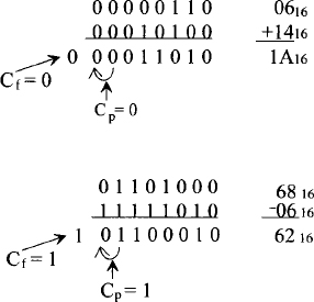
Therefore when Cf and Cp are either both 0 or both 1, a correct answer is obtained.
Case 2: Cf and Cp are different.

Cf = 0 and Cp = 1 give an incorrect answer because the result shows that the addition of two positive numbers is negative.
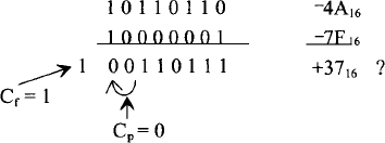
Cf = 1 and Cp = 0 provide an incorrect answer because the result indicates that the addition of two negative numbers is positive. Hence, the overflow bit will be set to zero if the carries Cf and Cp are the same, that is, if both Cf and Cp are either 0 or 1. On the other hand, the overflow flag will be set to 1 if carries Cf and Cp are different. The relationship among Cf, Cp, and V can be summerized in a truth table as follows:

From the truth table, overflow, ![]()
Note that the symbol ![]() represents exclusive-OR logic operation. Exclusive-OR means that when two inputs are the same (both one or both zero), the output is zero. On the other hand, if two inputs are different, the output is one. The overflow can be considered as an output while Cf and Cp are the two inputs. The answer is incorrect when the overflow bit is set to 1; the answer is correct if the overflow bit is 0.
represents exclusive-OR logic operation. Exclusive-OR means that when two inputs are the same (both one or both zero), the output is zero. On the other hand, if two inputs are different, the output is one. The overflow can be considered as an output while Cf and Cp are the two inputs. The answer is incorrect when the overflow bit is set to 1; the answer is correct if the overflow bit is 0.
Typical microprocessors have separate unsigned and signed multiplication and division instructions as follows: MULU (multiply two unsigned numbers), MULS (multiply two signed numbers), DIVU (divide two unsigned numbers), and DIVS (divide two signed numbers). It is important for the programmer to understand clearly how to use these instructions.
For example, suppose that it is desired to compute X2/255. If X is a signed 8-bit number, the programmer should use the MULS instruction to compute X * X which is always unsigned (the square of a number is always positive), and then use DIVU to compute X2/255 (16-bit by 8-bit unsigned divide) since 25510 is positive. But if the programmer uses DIVS, both X *X and 25510 (FF16) will be interpreted as signed numbers. FF16 will be interpreted as −110, and the result will be wrong. On the other hand, if X is an unsigned number, the programmer needs to use MULU and DIVU to compute X2/255.
1.2.2 ASCII and EBCDIC Codes
If it is to be very useful, a microprocessor must be capable of handling nonnumeric information. In other words, a microprocessor must be able to recognize codes that represent numbers, letters, and special characters. These codes are classified as alphanumeric or character codes. A complete and adequate set of necessary characters includes the following:
- 26 lowercase letters
- 26 uppercase letters
- 10 numerical digits (0–9)
- Approximately 25 special characters, which include +, /, #, %, and others.
This totals 87 characters. To represent 87 characters with some type of binary code would require at least 7 bits. With 7 bits there are 27 = 128 possible binary numbers; 87 of these combinations of 0 and 1 bits serve as the code groups representing the 87 different characters.
The two most common alphanumerical codes are the American Standard Code for Information Interchange (ASCII) and the extended binary-coded-decimal interchange code (EBCDIC). ASCII is typically used with microprocessors; IBM uses EBCDIC code. Eight bits are used to represent characters, although 7 bits suffice, because the eighth bit is frequently used to test for errors and is referred to as a parity bit. It can be set to 1 or 0 so that the number of 1 bits in the byte is always odd or even.
Note that decimal digits 0 through 9 are represented by 3016 through 3916 in ASCII. On the other hand, these decimal digits are represented by F016 though F916 in EBCDIC.
A microcomputer program is usually written for code conversion when input/output devices of different codes are connected to the microcomputer. For example, suppose that it is desired to enter the number 5 into a computer via an ASCII keyboard and to print this data on an EBCDIC printer. The ASCII keyboard will generate 3516 when the number 5 is pushed. The ASCII code 3516 for the decimal digit 5 enters the microcomputer and resides in the memory. To print the digit 5 on the EBCDIC printer, a program must be written that will convert the ASCII code 35l6 for 5 to its EBCDIC code, F516. The output of this program is F516. This will be input to the EBCDIC printer. Because the printer understands only EBCDIC codes, it inputs the EBCDIC code F516 and prints the digit 5. Typical microprocessors such as the Intel Pentium include instructions to provide correct unpacked BCD after performing arithmetic operations in ASCII. The Pentium instruction, AAA (ASCII adjust for addition) is such an instruction.
1.2.3 Unpacked and Packed Binary-Coded-Decimal Numbers
The 10 decimal digits 0 through 9 can be represented by their corresponding 4-bit binary numbers. The digits coded in this fashion are called binary-coded-decimal digits in 8421 code, or BCD digits. Two unpacked BCD bytes are usually packed into a byte to form packed BCD. For example, two unpacked BCD bytes 0216 and 0516 can be combined as a packed BCD byte 2516.
Let us consider entering data decimal 24 via an ASCII keyboard into a microcomputer. Two keys ( 2 and 4) will be pushed on the ASCII keyboard. This will generate 32 and 34 (32 and 34 are ASCII codes in hexadecimal for 2 and 4, respectively) inside the microcomputer. A program can be written to convert these ASCII codes into unpacked BCD 0216 and 0416, and then to convert to packed BCD 24 or to binary inside the microcomputer to perform the desired operation. Unpacked BCD 02l6 and 0416 can be converted into packed BCD 24 (001001002) by logically shifting 0216 four times to the left to obtain 2016, then logically ORing with 0416. On the other hand, to convert unpacked BCD 0216 and 0416 into binary, one needs to multiply 0216 by 10 and then add 0416 to obtain 000110002 (the binary equivalent of 24).
Typical 32-bit microprocessors such as the Motorola 68020 include PACK and UNPK instructions for converting an unpacked BCD number to its packed equivalent, and vice versa.
1.2.4 Floating-point Numbers
A number representation assuming a fixed location of the radix point is called fixed-point representation. The range of numbers that can be represented in fixed-point notation is severely limited. The following numbers are examples of fixed-point numbers:
0110.11002, 51.1210, DE.2A16
In typical scientific computations, the range of numbers is very large. Floating-point representation is used to handle such ranges. A floating-point number is represented as N × rp, where N is the mantissa or significand, r the base or radix of the number system, and p the exponent or power to which r is raised. Some examples of numbers in floating-point notation and their fixed-point decimal equivalents are:
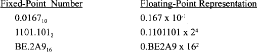
In converting from fixed-point to floating-point number representation, the resulting mantissas are normalized, that is, the digits of the fixed-point numbers are shifted so that the highest-order nonzero digit appears to the right of the decimal point and a 0 always appears to the left of the decimal point. This convention is normally adopted in floating-point number representation. Because all numbers will be assumed to be in normalized form, the binary point is not required to be represented in microprocessors.
Typical 32-bit microprocessors such as the Intel Pentium and the Motorola 68040 contain on-chip floating-point hardware. This means that these microprocessors can be programmed using instructions to perform operations such as addition, subtraction, multiplication, and division using floating-point numbers. The Motorola 68020 does not contain on-chip floating-point hardware but 68020 can be interfaced to a floating-point coprocessor chip to provide floating-point functions.
1.3 Evolution of the Microprocessor
The Intel Corporation is generally acknowledged as the company that introduced the first microprocessor successfully into the marketplace. Its first processor, the 4004, was introduced in 1971 and evolved from a development effort while making a calculator chip set. The 4004 microprocessor was the central component in the chip set, which was called the MCS-4. The other components in the set were a 4001 ROM, a 4002 RAM, and a 4003 shift register.
Shortly after the 4004 appeared in the commercial marketplace, three other general-purpose microprocessors were introduced: the Rockwell International 4-bit PPS-4, the Intel 8-bit 8008, and the National Semiconductor 16-bit IMP-16. Other companies, such as General Electric, RCA, and Viatron, also made contributions to the development of the microprocessor prior to 1971.
The microprocessors introduced between 1971 and 1972 were the first-generation systems designed using PMOS technology. In 1973, second-generation microprocessors such as the Motorola 6800 and the Intel 8080 (8-bit microprocessors) were introduced. The second-generation microprocessors were designed using NMOS technology. This technology resulted in a significant increase in instruction execution speed over PMOS and higher chip densities. Since then, microprocessors have been fabricated using a variety of technologies and designs. NMOS microprocessors such as the Intel 8085, the Zilog Z80, and the Motorola 6800/6809 were introduced based on second-generation microprocessors. A third generation HMOS microprocessor, introduced in 1978 is typically represented by the Intel 8086 and the Motorola 68000, which are 16-bit microprocessors.
During the 1980's, fourth-generation HCMOS and BICMOS (a combination of bipolar and HCMOS) 32-bit microprocessors evolved. Intel introduced the first commercial 32-bit microprocessor, the problematic Intel 432, which was eventually discontinued. Since 1985, more 32-bit microprocessors have been introduced. These include Motorola's 68020, 68030, 68040, 68060, PowerPC, Intel's 80386, 80486, the Intel Pentium family, Core Duo, and Core2 Duo microprocessors..
The performance offered by the 32-bit microprocessor is more comparable to that of superminicomputers such as Digital Equipment Corporation's VAX11/750 and VAX11/780. Intel and Motorola also introduced RISC microprocessors: the Intel 80960 and Motorola 88100/PowerPC, which had simplified instruction sets. Note that the purpose of RISC microprocessors is to maximize speed by reducing clock cycles per instruction. Almost all computations can be obtained from a simple instruction set. Note that, in order to enhance performance significantly, Intel Pentium Pro and other succeeding members of the Pentium family and Motorola 68060 are designed using a combination of RISC and CISC.
An overview of the Motorola 68XXX and PowerPC microprocessors will be provided next. Motorola's 32-bit microprocessors based on the 68000 (16-bit microprocessor) architecture include the MC68020, MC68030, MC68040, and MC68060. Table 1.1 compares the basic features of some of these microprocessors with the 68000.
MC68020 is Motorola's first 32-bit microprocessor. The design of the 68020 is based on the 68000. The 68020 can perform a normal read or write cycle in 3 clock cycles without wait states as compared to the 68000, which completes a read or write operation in 4 clock cycles without wait states. As far as the addressing modes are concerned, the 68020 includes new modes beyond those of the 68000. Some of these modes are scaled indexing, larger displacements, and memory indirection.
TABLE 1.1 Motorola 68000 vs. 68020/68030/68040
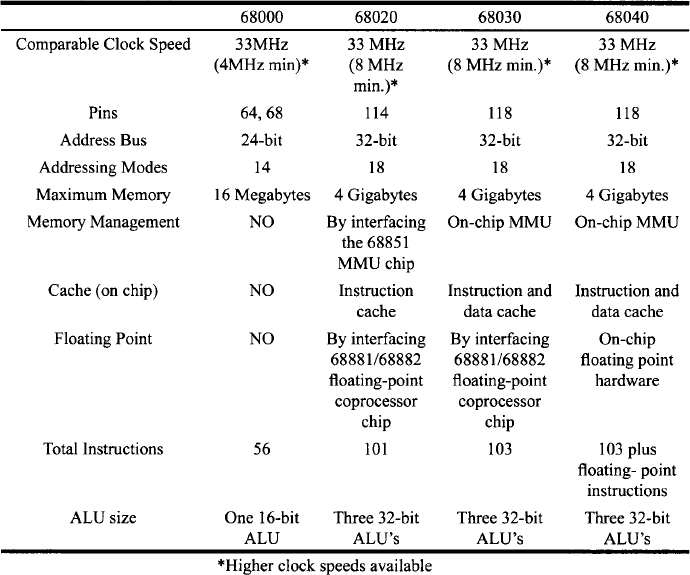
Furthermore, several new instructions are added to the 68020 instruction set, including the two new instructions are used to perform conversions between packed BCD and ASCII or EBCDIC digits. Note that a packed BCD is a byte containing two BCD digits.
68030 and 68040 are two enhanced versions of the 68020. The 68030 retains most of the 68020 features. It is a virtual memory microprocessor containing an on-chip MMU (memory management unit). The 68040 expands the 68030 on-chip memory management logic to two units: one for instruction fetch and one for data access. This speeds up the 68040's execution time by performing logical-to-physical-address translation in parallel. The on-chip floating-point capability of the 68040 provides it with both integer and floating-point arithmetic operations at a high speed. All 68000 programs written in assembly language in user mode will run on the 68020/68030 or 68040.
MC68060 is a superscalar (two instructions per cycle) 32-bit microprocessor. The 68060, like the Pentium Pro and the succeeding members of the Pentium family, is designed using a combination of RISC and CISC architectures to obtain high performance. For some reason, Motorola does not offer MC68050 microprocessor. The 68060 is fully compatible with the 68040 in the user mode. The 68060 can operate at 50- and 66-MHz clocks with performance much faster than the 68040. An striking feature of the 68060 is the power consumption control. The 68060 is designed using static HCMOS to reduce power during normal operation.
PowerPC family of microprocessors were jointly developed by Motorola, IBM, and Apple. The PowerPC family contains both 32- and 64-bit microprocessors. One of the noteworthy feature of the PowerPC is that it is the first top-of-the-line microprocessor to include an on-chip real-time clock (RTC). The RTC is common in single-chip microcomputers rather than microprocessors. The PowerPC is the first microprocessor to implement this on-chip feature, which makes it easier to satisfy the requirements of timekeeping for task switching and calendar date of modern multitasking operating systems. The PowerPC microprocessor supports both the Power Mac and standard PCs. The PowerPC family is designed using RISC architecture.
An overview of Intel's 80XXX, Pentium, and contemporary microprocessors will be provided in the following.
The original Pentium processor was introduced by Intel in 1993, and the name was changed from 80586 to Pentium because of copyright laws. The processor uses more than 3 million transistors and had an initial speed of 60 MHz. The speed has increased over the years to the latest speed of 233 MHz. Table 1.2 compares compares the basic features of the Intel 80386DX, 80386SX, 80486DX, 80486SX, 80486DX2, and Pentium. These are all 32-bit microprocessors. Note that the 80386SL (not listed in the table) is also a 32-bit microprocessor with a 16-but data bus like the 80386SX. The 80386SL can run at a speed of up to 25 MHz and has a direct addressing capability of 32 MB. The 80386SL provides virtual memory support along with on-chip memory management and protection. It can be interfaced to the 80387SX to provide floating-point support. The 80386SL includes an on-chip disk controller hardware.
The Pentium Pro was introduced in November 1995. The Pentium processor provides pipelined superscalar architecture. The Pentium processor's pipelined implementation uses five stages to extract high throughput and the Pentium Pro utilizes 12-stage, superpipelined implementation, trading less work per pipestage for more stages. The Pentium Pro processor reduced its pipe stage time by 33% compared with a Pentium processor, which means the Pentium Pro processor can have a 33% higher clock speed than a Pentium processor and still be equally easy to produce from a semiconductor manufacturing process. A 200-MHz Pentium Pro is always faster than a 200-MHz Pentium for 32-bit applications such as computer-aided design (CAD), 3-D graphics, and multimedia applications.
The Pentium processor's superscalar architecture, with its ability to execute two instructions per clock, was difficult to exceed without a new approach. The new approach used by the Pentium Pro processor removes the constraint of linear instruction sequencing between the traditional fetch and execute phases, and opens up a wide instruction pool. This approach allows the execute phase of the Pentium Pro processor to have much more visibility into the program's instruction stream so that better scheduling may take place. This allows instructions to be started in any order but always be completed in the original program order.
Microprocessor speeds have increased tremendously over the past several years, but the speed of the main memory devices has only increased by 60 percent. This increasing memory latency, relative to the microprocessor speed, is a fundamental problem that the Pentium Pro is designed to solve. The Pentium Pro processor looks ahead into its instruction pool at subsequent instructions and will do useful work rather than be stalled. The Pentium Pro executes instructions depending on their readiness to execute and not on their original program order. In summary, it is the unique combination of improved branch prediction, choosing the best order, and executing the instructions in the preferred order that enables the Pentium Pro processor to improve program execution over the Pentium processor. This unique combination is called dynamic execution.
TABLE 1.2 Intel 80386/80486/Pentium Microprocessors.

TABLE 1.3 Pentium vs. Pentium Pro.
| Pentium | Pentium Pro |
| • First introduced March 1993 | • Introduced November 1995 |
| • 2 instructions per clock cycle | • 3 instructions per clock cycle |
| • Primary cache of 16K | • Primary cache of 16K |
| • Original clock speeds of 100, 120, 133, 150, 166, 200, and 233 MHz | • Original clock speeds 166, 180, 200 MHz |
| • More silicon is needed to produce the chip | • Tighter design reduces silicon needed and makes chip faster (shorter distances between transistors) |
| • Designed for operating systems written in 16-bit code | • Designed for operating systems written in 32-bit code. |
The Pentium Pro does a great job running some operating systems such as Windows NT or Unix. The first release of Windows 95 contains a significant amount of 16-bit code in the graphics subsystem. This causes operations on the Pentium Pro to be serialized instead of taking advantage of the dynamic execution architecture. Nevertheless, the Pentium Pro is up to 30% faster than the fastest Pentium in 32-bit applications. Table 1.3 compares the basic features of the Pentium with the Pentium Pro.
The 32-bit Pentium II processor is Intel's next addition to the Pentium line of microprocessors, which originated form the widely cloned 80×86 line. It basically takes attributes of the Pentium Pro processor plus the capabilities of MMX technology to yield processor speeds of 333, 300, 266, and 233 MHz. The Pentium II processor uses 0.25 micron technology (this refers to the width of the circuit lines on the silicon) to allow increased core frequencies and reduce power consumption. The Pentium II processor took advantage of four technologies to achieve its performance ratings:
- Dual Independent Bus Architecture (DIB)
- Dynamic Execution
- Intel MMX Technology
- Single-Edge-Contact Cartridge
DIB was first implemented in the Pentium Pro processor to address bandwidth limitations. The DIB architecture consists of two independent buses, an L2 cache bus and a system bus, to offer three times the bandwidth performance of single bus architecture processors. The Pentium II processor can access data from both buses simultaneously to accelerate the flow of information within the system.
Dynamic execution was also first implemented in the Pentium Pro processor. It consists of three processing techniques to improve the efficiency of executing instructions. These techniques include multiple branch prediction, data flow analysis, and speculative execution. Multiple branch prediction uses an algorithm to determine the next instruction to be executed following a jump in the instruction flow. With data flow analysis, the processor determines the optimum sequence for processing a program after looking at software instructions to see if they are dependent on other instructions. Speculative execution increases the rate of execution by executing instructions ahead of the program counter that are likely to be needed.
MMX (matrix math extensions) technology is Intel's greatest enhancement to its microprocessor architecture. MMX technology is intended for efficient multimedia and communications operations. To achieve this, 57 new instructions have been added to manipulate and process video, audio, and graphical data more efficiently. These instructions support single-instruction multiple-data (SIMD) techniques, which enable one instruction to perform the same function on multiple pieces of data. Programs written using the new instructions significantly enhance the capabilities of Pentium II.
The final feature in Intel's Pentium II processor is single-edge-contact (SEC) packaging. In this packaging arrangement, the core and L2 cache are fully enclosed in a plastic and metal cartridge. The components are surface mounted directly to a substrate inside the cartridge to enable high-frequency operation.
Intel Celeron processor utilizes Pentium II as core. The Celeron processor family includes: 333 MHz, 300A MHz, 300 MHz, and 266 MHz processors. The Celeron 266 MHz and 300 MHz processors do not contain any level 2 cache. But the Celeron 300A MHz and 333 MHz processors incorporate an integrated L2 cache. All Celeron processors are based on Intel's 0.25 micron CMOS technology. The Celeron processor is designed for inexpensive or “Basic PC” desktop systems and can run Windows 98. The Celeron processor offers good floating-point (3D geometry calculations) and multimedia (both video and audio) performance.
The Pentium II Xeon processor contains large, fast caches to transfer data at super high speed through the processor core. The processor can run at either 400 MHz or 450 MHz. The Pentium II Xeon is designed for any mid-range or higher Intel-based server or workstation. The 450 MHz Pentium II Xeon can be used in workstations and servers.
The Pentium III operates at 450 MHz and 500 MHz. It is designed for desktop PCs. The Pentium III enhances the multimedia capabilities of the PC, including full screen video and graphics. Pentium III Xeon processors run at 500 MHz and 550 MHz. They are designed for mid-range and higher Internet-based servers and workstations. It is compatible with Pentium II Xeon processor-based platforms. Pentium III Xeon is also designed for demanding workstation applications such as 3-D visualization, digital content creation, and dynamic Internet content development. Pentium Ill-based systems can run applications on Microsoft Windows NT or UNIX-based environments. The Pentium III Xeon is available in a number of L2 cache versions such as 512-Kbytes, 1-Mbyte, or 2-Mbytes (500 MHz); 512 Kbytes (550 MHz) to satisfy a variety of Internet application requirements.
The Intel Pentium 4 is an enhanced Pentium III processor. It is currently available at 1.30, 1.40, 1.50, and 1.70 GHz. The chip's all-new internal design contains Intel NetBurstTM micro-architecture. This provides the Pentium 4 with hyper pipelined technology ( which doubles the pipeline depth to 20 stages), a rapid execution engine ( which pushes the processor's ALUs to twice the core frequency), and 400 MHz system bus. The Pentium 4 contains 144 new instructions. Furthermore, inclusion of an improved Advanced Dynamic Execution and an improved floating point pushes data efficiently through the pipeline. This enhances digital audio, digital video and 3D graphics. Along with other features such as streaming SIMD Extensions 2 (SSE2) that extends MMXTM technology, the Pentium 4 gives the advanced technology to get the most out of the Internet. Finally, the Pentium 4 offers high performance when networking multiple PCs, or when attaching Pentium 4 based PC to home consumer electronic systems and new peripherals.
Intel introduced the 32-bit Pentium M microprocessor in 2003. It was designed specifically for the mobile computing market. The Pentium M contains approximately 77 million transistors and originally ran at a speed of 1.3 to 1.6 GHz. In 2006, Intel introduced the 64-bit Core Duo microprocessor. The Core Duo is based on the Pentium M microarchitecture. The Core Duo contains approximately 151 million transistors. The original Core Duo ran at a speed of 1.66 to 2.33 GHz. The Core Duo is used primarily in servers.
Intel introduced the Core 2 Duo microprocessor in 2006, based on Core Duo microarchitecture. The Core 2 Duo contains approximately 291 million transistors and is used in desktop computers. The original Core 2 Duo ran at a speed of 1.86 to 2.93 GHz.
Note that Intel 4004 contained approximately 2300 transistors with a clock frequency of about 100 kHz. In contrast, contemporary microprocessors such as Intel Core Duo contain over 100 million transistors with a frequency of more than 2 GHz. These microprocessors are typically used in designing client and server systems for the Internet.
An overview of the latest microprocessors is provided in this section. Unfortunately, this may be old news within a few years. One can see, however, that both Intel and Motorola offer (and will continue to offer) high-quality microprocessors to satisfy demanding applications.
1.4 Typical Features of 32-bit and 64-bit Microprocessors
In this section we describe the basic aspects of typical 32- and 64-bit microprocessors. Topics include on-chip features such as pipelining, memory management, floating-point, and cache memory implemented in typical 32- and 64-bit microprocessors. The first 32-bit microprocessor, Intel's problematic iAPX432, was introduced in 1980. Soon afterward, the concept of mainframe on a chip or micromainframe was used to indicate the capabilities of these microprocessors and to distinguish them from previous 8- and 16-bit microprocessors.
The introduction of several 32-bit microprocessors revolutionized the microprocessor world. The performance of these 32-bit microprocessors is actually more comparable to that of superminicomputers such as Digital Equipment Corporation's VAX11/750 and VAX11/780. Designers of 32-bit microprocessors have implemented many powerful features of these mainframe computers to increase the capabilities of microprocessor chip sets: pipelining, on-chip cache memory, memory management, and floating-point arithmetic.
In pipelining, instruction fetch and execute cycles overlap. This method allows simultaneous preparation for execution of one or more instructions while another instruction is being executed. Pipelining was used for many years in mainframe and minicomputer CPUs to speed up the instruction execution time of these machines. The 32-bit microprocessors implement the pipelining concept and operate simultaneously on several 32-bit words, which may represent different instructions or part of a single instruction.
Although pipelining greatly increases the rate of execution of nonbranching code, pipelines must be emptied and refilled each time a branch or jump instruction appears in the code. This may slow down the processing rate for code with many branches or jumps. Thus, there is an optimum pipeline depth, which is strongly related to the instruction set, architecture, and gate density attainable on the processor chip.
With memory management, virtual memory techniques, traditionally a feature of mainframes, are also implemented as on-chip hardware on typical 32-bit microprocessors. This allows programmers to write programs much larger than those that could fit in the main memory space available to microprocessors; the programs are simply stored on a secondary device such as a hard disk, and portions of the program are swapped into main memory as needed.
Segmentation circuitry has been included in many 32-bit microprocessor chips. With this technique, blocks of code called segments, which correspond to modules of the program and have varying sizes set by the programmer or compiler, are swapped. For many applications, however, an alternative method borrowed from mainframes and superminis called paging is used. Basically, paging differs from segmentation in that pages are of equal size. Demand paging, in which the operating system swaps pages automatically as needed, can be used with all 32-bit microprocessors.
Floating-point arithmetic is yet another area in which the new chips mimick mainframes. With early microprocessors, floating-point arithmetic was implemented in software largely as a subroutine. When required, execution would jump to a piece of code that would handle the tasks. This method slows the execution rate considerably, however, so floating-point hardware such as fast bit-slice (registers and ALU on a chip) processors and, in some cases, special-purpose chips was developed. Other than the Intel 8087, these chips behaved more or less like peripherals. When floating-point arithmetic was required, the problems were sent to the floating-point processor and the CPU was freed to move on to other instructions while it waited for the results. The floating-point processor is implemented as on-chip hardware in typical 32-bit microprocessors, as in mainframe and minicomputer CPUs. Caching or memory-management schemes are utilized with all 32-bit microprocessors to minimize access time for most instructions.
A cache, used for years in minis and mainframes, is a relatively small, high-speed memory installed between a processor and its main memory. The theory behind a cache is that a significant portion of the CPU time spent running typical programs is tied up in executing loops; thus, chances are good that if an instruction to be executed is not the next sequential instruction, it will be one of some relatively small number of instructions clustering around a small region in the main memory, a concept known as locality of reference. Therefore, a high-speed memory large enough to contain most loops should greatly increase processing rates. Cache memory is included as on-chip hardware in typical 32-bit microprocessors such as the Pentium.
Typical 32-bit microprocessors such as Pentium and PowerPC chips are superscalar processors. This means that they can execute more than one instruction in one clock cycle. Also, some 32-bit microprocessors such as the PowerPC contain an on-chip real-time clock. This allows these processors to use modern multitasking operating systems that require timekeeping for task switching and for keeping the calendar date.
Typical 32-bit microprocessors implement a multiple-branch prediction feature. This allows these microprocessors to anticipate jumps of the instruction flow. Also, some 32-bit microprocessors determine an optimal sequence of instruction execution by looking at decoded instructions and determining whether to execute or hold them. Typical 32bit microprocessors use a “look-ahead” approach to execute instructions. These 32-bit microprocessors maintain an instruction pool for a sequence of instructions and perform a useful task rather than executing the present instruction and going on to the next.
The 64-bit microprocessors such as Power PC 750 include all the features of 32-bit microprocessors. In addition, they contain multiple on-chip integer and floating-point units and a larger address and data buses. The 64-bit microprocessors can typically execute four instructions per clock cycle and can run at a clock speed of over 2 GHz. The original Pentium microprocessor is a CISC microprocessor. Pentium Pro and other succeeding members of the Pentium family are designed using a combination of mostly microprogramming (CISC) and some hardwired control (RISC) whereas the PowerPC is designed using hardwired control with almost no microcode. The PowerPC is a RISC microprocessorand therefore includes a simple instruction set. This instruction set includes register-to-register, load, and store instructions. All instructions involving arithmetic operations use registers; load and store instructions are utilized to access memory. Almost all computations can be obtained from these simple instructions. Finally, 64-bit microprocessors are ideal candidates for data-crunching machines and high-performance desktop systems and workstations.
1.5 Microprocessor-based System Design Concepts
A microprocessor-based system is typically designed using a microcomputer development system a tool that allows the designer to develop, debug, and integrate error-free application software in microprocessor systems. Development systems fall into one of two categories: systems supplied by the device manufacturer (nonuniversal systems) and systems built by after-market manufacturers (universal systems). The main difference between the two categories is in the range of microprocessors that a system will accommodate. Nonuniversal systems are supplied by the microprocessor manufacturer (e.g., Intel, Motorola) and are limited to use for the particular microprocessor manufactured by the supplier. In this manner, an Intel development system may not be used to develop a Motorola-based system. Universal development systems (e.g., Hewlett-Packard) can develop hardware and software for several microprocessors.
Within both categories of development systems, basically two types are available: single-user and networked systems. A single-user system consists of one development station that can be used by one user at a time. Single-user systems are low in cost and may be sufficient for small systems development. A networked system usually consists of a number of smart terminals capable of performing most development work and can be connected over data lines to a central microcomputer. The central microcomputer in a networked system usually is in charge of allocating disk storage space and will download some programs into the user's workstation microcomputer. A microcomputer development system is a combination of the hardware necessary for microprocessor design and software to control the hardware. The basic components of the hardware are a central processor, a terminal, a mass storage device (e.g., hard disk), and usually an in-circuit emulator (ICE).
In a single-user system, the central processor executes the operating system software, handles the input/output (I/O) facilities, executes the development programs (e.g., editor, assembler, linker), and allocates storage space for the programs being executed. In a large multiuser networked system the central processor may be responsible for the I/O facilities and execution of development programs. The terminal provides the interface between the user and the operating system or program under execution. The user enters commands or data via the keyboard, and the program under execution displays data to the user on the screen. Each program (whether system software or user program) is stored in an ordered format on disk. Each separate entry on the disk is called a file. The operating system software contains the routines necessary to interface between the user and the mass storage unit. When the user requests a file by a specific file name, the operating system finds the program stored on disk by the file name and loads it into main memory. Typical development systems contain memory management software that protects a user's files from unauthorized modification by another user. This is accomplished by means of a unique user identification code called userid. A user can only access files that have the user's unique code. The equipment listed here makes up a basic development system, but most systems have other devices, such as printers and EPROM programmers, attached. A printer is needed to provide the user with a hard copy record of the program under development.
After the application software has been developed and debugged completely, it needs to be stored permanently in the target hardware. The EPROM (erasable/programmable read-only memory) programmer takes the machine code and programs it into an EPROM. EPROMs are still widely used in typical system development..
Most development systems support one or more in-circuit emulators (ICEs). An ICE is a very useful tool for microprocessor hardware development. To use an ICE, the microprocessor chip is removed from the system under development (called the target processor) and the emulator is plugged into the microprocessor socket. Functionally and electrically, the ICE will act identically to the target processor with the exception that the ICE is under the control of development system software. In this manner the development system may exercise the hardware that is being designed and monitor all status information available about the operation of the target processor. Using an ICE, the processor register contents may be displayed on the screen and operation of the hardware observed in a single-stepping mode. In-circuit emulators can find hardware and software bugs quickly that might take many hours to locate using conventional hardware testing methods.
Typical programs provided for microprocessor development are the operating system, editor, assembler, linker, compiler, and debugger. The operating system is responsible for executing the user's commands. The operating system handles I/O functions, memory management, and loading of programs from mass storage into RAM for execution. The editor allows the user to enter the source code (either assembly language or some high-level language) into the development system.
Typical microprocessor development systems use a character-oriented editor, more commonly referred to as a screen editor, so called because the text is dynamically displayed on the screen and the display updates automatically any edits made by the user. The screen editor uses the pointer concept to point to characters that need editing. The pointer in a screen editor is called the cursor, and special commands allow the user to position the cursor at any location displayed on the screen. When the cursor is positioned, the user may insert characters, delete characters, or simply type over the existing characters.
Complete lines may be added or deleted using special editor commands. By placing the editor in the insert mode, any text typed will be inserted at the cursor position when the cursor is positioned between two existing lines. If the cursor is positioned on a line to be deleted, a single command will remove the entire line from the file. Screen editors implement the editor commands in different fashions. Some editors use dedicated keys to provide some cursor movements. The cursor keys are usually marked with arrows to show the direction of cursor movement. Some popular editors (such as the Hewlett-Packard HP 64XXX) use soft keys which are unmarked keys located on the keyboard directly below the bottom of the CRT screen. The mode of the editor decides what functions the keys are to perform. The function of each key is displayed on the screen directly above the appropriate key. The soft key approach is valuable because it allows the editor to reassign a key to a new function when necessary.
The source code generated on the editor is stored as ASCII or text characters and cannot be executed by a microprocessor. Before the code can be executed, it must be converted to a form accessible by the microprocessor. An assembler is the program used to translate the assembly language source code generated with an editor into object code (machine code), that can be executed by a microprocessor.
The output file from most development system assemblers is an object file usually a relocatable code that may be configured to execute at any address. The function of the linker is to convert the object file to an absolute file, which consists of the actual machine code at the correct address for execution. Absolute files thus created are used for debugging and for programming EPROMs.
Debugging a microprocessor-based system may be divided into two categories: software debugging and hardware debugging. Each debugging process is usually carried out separately because software debugging can be carried out on an out-of-circuit emulator without having the final system hardware. The usual software development tools provided with the development system are a single stepper and a breakpoint.
A single stepper simply allows the user to execute the program being debugged one instruction at a time. By examining the register and memory contents during each step, the debugger can detect such program faults as incorrect jumps, incorrect addressing, erroneous op-codes, and so on. A breakpoint allows the user to execute an entire section of a program being debugged. There are two types of breakpoints: hardware and software. A hardware breakpoint uses the hardware to monitor the system address bus and detect when the program is executing the desired breakpoint location. When the breakpoint is detected, the hardware uses the processor control lines to halt the processor for inspection or cause the processor to execute an interrupt to a breakpoint routine. Hardware breakpoints can be used to debug both ROM- and RAM-based programs. Software breakpoint routines may only operate on a system with the program in RAM because the breakpoint instruction must be inserted into the program that is to be executed.
Single-stepper and breakpoint methods complement each other. The user may insert a breakoint at the desired point and let the program execute up to that point. When the program stops at the breakpoint, the user may use a single-stepper to examine the program one instruction at a time. Thus, the user can pinpoint the error in a program.
There are two main hardware-debugging tools: the logic analyzer and the in-circuit emulator. Logic analyzers are commonly used to debug hardware faults in a system. The logic analyzer is the digital version of an oscilloscope because it allows the user to view logic levels in the hardware. In-circuit emulators can be used to debug and integrate software and hardware. Inexpensive PC-based workstations are used extensively as development systems.
The total development of a microprocessor-based system typically involves three phases: software design, hardware design, and program diagnostic design. A systems programmer will be assigned the task of writing the application software, a logic designer will be assigned the task of designing the hardware, and typically, both designers will be assigned the task of developing diagnostics to test the system. For small systems, one engineer may do all three phases, and on large systems several engineers may be assigned to each phase. Figure 1.1 shows a flowchart for the total development of a system. Notice that software and hardware development may occur in parallel to save time.
The first step in developing the software is to take the system specifications and write a flowchart to accomplish the tasks that will implement the specifications. The assembly language or high-level source code may now be written from the system flowchart. The complete source code is then assembled. The assembler is the object code and a program listing. The object code will be used later by the linker. The program listing may be sent to a disk file for use in debugging, or it may be directed to the printer.
The linker can now take the object code generated by the assembler and create the final absolute code that will be executed on the target system. The emulation phase will take the absolute code and load it into the development system RAM. From here, the program may be debugged using breakpoints or single stepping.
Working from the system specifications, a block diagram of the hardware must be developed. The logic diagram and schematics may now be drawn using the block diagram as a guide, and a prototype may now be constructed and tested for wiring errors. When the prototype has been constructed, it may be debugged for correct operation using standard electronic testing equipment such as oscilloscopes, meters, logic probes, and logic analyzers, all with test programs created for this purpose. After the prototype has been debugged electrically, the development system in-circuit emulator may be used to check it functionally. The ICE will verify the memory map, correct I/O operation, and so on. The next step in system development is to validate the complete system by running operational checks on the prototype with the finalized application software installed. The EPROMs are then programmed with the error-free programs.
1.6 Typical Microprocessor Applications
Microprocessors are extensively used in a wide variety of applications. A simple microprocessor application along with some typical applications are briefly described in the following.
1.6.1 A Simple Microprocessor Application
To put microprocessors into perspective, it is important to explore a simple application. For example, consider the microprocessor-based dedicated controller shown in Figure 1.2. Suppose that it is necessary to maintain the temperature of a furnace to a desired level to maintain the quality of a product. Assume that the designer has decided to control this temperature by adjusting the fuel. This can be accomplished using a microcomputer along with the interfacing components as follows. Temperature is an analog (continuous) signal. It can be measured by a temperature-sensing (measuring) device such as a thermocouple. The thermocouple provides the measurement in millivolts (mV) equivalent to the temperature. Since microcomputers only understand binary numbers (0's and 1's), each analog mV signal must be converted to a binary number using an analog-to-digital (A/D) converter chip.

FIGURE 1.1 Microprocessor system development flowchart
First, the millivolt signal is amplified by a mV/V amplifier to make the signal compatible for A/D conversion. A microcomputer can be programmed to solve an equation with the furnace temperature as an input. This equation compares the temperature measured with the temperature desired which can be entered into the microcomputer using the keyboard. The output of this equation will provide the appropriate opening and closing of the fuel valve to maintain the appropriate temperature. Since this output is computed by the microcomputer, it is a binary number. This binary output must be converted into an analog current or voltage signal.
The D/A (digital-to-analog) converter chip inputs this binary number and converts it into an analog current (I). This signal is then input into the current/pneumatic (I/P) transducer for opening or closing the fuel input valve by air pressure to adjust the fuel to the furnace. The furnace temperature desired can thus be achieved. Note that a transducer converts one form of energy (analog electrical current in this case) to another form (air pressure in this example).
1.6.2 Examples of Typical Microprocessor Applications
Microprocessors are used in designing personal workstations. These workstations can provide certain sophisticated functions such as IC layout, 3D graphics, and stress analysis.
In many applications such as control of life-critical systems, control of nuclear waste, and unattended remote system operation, the reliability of the hardware is of utmost importance. The need for such reliable systems resulted in fault-tolerant systems. These systems use redundant microprocessors to provide reliable operation.
Real-time controllers such as flight-control systems for aircraft, flight simulators, and automobile engine control require high-performance microprocessors. For example, the flight simulators use multiple microprocessors to perform graphic manipulation, data gathering, and high-speed communications.
Microprocessors are widely used in robot control systems. In many cases, the microprocessor is used as the brain of the robot. In a typical application, the microprocessor will input the actual arm angle measurement from a sensor, compare it with the desired arm angle, and will then send outputs to a motor to position the arm. Mitsubishi manufactured the first 68020-based robot control system.

FIGURE 1.2 Furnace Temperature Control
Implementation of the on-chip floating-point unit (FPU) in 32-bit microprocessors such as the Pentium and 68040 makes it appropriate for wide areas of numeric applications:
- Typical FPU's can accept decimal operands and produce extra decimal results of up to several digits. This greatly simplifies accounting programming. Financial calculations that use power functions can take advantage of exponential and logarithmic functions.
- Many minicomputer and mainframe large simulation problems can be executed by the 32-bit microprocessors. These applications include complex electronic circuit simulations using SPICE and simulation of mechanical systems using finite element analysis.
- The FPU's implemented in typical 32-bit microprocessors can move and position machine control heads with accuracy in real time. Axis positioning can efficiently be performed by the hardware trigonometric support provided by the FPU. The 32-bit microprocessors can, therefore, be used for computer numerical control (CNC) machines. CNC machines are extensively used in manufacturing intraocular (cataract implant) lenses.
- The pipelined instruction feature of the 32-bit microprocessor makes it an ideal candidate for DSP (digital signal processing) and related applications for computing matrix multiplications and convolutions.
Embedded Control microprocessors, also called embedded controllers, are designed to manage specific tasks. Once programmed, the embedded controllers can manage the functions of a wide variety of electronic products. Since the microprocessors are embedded in the host system, their presence and operation are basically hidden from the host system. Typical embedded control applications include office automation products such as copiers, laser products, fax machines, and consumer electronics such as VCRs, microwave ovens. Applications such as laser printers require a high performance microprocessor with on-chip floating-point hardware. The RISC microprocessors are ideal for these types of applications. Note that the PC interfaced to the laser printer is the host.
RISC microprocessors such as the PowerPC are well suited for applications such as image processing, robotics, graphics, and instrumentation. The key features of the RISC microprocessors that make them ideal for these applications are their relatively low level of integration in the chip, and instruction pipeline architecture. These characteristics result in low power consumption, fast instruction execution, and fast recognition of interrupts.
Also, note that the Power PC contains an on-chip Real Time Clock (RTC). In the past, the on-chip RTC was common to single chip microcomputers, Power PC is the first top of the line microprocessor to implement the on-chip RTC. This facilitates implementation of multitasking operating systems which require time keeping for task switching as well as keeping the calendar date.