9
68020 HARDWARE AND INTERFACING
In this chapter we describe the fundamental concepts associated with hardware aspects of the Motorola 68020 microprocessor. Significant modifications have been made to the 68020 bus structure beyond those of the 68000. One of these enhancements is dynamic bus sizing. Hence, this feature along with 68020 system design concepts are included. Topics covered in this chapter include 68020 pins and signals, dynamic bus sizing, and system design concepts. Finally, design concepts associated with a 68020-based voltmeter and a 68020-based microcomputer interface to a hexadecimal keyboard and a seven-segment display are covered. These topics are described in a simplified manner. Note that a background in the 68000 software and hardware described in Chapters 6 and 7 is required to understand the topics contained in this chapter.
9.1 Introduction
In this section we describe hardware aspects of the 68020. Topics include 68020 pins and signals, aligned and misaligned transfers, dynamic bus sizing, and timing diagrams. Numerous changes have been made to the 68020 bus structure. Note that the 68020 does not support 6800-type I/O devices. As mentioned in Chapter 7, the 68000 supports both 6800-type I/O devices such as 6821 and 16-bit devices such as 68230. Also, the 68020 can complete read or write bus cycles in three clock cycles without wait states. This is due to enhancements made in the 68020 bus control logic. The 68000, on the other hand, requires four cycles to complete read or write cycles without wait states.
9.1.1 68020 Pins and Signals
The 68020 is arranged in a 13 × 13 matrix array (114 pins defined) and fabricated in a pin grid array (PGA) or other packages, such as an RC suffix package. Both the 32-bit address (A0–A31) and data (D0–D31) pins of the 68020 are nonmultiplexed. The 68020 transfers data with an 8-bit device via D31–D24, with a 16-bit device via D31–D16, and with a 32-bit device via D31–D0. Figure 9.1 shows the 68020 functional signal group. For reliable operation, unused inputs should be connected to an appropriate signal level. Unused active LOW inputs should be connected to Vcc. Unused active HIGH inputs should be connected to GROUND.
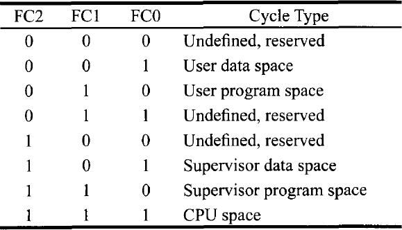
Table 9.1 lists these signals along with a description of each. Ten Vcc (+5 V) and 13 ground pins are used to distribute power in order to reduce noise. As stated above, unused inputs should not be kept floating. Unused active LOW inputs should be connected to Vcc. Unused active HIGH inputs should be connected to GROUND. Like the 68000, the three function code signals FC2, FC1, and FC0 identify the processor state (supervisor or user) and the address space of the bus cycle currently being executed except that the 68020 defines the CPU space cycle as shown in Table 9.2. Note that in the 68000, FC2, FC1, FC0 =111 indicates the interrupt acknowledge cycle. In the 68020, it indicates the CPU space cycle. In this cycle, by decoding address lines A19–A16, the 68020 can perform various types of functions, such as coprocessor communication, breakpoint acknowledge, interrupt acknowledge, and module operations, as depicted in Table 9.3.
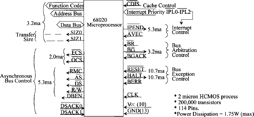
FIGURE 9.1 68020 functional signal groups.
TABLE 9.1 Hardware Signal Index

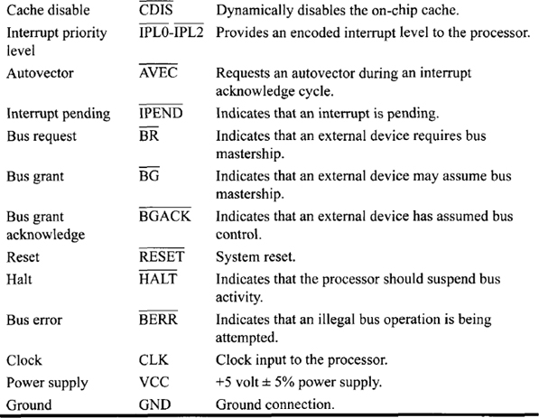
TABLE 9.2 68020 Function Code Signals
Note that A19, A18, A17, A16 = 00112 to 11102 is reserved by Motorola. In the coprocessor communication CPU space cycle, the 68020 determines the coprocessor type by decoding A15–A13 as shown in Table 9.4.
TABLE 9.3 Decoding of A19–A16 Pins During a CPU Space Cycle
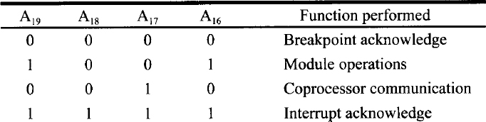
TABLE 9.4 Coprocessor Communication During a CPU Space Cycle

Let us explain some of the other 68020 pins. The ![]() (external cycle start) pin is a 68020 output pin. The 68020 asserts this pin during the first one-half clock of every bus cycle to provide the earliest indication of the start of a bus cycle. The use of
(external cycle start) pin is a 68020 output pin. The 68020 asserts this pin during the first one-half clock of every bus cycle to provide the earliest indication of the start of a bus cycle. The use of ![]() must be validated later with
must be validated later with ![]() , because the 68020 may start an instruction fetch cycle and then abort it if the instruction is found in the cache. In the case of a cache hit, the 68020 does not assert
, because the 68020 may start an instruction fetch cycle and then abort it if the instruction is found in the cache. In the case of a cache hit, the 68020 does not assert ![]() , but provides A3–A0, SIZ1, SIZ0, and FC2–FC0 outputs.
, but provides A3–A0, SIZ1, SIZ0, and FC2–FC0 outputs.
The 68020 ![]() input is activated by an external device to service an autovector interrupt. The
input is activated by an external device to service an autovector interrupt. The ![]() on the 68020 provides the same function as the
on the 68020 provides the same function as the ![]() on the 68000 during autovector interrupt. The functions of other signals, such as
on the 68000 during autovector interrupt. The functions of other signals, such as ![]() ,
, ![]() ,
, ![]() ,
, ![]() ,
, ![]() , and
, and ![]() , are similar to those of the 68000.
, are similar to those of the 68000.
The 68020 system control pins are functionally similar to those of the 68000. However, there are some minor differences. For example, for hardware reset, the ![]() and
and ![]() pins need not be asserted simultaneously. Therefore, unlike the 68000, the
pins need not be asserted simultaneously. Therefore, unlike the 68000, the ![]() and
and ![]() pins are not required to be tied together in the 68020 system .
pins are not required to be tied together in the 68020 system .
The ![]() and
and ![]() pins are bidirectional and open drain (external pull-up resistances are required), and their functions are independent. When asserted by an external circuit for a minimum of 520 clock periods, the
pins are bidirectional and open drain (external pull-up resistances are required), and their functions are independent. When asserted by an external circuit for a minimum of 520 clock periods, the ![]() pin resets the entire system, including the 68020. Upon hardware reset, the 68020 completes any active bus cycle in an orderly manner and then performs the following:
pin resets the entire system, including the 68020. Upon hardware reset, the 68020 completes any active bus cycle in an orderly manner and then performs the following:
- Reads the 32-bit content of address $00000000 and loads it into the ISP (the contents of $00000000 are loaded to the most significant byte of the ISP, and so on).
- Reads the 32-bit contents of address $00000004 into the PC (contents of $00000004 to the most significant byte of the PC, and so on).
- Sets the 12 11 10 bits of the SR to 1 1 1, sets the S bit in the SR to 1, and clears the T1, T0, and M bits in the SR.
- Clears the VBR to $00000000.
- Clears the cache enable bit in the CACR.
- No other registers are affected by hardware reset.
When the RESET instruction is executed, the 68020 asserts the ![]() pin LOW for 512 clock cycles, and the processor resets all the external devices connected to the
pin LOW for 512 clock cycles, and the processor resets all the external devices connected to the ![]() pin. Software reset does not affect any internal register.
pin. Software reset does not affect any internal register.
TABLE 9.5 Decoding of SIZ0 and SIZ1 Pins

TABLE 9.6 Device Size Definition by ![]() and
and ![]() Pins
Pins

In asynchronous operation, the 68020 typically uses bus signals such as ![]() ,
, ![]() ,
, ![]() , and
, and ![]() to control data transfer. Using asynchronous operation,
to control data transfer. Using asynchronous operation, ![]() starts the bus cycle and
starts the bus cycle and ![]() is used as a condition of valid data on a write cycle. Decoding SIZ1, SIZ0, A1, and A0 provides enable signals, which indicate the portion of the data bus that is used in data transfer. The memory or I/O chip then responds by placing the requested data on the correct portion of the data bus for a read cycle or latching the data on a write cycle and asserting
is used as a condition of valid data on a write cycle. Decoding SIZ1, SIZ0, A1, and A0 provides enable signals, which indicate the portion of the data bus that is used in data transfer. The memory or I/O chip then responds by placing the requested data on the correct portion of the data bus for a read cycle or latching the data on a write cycle and asserting ![]() and
and ![]() , corresponding to the memory or I/O port size (8-, 16-, or 32-bit), to terminate the bus cycle.
, corresponding to the memory or I/O port size (8-, 16-, or 32-bit), to terminate the bus cycle.
SIZ0 and SIZ1 pins indicate the number of bytes remaining to be transferred for a cycle; these signals, together with A0 and A1, define the active sections of the data bus. The decoding of SIZ0 and SIZ1 and the ![]() and
and ![]() pins are shown in Tables 9.5 and 9.6, respectively.
pins are shown in Tables 9.5 and 9.6, respectively.
EXAMPLE 9.1 Determine the contents of PC, SR, MSP, and ISP after a 68020 hardware reset. Assume a 32-bit memory with the following data prior to the reset: [$00000000] = $50001234, [$00000004] = $72152614, [MSP] = $27140124, [ISP] = $61711420, [PC] = $35261271, and [SR] = $0301.
Solution
After hardware reset, the following are the memory and register contents: [$00000000] = $50001234, [$00000004] = $72152614, [MSP] = $27140124, [ISP] = $50001234, [PC] = $72152614, and [SR] = $2701. Note that [SR] = $2701 = 00100111000000012. Compared with Figure 8.2, T1T0 = 00, S = 1, M = 0, and 12, 11, 10 = 111; other bits are not affected.
9.1.2 68020 Dynamic Bus Sizing
The 68020 offers a feature called dynamic bus sizing, which enables designers to use 8-, 16-, and 32-bit memory and I/O devices without sacrificing system performance. The SIZ0, SIZ1, ![]() , and
, and ![]() pins are used to implement the 68020 dynamic bus sizing. During each bus cycle, the external device indicates its width via
pins are used to implement the 68020 dynamic bus sizing. During each bus cycle, the external device indicates its width via ![]() and
and ![]() . The
. The ![]() and
and ![]() pins are used to indicate completion of the cycle. At the start of a bus cycle, the 68020 always transfers data to lines D0–D31, taking into consideration that the memory or I/O device may be 8, 16, or 32 bits wide. After the first bus cycle, the 68020 knows the device size by checking the
pins are used to indicate completion of the cycle. At the start of a bus cycle, the 68020 always transfers data to lines D0–D31, taking into consideration that the memory or I/O device may be 8, 16, or 32 bits wide. After the first bus cycle, the 68020 knows the device size by checking the ![]() and
and ![]() pins and generates additional bus cycles if needed to complete the transfer.
pins and generates additional bus cycles if needed to complete the transfer.

FIGURE 9.2 68020 dynamic bus sizing block diagram.
Next, consider an example of dynamic bus sizing. The 4 bytes of a 32-bit data can be defined as follows:

If this data is held in a data register Dn and is to be written to a memory or I/O location, the address lines A1 and A0 define the byte position of data. For a 32-bit device, A1A0 = 00 (addresses 0, 4, 8,…), A1A0 = 01 (addresses 1, 5, 9,…), A1A0= 10 (addresses 2, 6, 10,…), and A1A0 = 11 (addresses 3, 7, 11, …) will store OP0, OP1, OP2, and OP3, respectively. This data is written via the 68020 D31–D0 pins. However, if the device is 16-bit, data is always transferred as follows:
- All even-addressed bytes via pins D31–D24
- All odd-addressed bytes via pins D23–D16
Finally, for an 8-bit device, both even- and odd-addressed bytes are transferred via pins D31–D24. The 68020 always starts transferring data with the most significant byte first.
Figure 9.2 is a functional block diagram for 68020 interfaces to 8-, 16-, and 32-bit memory and I/O devices. Note that 8-bit devices perform data transfer with the 68020 via D31–D24 pins, 16-bit devices via D31–D16, and 32-bit devices via D31–D0 pins. Aligned long word transfers to 8-, 16-, and 32-bit devices are shown in Figure 9.3. For a 32-bit device, an address starting with A1A0 = 00 indicates a long word aligned transfer. The 68020 instruction, MOVE.L Dl,$50001234 is an example of an aligned long word transfer since A1A0 = 00. 68020 byte addressing is summarized in Figure 9.4. Figure 9.4 shows how four bytes of a 32-bit longword are transferred between the 68020 and a 32-bit device, 16-bit device, or an 8-bit device.
Figure 9.5 shows misaligned long word transfers to 8-, 16-, and 32-bit devices. The 68020 instruction MOVE.L D1,$50001235 is an example of a misaligned long word transfer since A1A0 = 01.
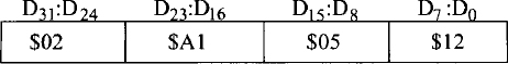
As an example of dynamic bus sizing, consider MOVE.L D1,$20107420. This is a long word aligned transfer. In the first bus cycle, the 68020 does not know the size of the device and hence outputs all combinations of data on pins D31–D0, taking into consideration that the device may be 8, 16, or 32 bits wide. Assume that the content of D1 is $02A10512 (OP0 = $02, OP1 = $A1, OP2 = $05, and OP3 = $12). In the first bus cycle, the 68020 sends SIZ1 SIZ0 = 00, indicating a 32-bit transfer, and then outputs data on its D31–D0 pins as follows:
If the device is 8-bit, it will take data $02 from pins D31–D24 in the first cycle and will then assert ![]() and
and ![]() as 10, indicating an 8-bit device. The 68020 then transfers the remaining 24 bits ($A1 first, $05 next, and $12 last) via pins D31–D24 in three consecutive cycles, with a total of four cycles being necessary to complete the transfer.
as 10, indicating an 8-bit device. The 68020 then transfers the remaining 24 bits ($A1 first, $05 next, and $12 last) via pins D31–D24 in three consecutive cycles, with a total of four cycles being necessary to complete the transfer.
However, if the device is 16-bit, in the first cycle the device will take the 16-bit data $02 A1 via pins D31–D16 and will then assert ![]() and
and ![]() as 01, indicating a 16-bit device. The 68020 then transfers the remaining 16 bits ($0512) via pins D31–D16 in the next cycle, requiring a total of two cycles for the transfer.
as 01, indicating a 16-bit device. The 68020 then transfers the remaining 16 bits ($0512) via pins D31–D16 in the next cycle, requiring a total of two cycles for the transfer.

FIGURE 9.3 Aligned long word transfer.
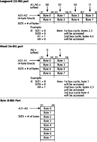
FIGURE 9.4 MC68020 byte addressing.
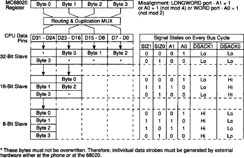
FIGURE 9.5 Misaligned long word transfer.
Finally, if the device is 32-bit, the device receives all 32-bit data $02A10512 via pins D31–D0 and asserts ![]() to indicate completion of the transfer. Aligned data transfers for various devices are shown in Figure 9.6.
to indicate completion of the transfer. Aligned data transfers for various devices are shown in Figure 9.6.
Next, consider a misaligned transfer such as MOVE.W D1,$02010741 with [Dl] = $20F107A4. The 68020 outputs $0707A4XX on its D31–D0 pins in its first cycle, where the XX are don't cares. Data transfers to various devices are summarized in Figure 9.7.
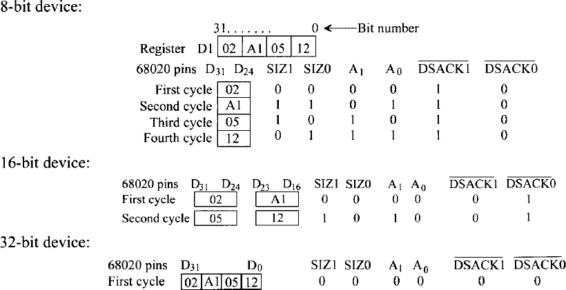
FIGURE 9.6 Aligned data transfers.
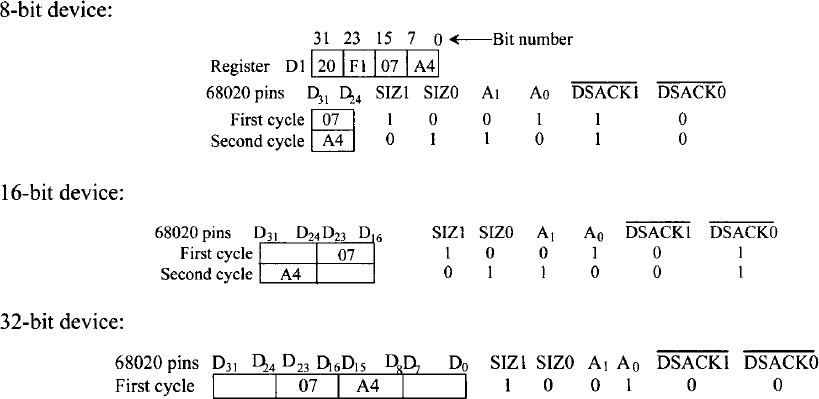
FIGURE 9.7 Misaligned data transfers.

FIGURE 9.8 Solution for Example 9.2.
EXAMPLE 9.2 Determine the number of bus cycles, the bytes written to memory (in hex), and signal levels of A1, A0, ![]() ,
, ![]() , SIZ1, and SIZ0 pins that would occur when the instruction MOVE.L D1,(A0) with [D1] = $50126124 and [A0] = $20002053 is executed by the MC68020. Assume:
, SIZ1, and SIZ0 pins that would occur when the instruction MOVE.L D1,(A0) with [D1] = $50126124 and [A0] = $20002053 is executed by the MC68020. Assume:
- (a) 32-bit memory
- (b) 16-bit memory
- (c) 8-bit memory
SolutionSee Figure 9.8.
9.1.3 68020 Timing Diagrams
Figure 9.9(a) and (b) show typical 68020 read and write timing diagrams (general form). The read and write cycle parameter specifications are provided in Table 9.1.
Note that in Figure 9.9, signals such as SIZ1, SIZ0, ![]() ,
, ![]() , D0- D31, A1 and A0 which distinguish data transfers between 8-, 16-, and 32-bit devices, are kept in general form. A simplified explanation of the read and write timing diagrams of Figures 9.9(a) and (b) are provided in the following.
, D0- D31, A1 and A0 which distinguish data transfers between 8-, 16-, and 32-bit devices, are kept in general form. A simplified explanation of the read and write timing diagrams of Figures 9.9(a) and (b) are provided in the following.
Consider the read timing diagram of Figure 9.9(a). In response to executing a read instruction such as MOVE.L $50207080,D0 (address chosen arbitrarily), the 68020 places the 32-bit address on the A31 - A0 pins during S0, outputs LOW on ![]() and
and ![]() during S1, and places a HIGH on the
during S1, and places a HIGH on the ![]() pin during S0, indicating a read operation. The 68020 then samples
pin during S0, indicating a read operation. The 68020 then samples ![]() and
and ![]() at the falling edge of S2 (two cycles). The pins
at the falling edge of S2 (two cycles). The pins ![]() and
and ![]() are asserted as 00 (32-bit memory) by the external memory using parameter 31a of Table 9.7. Hence, no wait state(s) are required. Assuming that the data is placed on the 68020's D31 - D0 pins, the 68020 reads data approximately at the falling edge of S4 (three cycles). Note that all other relevant 68020 signals required during the read operation shown in Figure 9.9(a) satisfy the timing parameters according to the specifications of Table 9.7.
are asserted as 00 (32-bit memory) by the external memory using parameter 31a of Table 9.7. Hence, no wait state(s) are required. Assuming that the data is placed on the 68020's D31 - D0 pins, the 68020 reads data approximately at the falling edge of S4 (three cycles). Note that all other relevant 68020 signals required during the read operation shown in Figure 9.9(a) satisfy the timing parameters according to the specifications of Table 9.7.
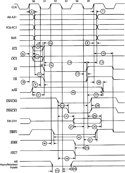

TABLE 9.7 Read and Write Cycle Specifications
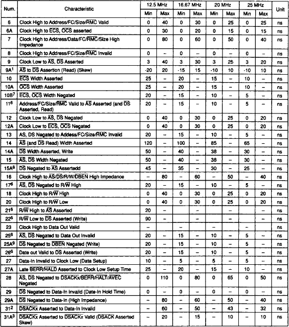

Next, consider the write timing diagram of Figure 9.9(b). In response to executing a write instruction such as MOVE.L D0,$50708000 (address arbitrarily chosen), the 68020 outputs the 32-bit address on the A31 - A0 pins during S0, outputs LOW on ![]() during S2, and places a LOW on the
during S2, and places a LOW on the ![]() pin during S0, indicating a write operation. The 68020 then samples
pin during S0, indicating a write operation. The 68020 then samples ![]() and
and ![]() at the falling edge of S2 (two cycles). The pins
at the falling edge of S2 (two cycles). The pins ![]() and
and ![]() are asserted as 00 (32-bit memory) by the external memory using parameter 31a of Table 9.7. The 68020 places data on its D31 - D0 pins during S2, and then asserts
are asserted as 00 (32-bit memory) by the external memory using parameter 31a of Table 9.7. The 68020 places data on its D31 - D0 pins during S2, and then asserts ![]() LOW using parameter 26 of Table 9.7. The external memory then writes the data into the addressed memory location. Note that all other relevant 68020 signals required during the write operation shown in Figure 9.9(b) satisfy the timing parameters according to the specifications of Table 9.7.
LOW using parameter 26 of Table 9.7. The external memory then writes the data into the addressed memory location. Note that all other relevant 68020 signals required during the write operation shown in Figure 9.9(b) satisfy the timing parameters according to the specifications of Table 9.7.
9.2 68020 System Design
This section contains 68020 interfacing to 27C256 EPROM, LH62256C/CH SRAM, and 68230 I/O chips. Memory and I/O maps are also determined. As mentioned before, the 68020 uses only asynchronous bus cycles in which ![]() ,
, ![]() , and
, and ![]() pins are used as handshaking signals for data transfers. Also, for 16-bit or 32-bit memory or I/O chips, the correct byte enable must be produced to ensure that appropriate memory or I/O chip(s) is enabled.
pins are used as handshaking signals for data transfers. Also, for 16-bit or 32-bit memory or I/O chips, the correct byte enable must be produced to ensure that appropriate memory or I/O chip(s) is enabled.

Note that both supervisor and user memory are needed for multitasking or multiuser systems. However, one can design memory without using the FC2, FC1, and FCO pins in memory decoding logic for a single application or for systems requiring no operating systems. In that case, the 68000 will always operate in the supervisor mode. Upon hardware reset, the 68020 will operate in the supervisor mode and will continue to operate in that mode.
9.2.1 Memory Decode Logic for Memory and I/O
In the following, an 8-MHz 68020 is used. The system will contain four 27C256s (32K × 8 HCMOS EPROM with 120-ns access time) and four LH2256C/CHs (32K × 8 CMOS SRAM with 70 ns speed). Because EPROM or SRAM is 32 kB wide, the 68020 address lines A2–A16 are used to address the EPROMs or SRAMs. The 68020 SIZ1, SIZ0, A1, A0, ![]() , and
, and ![]() pins are utilized for selecting the memory chips.
pins are utilized for selecting the memory chips.
Since the 68000 uses memory-mapped I/O, an unused address pin must be used to distinguish between memory and I/O. To keep things simple, only one 68230 is used in this design. The 68020 A17 pin will be used to select memory or I/O. A17 = 0 will select the memory chips and A17 = 1 will select the I/O chip. The 68020 A18, on the other hand, will be used to select EPROM or SRAM. A18= 0 will select 27C256, whereas A18 = 1 will select 2256C/CH. Pins A17 and A18 are chosen arbitrarily. The memory and I/O decoding is listed in Table 9.8.
To manipulate memory configuration, 32-bit data bus control byte enable logic is incorporated to generate byte enable signals (![]() ,
, ![]() ,
, ![]() , and
, and ![]() ). These byte enables are generated by using 68020's SIZ1, SIZ0, A1, A0, and
). These byte enables are generated by using 68020's SIZ1, SIZ0, A1, A0, and ![]() pins, as shown in the individual logic diagrams of the byte enable logic. An FPGA can be programmed to implement this logic.
pins, as shown in the individual logic diagrams of the byte enable logic. An FPGA can be programmed to implement this logic.
TABLE 9.9 Memory Enables for 32-Bit Memory
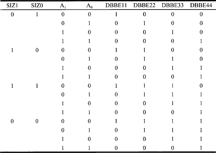
Table 9.9 shows the memory enables for the 32-bit memory. Figure 9.10 shows the K-maps for the enable logic. A logic diagram can be drawn for generating the memory byte enable signals ![]() ,
, ![]() ,
, ![]() , and
, and ![]() .
.
9.2.2 68020-27C256 Interface
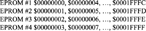
The 68020 system with 32-bit EPROM consists of four 27C256s, each connected to its associated portion of the system data bus (D3–D24, D23–Dl6, D15–D8, and D7–D0). 68020 pins A2 through A16 are connected to A0 through A14 of each 27C256. For example, 68020 A2 is connected to A0 of 27C256s, 68020 A3 to A, of the 27C256s, and so on. A schematic of the 68020–27C256 interface is shown in Figure 9.11. Linear decoding is used for selecting memory banks to enable the appropriate memory chips. Figure 9.12 obtained from Figure 9.11 shows the 68020 interface to EPROM #1. The 27C256 memory map can be determined from Figure 9.12 as follows:
EPROM #1

Note that the A0 pin of EPROM # 1 is connected to the 68020 A2 pin, A1 pin of EPROM # 1 is connected to the 68020 A3 pin, and so on. Hence the address range for EPROM #1:
$00000000, $00000004, …, $0001FFFC and the 27C256 memory map:
![]() and
and ![]() are generated by ANDing the
are generated by ANDing the ![]() ,
, ![]() ,
, ![]() , and
, and ![]() outputs of the byte enable logic circuit. When one or more EPROM chips are selected, the appropriate enables
outputs of the byte enable logic circuit. When one or more EPROM chips are selected, the appropriate enables ![]() will be low, thus asserting
will be low, thus asserting ![]()
![]() and
and ![]() . This will tell the 68020 that the memory is 32 bits wide. Data from the selected memory chip(s) will be placed on the appropriate data pins of the 68020.
. This will tell the 68020 that the memory is 32 bits wide. Data from the selected memory chip(s) will be placed on the appropriate data pins of the 68020.
Let us discuss the timing requirements of the 68020-27C256 system. In response to execution of a READ instruction such as MOVE.L $00001234,D0, the 68020 checks ![]() and
and ![]() for LOW at the falling edge of S2 (two cycles). From the 68020 timing diagram (in the Motorola manual),
for LOW at the falling edge of S2 (two cycles). From the 68020 timing diagram (in the Motorola manual), ![]() ,
, ![]() , and all other output signals used in memory decoding go to LOW at the end of approximately one clock cycle. For an 8-MHz 68020 clock, each cycle is 125 ns. From byte enable logic diagrams, a maximum of four gate delays (40 ns) are required. Therefore, the EPROM(s) selected will be enabled after 165 ns (125 ns + 40 ns). With a 90-ns access time for the 27C256, the EPROM(s) will place data on the output lines after approximately 255 ns (165 ns + 90 ns). With an 8-MHz 68020 clock,
, and all other output signals used in memory decoding go to LOW at the end of approximately one clock cycle. For an 8-MHz 68020 clock, each cycle is 125 ns. From byte enable logic diagrams, a maximum of four gate delays (40 ns) are required. Therefore, the EPROM(s) selected will be enabled after 165 ns (125 ns + 40 ns). With a 90-ns access time for the 27C256, the EPROM(s) will place data on the output lines after approximately 255 ns (165 ns + 90 ns). With an 8-MHz 68020 clock, ![]() and
and ![]() will be checked for LOW (32-bit memory) after two cycles (250 ns), and if LOW, the 68020 will latch data after three cycles (375 ns). Hence, no delay circuit is required for
will be checked for LOW (32-bit memory) after two cycles (250 ns), and if LOW, the 68020 will latch data after three cycles (375 ns). Hence, no delay circuit is required for ![]() and
and ![]() . In case a delay circuit is required for the 68020 with a higher clock frequency, a ring counter can be used.
. In case a delay circuit is required for the 68020 with a higher clock frequency, a ring counter can be used.

FIGURE 9.10 K-maps for enable signals for memory.
9.2.3 68020- 2256C/CH (SRAM) Interface
The Sharp LH2256C/CH is a 32K × 8 CMOS SRAM. The 2256C/CH READ and WRITE operations are decoded shown in Table 9.10. The 68020 system with 32-bit SRAM consists of four 2256C/CHs, each connected to its associated portion of the system data bus (D3–D24, D23–D16, D15–D8, and D7–D0). 68020 pins A2 through Al6 are connected to A0 through A14 of each 2256C/CH. For example, 68020 A2 is connected to A0of the 2256C/CHs, 68020 A3 to A1 of the 2256C/CHs, and so on. A schematic of the 68020–2256C/CH interface is shown in Figure 9.13.
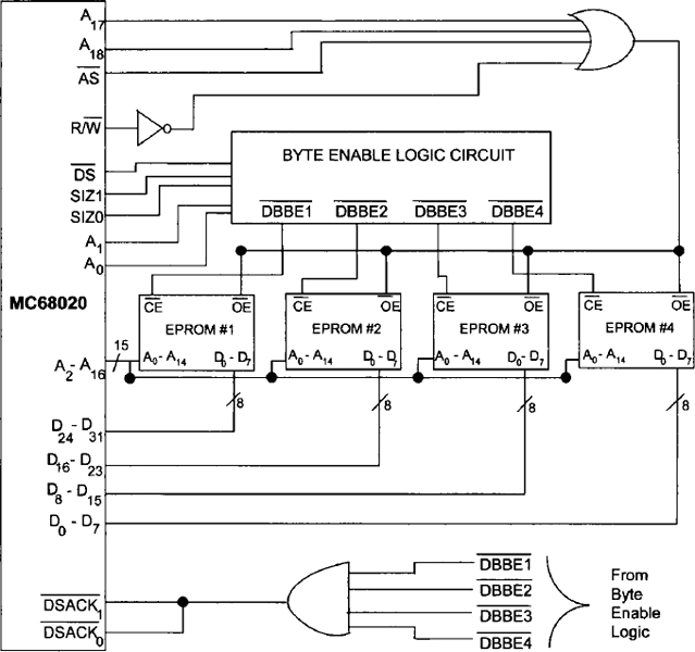
FIGURE 9.11 68020-27C256 interface.

FIGURE 9.12 68020 interface to EPROM #1.

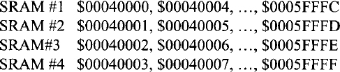
Linear decoding is used for selecting memory banks to enable the appropriate memory chips. Figure 9.14 obtained from Figure 9.13 shows the 68020 interface to SRAM #1. The SRAM #1 memory map can be determined from Figure 9.14 as follows:
SRAM #1

Note that the A0 pin of SRAM # 1 is connected to the 68020's A2 pin, the A1 pin of SRAM # 1 is connected to the 68020's A3 pin, and so on. Hence, the address range for SRAM #1: $00040000, $00040004, …, $0005FFFC.
Hence, the 62256C memory map:
As with EPROMs, ![]() and
and ![]() are generated by ANDing the
are generated by ANDing the ![]() ,
, ![]() ,
, ![]() , and
, and ![]() outputs of the byte enable logic circuit. When one or more SRAM chips are selected, the appropriate enables
outputs of the byte enable logic circuit. When one or more SRAM chips are selected, the appropriate enables ![]() will be low, thus asserting
will be low, thus asserting ![]() and
and ![]() . This will tell the 68020 that the memory is 32 bits wide. Data from the memory chip(s) selected will be placed on the appropriate data pins of the 68020. Also, it can be shown that no delay circuits for
. This will tell the 68020 that the memory is 32 bits wide. Data from the memory chip(s) selected will be placed on the appropriate data pins of the 68020. Also, it can be shown that no delay circuits for ![]() and
and ![]() are required since the 2256C/CH has read and write times of 70 ns each.
are required since the 2256C/CH has read and write times of 70 ns each.
9.2.4 68020 Programmed I/O
The 68020 I/O-handling features are very similar to those of the 68000. This means that the 68020 uses memory-mapped I/O, and the 68230 I/O chip can be used for programmed I/O. In the hardware schematic for the 68020-68230 interface shown in Figure 9.15,A17 is chosen to be HIGH to select the 68230 chip so that the port addresses are different from the 68020 reset vector addresses 0000000016 – 0000000616. The 68230 ![]() is an open-drain output. Hence, a pull-up resistor is required.
is an open-drain output. Hence, a pull-up resistor is required. ![]() is used to assert
is used to assert ![]() for indicating 8-bit I/O. Table 9.11 shows some of the 68230 register definitions.
for indicating 8-bit I/O. Table 9.11 shows some of the 68230 register definitions.
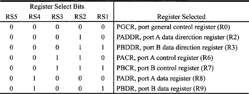
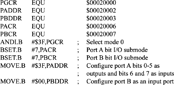
Let us now determine the I/O map. Note that A31 through A18, and A16 through A5 are don't cares and are assumed to be 0's in the following. Also, A17 = 1 for I/O. Hence, from the figure, addresses for registers PGCR (R0), PADDR (R2), PBDDR (R3), PACR (R6), PBCR (R7), PADR (R8), and PBDR (R9) can be obtained as shown below. For example, consider PGCR as follows:
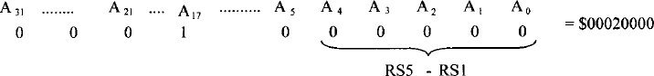

FIGURE 9.13 68020/2256C/CH interface.

FIGURE 9.14 68020 interface to SRAM #1.
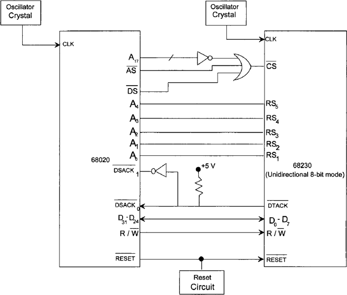
FIGURE 9.15 68020/68230 interface.
Therefore, address for PGCR = $00020000. Similarly, address for PADDR = $00020002, address for PBDDR = $00020003, address for PACR = $00020006, address for PBCR = $00020007 address for PADR =$00020008, address for PBDR =$00020009.
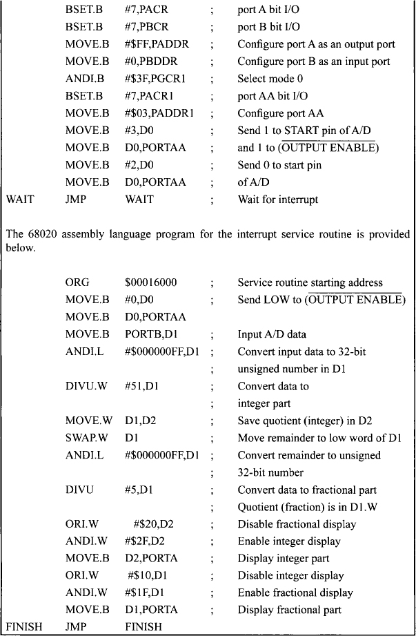
As an example, the following instruction sequence will select mode 0, submode IX, and configure bits 0–5 of Port A as outputs, bits 6 and 7 of Port A as inputs, and port B as an input port:
TABLE 9.11 Some 68230 Registers
9.3 68020 Exception processing
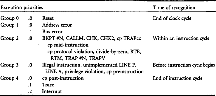
The 68020 exceptions are functionally similar to those of the 68000 with some minor variations. The 68020 exceptions can be generated by external or internal causes. Externally generated exceptions include interrupts, bus errors, reset, and coprocessor-detected errors. Internally generated exceptions are caused by certain instructions, address errors, tracing, and breakpoints. Instructions that may cause internal exceptions as part of their instruction execution are CHK, CHK2, CALLM, RTM, RTE, DIV, and all variations of the TRAP instructions. In addition, illegal instructions, privilege violations, and coprocessor violations cause exceptions. Table 9.12 lists the priority and characteristics of all 68020 exceptions.
The 68020 exception processing is similar to the 68000 with some minor variations. In the 68020, exception processing occurs in four steps and varies according to the cause of the exception. The four steps are summarized below:
1. An internal copy is made of the SR, and the S-bit set is to 1 for exception processing. This means that the 68020 enters the supervisor state and tracing is disabled.
2. The vector number of the exception vector is determined from either the exception-requesting peripheral (nonautovector) or internally upon assertion of the ![]() (autovector) input. Note that in the 68000,
(autovector) input. Note that in the 68000, ![]() is asserted for autovectoring. The VBR register points to the base of the 1-kB exception vector table, which contains 256 exception vectors. The 68020 uses exception vectors as memory pointers to fetch the starting address of service routines that handle the various exceptions.
is asserted for autovectoring. The VBR register points to the base of the 1-kB exception vector table, which contains 256 exception vectors. The 68020 uses exception vectors as memory pointers to fetch the starting address of service routines that handle the various exceptions.
3. The processor saves PC and SR onto the supervisor stack. For coprocessor exceptions, additional internal state information is saved on the stack as well.
4. The final step is the same for all exceptions. The exception vector is determined by multiplying the vector number by 4, and adding it to the contents of the VBR to determine the memory address of the exception vector. The PC (and ISP for reset exception) is loaded with the exception vector. The instruction located at the address given in the exception vector is fetched and the exception-handling routine is thus executed.
Exception processing saves certain information on the top of the supervisor stack. This information is called the exception stack frame.
The 68020 provides six different stack frames. The sizes of these frames vary from four words to 46 words depending on the exception. For example, the normal four-word stack frame is generated by exceptions such as interrupts and privilege violations. A six-word stack frame is generated by instruction-related exceptions such as CHK/CHK2 and zero divide.
The 68020 utilizes the concept of two supervisor stacks pointed to by MSP and ISP. The M-bit (when S = 1) determines the active supervisor stack pointer. The 68020 accesses MSP when S = 1, M = 0. The MSP can be used for program traps and other exceptions, while the ISP can be used for interrupts. The use of two supervisor stacks allows isolation of user processes or tasks and asynchronous supervisor I/O tasks.
The 68020 ![]() ,
, ![]() ,
, ![]() ,
, ![]() , and
, and ![]() pins are used as the 68020 hardware interrupt control signals (Figure 9.16). Like the 68000, the 68020 supports seven levels of prioritized interrupts encoded by using the
pins are used as the 68020 hardware interrupt control signals (Figure 9.16). Like the 68000, the 68020 supports seven levels of prioritized interrupts encoded by using the ![]() ,
, ![]() , and
, and ![]() pins.
pins.
In Figure 9.16, when interrupting priority levels 1 through 6 are requested, the 68020 compares the interrupt level (inverted interrupt pins) to the interrupt mask to determine whether the interrupt should be processed. An interrupt recognized as valid does not force immediate exception processing; a valid interrupt causes ![]() to be asserted, signaling to external devices that the 68020 has an interrupt pending. The deskew logic in Figure 9.17 continuously samples the
to be asserted, signaling to external devices that the 68020 has an interrupt pending. The deskew logic in Figure 9.17 continuously samples the ![]() ,
, ![]() , and
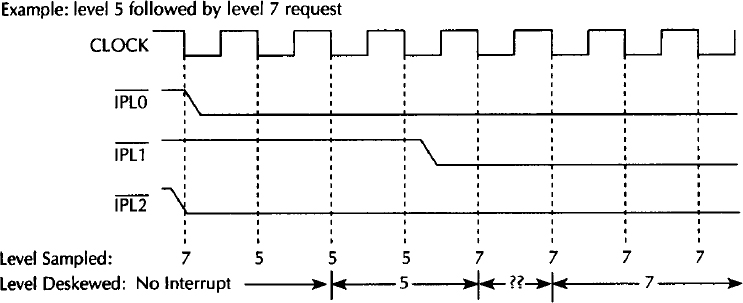
, and ![]() pins on every falling edge of the clock, but deskews or latches an interrupt request when it remains at the same level for two consecutive falling edges of the input clock. Figure 9.17 gives an example of the 68020 interrupt deskewing logic.
pins on every falling edge of the clock, but deskews or latches an interrupt request when it remains at the same level for two consecutive falling edges of the input clock. Figure 9.17 gives an example of the 68020 interrupt deskewing logic.
Whenever the 68020 reaches an instruction execution boundary, it checks for a pending interrupt. If it finds one, the 68020 begins an exception processing and executes an interrupt acknowledge cycle with FC2, FC1, FC0 =111, and A19,A18,A17,A16= 1111. The 68020 basic hardware interrupt sequence is shown in Figure 9.18.
Figure 9.19 shows the interrupt acknowledge flowchart. Before the interrupt acknowledge cycle is completed, the 68020 must receive either ![]() ,
, ![]() , or
, or ![]() ; otherwise, it will execute wait states until one of these input pins is activated externally.
; otherwise, it will execute wait states until one of these input pins is activated externally.
If ![]() is asserted, the 68020 obtains the vector address internally (autovectored) automatically. If the 68020
is asserted, the 68020 obtains the vector address internally (autovectored) automatically. If the 68020 ![]() pins are asserted, the 68020 takes an 8-bit vector from the appropriate data lines (D7–D0 pins for a 32-bit device, D23–D16 pins for a 16-bit device, D31–D24 pins for an 8-bit device). These are nonautovectored interrupts, and the 68020 obtains the interrupt vector address by adding VBR with 4 * (8-bit vector).
pins are asserted, the 68020 takes an 8-bit vector from the appropriate data lines (D7–D0 pins for a 32-bit device, D23–D16 pins for a 16-bit device, D31–D24 pins for an 8-bit device). These are nonautovectored interrupts, and the 68020 obtains the interrupt vector address by adding VBR with 4 * (8-bit vector).
Figure 9.20 shows an example of autovectored and nonautovectored interrupt logic. Finally, if ![]() is asserted, the interrupt is considered spurious and the 68020 assigns the appropriate vector number for handling this.
is asserted, the interrupt is considered spurious and the 68020 assigns the appropriate vector number for handling this.
9.4 68020-based Voltmeter
A 68020-based voltmeter is designed in this section. A 68020/27C256/62256/68230-based microcomputer is used to implement the voltmeter to measure voltage in the range 0 to 5 V and display the result in two decimal digits: one integer part and one fractional part. The microcomputer will contain 16-bit I/O and will use two 68230 I/O chips; one containing even port addresses and the other containing odd port addresses. Three 8-bit I/O ports are used in the design. The two 8-bit ports (ports A and B) of the even 68230, and the 8-bit port (port A) of the odd 68230 will be used.
The 68230 port addresses are chosen arbitrarily and are given below.
- Ports used from the even 68230: PGCR = $00002000, PACR = S0000200C, PBCR = S0000200E, PADDR = $00002004, PBDDR = $00002006, PADR = $00002010= port A, and PBDR = $00002012 = port B.
TABLE 9.12 Exception Priorities and Recognition Times
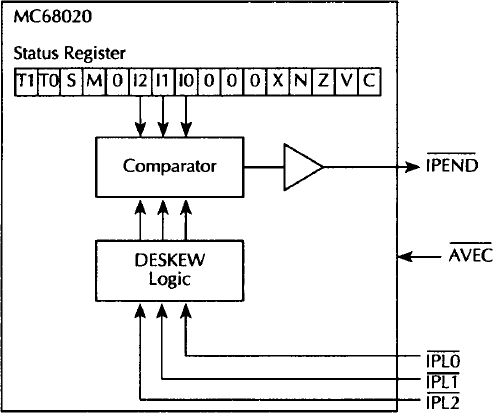
FIGURE 9.16 68020 interrupt control signals.
- Ports used from the odd 68230: PGCR1 = $00002001, PACR1 = $0000200D, PADDR1= $00002005, and PADR1 = $00002011 = port AA.

The 68020-based voltmeter will be designed using both programmed I/O, and interrupt I/O (nonmaskable and maskable).
9.4.1 Voltmeter Design Using Programmed I/O
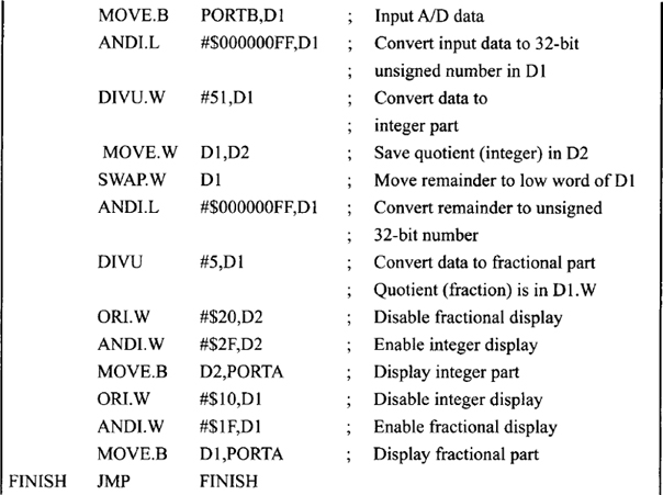
Figure 9.21 shows the schematic of the voltmeter using the 68020-based microcomputer. The microcomputer is required to start the A/D converter at the falling edge of a pulse via bit 0 of port AA. When the conversion is completed, the A/D's CONVERSION COMPLETE signal will go to HIGH. During the conversion, the A/D's CONVERSION COMPLETE signal stays LOW.

FIGURE 9.19 Interrupt acknowledge sequence flowchart.

FIGURE 9.20 68020 autovectored and nonautovectored interrupt logic.
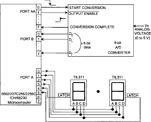
FIGURE 9.21 68020-based voltmeter using programmed I/O.
Using programmed I/O, the microcomputer will poll the A/D's CONVERSION COMPLETE signal. When the conversion is completed, the microcomputer will send a LOW on the A/D converter's ![]() line via bit 1 to port AA and then input the 8-bit output from A/D via port B and display the voltage (0 to 5 V) in two decimal digits (one integer and one fractional) via port A on two TIL 311 displays. Note that the TIL 311 has an on-chip BCD-to-seven-segment decoder. The microcomputer will output each decimal digit on the common lines (bits 0–3 of port A) connected to the ABCD inputs (‘A’ is the least significant bit and ‘D’ is the most significant bit) of the displays. Each display will be enabled by outputting LOW on each
line via bit 1 to port AA and then input the 8-bit output from A/D via port B and display the voltage (0 to 5 V) in two decimal digits (one integer and one fractional) via port A on two TIL 311 displays. Note that the TIL 311 has an on-chip BCD-to-seven-segment decoder. The microcomputer will output each decimal digit on the common lines (bits 0–3 of port A) connected to the ABCD inputs (‘A’ is the least significant bit and ‘D’ is the most significant bit) of the displays. Each display will be enabled by outputting LOW on each ![]() line in sequence (one after another) so that the input voltage Vx (0 to 5 V) will be displayed with one integer part and one fractional part. A 68020 assembly language program will accomplish this.
line in sequence (one after another) so that the input voltage Vx (0 to 5 V) will be displayed with one integer part and one fractional part. A 68020 assembly language program will accomplish this.
Because the maximum decimal value that can be accommodated in 8 bits is 25510 (FF16), the maximum voltage of 5 V will be equivalent to 25510. This means the display in decimal is given by
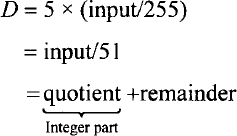
This gives the integer part. The fractional part in decimal is

For example, suppose that the decimal equivalent of the 8-bit output of A/D is 200.
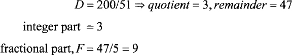
Therefore, the display will show 3.9 V. The 68020 assembly language program using programmed I/O can be written as follows:


9.4.2 Voltmeter Design Using Interrupt I/O
In this section the 68020-based voltmeter is designed using interrupt I/O (both nonmaskable and maskable). The main program is written to initialize the 68230 control registers and then start the A/D. The service routine will input the A/D data, display the result, and stop. A 68020 assembly language program is written for both the main program and the service routine.
Using Autovector Level 7 (Nonmaskable Interrupt) Figure 9.22 shows the pertinent connections for Autovector level 7 interrupt. The A/D CONVERSION COMPLETE signal is inverted, and then connected to 68020 ![]()
![]()
![]() pins and to the
pins and to the ![]() pin. Note that all addresses selectable by the user are chosen arbitrarily in the following.
pin. Note that all addresses selectable by the user are chosen arbitrarily in the following.
The main programs and service routines are written at addresses $00005000 and $00016000, respectively. Also, the interrupt stack pointer A7' is initialized at $00006500. These addresses are chosen arbitrarily. The main program in 68020 assembly language is shown below.
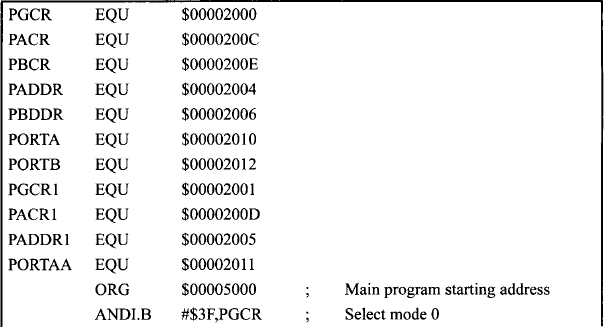

FIGURE 9.22 68020-based voltmeter using nonmaskable interrupt I/O.
Using 68020 assembler directive DC.L, the reset and service routine vectors can be written as follows:
Reset Vector
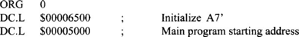
Service routine vector for nonmaskable interrupt (autovector level 7):
![]()
Note that in the above it is assumed that [VBR] = 0. Hence, the vector address for autovector level 7 is S0000007C.
Using Nonautovectoring (Maskable Interrupt, Vector $40) Figure 9.23 shows the pertinent connections for the nonautovectoring interrupt. All connections for the A/D converter to ports AA and B and seven-segment displays to port A of the 68020-based microcomputer in Figure 9.23 will be the same as shown in Figure 9.21. The 68020 ![]() ,
, ![]() ,
, ![]() pins are connected in such a way that
pins are connected in such a way that ![]() ,
, ![]() ,
,![]() will interrupt the 68020 as 001 (level 1 interrupt) since the
will interrupt the 68020 as 001 (level 1 interrupt) since the ![]() ,
, ![]() , and
, and ![]() pins are inverted internally. In response to the interrupt, the 68000 automatically pushes PC and SR onto the stack and generates FC2, FC1,FC0= 111 (CPU space cycle) and A19, A18,A17, A16= 1111, indicating acknowledgment of the interrupt. These seven signals are NANDed in the figure to generate a LOW interrupt acknowledge signal, which is used to enable an octal buffer such as 74HC244.
pins are inverted internally. In response to the interrupt, the 68000 automatically pushes PC and SR onto the stack and generates FC2, FC1,FC0= 111 (CPU space cycle) and A19, A18,A17, A16= 1111, indicating acknowledgment of the interrupt. These seven signals are NANDed in the figure to generate a LOW interrupt acknowledge signal, which is used to enable an octal buffer such as 74HC244.
Vector number 4016 can be placed at the input of the octal buffer as shown in the figure. A value of 10 is asserted at the 68020 ![]() and
and ![]() pins so that the 68020 will recognize the device as 8-bit and will input the vector number via the 68020's D31- D24 pins. Hence, the output pins of the octal buffer are connected to the 68020,s D31-D24 pins.
pins so that the 68020 will recognize the device as 8-bit and will input the vector number via the 68020's D31- D24 pins. Hence, the output pins of the octal buffer are connected to the 68020,s D31-D24 pins.
The main programs and service routines are written at addresses $00005000 and $00016000 respectively. Also, the interrupt stack pointer A7' is initialized at $00006500. These addresses are chosen arbitrarily. The main program in 68020 assembly language is provided below.

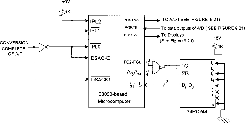
FIGURE 9.23 68020-based voltmeter using maskable interrupt I/O.

Using 68020 assembler directive DC.L, the reset and service routine vectors can be written as follows:
Reset Vector:
Starting address for the maskable interrupt ( vector number $40):
![]()
Note above that it is assumed that [VBR] = 0. The vector address for vector # 40 = 4 * $40 = $100. Hence, the 32-bit address $00000100 is used as the starting address of the service routine.
9.5 Interfacing a 68020-Based Microcomputer to a Hexadecimal Keyboard and a Seven-Segment Display
In this section we describe the basics of interfacing a 68020-based microcomputer to a hexadecimal keyboard and a seven-segment display.
9.5.1 Basics of Keyboard and Display Interface to a Microcomputer
A common method of entering programs into a microcomputer is via a keyboard way of displaying microcomputer results is by using seven-segment displays, functions to be performed for interfacing a keyboard are:
- Sense a key actuation.
- Debounce the key.
- Decode the key.
Let us now elaborate on keyboard interfacing concepts. A keyboard is arranged in rows and columns. Figure 9.24 shows a 2 × 2 keyboard interfaced to a typical microcomputer. In Figure 9.24 the columns are normally at a HIGH level. A key actuation is sensed by sending a LOW (closing the diode switch) to each row one at a time via PA0 and PA1 of port A. The two columns can then be input via PB2 and PB3 of port B to see whether any of the normally HIGH columns are pulled LOW by a key actuation. If so, the rows can be checked individually to determine the row in which the key is down. The row and column code for the key pressed can thus be found.
The next step is to debounce the key. Key bounce occurs when a key is pressed or released—it bounces for a short time before making the contact. When bounce occurs, it may appear to the microcomputer that the same key has been actuated several times instead of just once. This problem can be eliminated by reading the keyboard after about 20 ms and then verifying to see if it is still down. If it is, the key actuation is valid. The next step is to translate the row and column code into a more popular code, such as hexadecimal or ASCII. This can easily be accomplished by a program. Certain characteristics associated with keyboard actuations must be considered while interfacing to a microcomputer. Typically, these are two-key lockout and N-key rollover. The two-key lockout ensures that only one key is pressed. An additional key depressed and released does not generate any codes. The system is simple to implement and most often used. However, it might slow down the typing because each key must be released fully before the next one is pressed down. On the other hand, the N-key rollover will ignore all keys pressed until only one remains down.
Now let us elaborate on the interfacing characteristics of typical displays. The following functions are typically performed for displays:
- Output the appropriate display code.
- Output the code via right entry or left entry into the displays if there is more than one display.
These functions can easily be realized by a microcomputer program. If there is more than one display, the displays are typically arranged in rows. A row of four displays is shown in Figure 9.25. In the figure, one has the option of outputting the display code via right entry or left entry. If the code is entered via right entry, the code for the least significant digit of the four-digit display should be output first, then the next-digit code, and so on. The program outputs to the displays are so fast that visually all four digits will appear on the display simultaneously. If the displays are entered via left entry, the most significant digit must be output first and the rest of the sequence is similar to that of right entry.
Two techniques are typically used to interface a hexadecimal display to the microcomputer: nonmultiplexed and multiplexed. In nonmultiplexed methods, each hexadecimal display digit is interfaced to the microcomputer via an I/O port. Figure 9.26 illustrates this method. BCD-to-seven-segment conversion is done in software. The microcomputer can be programmed to output to the two display digits in sequence. However, the microcomputer executes the display instruction sequence so fast that the displays appear to the human eye at the same time. Figure 9.27 illustrates the multiplexing method of interfacing the two hexadecimal displays to the microcomputer. In the multiplexing scheme, appropriate seven-segment code is sent to the desired displays on seven lines common to all displays. However, the display to be illuminated is grounded. Some displays, such as Texas Instrument's TIL 311, have an on-chip decoder. In this case, the microcomputer is required to output 4 bits (decimal) to a display.
The keyboard and display interfacing concepts described here can be realized by either software or hardware. To relieve the microprocessor of these functions, microprocessor manufacturers have developed a number of keyboard/display controller chips. These chips are typically initialized by the microprocessor. The keyboard/display functions are then performed by the chip independent of the microprocessor. The number of keyboard/display functions performed by the controller chip varies from one manufacturer to another. However, these functions are usually shared between the controller chip and the microprocessor.

FIGURE 9.24 Typical microcomputer-keyboard interface.
![]()
FIGURE 9.25 Row of four displays.

FIGURE 9.26 Nonmultiplexed hexadecimal displays.

FIGURE 9.27 Multiplexed displays
9.5.2 68020 Interface to a Hexadecimal Keyboard and a Seven-Segment Display
In this section a 68020-based microcomputer is designed to display a hexadecimal digit entered via a keypad (16 keys). The microcomputer will contain 16-bit I/O and will use two 68230 I/O chips; one containing even port addresses and the other containing odd port addresses. Three 8-bit I/O ports are used in the design. The two 8-bit ports (ports A and B) of the even 68230 and the 8-bit port (port A) of the odd 68230 will be used.
Figure 9.27 shows the hardware schematic. Ports A, B, and AA are configured as follows:
- Port A is configured as an input port to receive the row–column code.
- Port B is configured as an output port to display the key(s) pressed.
- Port AA is configured as an output port to output zeros to the rows to detect a key actuation.
The 68230 port addresses are chosen arbitrarily, and are provided in the following:
Ports used from the even 68230: PGCR = $00002000, PACR = $0000200C, PBCR = $0000200E, PADDR = $00002004, PBDDR = $00002006, PADR = $00002010= port A, and PBDR = $00002012 = port B.
Ports used from the odd 68230: PGCR1 = $00002001, PACR1 = $0000200D, PADDR1 = $00002005, and PADR1 = $00002011 = port AA.
The 68020 is assumed to run at 8 MHz. Debouncing is provided to avoid unwanted oscillation caused by the opening and closing of key contacts. To ensure stability for the input signal, a delay of 20 ms is used for debouncing the input.
Typical 68020 software delay loops can be written using MOVE and DBF instructions. For example, the following instruction sequence can be used for a delay loop of 2 ms:
![]()
Note that DBF.W in the above decrements D0.W by 1, and if D0.W ≠ −1, branches to DELAY; if D0.W = −1, the 68020 executes the next instruction. Since DBF.W checks for D0.W for −1, the value of “count” must be one less than the required loop count. The initial loop counter value of “count” can be calculated using the cycles (see the Motorola 68020 manual) required to execute the following 68000 instructions:

Note that DBF.W requires 10 cycles when the 68020 branches if the content of D0.W is not equal to −1 after autodecrementing D0.W by 1. However, the 68020 goes to the next instruction and does not branch when [D0.W] = −1 after autodecrementing D0.W by 1, and this also requires 10 cycles. This means that the DELAY loop will require 10 cycles for “(count + 1)” times.
Assuming an 8-MHz 68020 clock, each cycle is 125 ns. For a 2-ms delay, total ![]() . Hence, total cycles including the MOVE.W = 3 + 10 × (count + 1) = 16,000. Hence, count ≅ 1599. Therefore, D0.W must be loaded with 159910 for a 2-msec delay.
. Hence, total cycles including the MOVE.W = 3 + 10 × (count + 1) = 16,000. Hence, count ≅ 1599. Therefore, D0.W must be loaded with 159910 for a 2-msec delay.
Now, to obtain a delay of 20 ms, the 2-ms DELAY loop above can be used with an external counter. Counter ![]() . The following instruction sequence will provide an approximate delay of 2 seconds:
. The following instruction sequence will provide an approximate delay of 2 seconds:
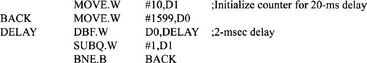
Note that the 68020 instruction sequence above will provide a delay of 20 ms discarding the execution times of MOVE.W #10,D1, SUBQ.W, and BNE.B instructions.
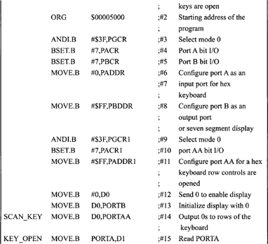
The 68020 assembly language program for interfacing the 68020-based microcomputer to a hexadecimal keyboard and a seven-segment display follows. Note that to explain the program, line numbers are included with the comments.
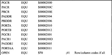

FIGURE 9.28 68020-based microcomputer interface to keyboard and display.
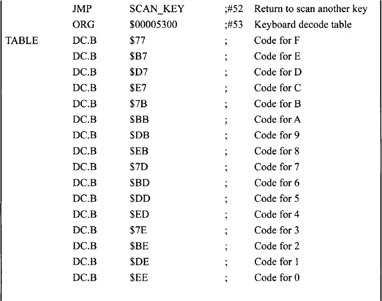
In the program, a decode table for keys 0 through F are stored at address $00005301 (chosen arbitrarily). The codes for the hexadecimal numbers 0 through F are obtained by inspecting Figure 9.28. For example, consider key F. When key F is pressed and if a LOW is output by the program to bit 0 of port AA, the top row and rightmost column of the keyboard will be LOW. This will make the content of port A:
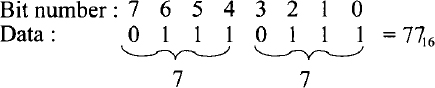
Thus, a code of 7716 is obtained at port A when key F is pressed. Diodes are connected at the 4 bits (bits 0-3) of port AA. This is done to make sure that when a 0 is output by the program to one of these bits (row of the keyboard), the diode switch will close and will generate a LOW on that row.
Now, if a key is pressed on a particular row that is LOW, the column connected to this key will also be LOW. This will enable the programmer to obtain the appropriate key code for each key.
Next, the assembly language program will be explained using the line numbers included in the comment field.
Line #1 equates label OPEN to data $F0. This is because when all keys are up (no keys are pushed) and 0's are output to the rows in Figure 9.28, data input at port A will be 11110000 ($F0). Note that bits 0 -3 are connected to rows and bits 4-7 are connected to columns of the keyboard. Line #2 includes the starting address of the program at $00005000. This address is chosen arbitrarily.
Lines 3 through 11 configure port A as input and ports B and AA as output ports. Lines 12 and 13 initialize the seven-segment display by outputting 0. Lines 14 through 17 check to see if any key is pushed. This is done by outputting 0's to all rows via port AA, and then inputting port A. If all keys are open, data at port A will be $F0. Hence, data at port A is compared with $F0. If Z = 0, the program waits in a loop with label KEY_OPEN until a key is pushed. When a key is closed, Z = 1, and the program comes out of the loop. Lines 18 through 22 debounce the keys by providing a delay of 20 ms.
Lines 23 through 25 detect a key closure. The program inputs port A and, compares input data with $F0. If Z = 1, the program waits in a loop with label KEY_CLOSE until a key is closed. If Z = 0, the program leaves the loop. Lines 26 through 30 provide debouncing if a key closure is detected. It is necessary to determine exactly which key is pressed. To do this, a sequence of row-control codes ($XE, $XD, $XB, and $X7, where X is don't care; the upper 4 bits are don't cares) are output via port AA. Lines 31 through 34 initialize D2.B to all 1's, clear the X-bit to 0, and rotate D2.B through X once to the left to contain the appropriate row control code. For example, after the first ROXL.B in line 33, D2.B will contain 11111110($FE). Note that the low 4 bits are the row-control code (the upper 4 bits are don't cares) for the first pass in the loop, labeled NEXT_ROW. Line 35 outputs this data to port AA to make the top row of the keyboard zero.
The row–column code is input via port A to determine if the column code changes corresponding to each different row code. Line 36 inputs port A into D2.B. The top row of the keyboard will be 0 if C or D or E or F is pushed. Line 37 saves this input data in D4.B.
Lines 38 through 40 make the low 4 bits 0's and retain the upper 4 bits. If the column code is not $F0 (changed), the input key is identified. The program then indexes through a look-up table to determine the row–column code saved in D0.B. If the code is found, the corresponding index value, which equals the input key's value (a single hexadecimal digit), is displayed.
Suppose that key F is pushed. Line 37 will store the code $77 in D4.B. The instruction CMPI.B at line 39 will make Z = 0. Hence, after execution of BNE.B at line 40, the program branches to DECODE (line 45). Lines 45 through 50 compare the key code saved in D4.B with $77 (data for F) stored at the address labeled TABLE ($00005300) in the decode table. Since there is a match, the Z-flag will be 1. The program comes out of the loop with the label SEARCH and outputs the character F to the seven-segment display at line 51.
However, if no key in the top row is pushed, a 0 is output to the second row, and the process continues. The program is written such that it will scan continuously for an input key and update the display for each new input. The memory and I/O maps are chosen arbitrarily.
Questions and Problems
| 9.1 | Why is the 68020 provided with multiple Vcc and ground pins? |
| 9.2 | What is the purpose of each of the following 68020 pins?
|
| 9.3 | If there are no interrupts or DMA required in a 68020-based application, identify whether you would connect each of the following 68020 pins to HIGH or LOW or keep it floating: |
| 9.4 | Identify the function performed by the 68020 when FC2, FC1, FC0 =111 and A19, A18, A17, A16 = 1111. |
| 9.5 | Assume a 25-MHz 68020 in Figure P9.5. Also, assume that data is ready at the output pins of the 32-bit device at 300 ns. For the timing diagram of Figure P9.5, determine the time at which data will be read by the 68020. |
| 9.6 | Assume the following data prior to execution of a 68020 hardware reset: [$00000000] = $00004000, [$00000004] = $10007000, [ISP] = $23457180, [PC] = $00405690, [VBR] = $12345678, [D4.L] = $45672368, and [SR] = $4020. Find the contents of the memory locations and/or registers affected. |
| 9.7 | What is 68020 dynamic bus sizing? |
| 9.8 | Consider the 68020 instruction MOVE.B D1,$00000016. Find the 68020 data pins over which data will be transferred if |
| 9.9 | If a 32-bit data is transferred using the 68020's MOVE.L D0,$50607011 instruction to a 32-bit memory with [D0] = $81F27561, how many bus cycles are needed to perform the transfer? What are A1 and A0 equal to during each cycle? What is the SIZ1,SIZ0 code during each cycle? What bytes of data are transferred during each bus cycle? |
| 9.10 | For a 16-bit device, use K-maps to express the memory enable lines
|
| 9.11 | Assume a 16-bit memory system. Draw a schematic connecting the even 27C256 to the 68020. Determine the memory map. Also, assume that A20= 0 will select the EPROMs and don't cares to be 1's. Use only the pins and signals shown in Figure P9.11. Use |
| 9.12 | Assume a 16-bit memory system. Draw a schematic connecting the 68020 to an odd LH2256C/CH SRAM. Determine the memory map. Also, assume that A30 = 1 will select the SRAMs. Use only the pins and signals shown in Figure P9.12. Use |
| 9.13 | It is desired to connect the 68020 to an odd 68230 chip in a 16-bit system. Assuming that A21 = 1 is used to select I/O, draw a schematic showing the connections between the 68230 chip and the 68020, and obtain the I/O map for 68230 PGCR, PADDR, PACR, PADR, PBDDR, PBCR, and PBDR. Use the pins and signals shown in Figure P9.13. Assume don't cares to be 0's. Use
|
| 9.14 | Write a 68020 assembly language program that will convert a BCD number in D0.B to a seven-segment code using a look-up table containing the seven-segment codes of the 10 BCD numbers. The program will then output this code to a common-cathode display connected at 68230's port A as shown in Figure P9.14. Assume that the look-up table is stored in memory starting at address $00002000. Also, assume that AO contains $00001000 and address $00001000 contains $000020000. Use AO as the pointer in your program to access the table. |
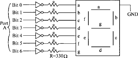
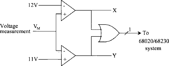
| 9.15 | In Figure P9.15, if VM > 12 V, turn an LED ON connected at bit 3 of port A. If VM < 11 V, turn the LED OFF. Using ports, registers, and memory locations as needed and level 1 autovectored interrupt:
(a) Draw a neat block diagram showing a 68020/68230 microcomputer and the connections in Figure P9.15 to 68230 ports. (b) Write the main program and the service routine in 68020 assembly language. The main program will initialize ports and wait for interrupt. The service routine will accomplish the task and stop.
|