10
ASSEMBLY LANGUAGE PROGRAMMING WITH THE PENTIUM: PART 1
In this chapter we describe the fundamental concepts associated with assembly language programming with the Intel Pentium microprocessor. The first part of the Pentium's instruction set is introduced in this chapter. Topics include Pentium registers, addressing modes, and data transfer and arithmetic instructions. Several examples of assembly language programming using these instructions are provided.
Note that the Pentium contains 32 address pins and hence can directly address 232 or 4 Gigabytes (GB) of memory. This large addressing space allows the Pentium to perform many operating system features, such as multitasking. The Pentium operates in two modes of operation: real mode and protected mode.
The real mode appears to programmers as a fast 8086 with a few new instructions. Like the 8086, the Pentium can directly address a maximum of one Megabyte (MB) of main memory. Since DOS is a real mode operating system, a Pentium-based PC that boots up into DOS operates in real mode. The real mode is the mode of operation of the Pentium upon hardware reset.
While in the real mode, the protected mode can be selected via execution of a single instruction. With a large directly addressable memory in protected mode, the Pentium provides support for multitasking, virtual memory addressing, memory management and protection, and control over instruction and data cache. Microsoft took advantage of these features and designed the Windows operating system to run in protected mode.
To write programs in the protected mode, a background in operating systems theory is required. Hence, real mode operation is emphasized in this book to present programming concepts with the Pentium in a very simplified manner. Note that real mode operation of the Pentium is widely used in many industrial applications.
The Pentium uses segmented memory in both real mode and, protected mode utilizing segmentation. This means that each address used by the programmer (also called “logical address”) consists of two components. In real mode, these components are a 16-bit segment and a 16-bit offset. The Pentium translates these two 16-bit components for each logical address into a 20-bit physical address using on-chip hardware. In protected mode, the Pentium uses 32-bit physical addresses, and the technique of translating each logical address into a 32-bit physical address is quite different than real mode. Note that the Pentium provides a special mechanism to use 32-bit offsets in real mode. Hence, both 16- and 32-bit offsets can be used in real mode.
10.1 Introduction
The Intel Pentium is a 32-bit microprocessor based on their 80486. The 80486, on the other hand, is an enhanced 80386. Hence, before proceeding further, an overview of the basic features of the 80386 and 80486 will be helpful. The Intel 80386 was Intel's first 32-bit microprogrammed microprocessor. Its introduction in 1985 facilitated the introduction of Microsoft's Windows operating systems. The high-speed computer requirement of the graphical interface of Windows operating systems was supplied by the 80386. Also, the on-chip memory management of the 80386 allowed memory to be allocated and managed by the operating system. In the past, memory management was performed by software.
The 80386 is based on Intel's 16-bit microprocessor, the 8086. The 80386 is software compatible with the 8086 at the object code level. The 80386 includes eight 32-bit general-purpose registers. The processor can handle 8-, 16-, and 32-bit data types. It has separate 32-bit data and 32-bit address pins, and generates a 32-bit physical address. The 80386 can address directly up to 4 GB (232) of physical memory. The 80386 can be interfaced to external cache memory. The chip has 132 pins and is typically housed in a pin grid array (PGA) package. The 80386 is designed using high-speed HCMOS III technology.
The 80386 is pipelined and can perform instruction fetching, decoding, execution, and memory management functions in parallel. The on-chip memory management and protection hardware translates logical addresses to physical addresses and provides the protection rules required in a multitasking environment. The 80386 contains a total of 129 instructions. The 80386 protection mechanism, paging, and instructions to support them are not present in the 8086.
The main differences between the 8086 and the 80386 are that the 80386 contains 32-bit addresses and data types and paging and memory management. To provide these features and other applications, several new instructions are added in the 80386 instruction set beyond those of the 8086.
TABLE 10.1 Basic Differences Between the 80486 and Original Pentium Microprocessors

Like the 80386, the 80486, introduced in 1989, is a 32-bit microprocessor. It executes the complete instruction sets of the 80386 and the 80387DX floating-point coprocessor. Unlike the 80386, the 80486 on-chip floating-point hardware eliminates the need for an external floating-point coprocessor chip, and the on-chip cache minimizes the need for an external cache and associated control logic.
The 80486 is object code compatible with the 8086 and 80386 microprocessors. Like the 80386, the 80486 contains separate 32-bit address and 32-bit data pins.
The 80486 has an internal 8-kB cache memory. This provides fast access to recently used instructions and data. The internal write-through cache can hold 8 kB of data or instructions. The on-chip floating-point unit performs floating-point operations on the 32-, 64-, and 80- bit arithmetic formats specified in the IEEE standard. The fetching, decoding, execution, and address translation of instructions are overlapped within the 80486 processor using instruction pipelining. This allows a continuous execution rate of one clock cycle per instruction for most instructions. Hence, the 80486 is a scalar microprocessor.
The original Pentium was introduced in 1993. Intel could not name it the 80586 because of problems with trademarking the numbers. The Pentium is very similar to the 80486 except that it has a 64-bit data bus. The Pentium contains two independent pipelines and has the capability of executing two instructions per cycle. Hence, the Pentium is a superscalar microprocessor.
Table 10.1 summarizes the fundamental differences between the basic features of the 80486 and the original Pentium. Like its predecessor, the 80486, the Pentium is 100% object code compatible with 8086/80386 systems. BICMOS (Bipolar and CMOS) technology is used for the Pentium.
In December 1994, Intel detected a flaw in the Pentium chip while performing certain division calculations. The Pentium is not the first chip that Intel has had problems with. The first version of the Intel 80386 had a math flaw that Intel fixed before there were any complaints. Some experts feel that Intel should have acknowledged the math problem in the Pentium when it was first discovered and then offered to replace the chips. In that case, the problem with the Pentium probably would have been ignored by users. However, Intel was heavily criticized by computer magazines when the division flaw in the Pentium chip was detected.
The flaw in the division algorithm in the Pentium was caused by a problem with a look-up table used in the division. Errors occur in the fourth through the fifteenth significant decimal digits. This means that in a result such as 5.78346, the last three digits could be incorrect. For example, the correct answer for the operation 4,195,835 − (4,195,835 + 3,145,727) + (3,145,727) is zero. The Pentium provided the wrong answer: 256. IBM claimed that this problem can occur once every 24 days. Intel eventually fixed the division flaw in the Pentium.
The Pentium microprocessor contains the complete 80486 instruction set along with some new ones that are discussed later. Pentium's on-chip memory management unit is completely compatible with that of the 80486.
Pentium's on-chip floating-point hardware has been redesigned completely over the 80486. Faster algorithms provide up to ten fold speed-up for common operations such as add, multiply, and load. The two instruction pipelines and on-chip floating-point unit are capable of independent operations. Each pipeline issues frequently used instructions in a single clock cycle. The dual pipelines can jointly issue two integer instructions in one clock cycle or one floating-point instruction (under certain circumstances, two floating-point instructions) in one clock cycle.
Branch prediction is implemented in the Pentium by using two prefetch buffers, one to prefetch code in a linear fashion and one to prefetch code according to the contents of the branch target buffer (BTB), so the code required is almost always prefetched before it is needed for execution. Note that the branch addresses are stored in the BTB.
There are two instruction pipelines, the U-pipe and the V-pipe, which are not equivalent and interchangeable. The U-pipe can execute all integer and floating-point instructions, whereas the V-pipe can execute only simple integer instructions and floating-point exchange register contents (FXCH) instructions. The instruction decode unit decodes the prefetched instructions so that the Pentium can execute them. The control ROM includes the microcode for the Pentium processor and has direct control over both pipelines. A barrel shifter is included in the chip for fast shift operations.
10.2 Pentium Registers
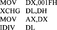
Figures 10.1(a) and 10.1(b) show the Pentium registers. The Pentium contains 8-, 16-, and 32-bit registers classified into four groups: general-purpose registers, stack pointers and index registers, extended instruction pointer and flag register, and Segment registers. These are described next.
10.2.1 General-Purpose Registers
As shown in Figure 10.1(a), the Pentium has four 32-bit general-purpose registers: EAX, EBX, ECX, and EDX. These registers can be used for arithmetic, logic, and other operations as follows:
- EAX, EBX, ECX, and EDX as four 32-bit registers
- AX (low 16 bits of EAX), BX (low 16 bits of EBX), CX (low 16 bits of ECX), and DX (low 16 bits of EDX) as four 16-bit registers
- AH, AL, BH, BL, CH, CL, DH, and DL as eight 8-bit registers
Some general-purpose registers perform specific functions for certain instructions as follows:
- The uses of EAX, AX, and AL registers are assumed by some instructions. The I/O (IN or OUT) instructions always use the EAX, AX, or AL for inputting or outputting 32-, 16- or 8-bit data from or to an I/O port. Multiplication and division instructions also use the EAX, AX, or AL.
- The ECX or CX register is known as the counter register respectively in protected mode and real mode because some instructions use these registers for a loop count for iterative instructions.
- The EDX or DX register is used during multiplication and division instructions. EDX is used by 32 × 32 multiplication and 64 ÷ 32 instructions. DX, on the other hand, is used by 16 × 16 multiplication and 32 ÷ 16 division instructions.
Note that BX can be used as a 16-bit pointer to memory while EAX, EBX, ECX, and EDX can be used as 32-bit pointers to memory.
10.2.2 Stack Pointers and Index Registers
The Pentium stack pointer registers can be used as 32-bit or 16-bit registers as follows:
- ESP and EBP as 32-bit system stack pointer and 32-bit user stack pointer respectively in protected mode
- SP and BP as 16-bit system stack pointer and 16-bit user stack pointer respectively in real mode (the stack pointer registers are typically used for stack operations)
The Pentium index registers can be used as 32- or 16-bit registers as follows:
- ESI and EDI as 32-bit registers
- SI and DI as 16-bit registers [the index registers (SI, DI, ESI, EDI) can also be used as general-purpose registers or memory pointers or by string instructions]
10.2.3 Extended Instruction Pointer and Flag Register
The extended instruction pointer (EIP) contains the offset address relative to the start of the current code segment of the next sequential instruction to be executed in protected mode. The low-order 16 bits of EIP is named IP and is useful when the Pentium executes instructions in real mode. The flag register is a 32-bit register, named EFLAGS is shown in Figure 10.1(b). The low-order 16 bits of EFLAGS is named FLAGS. The Pentium flags in the EFLAGS register are grouped into three types: status flags, control flags, and system flags. In the real mode, the status flags and control flags are used. The system flags along with status and control flags are used in the protected mode.
The status flags include CF, PF, AF, ZF, SF, and OF.
- AF (the auxiliary carry flag) is set to 1 if there is a carry due to addition of the low 4 bits into the high 4 bits or a borrow due to the subtraction of the low 4 bits from the high 4 bits of a number; otherwise, AF = 0. This flag is used by BCD arithmetic instructions.
- CF (the carry flag) is set to 1 if there is a carry from addition or a borrow from subtraction; otherwise, CF = 0.
- OF (the overflow flag) is set to 1 if there is an arithmetic overflow (i.e., if the size of the result exceeds the capacity of the destination location); otherwise, OF = 0. Note that overflow, OF = Cf
 Cp where Cf is the final carry and Cp is the previous carry. An interrupt on overflow instruction is available to generate an interrupt indicating the occurrence of an overflow.
 - SF (the sign flag) is set to 1 if the most significant bit of the result is 1 indicating a negative number; SF = 0 if the most significant bit of the result is 0 indicating a positive number.
- PF (the parity flag) is set to 1 if the result has even parity; PF = 0 when the result has odd parity.
- ZF (the zero flag) is set to 1 if the result is zero; ZF = 0 for a nonzero result.
The Pentium has 3 control bits in the flag register that can be set or cleared by the programmer:
- Setting DF (the direction flag) to 1 causes string instructions to auto decrement; clearing DF to 0 causes string instructions to autoincrement.
- Setting IF (the interrupt flag) to 1 causes the Pentium to recognize external mask able interrupts; clearing IF to 0 disables these interrupts.
- Setting TF (the trap flag) to 1 places the Pentium in the single-step mode. In this mode, the Pentium generates an internal interrupt after execution of each instruction. The user can write a service routine at the interrupt address vector to display the contents of desired registers and memory locations. The user can thus debug a program.
The system flags control I/O, mask able interrupts, debugging, task switching, and enabling of virtual 8086 execution in a protected, multitasking environment.
- IOPL (I/O privilege level) is a 2-bit field that supports the Pentium protection feature.
- NT (nested task) controls the IRE operation. If NT = 0, a usual return from interrupt is taken by the Pentium by popping FLAGS, CS, and EPIC from the stack. If NT = 1, the Pentium returns from an interrupt via task switching.
- RF (resume flag) is used during debugging.
- VM (virtual 8086 mode): when the VIM bit is set to 1, the Pentium executes 8086 programs. When the VIM bit is 0, the Pentium operates in protected mode.
- AC (alignment check): When the AC bit is set to 1, the Pentium operates in alignment check mode and generates exceptions when reference is made to an unaligned memory address.
- VIF (virtual interrupt flag) is a copy of the interrupt flag bit.
- VIP (virtual interrupt pending) is used in multitasking to provide the operating system with virtual interrupt flags and interrupt pending information.
- ID (identification) gives the ability to set and clear the ID flag. It indicates that the processor supports the CPUID instruction. The CPUID instruction provides information to the software about the Pentium microprocessor, such as its version number and manufacturer.
10.2.4 Segment Registers
The six 16-bit segment registers (CS, SS, DS, ES, FS, and GS) generate memory addresses when combined with certain registers in the Pentium. These registers support the segmented memory mechanism of the Pentium. In this mechanism, memory is divided into segments in which each segment is a small section of the memory. The Pentium, at any time, can point to six segments of the main memory.
A program contains instructions and data. The Pentium uses segmented memory to store instructions in a code segment and the data portion of the program in a data segment. The CS register points to the code segment while the DS register points to the data segment. The SS register points to the stack segment. The three other data segment registers, ES, FS, and GS, are used in a similar manner as the DS register. These registers can be used if the program needs additional memory for storing data.
A segment register works differently in the real and protected modes of operation. Let us discuss them in the following.
10.3 Modes of Operation
The Pentium has two primary processing modes: real and protected. In addition, the Pentium microprocessor is provided with a system management mode (SMM), which allows one to design for low power usage. SMM is entered through activation of an external interrupt pin (system management interrupt, SMI#). Real mode is the mode of operation of the processor upon hardware reset. This mode appears to programmers as a fast 8086 with a few new instructions. The architecture of the Pentium processor in the real mode is identical to that of the 8086 microprocessor. Protected mode is the normal 32-bit application of the Pentium. All instructions and features of the Pentium are available in this mode only. While in protected mode, the pentium can execute “real address” mode instructions directly in a protected, multitasking environment using a feature called the Virtual 8086 mode (also called V86 mode). Virtual 8086 is not really a Pentium mode, but an attribute that can be enabled for any task with appropriate software while in protected mode. This feature allows the Pentium to go back and forth repeatedly between the protected and V86 modes at a fast speed. When entering into V86 mode, the Pentium can execute an 8086 program. The processor can then leave V86 mode and enter the protected mode to execute a Pentium program.
As mentioned before, the Pentium enters the real mode upon hardware reset. The Pentium contains a control register called CR0 to facilitate mode switching. In the real mode, the protection enable (PE) bit at bit 0 in the 32-bit control register, CR0 is cleared to zero. Setting the bit 0 in control register, CR0 (PE bit) by executing a MOV instruction such as MOV CR0,reg32 will place the Pentium in protected mode. Note that reg32 can be one of the Pentium's 32-bit general-purpose registers, such as EAX. Also, data cannot be moved into CR0 using the immediate mode. When the Pentium is in protected mode, setting the VIM (virtual mode) bit in the flag register (the FLAGS register) places the Pentium in the V86 mode. The real and protected modes of the Pentium are described in more detail below.
10.3.1 Real Mode
The real mode is provided with the Pentium to run programs for the 8086. In real mode operation, the Pentium can address a maximum of 1 MB of the main memory directly using a 20-bit physical address. This means that the starting physical address is 00000H and the last addressable physical address is FFFFFH. In this mode, the Pentium uses a segmented memory. Two components, a segment value and an offset value, are required to specify a memory location (referred to as a logical address) in segmented memory organization. The programmer uses the logical addresses. The Pentium's on-chip hardware translates a logical address to its corresponding 20-bit physical address by shifting the contents of the segment register four times to the left, and then adding the 16-bit offset to it. There are some advantages to working with the segmented memory. First, after initializing the 16-bit segment registers, the Pentium has to deal only with offsets. That is, the Pentium has to manipulate and store 16- and 32-bit offsets. Second, because of memory segmentation, the Pentium can be used effectively in time-shared systems. For example, in a time-shared system, several users may share one Pentium. Suppose that the Pentium works with one user's program for, say, 5 ms. After spending 5 ms with one of the other users, the Pentium returns to execute the first user's program. Each time the Pentium switches from one user's program to the next, it must execute a new section of code and new sections of data. Segmentation makes it easy to switch from one user program to another.
In real mode, the Pentium's main memory can be divided into 16 segments of 64 kB each (16 × 64 kB = 1 MB). A segment may contain codes or data. The Pentium uses 16-bit registers to address segments. For example, to address codes, the code segment (CS) register must be initialized in some manner (to be discussed later). A 16-bit Pentium register called the instruction pointer (IP), which is similar to the program counter of a typical microprocessor, addresses each location in a code segment linearly. Because the size of the IP is 16 bits, the segment size is 64 kB (216). Similarly, a 16-bit data segment register (DS, ES, FS,or GS) must be initialized to hold the segment value of a data segment. The contents of certain 16-bit registers are designed to hold a 16-bit offset in a 64-kB data segment. One of these address registers can be used to address each location linearly once the data segment is initialized by an instruction.
To access the stack segment in real mode, the Pentium's 16-bit stack segment (SS) register must be initialized; the 64-kB stack is addressed linearly by a 16-bit stack pointer (SP) register. Note that the stack memory must be a read/write (RAM) memory. Whenever the programmer reads from or writes to the Pentium stack, two components of a memory address must be considered: a segment value and an offset value. The SS register points to the current stack. The 20-bit physical stack address is calculated from the SS and SP for stack instructions such as PUSH and POP. The programmer can create a programmer's stack with the BP (base pointer) instead of the SP for accessing the stack using the based addressing mode. In this case, the 20-bit physical stack address is calculated from BP and SS.
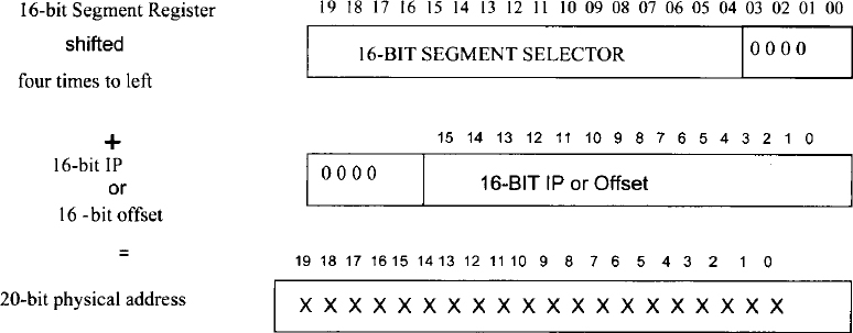
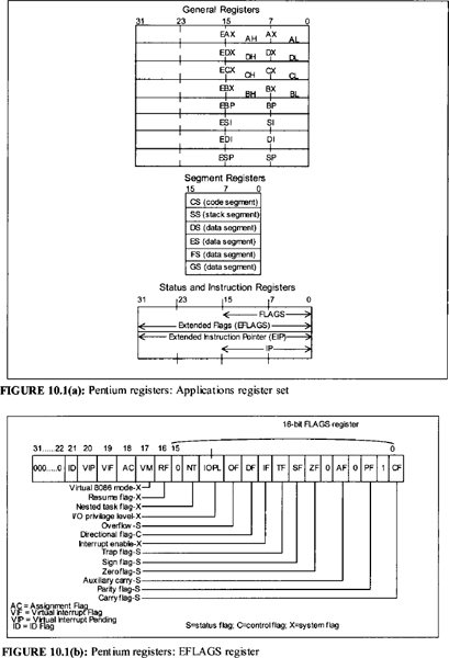
FIGURE 10.2 Pentium address translation in real mode.
The Pentium assembly language program works with two components in real mode while accessing memory. These two 16-bit components (the contents of a 16-bit segment register and a 16-bit offset or IP) form a logical address. As mentioned before, the programmer writes programs using these logical addresses in assembly language programming. The Pentium logically shifts the contents of the 16-bit segment register four times to left, and then adds the 16-bit IP or 16-bit offset to obtain the 20-bit physical address in the real mode. This is depicted in Figure 10.2. Note that because of the possibility of a carry, the resulting linear address may have as many as 21 bits. However, the carry (bit 20) is discarded and 20 bits are used as the linear address.
As an example, consider a logical address with the 16-bit code segment (CS) register contents of 2050H and the 16-bit Pentium instruction pointer (IP) containing a value of 0004H. When the Pentium executes this program and encounters the logical address, it will generate the 20-bit physical address as follows: Since the 16-bit contents of IP = 0004H, the 16-bit contents of code segment = 2050H, and the 16-bit contents of code segment value after shifting logically four times to the left = 20500H, the 20-bit physical address generated by the Pentium on the address bus is 20504H.
The segments can be contiguous, partially overlapped, fully overlapped, or disjointed. An example of how five segments (0 through 4), may be stored in physical memory is shown in Figure 10.3. In this example, segments 0 and 1 are contiguous (adjacent), 1 and 2 are partially overlapped, 2 and 3 are fully overlapped, and 2 and 4 are disjointed.
FIGURE 10.3 Example of Pentium memory segments.
Every segment must start on 16-byte memory boundaries. Typical examples of values of segments should then be selected based on physical addresses starting at 0000016, 0001016, 0002016, 0003016, …, FFFF016. A physical memory location may be mapped into (contained in) one or more logical segments. For example, consider a physical address 32040H. This address can be mapped as offset 2040H in segment 3000H or as offset 2000H in segment 3004H. Note that many applications can be written simply to initialize the segment registers and then forget them.
A segment can be pointed to by more than one segment register. For example, the DS and ES may point to the same segment in memory if a string located in that segment is used as a source segment in one string instruction and a destination segment in another string instruction. Note that for string instructions, a destination segment must be pointed to by the ES. One example of six currently addressable segments is shown in Figure 10.4.
In summary, the Pentium has six segment registers: CS, SS, DS, ES, FS, and GS. The four data segment registers (DS, ES, FS, and GS) can access four separate data segments. In the real mode, some examples of the default segment registers with the corresponding 16-bit offsets or values shown in Table 10.2 are shown.
In real mode, the Pentium obtains the 20-bit physical address as follows:
- For instructions: 16-bit segment register, CS and 16-bit offset in IP.

FIGURE 10.4 Six currently addressable Pentium segments.
TABLE 10.2 Some Examples of Registers and Offsets in Real Mode
Segment Register 16-bit Offset CS IP DS BX, SI, DI, 16-bit value SS SP or BP - For data: 16-bit segment register, DS and 16-bit offset in BX, SI, DI, or an offset value.
- For system stack: 16-bit segment register, SS and 16-bit offset in SP.
- For user stack: 16-bit segment register, SS and 16-bit offset in BP.

10.3.2 Protected Mode
In the protected mode, the Pentium uses 32-bit addresses. In this mode the Pentium supports both segmentation and paging. Paging is useful for implementing virtual memory. Note that paging is transparent to the application program, whereas segmentation is not. Pentium's paging feature will not be described here. Rather, a brief overview of the protected mode segmented memory architecture is provided.
In the proteced mode, Pentium's on-chip segment translation hardware translates a logical address into a 32-bit linear address. The mechanism of generating physical addresses in the protected mode is quite different from that of the real mode. As mentioned before, in real mode, the Pentium generates 20-bit physical addresses by shifting 16-bit segment registers four times to the left, and then adding to a 16-bit offset.
Accessing a large memory of 4 GB in the protected mode requires a change of segment plus offset addressing technique used in the real mode. While accessing memory in the protected mode, the Pentium still uses offset to obtain information in a memory segment. However, it does not use the segment register directly. Instead, the contents of the segment register are used as an index (upper 13 bits of the selector) to a table. Hence, during the segment translation process, the contents of the segment register are used as an index into a segment descriptor table to obtain a descriptor. Segment descriptors contain the 32-bit segment base address, its size, and access rights. The Pentium adds a 16- or 32-bit offset to the 32-bit base address to translate a logical address to its corresponding linear address. This is depicted in Figure 10.5. The on-chip paging translation hardware then translates the linear address into a 32-bit physical address. If no paging is used, the linear address is the same as the physical address. In the protected mode, some examples of the default segment registers with the corresponding 32-bit offsets or values shown in Table 10.3 are shown.
TABLE 10.3 Some Examples of Registers and Offsets in Protected Mode
| Segment Register | 32-bit Offset |
| CS | EIP |
| DS | EAX, EBX, ECX, EDX, ESI, EDI, an offset value |
| SS | ESP or EBP |
10.4 Pentium data Organization
The Pentium microprocessor contains instructions that can operate on various types of data. These data types include bit, byte, 16-bit word, and 32-bit doubleword. Shift and rotate instructions typically operate on bits. Bytes are stored in Pentium's 8-bit registers such as AH, AL, BH, BL,CH, CL, DH, and DL. Word data types are stored in Pentium's 16-bit registers AX, BX, CX, DX, SI, DI, and BP. Also, each of the 16-bit registers AX, BX, CX, and DX can hold 2 bytes. For example, 8-bit registers AH and AL will contain 23H (the upper byte) and 45H (the lower byte) of the 16-bit data 2345H stored in the 16-bit register AX. Doubleword (32-bit) data types are normally stored in 32-bit registers such as EAX, EBX, ECX, EDX, ESI, EDI, and EBP.
The memory of a Pentium-based microcomputer is organized as bytes. In the real mode, each byte is addressed uniquely with 20-bit addresses of 0000016, 0000116, …,FFFFF16. A Pentium word in memory consists of any two consecutive bytes; the low-addressed byte is the low byte of the word, and the high-addressed byte contains the high byte as follows:

The 16-bit word at the even address 0200016 is A10216. Next, consider a word stored at address 3015116 as follows:

The 16-bit word stored at the odd address 3015116 is 462E16.
The Pentium assigns the low address to the low byte of a 16-bit register and the high address to the high byte of the 16-bit register for 16-bit transfers between the Pentium and main memory. This is called little-endian byte ordering. In contrast, Motorola microprocessors such as the 68020 use big-endian byte ordering,, in which the 68020 assigns the high address to the low byte of a 16-bit register and the low address to the high byte of the 16-bit register for 16-bit transfers between the 68020 and main memory.
10.5 Assembly Language Programming with the Pentium
The assembly language program is translated into binary via a program called an assembler. The assembler program reads each assembly instruction of a program as ASCII characters and translates them into the respective binary op-codes. For example, the Pentium assembler translates the HLT instruction into its binary op-code is 1111 0100 (F4 in hex) as depicted in Table 10.4.
TABLE 10.4 Conversion of HLT into Its Binary Op-Code

An advantage of the assembler is address computation. Most programs use addresses within the program as data storage or as targets for jumps or calls. When programming in machine language, these addresses must be calculated by hand. The assembler solves this problem by allowing the programmer to assign a symbol to an address. The programmer may then reference that address elsewhere by using the symbol. The assembler computes the actual address for the programmer and fills it in automatically. One can obtain hands-on experience with a typical assembler for a microprocessor by downloading it from the Internet.
As mentioned in Chapter 5, each line in an assembly language program includes four fields:
- Label field
- mnemonic or op-code field
- Operand field
- Comment field
The assembler ignores the comment field but translates the other fields. The label field must start with an uppercase alphabetic character.
The assembler must know where one field starts and another ends. Most assemblers allow the programmer to use a special symbol or delimiter to indicate the beginning or end of each field. Typical delimiters used are spaces, commas, semicolons, and colons:
- Spaces are used between fields.
- Commas (,) are used between addresses in an operand field.
- A semicolon (;) is used before a comment.
- A colon (:) is used after a label.
To handle numbers, most assemblers including the Pentium assembler, consider all numbers as decimal numbers unless specified. Most assemblers will also allow binary, octal, or hexadecimal numbers. The user must define in some way the type of number system used. This is generally done by using a letter following the number. Typical letters used are B for binary, Q for octal, and H for hexadecimal. Typical assemblers, such as the MASM32, require hexadecimal numbers to start with a digit (0 through 9). A 0 is typically used if the first digit of the hexadecimal number is a letter. This is done to distinguish between numbers and labels. For example, typical assemblers will normally require the number F3H to be represented as 0F3H; otherwise, the assembler will generate an error. Assemblers use pseudoinstructions or directives to make the formatting of the edited text easier. These directives are not translated directly into machine language instructions. Typical assembler directives are discussed in the following.
ORIGIN (ORG) The directive ORG lets the programmer place the programs anywhere in memory. Typical ORG statements are
![]()
Most assemblers assign a value of zero to starting address of a program if the programmer does not define this by means of an ORG.
Equate (EQU) The EQU assigns a value in its operand field to an address in its label field. This allows the user to assign a numerical value to a symbolic name. The user can then use the symbolic name in the program instead of its numerical value. Atypical example of EQU is START EQU 0200H, which assigns the value 0200H in hexadecimal to the label START.
Typical assemblers, such as the MASM32 (used to assemble Pentium programs in this book), require hexadecimal numbers to start with a digit. A 0 is used if the first digit of the hexadecimal number is a letter; otherwise, an error will be generated by the assembler. This is done to distinguish between numbers and labels. For example, TEST EQU 0A5H will assign A5 in hex to the label TEST.
Define Byte (DB) The directive DB is generally used to set a memory location to a certain byte value. For example,
![]()
will store the data value 45 hex to the address START. The DB directive can be used to generate a table of data as follows:
![]()
In this case, 20 hex is the first data of the memory location 7000; 30 hex, 40 hex, and 50 hex occupy the next three memory locations. Therefore, the data in memory will look like this:

Define Word (DW) The directive DW is typically used to assign a 16-bit value to two memory locations. For example,
![]()
will assign C2 to location 7000 and 4A to location 7001. It is assumed that the assembler will assign the low byte first (C2) and then the high byte (4A). The DW directive can be used to generate a table of 16-bit data as follows:
![]()
In this case, the three 16-bit values 5000H, 6000H, and 7000H are assigned to memory locations starting at the address 8000H. That is, the array would look like this:

Define Doubleword (DD) Similar to DB and DW, the directive DD is typically used to assign a 32-bit value to four memory locations. The directive DD can be used to create a table in memory containing 32-bit data.
END The directive END indicates the end of the assembly language source program.
.CODE The .CODE directive is used to indicate the start of a code segment.
.DATA The .DATA directive is used to indicate the start of a data segment.
.MODEL The .MODEL directive tells the assembler the type of program being created. Two examples of model types are SMALL and FLAT. SMALL programs contain one code segment and one data segment with 16-bit addressing. FLAT programs, on the other hand, contains one code segment and one data segment with 32-bit addressing. All Pentium assembly language programs in this book are either SMALL or FLAT. Also, STDCALL must be included with a model for inclusion of assembler's standard library routines required to assemble the programs.
To develop Pentium assembly language programs in this book, MASM32 assembler and OllyDebugger simulator are used. These programs are very user friendly, and can be downloaded from the Internet free of charge, using the following web sites.
- MASM32 http://www.assemblercode.com/masm32/m32v9r.zip
- OllyDebugger http://www.ollybg.de/odbg110.zip
The zip files for the MASM32 and OllyDebugger are provided in a CD. The CD also contains a tutorial showing a step-by-step procedure for installing, assembling, and debugging a typical Pentium assembly language program using the MASM32 and OllyDebugger. Most of the Pentium programming examples in this book are assembled using the MASM32 and debugged using OllyDebugger. Screen shots are provided on the CD verifying correct operation of all assembly language programs via simulations using test data.
As an example, a typical program for adding two 16-bit numbers written in Pentium assembly language is shown below.


The assembly language program above called a source file contains all instructions required to execute a program. The assembler converts the source file into an object file containing the binary codes or machine codes that the Pentium will understand. In typical assemblers, including the Pentium, the source file must be stored with a file extension called .ASM. Suppose that the programmer stores the source file above as SUM.ASM. To assemble the program, SUM.ASM is presented as input to the assembler. The assembler typically generates two files: SUM.OBJ and SUM.LST.
The SUM.OBJ is an object file, a binary file containing the machine code and data that correspond to the assembly language program in the source file (SUM.ASM). The object file includes additional information about relocation and external references. The object file is not normally ready for execution.
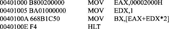
The SUM.LST, a list file, shows how the assembler interprets the source file. SUM.LST may be displayed on the screen. Suppose that the source file SUM.ASM is assembled at CS = 0040H, and IP = 1000H using the MASM32. The SUM.LST file is as follows:
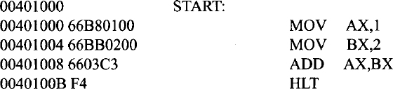
The first column gives the default CS and IP values where codes are stored. These values are generated automatically by the MASM32. For example, the machine code (66B80100H) for the first instruction, MOV AX,1 is stored in CS:IP = 0040H:1000H. Since this instruction takes 4 bytes, the machine code for the next instruction, MOV BX,2 starts at CS:IP = 0040H: 1004H. Note that the comment fields in the SUM.ASM file are not translated by the MASM32.
To develop a large program by a group of programmers, each programmer may write a portion of the whole program. The individual programs must be tested and assembled to ensure their proper operation. When all portions of the program are verified for correct operation, their object files must be combined into a single object program using a linker, a program that checks each object file and finds certain characteristics, such as the size in bytes and its proper location in the single object program. The linker also resolves any issues in regard to cross-references to labels. Also, a library of object files is typically used to reduce the size of the source file. The library files may contain frequently used subroutines and/or sections of codes. Rather than writing these codes repeatedly in the source file, a special pseudoinstruction is used to tell the assembler that the code must be inserted at the linking time by the linker. When linking is completed, the final object file is called an executable (.EXE) file. Finally, a program called the loader can be used to load the .EXE file in memory for execution.
10.6 Pentium Addressing Modes
Assembly language programs in Pentium typically contain two logical parts: data and code. The ways of specifying the locations of the operands are called addressing modes. Note that an operand may typically be immediate data, or data stored in a Pentium's register or in a data segment.
Several instruction types along with a number of addressing modes and data types, make the Pentium a very powerful microprocessor. For simplicity, most of the examples of addressing modes described below use the Pentium instruction MOV destination, source. This instruction transfers the contents of a source (register or a memory location) into a destination (register or a memory location).
Also, when a physical address is generated by the Pentium in the real mode, a 20-bit value appears on Pentium's low 20 of the total 32 address pins. Note that Pentium address pins A2 A1 A0 are encoded from the byte enable pins, BE7# through BE0#. As mentioned earlier, this 20-bit physical address is generated by the Pentium using two components (logical address) provided by the programmer. These components are a 16-bit segment value and a 16-bit offset value. The Pentium shifts the segment four times to left and then adds the offset to generate a 20-bit physical address.
When accessing a memory location, the programmer must provide a segment value and an offset value. Data transfer instructions such as MOV use the data segment register (DS) as default; the offset is provided by the contents of certain registers (mentioned before) or an offset value. For instructions, the 20-bit physical address is computed from CS and IP. For stack operations, SS and SP are used automatically to compute the physical address for the system stack.
The programmer can initialize the data segment registers (DS, ES, FS, GS) and the stack segment register (SS) using AX, BX, CX, or DX. For example, to initialize DS to 5000H, the following instruction sequence can be used:
![]()
These segment registers cannot be initialized with immediate data. Also, CS cannot be initialized via programming. CS is typically initialized upon hardware reset. Note that while accessing a memory location, initialization of a segment register is required for generation of the 20-bit physical address. This will ensure correct execution of a program.
10.6.1 Pentium's 32-Bit Addressing in Real Mode
Although the 32-bit offsets are designed for protected mode applications, 32-bit offsets can be used for real mode applications. In the real mode, these 32-bit offsets must fall within the 64-kB range (0000H-FFFFH) used within a segment. This means that the contents of a 32-bit register holding an offset must be between 00000000H and 0000FFFFH. The advantage is that an extended register may be used as a base register or an index register or both in the same instruction. However, the ESP register is the only one that may be used as a base register, and cannot be used as an index register.
Sixteen- and 32-bit addresses (offsets) and data can be mixed using two override prefixes:
![]()
In the real mode, the value of a 32-bit offset may not exceed 65,535 (64K). This means that the low 16-bit of a 32-bit register can be used to hold the 16-bit offset in real mode. Both 16- and 32-bit data and offsets can be used in real mode, as illustrated below by examples.
The Pentium assembler (MASM32) translates the following instruction with 32-bit data:
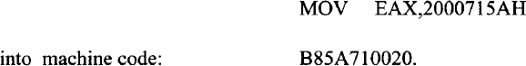
The Pentium assembler translates the following instruction with a 32-bit operand, ECX, and a 32-bit offset in EBX:
![]()
into machine code: 8B0B.
However, one can use 16-bit data and offsets for the Pentium assembler using the prefixes above as shown in the examples below.
The assembler translates the following instruction with a 16-bit operand, AX:
![]()
into machine code: 66B80200.
The Pentium assembler automatically inserts 66H (Operand size override prefix).
The assembler translates the following instruction with 16-bit operand CX:
![]()
into machine code: 668B0B.
The Pentium assembler automatically inserts 66H (operand size override prefix).
Next, Pentium assembler translates the instruction with 16-bit offset
MOV EAX, [BX]
into machine code: 678B07.
The Pentium assembler automatically inserts 67H (address size override prefix).
Note that both override prefixes can be mixed in an instruction as illustrated in the following. For example, the Pentium assembler translates the following instruction with a 16-bit offset and 16-bit operand:
![]()
into machine code: 67668B17
In this case, the Pentium assembler automatically inserts 6766 for address and operand override prefixes.
The Pentium provides various addressing modes to access instruction operands. Operands may be contained in registers, within the instruction op-code, in memory, or in I/O ports. The Pentium has 13 addressing modes, which can be classified into five groups:
- Register and immediate modes (two modes)
- Memory addressing modes (seven modes)
- Port addressing mode (two modes)
- Relative addressing mode (one mode)
- Implied addressing mode (one mode)
The addressing modes are illustrated utilizing Pentium instructions with directives of a typical assembler. Note that in the following, parentheses, ( ) are used to indicate the contents of a Pentium register or a memory location.
10.6.2 Register and Immediate Modes
Register Mode. In register mode, source operand, destination operand, or both may be contained in Pentium's 8-, 16-, or 32-bit registers. For example, MOV EAX,EBX moves the 32-bit contents of EBX into EAX, MOV AX,BX moves the 16-bit contents of BX into AX, and MOV AH,BL moves the 8-bit contents of BL into AH. In these examples, both operands are in register mode.
TABLE 10.5 Memory Addressing Modes for 16-bit Offset
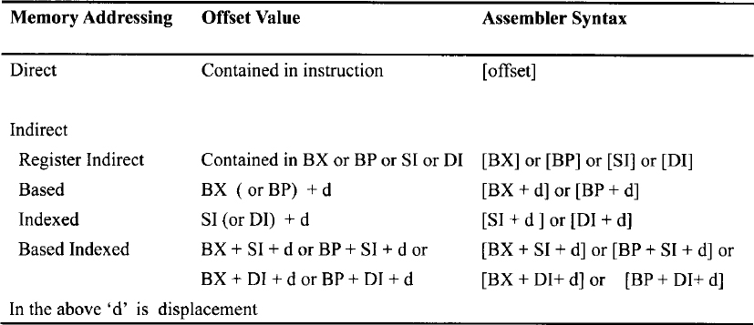
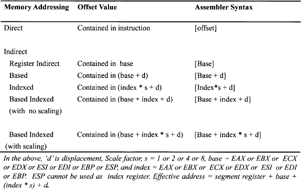
TABLE 10.6 Memory Addressing Modes for 32-Bit Offset
Immediate Mode. In the immediate mode, 8-, 16-, or 32-bit data can be specified as part of the instruction. For example, MOV ECX,2A715062H moves the 32-bit data 2A715062H into register ECX. Similarly, MOV DX, 4C00H moves the 16-bit data 4C00H into register DX. On the other hand, MOV BH, 2DH moves 8-bit data 2DH into register BH.
10.6.3 Memory Addressing Mode
The Pentium provides several addressing modes while accessing data in memory. Note that the programmer must specify a logical address to identify a memory location. Recall that the logical address contains two components: a segment value and an offset value. Memory addressing modes vary in how they specify the offset.
The memory addressing modes available for 16-bit offsets are the same as for the 8086. Tables 10.5 and 10.6 list the memory addressing modes for 16-bit and 32-bit offsets, respectively. Note that for memory indirect addressing with 32-bit offset (Table 10.6), the offset within the segment selected is the sum of maximum four components: a displacement, a base register, an index register, and a scaling factor of 1, 2, 4, or 8. The offset that results from adding these components is called an effective address. Note that all general purpose registers can be used as index registers. ESP cannot be used as an index register.
The various memory addressing modes are described below. Note that the numerical valuesare chosen arbitrarily for illustrative purposes.
Memory Direct Addressing. The direct addressing mode includes the offset directly in the instruction. A typical Pentium instruction such as the MOV transfers data between an 8-bit register such as AL, or a 16-bit register such as BX, or a 32-bit register such as EDX, and an offset located in the data segment. Memory-to-memory transfers are not allowed.
For example, MOV [2000H],AL, in real mode, transfers 8-bit contents of AL into a 20-bit physical address computed from the segment register DS and offset 2000H. Typical assemblers use square brackets around the offset 2000H to indicate that the contents of the memory location are at an offset 2000H from the segment DS.
Next, consider MOV BX, [5000H] in real mode. This instruction moves the contents of a 20-bit physical address computed from the segment register DS and offset 5000H to BX.
Finally, consider MOV [3000H], ECX in real mode. If (DS) = 2000H, (ECX) = 12345678H, (23000H) = 01H, (23001H) = 02H, (23002H) = 03H, and (23003H) = 04H, then after execution of MOV [3000H],ECX, the byte contents of four 20-bit physical addresses will be [23000H] = 78H, [23001H] = 56H, [23002H] = 34H, and [23003H] = 12H.
Register Indirect Addressing. In the register indirect mode, the offset is contained in one of the 16- or 32-bit general-purpose registers. The offset of a memory operand may be taken directly from one of the base or index 16-bit registers (BX, BP, SI, DI) or 32-bit registers (EAX, EBX, ECX, EDX,ESI, EDI, EBP). Note that 16-bit registers AX, CX, DX, and SP and the 32-bit register ESP cannot be used indirectly to hold 16-bit or 32-bit offset, respectively.
Next, consider MOV CX,[BX] in real mode. If prior to execution of the instruction, (DS) = 2000H, (BX) = 0004H, and (20004H) = 24H, (20005H) = 02H, then, after execution of MOV CX,[BX], the contents of CH and CL are 02H and 24H respectively. Note that the segment register used in MOV CX,[BX] can be overridden, such as MOV CX,ES:[BX], Now, the MOV instruction will use ES instead of DS. If prior to execution of MOV CX,ES:[BX], (BX) = 0004H, (ES) = 1000H, and (10004H) = 02H, (10005H) = 00H, then after MOV CX,ES:[BX], the register CX will contain 0002H.
Typical examples of indirect addressing using 32-bit registers for offset include MOV DX,[ECX] and MOV [EAX],EBX. Next, consider as an example MOV AX,[EDX] in real mode. Note that in real mode, the contents of EDX can have a value between 00000000H and 0000FFFFH. If prior to execution of this instruction, (AX) = F092H, (EDX) = 00002000H, (DS) = 3000H, (32000H) = 20H, and (32001H) = 30H, then after execution of MOV AX,[EDX], the 16-bit register AX will contain 16-bit data 3020H; (AH) = 30H, (AL) = 20H. Note that all numerical values in the above are chosen arbitrarily for illustrative purposes.
For register indirect addressing mode using BX, DI, or SI to contain the 16-bit offset, the DS register is used as the segment register by default. The SS register is used as a default segment register if BP is used indirectly to hold the 16-bit offset. For a 32-bit offset, the DS is used by default as the segment register if EAX, EBX, ECX, EDX, ESI, or EDI is used to hold the 32-bit offset; SS is used as a default segment register if EBP is used to hold the 32-bit offset.
Note that in the real address mode the contents of the 32-bit register holding the offset must be between 00000000H and 0000FFFFH.
The size of the data is typically specified by the register size when one of the operands is a register. For example, MOV BH, [SI] in the real mode transfers the 8-bit contents of a 20-bit physical address computed from 16-bit offset in SI and the segment register DS into BH. Note that in this case, the 8-bit register specifies the 8-bit data size. However, there are certain instances in which the size of the data needs to be specified by assembler directives BYTE PTR, WORD PTR, or DWORD PTR. For example, MOV BYTE PTR [BX], 5OH defines the location addressed by offset in BX and the segment register, DS as a byte. The instruction, MOV WORD PTR [BX],5 in the real mode will treat the location addressed by the 20-bit physical address computed from BX and DS as 16-bit. This means that this instruction will convert decimal number 5 into 16-bit as 0000000000000101 in binary, and then transfer this data into 16-bit memory. Similarly, MOV DWORD PTR [SI],70 specifies the memory location as 32-bit.
Based Addressing. For 16-bit offset, the effective address is the sum of a displacement value (0 or signed 8-bit or signed 16-bit) and the contents of register BX or BP. The signed 8-bit displacement gives a range of −12810 to +12710, with 0 being positive. The signed 16-bit, on the other hand, provides a range of −3276810 to + 3276710, with 0 being positive. Note that if the displacement is 8-bit, and the register is 16-bit, the displacement is sign-extended to 16 bits before adding it to the 16-bit register. Typical example includes MOV [BX + 3], AL.
Assume real mode. If prior to execution of this instruction, (BX) = 0200H, (DS) = 5000H, (50203H) = A2H, and (AL) = 05H, then after execution of this instruction, the contents of 20-bit physical address 50203H will be 05H. Note that a typical assembler uses either MOV [BX+3], AL or MOV 3 [BX],AL.
For a 32-bit offset, the effective address is the sum of a displacement value (0 or signed 8-bit or signed 32-bit) and the contents of a base register. A typical example include MOV [ECX + 8], EDX. Assume the real mode. Note that ECX + 8 in real mode can have a maximum value of 0000FFFFH. If prior to execution of this instruction, (ECX) = 00000200H, (DS) = 3000H, (30208H) = A2H, (30209H) = 05H, (3020AH) = 06H, (3020BH) = 02H, and (EDX) = 0102F305H, then after execution of this instruction, the contents of the four affected 20-bit physical addresses will be as follows: (30208H) = 05H, (30209H) = F3H, (3020AH) = 02H, and (3020BH) = 01H. If the displacement is 8-bit, and the register is 32-bit, the displacement is sign-extended to 32 bits before adding it to the 32-bit register.
Next, consider MOV AX,[BX+4] in real mode. This instruction moves the contents of the 20-bit physical address computed from a segment register and BX + 4 into AX. The segment register is DS (when the content of BX is used as offset), or SS (when the content of BP is used as offset). The content of BX is unchanged. The displacement (4 in this case) can be unsigned 16-bit or signed 8-bit. This means that if the displacement is 8-bit, the Pentium sign-extends this to 16-bit. Segment register SS is used when the stack is accessed; otherwise, this mode uses segment register DS. When memory is accessed, the 20-bit physical address is computed from BX and DS. On the other hand, when the stack is accessed, the 20-bit physical address is computed from BP and SS. Note that BP may be considered as the user stack pointer while SP is the system stack pointer. This is because SP is used automatically by some Pentium instructions (such as the CALL subroutine).

FIGURE 10.6 Uses of based addressing mode.
Based addressing mode is useful when one wants to access the same record type among several occurrences in a data structure which may be stored at different places in memory. For example, consider Figure 10.6(a). In the figure, personal records of N employees are stored starting at an offset 2000H. Assume that each record type is 8 bits wide. For example, the element “salary” of the employee with NAME 0 can be loaded into an 8-bit register such as AL of the Pentium using the instruction MOV AL, [ALPHA + BX], where ALPHA is the 8-bit displacement 02H and BX contains the starting address of RECORD 0. Now, to access the salary of RECORD N, the programmer simply changes the contents of BX to 3000H.
The based addressing mode with BP is also a very convenient way to access stack data in the real mode, as shown in Figure 10.6(b). BP can be used as a stack pointer in SS to access local variables. Consider the following instruction sequence (chosen arbitrarily to illustrate the use of BP for stack):

This mode can also be used to access an element in an array. Assume the real mode. Assume that an array of 50 bytes is stored in memory at an offset 3000H in DS. Note that the first element in the array is element 0 and the last element is element 49. Now, to access, say, element 4 in the array, register BX can be initialized with offset 3000H and the instruction MOV CL,[BX + 4] can be executed to read element 4 from the array into CL.
Indexed Addressing. In this mode, the 16-bit effective address is calculated from the sum of a displacement value and the contents of register SI or DI. For example, MOV AX,[SI + 6] in real mode moves the 16-bit contents of the 20-bit physical address computed from SI + 6 and the segment register into AX. The segment register is DS. The content of SI is unchanged. The displacement (6 in this case) can be signed 8- or 16-bit. This means that the displacement can be positive or negative. Note that if the displacement is 8-bit, and the register is 16-bit, the displacement is sign-extended to 16 bits before adding it to the 16-bit register. This mode can be used to access an array when the size of each element is a byte.
| Offset (Hex) | Memory Contents (Hex) |
| 00002000H | 0507H |
| 00002002H | F214H |
| 00002004H | 5171H |
| 00002006H | 1234H |
For 32-bit offset, the scaled indexed with displacement mode can be used. In this case, the effective Address = (index * scale factor) + displacement. Note that ESP cannot be used as index register. A typical example is MOV EBX, [ESI*2 + 1 OH], Assume the real mode. If prior to execution of this instruction, (EBX) = 02030405H, (ESI) = 00000030H, (DS) = 1000H, (10070H) = 02H, (10071H) = B7H, (10072H) = 24H, and (10073H) = 07H, then after execution of this instruction, (EBX) = 0724B702H.
Based Indexed Addressing with No Scaling. The 16-bit effective address is computed from the sum of a base register (BX or BP), an index register (SI or DI), and a displacement. For example, MOV AX,[4 + BX + SI] moves the 16-bit contents of the 20-bit physical address computed from the segment register and (BX) + (SI) + 4 into AX. The segment register is DS. In this mode, 32-bit effective address = base + index + displacement. A typical example is MOV AL,[EAX + ESI + 2]. This mode can also be used to access an array when each element size is a byte.
Based Indexed with scaling. In this mode, 32-bit effective address = base + (index * scale)+displacement. A typical example is MOV DX, [EAX + ESI*2 +10]. This mode can be used to access two-dimensional arrays such as matrices. This mode can also be used to access an array when the element size is 2, 4, or 8 bytes. The base register can address the beginning of the array, the index register can hold the subscript (the element number in the array), and the Pentium automatically converts the element number into an index by applying the scaling factor. Note that scaling is only allowed for 32-bit offsets.
For example, consider the array shown in Table 10.7 at offset 00002000H in the real mode containing four 16-bit elements (0 through 3). Now, to read an element from this array, the based indexed with scaling addressing mode can be used. First, a base register such as EAX can be loaded with the starting offset 00002000H using the instruction, MOV EAX,00002000H. To load F214H (element 1), an index register such as EDX can be loaded with 1 (the element number) using the instruction MOV EDX,1. Since the size of the element is 16 bits (2 bytes), a scaling factor of 2 can be used to load element 1 into register BX using the instruction MOV BX, [EAX + 2*EDX]. Note that this instruction loads the 16-bit contents of offset 00002002H (00002000H + 2* 1) which is F214H, into BX. The Pentium assembly language program to accomplish this is
Similarly, element 3 (1234H) can be loaded into a 16-bit register such as CX using the following assembly language program:

String Addressing. This mode uses index registers. In real mode, SI is assumed to point to the first byte or word (16-bit) or doubleword (32-bit) of the source string, and DI is assumed to point to the first byte or word (16-bit) or doubleword (32-bit) of the destination when a string instruction is executed. The SI or DI is incremented (DF = 0) or decremented (DF = 1) automatically by 1 for byte, 2 for word, or 4 for doubleword to point to the next byte or word or doubleword, depending on DF. An example of string addressing mode is MOVSW. The default segment register for the source is DS with SI pointing to the source string, and it may be overridden; the segment register used for the destination must be ES with DI pointing to the destination string and ES cannot be overridden. An example is ES:MOVSW. In this case, both source and destination strings will use ES as the segment register. Next, consider a numerical example of string mode. Assume the real mode. If (DF) = 0, (DS) = 3000H, (SI) = 0020H, (ES) = 5000H, (DI) = 0040H, (30020H) = 30H, (30021H) = 05H, (50040H) = 06H, and (50041H) = 20H, then after this MOVSW, (50040H) = 30H, (50041H) = 05H, (SI) = 0022H, and (DI) = 0042H.

FIGURE 10.7(a) Source and Destination strings Prior to execution of MOVSW.

FIGURE 10.7(b) Source and Destination strings After execution of MOVSW.
Figures 10.7(a) and 10.7(b) respectively show data in the source and destination strings prior to and after execution of MOVSW. All numerical values in the figures are chosen arbitrarily. Note that for 16-bit offset, SI and DI contain offsets for both source and destination strings while for 32-bit offset, ESI and EDI contain offsets for both source and destination strings. Also, for 32-bit offset in real mode, the contents of ESI and EDI vary from 00000000H to 0000FFFFH.
10.6.4 Port Addressing Mode
Two I/O port addressing modes can be used: direct port and indirect port. In either case, 8- or 16- or 32-bit I/O transfers must take place via AL or AX or EAX, respectively. In direct port mode, the port number is an 8-bit immediate operand to access 256 ports. For example, IN AL,02H moves the contents of 8-bit port 02H to AL. OUT 04H,AX, on the other hand, outputs the 16-bit contents of AX into 16-bit port 0405H. Finally, IN EAX,02H will input the 32-bit contents of a 32-bit port 02030405H into EAX.
In indirect port mode, the port number is taken from DX, allowing 64 kB or 32K words of ports. For example, suppose that (DX) = 0020H, (port 0020H) = 02H, and (port 0021H) = 03H; then after IN AX,DX, register AX contains 0302H. On the other hand, after IN AL,DX, register AL contains 02H. Next, consider, IN EAX,DX. Prior to execution of this instruction, if (DX) = 0050H, (port 0050H) = 01H, (port 0051H) = 02H, (port 0052H) = 03H, (port 0053H) = 04H, then after execution of IN EAX, DX, register EAX will contain 04030201H.
10.6.5 Relative Addressing Mode
Instructions using the relative addressing mode specify the operand as a signed 8-bit displacement relative to IP. An example is JNC START. This instruction means that if carry = 0, IP is loaded with the current IP contents plus the 8-bit signed value of START; otherwise, the next instruction is executed.
An advantage of the relative mode is that the destination address is specified relative to the address of the instruction after the conditional jump instruction. Since the Pentium conditional Jump instructions do not contain an absolute address, the program can be placed anywhere in memory which can still be executed properly by the Pentium. A program that can be placed anywhere in memory and can still run correctly is called a relocatable program. It is a good practice to write relocatable programs.
The Pentium contains a 1-byte unconditional JMP instruction with a 1- or 2-byte displacement that adds to the instruction pointer (IP). A JMP with an 8-bit displacement called a short jump has a range of −128 to +127 bytes, with 0 being positive. A JMP with a 16-bit displacement, called a near jump has a range of −32768 to +32767 bytes, with 0 being positive. The Pentium assembler determines automatically whether the Jump is short or near based on the size of the displacement. Finally, a JMP with a 32-bit displacement has a range of +2 to −2 GB. Note that a 32-bit displacement can be used only in the protected mode. Conditional and Unconditional Jumps are covered in more detail in Chapter 11.
10.6.6 Implied Addressing Mode
Instructions using the implied addressing mode have no operands. An example is CLC, which clears the carry flag to zero.
10.7 Pentium Instructions
The Pentium instruction set contains no-operand, single-operand, two-operand, and three-operand instructions. Except for string instructions that involve array operations, the Pentium instructions do not permit memory-to-memory operations. The Pentium instructions can be classified into nine groups:
- Data transfer instructions
- Arithmetic instructions
- Logic, bit manipulation, set on condition, shift, and rotate instructions
- String instructions
- Unconditional transfer instructions
- Conditional branch instructions
- Iteration control instructions
- Interrupt instructions
- Processor control instructions
Instruction groups 1 and 2 are covered in this chapter. Instruction groups 3 through 9 are included in Chapter 11. Appendix F provides Pentium instruction format and timing. Appendix H shows some of the Pentium's instruction set. Let us now explain some of the Pentium instructions (Groups 1 and 2) with numerical examples in real mode. Note that in the following examples, parentheses ( ) are used to indicate the contents of a register or a memory location. As mentioned in section 10.6.3 (memory addressing modes), segment override prefix can be used in any instruction with any memory addressing mode to override the default segment register. Most memory instructions use DS as the default segment register. The segment override prefix can be used to change DS to ES, FS, GS, or SS. Note that CS cannot be overridden. This means that JUMP and CALL instructions cannot be prefixed.
Consider MOV AX,[SI]. This instruction transfers the 16-bit contents of a memory location addressed by the offset in SI, and the segment register is DS. The segment register DS can be changed to ES using the instruction MOV AX,ES: [SI]. Next, consider MOV [BP], CH. This instruction transfers 8-bit data in CH into a memory location addressed by BP in SS. The default segment register is SS. The segment register SS can be changed to DS using the instruction MOV DS: [BP],CH.
10.7.1 Data Transfer Instructions
Table 10.8 lists most of Pentium's data transfer instructions.
In the table, the data transfer instructions move single bytes, 16-bit words, and 32-bit doublewords between a register, a memory location, or an I/O port. Let us explain some of the instructions in Table 10.8.
TABLE 10.8 Pentium Data Transfer Instructions

- MOV CX,DX copies the 16-bit contents of DX into CX. MOV AX,2025H moves immediate data 2025H into the 16-bit register AX. MOV CH,[BX] moves the 8-bit contents of a memory location addressed by BX in segment register DS into CH. If prior to execution of this instruction, (BX) = 0050H, (DS) = 2000H, and (20050H) = 08H, then after execution of the MOV CH,[BX] instruction, the contents of CH will be 08H. MOV [BP + 6],CX moves the 16-bit contents of CX into two memory locations addressed by the sum of register BP and displacement 6 in segment register SS (CL to the first location and CH to the next location). For example, if (CX) = 5009H, (BP) = 0030H, (SS) = 3000H, then, after execution of the MOV [BP + 6],CX instruction, (30036H) = 09H and (30037H) = 50H. Next, consider MOV ECX,ESI. If prior to execution of this instruction, (ECX) = 50A00050H and (ESI) = 7C002000H, then after execution of the MOV ECX,ESI instruction, (ECX) = 7C002000H and the contents of ESI are 7C002000H (unchanged).
- Next, consider MOVSX and MOVZX instructions as follows:
MOVSX reads the contents of the effective address or register as a byte or a word from the source, sign-extends the value to the operand size of the destination (16 or 32 bits), and stores the result in the destination. No flags are affected. MOVZX, on the other hand, reads the contents of the effective address or register as a byte or a word, zero-extends the value to the operand size of the destination (16 or 32 bits), and stores the result in the destination. No flags are affected. For example, consider MOVSX BX,CL. If (CL) = 81H and (BX) = 21AFH, then, after execution of this MOVSX, register BX contains FF81H and the contents of CL do not change. Now, consider MOVZX CX,DH. If (CX) = F237H and (DH) = 85H, then after execution of this MOVZX, register CX contains 0085H and DH contents do not change.
- Pentium PUSH operand or POP operand instruction writes or reads register or data to or from the stack respectively. The data may be any 16- or 32-bit register, 8-, 16- or 32-bit immediate data, segment registers (except CS), or 16- or 32-bit contents of memory. In the real mode, for 16-bit operand, the SP is decremented by 2 for PUSH and incremented by 2 for POP; for 32-bit operand, the SP is decremented by 4 for PUSH and incremented by 4 for POP. Note that SS:SP is used to address stack for real mode while SS:ESP is used to address stack for the protected mode.
As an example, consider PUSH BX. If prior to execution of this instruction, (BX) = 0200H, (SP) = 3000H, (SS) = 4000H, (42FFFH) = 01H, and (42FFEH) = 78H then after execution of PUSH BX instruction, memory locations 42FFFH and 42FFEH will contain 02H and 00H, respectively, and the contents of SP will be 2FFEH. This is depicted in Figure 10.8. Next, consider POP AX. If prior to execution of this instruction, (SS) = 4000H, (SP) = 3000H, (AX) = 0050H, (43001H) = 01H, and (43002H) = 05H, then after execution of POP AX, (AX) = 0501H, and (SP) = 3002H. This is depicted in Figure 10.9.
- For 16-bit data, each Pentium stack segment is 64kB long and is organized as 32K 16-bit words. The lowest byte (valid data) of the stack is pointed to by the 20-bit physical address computed from current SP and SS. This is the lowest memory location in the stack (top of the stack) where data is pushed. The Pentium can have several stack segments; however, only one stack segment is active at a time.
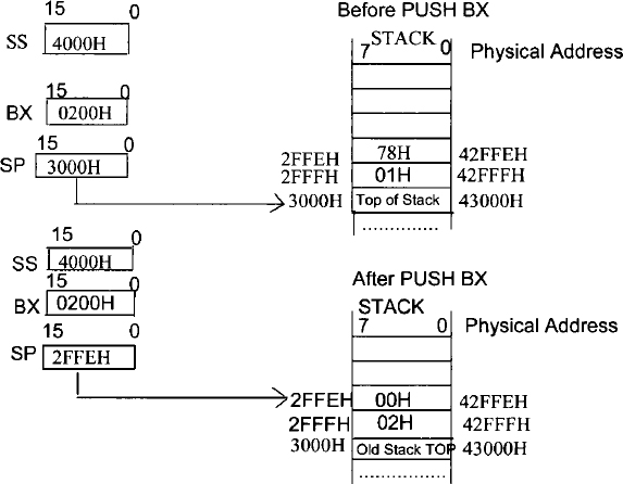
FIGURE 10.8 Pentium PUSH BX operation

FIGURE 10.9 Pentium POP AX operation
When the Pentium uses 16-bit data for PUSH and POP operations from the top of the stack, the Pentium PUSH instruction first decrements SP by 2 and then the 16-bit data is written onto the stack. Therefore, the Pentium stack grows from high to low memory addresses of the stack. On the other hand, when 16-bit data is popped from the top of the stack using the Pentium POP instruction, the Pentium reads 16-bit data from the stack into the specified register or memory, the Pentium increments the SP by 2. Note that the 20-bit physical address computed from SP and SS always points to the last data pushed onto the stack. Memory locations can also be saved and restored using PUSH and POP instructions without using any Pentium 16-bit registers. Finally, one must POP registers in the reverse order in which they are PUSHed. For example, if the registers BX, DX, and SI are PUSHed using

then the registers must be popped using

- The PUSHA instruction saves all the 16-bit register onto the stack in the following order AX, CX, DX, BX, SP, BP, SI, and DI. The SP is then decremented by 16. The PUSHAD instruction pushes all 32-bit registers onto the stack in the order EAX, ECX, EDX, EBX, ESP, EBP, ESI, and EDI. The POPA instruction pops all 16-bit registers from the stack in the order DI, SI, BP, SP, BX, DX, CX, and AX. The SP is then incremented by 16. Note that the value popped for SP is discarded. This is done to keep the SP unchanged. The POPAD instruction, on the other hand, pops all 32-bit registers from the stack in the order EDI, ESI, EBP, ESP, EBX, EDX, ECX, and EAX. The value popped for ESP is discarded.
- PUSH d8 instruction pushes 8-bit immediate data onto the stack. The SP is then decremented by 1. PUSH dl6 instruction, on the other hand, pushes 16-bit immediate data onto the stack. The SP is then decremented by 2. PUSH d32 instruction, on the other hand, pushes 32-bit immediate data onto the stack. The SP is then decremented by 4.
As an example, consider PUSH 3000H. If prior to execution of this instruction, (SS) = 4000H, (SP) = 3000H, (42FFFH) = 01H, and (42FFEH) = 05H, then after execution of PUSH 3000H, (42FFFH) = 30H, (42FFEH) = 00H, and (SP) = 2FFEH.
- XCHG has three variations: XCHG reg,reg, XCHG mem,reg, or XCHG reg, mem. Both operands cannot be memory locations. XCHG instruction is used to exchange the 8-, 16-, or 32-bit contents of two operands. Note that segment registers are not allowed in the XCHG instruction. Also, the segment for the memory location must be in DS. Consider XCHG AX,BX. This instruction exchanges the contents of 16-bit register BX with the contents of AX. If prior to execuction of the XCHG AX,BX instruction, (AX) = 2050H and (BX) = 70A0H, then after execution of the XCHG AX, BX instruction, (AX) = 70A0H, and (BX) = 2050H. Next, consider XCHG [SI], CX. If prior to excecution of the XCHG [SI], CX instruction, (SI)= 0050H, (DS) = 2000H, (CX) = 5000H, (20050H) = 56H, and (20051H) = 78H, then after execution of the XCHG [SI],CX instruction, (CX) = 7856H, (20050H) = 00H, and (20051H) = 50H.
- XLAT can be used to employ an index in a table or for code conversion. This instruction utilizes DS:BX to hold the starting address of the table in memory consisting of 8-bit data elements. AL should be the unsigned index into a table addressed by DS:BX. No flags are affected. The index in the table is assumed to be in the AL register. Note that the XLAT instruction is the same as MOV AL,[AL + BX], For example, if (BX) = 0200H, (AL) = 04H, and (DS) = 3000H, then after XLAT, the contents of location 30204H will be loaded into AL. The XLAT instruction can be used to convert from one code to another. This is illustrated in Example 10.3. The XLATB instruction should be used if BX is always resident in the DS segment. Note that DS cannot be overridden if XLATB is used while XLAT instruction allows for the possibility of segment override.
- The IN and OUT instructions of the Pentium use only the registers AL, AX, or EAX to transfer data between an I/O port (register) and the microprocessor. Two types of I/O addressing are used:
- Direct addressing
For 8-bit port: IN AL, PORT OUT PORT, AL
For 16-bit port: IN AX, PORT OUT PORT, AX
For 32-bit port: IN EAX, PORT OUT PORT, EAX
- Indirect addressing
For 8-bit port: IN AL, DX OUT DX, AL
For 16-bit port: IN AX, DX OUT DX, AX
For 32-bit port: IN EAX, DX OUT DX, EAX
Consider direct port addressing, in which the 8-, 16-, or 32-bit port address is specified directly as part of the instruction. For example, IN AL,38H inputs 8-bit data from port 38H into AL. On the other hand, the instruction IN AX,38H inputs 16-bit data from ports 38H and 39H into AX. The instruction OUT 38H,AL outputs the contents of AL to port 38H. The instruction OUT 38H,AX outputs the 16-bit contents of AX to ports 38H and 39H. For indirect port addressing, the port address is specified in the DX register. Assume that (DX) = 3124H in all the following examples.
- IN AL,DX inputs 8-bit data from an 8-bit port addressed by 3124H into AL.
- IN AX,DX inputs 16-bit data from two 8-bit ports addressed by 3124H and 3125H into AX.
- IN EAX,DX inputs 32-bit data from four 8-bit ports addressed by 3124H, 3125H, 3126H, and 3127H into EAX.
- OUT DX,AL outputs 8-bit data from AL into an 8-bit port addressed by 3124H.
- OUT DX,AX outputs 16-bit data from AX into two 8-bit ports addressed by 3124H and 3125H.
- OUT DX,EAX outputs 32-bit data from EAX into four 8-bit ports addressed by 3124H, 3125H, 3126H, and 3127H.
Indirect port addressing allows up to 65,536 ports with addresses from 0000H to FFFFH. The port addresses in indirect port addressing can be calculated dynamically in a program. For example, assume that an Pentium-based microcomputer is connected to three printers via three separate ports. Now, to output to each of the printers, separate programs are required if fixed port addressing is used. However, with indirect port addressing, one can write a general subroutine to output to the printers and then supply the address of the port for a particular printer in which data output is desired to register DX in the subroutine.
- Direct addressing
- LEA is used to load 16-bit or 32-bit offset into a specified register. As an example, LEA BX, 3000H has the same meaning as MOV BX,3000H. On the other hand, if (SI) = 2000H, then LEA BX, [SI + 4] will load 2004H into BX while MOV BX, [SI+4] will initialize BX with the contents of offset 2004H in DS. LEA can be used when address computation is desirable in a program.
LDS, LES, LFS, LGS, and LSS are similar to LEA except that they load a specified register as well as the segment register indicated. Next, consider LDS SI,[DI], This instruction loads SI and DS from memory. For example, if (DS) = 2000H, (DI) = 001 OH, (2001 OH) = 0200H, and (20012H) = 0100H, then, after LDS SI,[DI], SI and DS will contain 0200H and 0100H, respectively. Note that LDS, LES, LFS, and LGS can be used with a 32-bit extended register. Typical examples are LDS EBX,[ESI], LFS EAX, [ECX], and LSS ESP, [EDI].
- LAHF loads the lower byte of the FLAGS register into AH. This will enable the programmer to check the state of the flags. For example, if the contents of the lower byte of the FLAGS register is 43H, then after execution of the LAHF instruction, (AH) = 43H.
- SAHF is used to store the contents of AH into the lower byte of the FLAGS register. This will load a new set of flags into the FLAGS register of Figure 10.1(b).
- PUSHF pushes the lower 16 bits of the EFLAGS register onto the stack. Suppose, prior to execution of PUSHF, (SS) = 3000H, (SP) = 0000H, and (FLAGS register) = 0083H. This means that the 20-bit physical address pointing to the valid data in the stack is 30000H. After execution of the PUSHF instruction, the stack address will be decremented by 2 and (2FFFFH) = 00H, and (2FFFEH) = 83H. Note that the lower byte is pushed to the lower address and the upper byte is pushed to the higher address. This is because Pentium follows the little endian format.
- POPF pops 16 bits from the stack and places them in the FLAGS register.
EXAMPLE 10.1 Determine the effect of each of the following Pentium instructions:
Solution
(a) (ECX) = FFFFFFE7H since the most significant bit of E7H is 1, bits 8 through 31 of ECX are l's.
(b) (ECX) = 000000E7H since this instruction moves E7H to the lowest byte of ECX, and then zero extends (write 0's) from bits 8 to 31 of ECX.
(c) (AX) = 0075H since this instruction moves 75H to the lower byte of AX, and then zero-extends or write 0's from bits 8 through 15 of AX.
(d) (CL) = F2H since ES instead of SS is used as the segment register. Hence, the contents of physical address 10030H are moved to CL.
EXAMPLE 10.2 Determine the effect of each of the following Pentium instructions:
(a) PUSH [BX] if (DS) = 2000H, (BX) = 0200H, (SP) = 3000H, (SS) = 4000H, (20200H) = 20H, (20201H) = 01H, (42FFFH) = 01H, and (42FFEH) = 20H
(b) POPA if (SS) = 2000H, (SP) = 2FF0H, and (22FF0H) through (22FFFH) = 07H
Solution
(a) After execution of PUSH [BX], memory locations 42FFFH and 42FFEH will contain 01H and 20H, respectively, and the contents of SP will be 2FFEH.
(b) After POPA, a set of two consecutive bytes, 0707H from locations (22FF0H) through (22FFFH), will be loaded into Pentium's 16-bit registers in the order DI, SI, BP, SP (discarded), BX, DX, CX, and AX. The contents of SP are incremented by 16 (10H) to point to 3000H.
EXAMPLE 10.3 Assume a Pentium-based microcomputer with an ASCII keyboard is connected to port A and an EBCDIC printer is connected to port B. Suppose that it is desired to enter numerical data via the ASCII keyboard and then print them on the EBCDIC printer. Use addresses for Port A and Port B as 60H and 68H respectively. Write a Pentium assembly language program to accomplish this.
Solution
Note that numerical data entered into this microcomputer via the keyboard will be in ASCII code. Since the printer only understands EBCDIC code, an ASCII-to-EBCDIC code conversion program is required. As discussed in section 1.2.2 in Chapter 1, the ASCII codes for numbers 0 through 9 are 30H through 39H, while the EBCDIC codes for numbers 0 to 9 are FOH to F9H. The EBCDIC codes for the numbers 0 to 9 can be stored in a table starting at an offset 2030H, data can be input from the keyboard using IN AL,PORTA, then the ASCII data converted to EBCDIC using an XLAT instruction, and output to port B using OUT PORTB,AL. The assembly language for the code conversion program is

Disassembly of the program above using the MASM32 is as follows:

In the program, a table is created at offset 2030H in the data segment containing the EBCDIC codes for the BCD numbers 0 through 9. The assembler directive DB is used for the purpose. Note that assemblers generally require that hexadecimal numbers start with a digit. A 0 is typically used if the first digit of the hexadecimal number is a letter. This is done to distinguish between numbers and labels. For example, most assemblers will require the number F5H to be represented as 0F5H. This is the reason that each EBCDIC code in the table contains a leading 0.
Now, suppose that the number 4 is pushed on the ASCII keyboard connected to PORTA. The instruction IN AL,PORTA inputs 34H (ASCII for 4) into register AL. The instruction XLAT, which is equivalent to MOV AL,[BX + AL], transfers the contents of memory offset 2034H (BX + AL) into AL. This means that F4H (the contents of offset 2034H in the table) will be moved into AL. The instruction OUT PORT B,AL outputs F4H (EBCDIC for 4) into PORT B, where the EBCDIC printer is connected. Hence, the printer prints the number 4.
EXAMPLE 10.4 Write a Pentium assembly language program to clear 5010 consecutive bytes from LOW to HIGH addresses starting at offset 1000H. Assume that DS is already initialized.
Solution

The instructions INC and LOOP in the program above are described later. The instruction MOV BX, 1000H initializes BX with offset 1000H (offset 1000H is chosen arbitrarily). The instruction MOV CX,50 initializes the loop counter CX with 50. MOV BYTE PTR[BX],0 clears a memory byte addressed by the contents of BX in DS to 0. INC BX increments BX by 1 to point to the next memory byte. LOOP AGAIN decrements CX by 1 and checks for CX = 0. If CX ≠ 0, the program returns to label AGAIN. The program stops when CX = 0.
10.7.2 Arithmetic Instructions
Table 10.9 shows the Pentium arithmetic instructions. These instructions basically include addition, subtraction, signed and unsigned multiplication and division operations.
Typical microprocessors utilize common hardware to perform addition and subtraction operations for both unsigned and signed numbers. The instruction set of microprocessors typically include the same ADD and SUBTRACT instructions for both unsigned and signed numbers. The interpretations of unsigned and signed ADD and SUBTRACT operations are performed by the programmer. More detailed coverage is provided in Chapter 5.
Unsigned and Signed multiplication and division operations can be performed using various algorithms. Typical 32-bit microprocessors such as the Pentium contain separate instructions for performing these multiplication and division operations. These topics along with some multiplication and division algorithms are covered in Chapter 5.
TABLE 10.9 Pentium Arithmetic Instructions


Let us explain some of the instructions in Table 10.9.
- Consider ADD a, b. The destination operand ‘a’ can be memory or register, while the source operand ‘b’ can be memory, register, or immediate data. This instruction adds source and destination data and stores the result in destination. The operand sizes can be 8-, 16-, or 32-bit. There is no ADD mem,mem instruction. All flags in the low byte of the Flag register are affected. Typical examples include ADD CL,DL, ADD BL,[SI], ADD AX,BX, ADD CX,25A7H, ADD [BP],AX, ADD EAX,ECX, ADD BYTE PTR [SI],5 and ADD EDX,[EAX], For example, consider ADD CL, DL. If prior to execution of this instruction, (CL) = 20H, (DL) = 03H, then, after ADD CL,DL, the contents of register CL = 20 + 03 = 23H; CF = 0, PF = 0 ( result with odd parity), AF = 0 (intermediate carry from bit 3 to bit 4 is 0), ZF = 0 (nonzero result), SF = 0 (most significant bit of the result is zero), and OF = 0 since Cf (carry final) = 0 and Cp (carry previous) = 0. Note that as mentioned in Chapter 1, overflow,
 .
. - Consider ADC a, b. The destination operand ‘a’ can be memory or register while the source operand ‘b’ can be memory, register, or immediate data. This instruction adds source and destination data along with the carry flag and stores the result in destination. The operand size can be 8-, 16-, or 32-bit. There is no ADC mem,mem instruction. All flags in the low byte of the Flag register are affected. For example, if (AX) = 002016, (BX) = 030016, CF = 1, (DS) = 202016, and (20500) = 010016, then after execution of ADC AX, [BX], the contents of register AX = 0020 + 0100 + 1 = 012116; CF = 0, PF = 0 (result with odd parity), AF = 0, ZF = 0 (nonzero result), SF = 0 (most significant bit of the result is zero), and OF = 0 since Cf (carry final) = 0 and Cp (carry previous) = 0.
- Consider XADD a, b. The destination operand ‘a’ can be memory or register while the source operand ‘b’ can be memory, register, or immediate data. This instruction adds the source to the destination, stores the result in the destination, and copies the original value of the destination into the source. The operand sizes can be 8-, 16-, or 32-bit. There is no XADD mem,mem instruction. For example, if (AH) = 20H, and (BL) = 03H, then after execution of XADD AH, BL instruction, (AH) = 20H + 03H = 23H, and (BL) = 20H.
- Consider SUB a, b. The destination operand ‘a’ can be memory or register while the source operand ‘b’ can be memory, register, or immediate data. This instruction subtracts source data from destination data, and stores the result in destination. The operand sizes can be 8-, 16-, or 32-bit. There is no SUB mem, mem instruction. Typical examples include SUB BH, DL, SUB CX, DX, SUB AX, 2, SUB EAX, EBX and, SUB [EDX], ECX. All flags in the low byte of the Flag register are affected. For example, if (AH) = 03H, (BL) = 02H, then, after SUB AH,BL, the contents of register AH = 03H − 02H =01H.

The final carry is one's-complemented after subtraction to reflect the correct borrow. Hence, CF = 0. Also, PF = 0 (odd parity; number of 1's in the result is 1), AF = 1 (intermediate carry from bit 3 to bit 4 is 1), ZF = 0 (nonzero result), SF = 0 (most significant bit of the result is zero), and
 . Similarly, SUB EBX, 4 subtracts immediate data 4 from the 32-bit contents of EBX, and stores the result in EBX. All flags are affected.
 - Consider SBB a, b. The destination operand ‘a’ can be memory or register while the source operand ‘b’ can be memory, register, or immediate data. This instruction subtracts source data and the carry flag from destination data, and stores the result in destination. The operand sizes can be 8-, 16-, or 32-bit. There is no SBB mem, mem instruction. All flags in the low byte of the flag register are affected. For example, if (CH) = 03H, (DL) = 02H, and CF = 1, then, after SBB CH,DL, the contents of register CH = 03H − 02H − 1 = 00H.

The final carry is one's-complemented after subtraction to reflect the correct borrow. Hence, CF = 0. Also, PF = 1 (Even parity; number of 1's in the result is 0 and 0 is an even number), AF = 1, ZF =1 (Zero Result), SF = 0 (Most Significant bit of the result is zero), and
. - NEG reg/mem subtracts the contents of a register or a memory location from 0. In other words, this instruction finds the two's-complement of the data contained in the operand field. The operand size can be 8-, 16-, or 32-bit. Typical examples include NEG CL, NEG DX, NEG BYTE PTR [SI], NEG EAX, and NEG DWORD PTR [ECX], As an example, consider NEG ECX. If (ECX) = FFFFFFFFH, then after execution of NEG ECX, the contents of ECX are 00000001H. All flags are affected.
- Consider INC reg/mem. This instruction increments the contents of a register or a memory location by 1. The operand size can be 8-, 16-, or 32-bit. The INC reg/mem instruction affects SF, ZF, AF, OF, and PF. This instruction does not affect CF (carry flag). Typical examples include INC AH, INC BP, INC EDX, INC BYTE PTR[SI], and INC DWORD PTR[EAX].
- Consider DEC reg/mem. This instruction decrements the contents of a register or a memory location by 1. The operand size can be 8-, 16-, or 32-bit. DEC reg/mem instruction affects SF, ZF, AF, OF, and PF. Like INC mem/reg, this instruction does not affect CF (carry flag). Typical examples include DEC AH, DEC BP, DEC EDX, DEC BYTE PTR[SI], and DEC DWORD PTR[EAX].
- Consider the CMP a, b instruction. The destination operand ‘a’ can be memory or register, while the source operand ‘b’ can be memory, register, or immediate data. This instruction subtracts source from destination, providing no result of subtraction; all status flags are affected based on the result. The operand sizes can be 8-, 16-, or 32-bit. There is no CMP mem,mem instruction. Note that the SUBTRACT instruction provides the result and also affects the status flags. Consider CMP DH,BL. If prior to execution of the instruction, (DH) = 40H and (BL) = 30H, then after execution of CMP DH,BL, the flags are CF = 0, PF = 0, AF = 0, ZF = 0, SF = 0, and OF = 0; the result 10H is not provided. Suppose that it is desired to find the number of matches for an 8-bit number in a Pentium register such as DL in a data array of 50 bytes in memory pointed to by BX in DS. The following instruction sequence with CMP DL,[BX] rather than SUB DL,[BX]can be used :
In the above, if SUB DL,[BX] were used instead of CMP DL,[BX], the number to be matched needed to be loaded after each subtraction because the contents of DL would have been lost after each SUB. Since we are only interested in the match rather than the result, CMP DL,[BX] instead of SUB DL,[BX] should be used in the above.
- Consider CMPXCHG a, b. The destination operand ‘a’ can be memory or register, while the source operand ‘b’ can be memory, register, or immediate data. This instruction compares the destination with AL (for 8-bit), AX (for 16-bit) or EAX (for 32-bit). If they are equal, the contents of the source are transferred to the destination. If they are not equal, the contents of the destination are moved into AL (for 8-bit), AX (for 16-bit), or EAX (for 32-bit). The operand sizes can be 8-, 16-, or 32-bit. There is no CMPXCHG mem,mem instruction. As an example, consider CMPXCHG BL,DH. If prior to execution of this instruction, (AL) = F2H, (BL) = F2H, and (DH) = 05H, then after execution of the CMPXCHG BL,DH instruction, (BL) = 05H since (BL) = (AL) = F2H.
- DAA is used to adjust the result of adding two packed BCD numbers in AL using ADD or ADC to provide a correct packed BCD number. If, after the addition, the low 4 bits of the result in AL are greater than 9 (or if AF = 1), the DAA adds 6 to the low 4 bits of AL. On the other hand, if the high 4 bits of the result in AL are greater than 9 (or if CF = 1), DAA adds 6 to the high 4 bits in AL. Consider the following instruction sequence:

The details of the result obtained by the instruction sequence above are provided in the following:

Note that packed BCD is covered in section 1.2.3 of Chapter 1.
- DAS may be used to adjust the result of subtraction in AL of two packed BCD numbers using SUB or SBB to provide the correct packed BCD. If, after the subtraction, the low 4 bits of the result in AL is greater than 9 (or if AF = 1), then the DAS subtracts 6 from the low 4 bits of AL. On the other hand, if the high 4 bits of the result in AL are greater than 9 (or if CF = 1), then DAS subtracts 6 from AL While performing these subtractions, any borrows from low and high 4 bits are ignored. For example, consider subtracting packed BCD 55 in DL from packed BCD 94 in AL: Packed BCD 55 = 55H = 0101 01012 and Packed BCD 94 = 94H = 1001 01002.

The invalid BCD digit (F) in the low 4 bits of the result can be corrected by subtracting 6 from F:
The following Pentium instruction sequence will accomplish this:

- Consider CBW. This instruction extends the sign from the AL register to the AH register. For example, if AL = F116, then after execution of CBW, register AH will contain FF16 because the most significant bit of F1H is 1. Note that the sign extension is very useful when one wants to perform an arithmetic operation on two signed numbers of different lengths. For example, the 16-bit signed number 002016 can be added with the 8-bit signed number E1H by sign-extending E1 as follows:

- Another example of sign extension is that to multiply a signed 8-bit number by a signed 16-bit number, one must first sign-extend the signed 8-bit into a signed 16-bit number and then the instruction IMUL can be used for 16 × 16 signed multiplication. For unsigned multiplication of a 16-bit number by an 8-bit number, the 8-bit number must be zero-extended to 16 bits using logical instruction such as AND before using the MUL instruction.
For example, suppose that IMUL BX will be used to multiply the 8-bit contents of AL by the 16-bit contents of BX. If prior to execution of this instruction, (AL) = FFH = −1 and (BX) = 0002H = +2. To perform this signed multiplication, the 8-bit contents of AL must be sign-extended to 16 bits using the CBW instruction so that (AX) = FFFFH = −1. The multiplication instruction IMUL BX can then be executed so that the contents of DX:AX will be the 32-bit correct result, FFFFFFFEH (−2).
Now, to perform unsigned multiplication MUL BX with the same data, the 8-bit contents of AL must be zero-extended so that (AX) = OOFFH (+255). This can be accomplished by the instruction MOV AH,0. The instruction MUL BX can then be executed so that DX:AX will contain the correct 32-bit product, 000001FEH (+510) since (BX) = 0002H.
- CWD sign-extends the AX register into the DX register. For example, if (DX) = 08A0H and (AX) = A205H, then after execution of CWD, (DX) = FFFFH and (AX) = A205H since the most significant bit (sign bit) of AX is 1.
- CWDE sign-extends the AX register into the upper 16 bits of EAX. For example, if (EAX) = A5020277H, then after execution of CWDE, (EAX) = 00000277H since (AX) = 0277H with the sign bit (bit 15) = 0.
- CDQ sign-extends the EAX register into the EDX register. This provides a 64-bit result in EDX: EAX. For example, if (EDX) = 2F00 A7FFH and (EAX) = 0FFF FFFFH, then after execution of CDQ, (EDX) = 00000000H and (EAX) = 0FFF FFFFH.
- For 8-bit by 8-bit signed or unsigned multiplication between the contents of a memory location and AL, assembler directive BYTE PTR can be used. Example: IMUL BYTE PTR[BX], On the other hand, for 16-bit by 16-bit signed or unsigned multiplication between the 16-bit contents of a memory location and register AX, assembler directive WORD PTR can be used. Example: MUL WORD PTR[SI].
- Consider 16 × 16 unsigned multiplication, MUL WORD PTR [BX]. If (BX) = 0050H, (DS) = 3000H, (30050H) = 0002H, and (AX) = 0006H, then after MUL WORD PTR [BX], (DX) = 0000H and (AX) = 000CH.
- MUL mem/reg provides unsigned 8 × 8 or unsigned 16 × 16 multiplication. Consider MUL BL. If (AL) = 2016 and (BL) = 0216, then after MUL BL, register AX will contain 004016.
- IMUL mem/reg provides signed 8 × 8 or signed 16 × 16 multiplication. As an example, if (CL) = FDH = −310 and (AL) = FEH = −210, then, after IMUL CL, register AX contains 0006H.
- Consider IMUL DH. If (AL) = FF16 = −110 and (DH) = 0216, then, after IMUL DH, register AX will contain FFFE16 (−210).
- Consider IMUL reg16,reg16/mem16, imm8/imm16. This is an immediate signed multiplication. This is a three-operand instruction. The first operand is the 16-bit destination register, the second operand is a register or memory location containing the 16-bit multiplicand, and the third operand is either 8- or 16-bit immediate data as the multiplier. If the immediate data is 8 bits, this instruction automatically sign-extends to 16 bits before multiplication. Also, after multiplication, the low 16 bits of the product is provided. Typical example is IMUL BX, CX,2534H. Note that there is no unsigned multiplication instruction of this type.
- Consider MUL reg32/mem32. This instruction multiplies the 32-bit contents of EAX by the 32-bit contents of a 32-bit register or memory location. This is an unsigned multiplication. The 64-bit product is placed in EDX:EAX. IMUL reg32/mem32 works in the same way as the MUL reg32/mem32 except that the multiplication is signed. Typical examples include MUL EDX, IMUL EBX, and IMUL DWORD PTR [ECX].
- DIV mem/reg performs unsigned division and divides (AX) or (DX:AX) registers by reg or mem. For example, if (AX) = 0005H and (CL) = 02H, then after DIV CL, (AH) = 01H = remainder and (AL) = 02H = quotient.
- Consider DIV BL. If (AX) = 0009H and (BL) = 02H, then after DIV BL,

- IDIV mem/reg performs signed division and divides 16-bit contents of AX by an 8-bit number in a register or a memory location, or 32-bit contents of DX: AX registers by a 16-bit number in a register or a memory location. Consider IDIV CX. If (CX) = 2 and (DXAX) = −510 = FFFFFFFBH, then, after this IDIV, registers DX and AX will contain
Note that in the Pentium, after IDIV, the sign of remainder is always the same as the dividend unless the remainder is equal to zero. Therefore, in this example, because the dividend is negative (−510), the remainder is negative (−110).
- For 16-bit by 8-bit signed or unsigned division of the 16-bit contents of AX by 8-bit contents of a memory location, assembler directive BYTE PTR can be used. Example: IDIV BYTE PTR[BX], On the other hand, for 32-bit by 16-bit signed or unsigned division of the 32-bit contents of DXAX by the 16-bit contents of a memory location, assembler directive WORD PTR can be used. Example: MUL WORD PTR[SI].
- Consider IDIV WORD PTR [BX], If (BX) = 0020H, (DS) = 2000H, (20020H) = 0004H, and (DX) (AX) = 00000011H, then, after IDIV WORD PTR [BX],

- Consider DIV reg32/mem32. This instruction divides the 64-bit contents of EDX:EAX by the 32-bit contents of a register or a memory location. The division is unsigned. After the division, the 32-bit remainder is in EDX, and the 32-bit quotient is in EAX. The instruction IDIV reg 32/mem32 works in the same way as the DIV reg32/mem32 except that the division is signed. Typical examples include IDIV EBX, DIV DWORD PTR [ESI], and DIV ECX.
- Consider the AAA instruction. The addition of two one-digit ASCII numbers will not provide meaningful information. For example, if 35H (ASCII for 5) is added with 39H (ASCII for 9), the sum will be 6EH. This is not a useful number. The result of adding 5 and 9 in ASCII should have been the ASCII equivalent of 14, which is 3134H. If the sum 6EH is saved in AL, and if the instruction AAA is executed, the contents of AL (6EH) will be converted to correct unpacked BCD (0104H) in AX. Note that the AAA instruction first checks the contents of AL, adjusts the lower four bits to provide the correct BCD result. Furthermore, the AAA instruction then clears the upper four bits of AL to 0. Finally, the AAA instruction clears AH to 0 (AH = 00H) if the result is less than or equal to 9, and adds 1 to AH (AH = 01H) if the result is greater than 9. Only CF and AF are affected.
The following example illustrates how the AAA instruction provides the correct BCD result:

Since AAA clears upper 4 bits to 0, AL will contain 04H.
Also, because the low 4 bits of AL are greater than 9 (EH) prior to the execution of AAA, the contents of AH = 01H after execution of AAA. Hence, (AX) after execution of AAA = 0104H. Note that 0104H can be converted to 3134H (ASCII for 14H) by adding 3030H.
Next, consider adding 32H (ASCII for 2) and 35H (ASCII for 5). The result will be 67H. If the result is saved in AL and the AAA instruction is executed, AX will contain 0007H as follows: (AL) = 67H = 0110 0111 will be converted to 07H in AL by the AAA instruction. Also, since the low 4 bits of AL are 7 (less than 9), the AAA instruction clears AH to 0 so that (AH) = 00H. Hence, (AX) = 0007H.
Numerical data received by a Pentium-based microcomputer from an ASCII keyboard is in ASCII codes, which for numbers 0 to 9 is 30H through 39H. Two 8-bit data items can be entered into a Pentium-based microcomputer via the ASCII keyboard. The ASCII codes for these data items (with 3 as the upper 4 bits of each data byte) can be added. The AAA instruction can then be used to provide the correct unpacked BCD. Suppose that the ASCII codes for 6 (36H) and 5 (35H) are entered into a Pentium-based microcomputer via the keyboard. These ASCII codes can be added and then the result can be adjusted to provide the correct unpacked BCD using the AAA instruction. The unpacked BCD can then be converted to ASCII by adding 3030H. The following instruction sequence will accomplish this:

Note that in to print the result 11 on an ASCII printer, (AX) = 0101H is added with 303OH to provide 3131H, the ASCII code for 11. Note that unpacked BCD numbers are covered in section 1.2.3 in Chapter 1.
- Consider the AAS instruction. This instruction is similar to AAA except that it is used to adjust AX after an ASCII subtraction using SUB or SBB. Suppose that (AX) = 0038H and (DH) = 32H = ASCII for 2. With this data, after execution of SUB AL,DH, the contents of AL will be 06H. After execution of AAS, the result is not changed since the the low 4 bits of AL (6) are less than 9. Hence, the final value of AX is 0006H. Adding 3030H to AX, the contents of AX will be 3036H (ASCII for the number 06).
Now, suppose that (DH) = 39H and (AX) = 0035H. After execution of SUB AL,DH, register AL will contain FCH as follows:
After execution of AAS, the upper 4 bits of AL (F) are cleared to zero so that (AL) = OCH, and the number in AH is decremented by 1 so that AH will contain FFH (−1). Also, after execution of the AAS instruction, 6 is subtracted from C (since C is greater than 9) as follows:

Hence, AL will contain 06H, and FFH in AH indicates that a borrow has occurred. Note that 5 − 9 = −6 (after BCD correction). AL will contain 36H (ASCII for 6) after adding 30H to AL.
- Consider the AAM instruction. The AAM instruction adjusts the product of two unpacked BCD digits in AX. If (AL) = 03H (unpacked BCD for 3) = 000000112 and (CH) = 08H (unpacked BCD for 8) = 0000 10002, then, after MUL CH, the contents of AX are 00000000000110002 (0018H), and after using AAM, the contents of AX are 00000010000001002 = unpacked BCD 0204. The following instruction sequence accomplishes this:

Note that the Pentium does not allow multiplication of two ASCII codes. Therefore, before multiplying two ASCII bytes received from an ASCII keyboard, one must make the upper 4 bits of each one of these bytes zero, multiply them as two unpacked BCD digits, and then use AAM to convert the binary product to unpacked BCD. The unpacked BCD product can be converted back to ASCII by adding the product with 3030H. For example, by adding 3030H with 0204H, the result 3234H (ASCII for 24) is obtained. The result 24 in decimal can then be printed on an ASCII printer.
- Consider the AAD instruction. The AAD instruction converts two unpacked BCD digits in AH and AL to an equivalent binary number in AL. AAD must be used before dividing two unpacked BCD digits in AX by an unpacked BCD byte. For example, consider dividing (AX) = unpacked BCD 0408H (48H packed BCD) by (DH) = 06H. (AX) must first be converted to binary by using AAD in order to use the binary division instruction DIV. The register AX will then contain 0030H = 48H Packed BCD. After DIV DH, the contents of AL = quotient = 08H (unpacked BCD), and the contents of AH = remainder = 00H. The following instruction sequence will accomplish this:
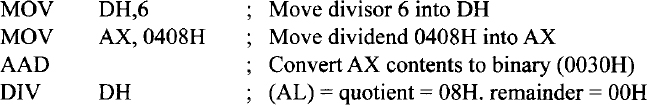
Note that packed and unpacked BCD are covered in section 1.2.3 in Chapter 1.
- One-dimensional arrays (tables) can be be accessed using Pentium MOV instructions with the appropriate addressing mode. For example, consider a table of of five elements containing 5 bytes stored starting at an offset 2000H in DS. The table is stored in memory such that 2000H points to element 0, 2001H points to element 1, and 2004H points to element 4. This is depicted in Figure 10.10. An index register such as DI can be initialized with the element number to read an element from this array into an 8-bit register such as CL. For example, if (DI) = 2, then MOV CL,[2000H + DI] will load element 2 from offset 2002H into CL. On the other hand, if (DI) = 4, then MOV CL,[2000H + DI] transfers element 4 into CL.
Suppose that an array of 10 elements containing 32-bit data words is stored starting at an offset 4000H. This means that 4 bytes are needed to store each element. That is, offset 4000H through 4003H will contain element 0 while offset 4024H through 4027H will store element 9. Hence, offset 4000H will contain element 0, offset 4004 will contain element 1, Offset 4008 will contain element 2, and so on. The based indexed addressing mode with a scaling of 4 can be used to access the array since the element size is 4 bytes (32 bits). Now, to move element 2 into EAX, the following instruction sequence can be used:
In the instruction sequence above, the starting offset (4000H) of the table is first loaded into a 32-bit register such as ECX. The element number (2) is then transferred to EDX. Register EDX is scaled by 4 since each element is 4 bytes (32 bits). The value of element 2 is then loaded into a 32-bit register such as EAX using MOV EAX,[ECX + EDX*4]. Note that arithmetic operations can be performed on array elements in a table. This is illustrated in Example 10.18.

FIGURE 10.10 One dimensional array stored in memory
Next, consider two-dimensional arrays or matrices. For example, assume a 2 × 3 matrix (two rows and three columns) as follows:
Since memory is one-dimensional, this matrix is stored in memory using column-major or row-major ordering. In column-major ordering the elements are stored column by column, starting with the first column:
a[0,0]
a[1,0]
a[0,1]
a[1,1]
a[0,2]
a[1,2]
In row-major ordering the elements are stored in memory row by row, starting with the first row:
a[0,0]-- column 0 (start of array)
a[0,1]-- column 1
a[0,2]-- column 2
a[1,0]-- column 0
a[1,1]-- column 1
a[1,2]-- column 2
Since row-major ordering and subscripts start with 0 in C language, the same convention will be used here.
Assume that an offset 2000H addresses the first element a[0, 0] of the array. This means that offset 2000H points to the first element of the array, a[0, 0]. In the C language, which uses row-major ordering and subscripts starting with zero, one can express displacement d of an element at row i and column j as d = (i*t + j) * s, where t is the total number of columns and s is the element size (1 for byte, 2 for 16-bit, and 4 for 32-bit).
Now, to find the displacement of element a[1, 0] assuming that each element is 16-bit, the offset can be determined as follows. Note that i = 1,j = 0, t = 3 (since 2 × 3 matrix), and s=2 (16-bit element). Hence, d = (1*3 + 0)*2 = 6. Therefore, the offset where element a[1, 0] is stored = 2000H + 6 = 2006H. Hence, the matrix above with row-major ordering can be stored with starting offset 2000H as follows:
| 2000H | a[0,0] |
| 2002H | a[0,1] |
| 2004H | a[0,2] |
| 2006H | a[1,0] |
| 2008H | a[1,1] |
| 200AH | a[1,2] |
Next to load element, a[1, 0] into BX from the array, the following Pentium instruction sequence can be used:

Note that arithmetic operations can be performed on array elements of a two-dimensional matrix. This is illustrated in Example 10.19.
EXAMPLE 10.5 Determine the effect of each of the following Pentium instructions:
(a) CBW (b) CDQ (c) IMUL BX, DX, OFFH (d)DIVCH Assume the following data prior to execution of each of these instructions independently (assume that all numbers are in hexadecimal): (CX) = 0300H, (EAX) = A2130091H, and (EDX) = 52F10002H.
Solution
(a) CBW sign-extends the AL register into the AH register. Because the content of AL is 91H, the sign bit is 1. Therefore, after CBW, (AX) = FF91H.
(b) CDQ sign-extends EAX into EDX, providing a 64-bit result EDX:EAX. Since the sign bit (the most significant bit of EAX is 1, the content of EDX is FFFFFFFFH.
(c) IMUL BX,DX,0FFH first sign-extends FFH to FFFFH (16-bit) and interprets this as a signed number (−1). It then performs signed multiplication between the contents of DX (0002H) and FFFFH and provides the low 16 bis of the answer as FFFEH (−2) in BX. The upper 16 bits of the product are discarded.
(d) Before unsigned division, CH contains 0310 and AX contains 14510 (91H). Therefore, after DIV CH, (AH) = remainder = 01H and (AL) = quotient = 4810 = 30H.
EXAMPLE 10.6 Write a Pentium assembly language program for the following C language program structure:
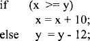
Assume that x and y are addresses of two 16-bit signed integers.
Solution
Assume addresses x and y are initialized with the contents of the Pentium memory locations addressed by offsets BX and SI in segment register DS.
EXAMPLE 10.7 Write a Pentium assembly language program for the following C language program structure:
sum = 0;
for ( i = 0; i <= 9; i = i + 1)
sum = sum + a[i];
Assume that sum is the address of the 16-bit result.
Solution
Assume register SI holds the address of the first element of the array while BX contains the offset of the sum.

EXAMPLE 10.8 Write a Pentium assembly program to find (X2)/255 where X is an 8-bit signed number stored in CH. Store the 16-bit result onto the stack. Initialize SS and SP to 1000H and 2000H, respectively.
Solution
EXAMPLE 10.9 What are the remainder, quotient, and registers containing them after execution of the following Pentium assembly language program?
Solution

EXAMPLE 10.10 Write a Pentium assembly language program to add two 16-bit numbers in CX and DX and store the result in offset 1000H addressed by DI.
Solution
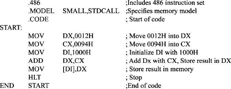
EXAMPLE 10.11 Write a Pentium assembly language program to add four 16-bit numbers stored in consecutive locations starting at a 32-bit offset pointed to by EBX. Store the 16-bit result in AX. Use ADC instruction for addition. Initialize DS to 5000H, and EBX to 00001000H.
Solution

EXAMPLE 10.12 Write a Pentium assembly language program to add two 64-bit numbers. Assume that ESI and EDI contain the starting offsets of the numbers. Store the result in memory pointed to by EDI. Initialize DS to 3000H, ESI to 0, and EDI to 8.
Solution

In the program above, ESI and EDI are added with 4 using the INC instruction four times rather than ADD SI,4 and ADD DI,4. This is because the INC instruction does not affect the carry flag, whereas the ADD instruction does. Note that the ADC [EDI], EAX instruction is used to add two 32-bit data with the carry flag. For adding high 32-bit numbers, the carry flag must not be altered. Hence, INC rather than ADD is used. Also, JNZ START checks whether ZF is 0 or 1. Note that ZF =1 when DEC DX decrements DX to 0. In that case, the program will execute HLT and stop. However, if ZF = 0 (i.e., DX is not decremented to 0 by DEC DX), the program loops back to START.
EXAMPLE 10.13 Write a Pentium assembly language program to multiply two 32-bit unsigned numbers to provide a 64-bit result. Assume that the two numbers are stored in ECX and EDX.
Solution


EXAMPLE 10.14 Write a Pentium assembly language program to multiply two 8-bit signed numbers stored in the same 16-bit register, AX; AH holds one number and AL holds the other number. Store the 16-bit result in DX.
Solution

EXAMPLE 10.15 Write a Pentium assembly program that converts a temperature (signed) from Fahrenheit degrees stored at an offset contained in SI to Celsius degrees. The program stores the 8-bit integer, which is part of the result at an offset contained in DI. Assume that the temperature can be represented by one byte and that DS is already initialized. The source byte is assumed to reside at offset 2000H in the data segment, and the destination byte at an offset of 3000H in the same data segment. Use the formula C = (F−32)/9 × 5
Solution
EXAMPLE 10.16 Write a Pentium assembly program to implement the following C language program loop:
sum = 0;
for (i = 0; i <=99; i = i + 1)
sum = sum + x[i] * y[i];
The assembly language program will compute ![]() where the Xi's and Yi‘s are signed 8-bit numbers stored at offsets 4000H and 5000H, respectively. Initialize DS at 2000H. Store the 16-bit result in DX. Assume no overflow.
where the Xi's and Yi‘s are signed 8-bit numbers stored at offsets 4000H and 5000H, respectively. Initialize DS at 2000H. Store the 16-bit result in DX. Assume no overflow.
Solution
EXAMPLE 10.17 Write a Pentium assembly language program to add two words; each contains two ASCII digits. The first word is stored in two consecutive locations with the low byte pointed to by SI at offset 0300H, and the second word is stored in two consecutive locations with the low byte pointed to by DI at offset 0700H. Store the unpacked BCD result in memory location pointed to by DI.
Solution


EXAMPLE 10.18 Write a Pentium assembly language program to add all the elements in a table containing eight 16-bit elements stored in memory addressed by offset 00005000H. Store the 16-bit result in DX.
Solution

EXAMPLE 10.19 Write a Pentium assembly language program to find the trace (sum of the elements in the diagonal) of a 3 × 3 matrix containing 16-bit words. Store the 16-bit result in DI. Assume that the matrix is stored in row-major ordering starting at an offset 1000H:
| 1000H | a[0,0] |
| 1002H | a[0,1] |
| 1004H | a[0,2] |
| 1006H | a[1,0] |
| 1008H | a[1,1] |
| 100AH | a[1,2] |
| 100CH | a[2,0] |
| 100EH | a[2,1] |
| 1010H | a[2,2] |
Note that trace = a[0, 0] + a[1, 1] + a[2, 2] and displacement, d = (i *t +j)*s = i*t*s + j*s where i = row number, j = column number, t = total number of columns in the matrix, and s = element size. In this example, t = 3 for 3×3 matrix, and s = 2 since each element is 16-bit. Hence, d = 3*(2*i) + 2*j = 6 * i + 2 *j. Hence, the offset where each element, aij will be stored = A0 + 6*i +2*j where A0 = starting offset of the array, i = row number, and j = column number.
Solution