Chapter 6: Specialized Computing Domains
Most computer users are, at least superficially, familiar with key performance-related attributes of personal computers and smart digital devices, such as processor speed and random-access memory (RAM) size. This chapter explores the performance requirements of computing domains that tend to be less directly visible to users, including real-time systems, digital signal processing, and graphics processing unit (GPU) processing.
We will examine the unique computing features associated with each of these domains and review some examples of modern devices implementing these concepts.
After completing this chapter, you will be able to identify application areas that require real-time computing and you will understand the uses of digital signal processing, with an emphasis on wireless communication. You will also understand the basic architecture of modern GPUs and will be familiar with some modern implementations of components in the computing domains discussed in this chapter.
This chapter covers the following topics:
- Real-time computing
- Digital signal processing
- GPU processing
- Examples of specialized architectures
Real-time computing
The previous chapter provided a brief introduction to some of the requirements of real-time-computing in terms of a system's responsiveness to changes in its inputs. These requirements are specified in the form of timing deadlines that limit how long the system can take to produce an output in response to a change in its input. This section will look at these timing specifications in more detail and will present the specific features real-time computing systems implement to ensure timing requirements are met.
Real-time computing systems can be categorized as providing soft or hard guarantees of responsiveness. A soft real-time system is considered to perform acceptably if it meets its desired response time most, but not necessarily all, of the time. An example of a soft real-time application is the clock display on a cell phone. When opening the clock display, some implementations momentarily present the time that was shown the last time the clock display was opened before quickly updating to the correct, current time. Of course, users would like the clock to show the correct time whenever it is displayed, but momentary glitches such as this aren't usually seen as a significant problem.
A hard real-time system, on the other hand, is considered to have failed if it ever misses any of its response-time deadlines. Safety-critical systems such as airbag controllers in automobiles and flight control systems for commercial aircraft have hard real-time requirements. Designers of these systems take timing requirements very seriously and devote substantial effort to ensuring the real-time processor satisfies its timing requirements under all possible operating conditions.
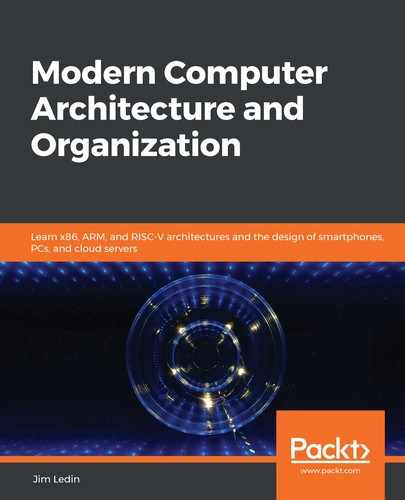
The control flow of a simple real-time system is shown in the following screenshot:
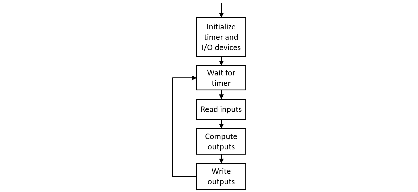
Figure 6.1: Real-time system control flow
Figure 6.1 represents a real-time computing system using a hardware interval timer to control the time sequencing of its operation. A down-counting interval timer performs a repetitive cycle of the following steps:
- Load the counter register with a predefined numeric value.
- Decrement the counter at a fixed clock rate.
- When the count reaches zero, generate an event such as setting a bit in a register or triggering an interrupt.
- Go back to Step 1.
An interval timer generates a periodic sequence of events with timing accuracy that depends on the accuracy of the system clock, which is often driven by a quartz crystal. By waiting for the timer event at the top of each loop, the system in Figure 6.1 begins each execution pass at fixed, equal time intervals.
To satisfy the demands of hard real-time operation, the execution time of the code inside the loop (the code contained in the Read inputs, Compute outputs, and Write outputs blocks in Figure 6.1) must always be less than the timer interval. Prudent system developers ensure that no path through the code results in execution time anywhere close to the hard real-time limit. A conservative system design rule might insist the longest execution path for code inside the loop consumes no more than 50% of the timer interval.
Practical real-time systems constructed in this configuration might be based on an 8-, 16-, or 32-bit processor running at a clock frequency in the tens to hundreds of MHz. The timer employed in the main loop of such systems generates events at a developer-selected frequency, often in the range 10 to 1000 Hz.
The code represented in Figure 6.1 runs directly on the processor hardware with no intervening software layers. This configuration contains no operating system of the type described in Chapter 5, Hardware-Software Interface. A sophisticated real-time application is likely to have more extensive needs than can be met by this simplistic architecture, making the use of a real-time operating system attractive.
Real-time operating systems
A real-time operating system (RTOS) contains several features superficially similar to the general-purpose operating systems discussed in Chapter 5, Hardware-Software Interface. An RTOS design differs significantly from general-purpose operating systems, however, in that all RTOS aspects—from kernel internals, to device drivers, to system services— are focused on meeting hard real-time requirements.
Most RTOS designs employ preemptive multithreading, often referred to as multitasking in RTOS literature. The terms task and thread are somewhat synonymous in the RTOS context, so for consistency we will continue to use the term thread to indicate an RTOS task.
RTOS designs at the lower end of the sophistication scale typically support multithreading within the context of a single application process. These simpler RTOSes support thread prioritization but often lack memory protection features.
More sophisticated RTOS architectures provide multiple thread privilege levels and operating system features such as memory protection, in addition to prioritized, preemptive multithreading. These RTOSes allow multiple processes to be in the Running state simultaneously, each potentially containing several threads. In protected memory systems, kernel memory access by application threads is prohibited and applications cannot reach into each other's memory regions. Many RTOSes support multi-core processor architectures.
RTOS environments, from lower to higher levels of sophistication, provide several data structures and communication techniques geared toward efficient data transfer between threads, and to support controlled access to shared resources. Some examples of these features are as follows:
- Mutex: A mutex (short for mutual exclusion) is a mechanism for a thread to claim access to a shared resource, without blocking the execution of other threads. In its simplest form, a mutex is a variable accessible to all threads that has the value 0 when the resource is free and 1 when the resource is in use. A thread that wants to use the resource reads the current value of the mutex variable and, if it is 0, sets it to 1 and performs the operation with the resource. After completing the operation, the thread sets the mutex back to 0. There are, however, some potential problems with mutexes:
Thread preemption: Let's say a thread reads the mutex variable and sees that it is 0. Because the scheduler can interrupt an executing thread at any time, that thread might be interrupted before it has a chance to set the mutex to 1. A different thread then resumes execution and takes control of the same resource because it sees the mutex is still 0. When the original thread resumes, it finishes setting the mutex to 1 (even though, by now, it has already been set to 1). At this point, both threads incorrectly believe they have exclusive access to the resource, which is likely to lead to serious problems.
To prevent this scenario, many processors implement some form of a test-and-set instruction. A test-and-set instruction reads a value from a memory address and sets that location to 1 in a single, uninterruptable (also referred to as atomic) action. In the x86 architecture, the BTS (bit test and set) instruction performs this atomic operation. In processor architectures that lack a test-and-set instruction (such as the 6502), the risk of preemption can be eliminated by disabling interrupts before checking the state of the mutex variable, then re-enabling interrupts after setting the mutex to 1. This approach has the disadvantage of reducing real-time responsiveness while interrupts are disabled.
Priority inversion: Priority inversion occurs when a higher-priority thread attempts to gain access to a resource while the corresponding mutex is held by a lower-priority thread. In this situation, RTOS implementations generally place the higher-priority thread in a blocked state, allowing the lower-priority thread to complete its operation and release the mutex. The priority inversion problem occurs when a thread with a priority between the upper and lower levels of the two threads begins execution. While this mid-priority thread is running, it prevents the lower-priority thread from executing and releasing the mutex. The higher-priority thread must now wait until the mid-priority thread finishes execution, effectively disrupting the entire thread prioritization scheme. This can lead to failure of the high-priority thread to meet its deadline.
One method to prevent priority inversion is priority inheritance. In an RTOS implementing priority inheritance, whenever a higher-priority thread (thread2) requests a mutex held by a lower-priority thread (thread1), thread1 is temporarily raised in priority to the level of thread2. This eliminates any possibility of a mid-priority thread delaying the completion of the (originally) lower-priority thread1. When thread1 releases the mutex, the RTOS restores its original priority.
Deadlock: Deadlock can occur when multiple threads attempt to lock multiple mutexes. If thread1 and thread2 both require mutex1 and mutex2, a situation may arise in which thread1 locks mutex1 and attempts to locks mutex2, while at the same time thread2 has already locked mutex2 and attempts to lock mutex1. Neither task can proceed from this state, hence the term deadlock. Some RTOS implementations check the ownership of mutexes during lock attempts and report an error in a deadlock situation. In simpler RTOS designs, it is up to the system developer to ensure deadlock cannot occur.
- Semaphore: A semaphore is a generalization of the mutex. Semaphores can be of two types: binary and counting. A binary semaphore is similar to a mutex except that rather than controlling access to a resource, the binary semaphore is intended to be used by one task to send a signal to another task. If thread1 attempts to take semaphore1 while it is unavailable, thread1 will block until another thread or interrupt service routine gives semaphore1.
A counting semaphore contains a counter with an upper limit. Counting semaphores are used to control access to multiple interchangeable resources. When a thread takes the counting semaphore, the counter increments and the task proceeds. When the counter reaches its limit, a thread attempting to take the semaphore blocks until another thread gives the semaphore, decrementing the counter.
Consider the example of a system that supports a limited number of simultaneously open files. A counting semaphore can be used to manage file open and close operations. If the system supports up to 10 open files and a thread attempts to open an 11th file, a counting semaphore with a limit of 10 will block the file open operation until another file is closed and its descriptor becomes available.
- Queue: A queue (also referred to as a message queue) is a unidirectional communication path between processes or threads. The sending thread places data items into the queue and the receiving thread retrieves those items in the same order they were sent. The RTOS synchronizes accesses between the sender and receiver so the receiver only retrieves complete data items. Queues are commonly implemented with a fixed-size storage buffer. The buffer will eventually fill and block further insertions if a sending thread adds data items faster than the receiving thread retrieves them.
RTOS message queues provide a programming interface for the receiving thread to check if the queue contains data. Many queue implementations also support the use of a semaphore to signal a blocked receiving thread when data is available.
- Critical section: It is common for multiple threads to require access to a shared data structure. When using shared data, it is vital that read and write operations from different threads do not overlap in time. If such an overlap occurs, the reading thread may receive inconsistent information if it accesses the data structure while another thread is in the midst of an update. The mutex and semaphore mechanisms provide options for controlling access to such data structures. The use of a critical section is an alternate approach that isolates the code accessing the shared data structure and allows only one thread to execute that sequence at a time.
A simple method to implement a critical section is to disable interrupts just before entering a critical section and re-enable interrupts after completing the critical section. This prevents the scheduler from running and ensures the thread accessing the data structure has sole control until it exits the critical section. This method has the disadvantage of impairing real-time responsiveness by preventing responses to interrupts, including thread scheduling, while interrupts are disabled.
Some RTOS implementations provide a more sophisticated implementation of the critical section technique, involving the use of critical section data objects. Critical section objects typically provide options to allow a thread to either enter a blocked state until the critical section becomes available or test if the critical section is in use without blocking. The option for testing critical section availability allows the thread to perform other work while waiting for the critical section to become free.
This section provided a brief introduction to some of the communication and resource management capabilities common to RTOS implementations. There are far more real-time computing systems in operation today than there are PCs we think of as computers. General-purpose computers represent less than 1% of the digital processors produced each year. Devices ranging from children's toys, to digital thermometers, to televisions, to automobiles, to spacecraft contain at least one, and often contain dozens of embedded processors, each running some type of RTOS.
The next section introduces processing architectures used in the processing of digital samples of analog signals.
Digital signal processing
A digital signal processor (DSP) is optimized to perform computations on digitized representations of analog signals. Real-world signals such as audio, video, cell phone transmissions, and radar are analog in nature, meaning the information being processed is the response of an electrical sensor to a continuously varying voltage. Before a digital processor can begin to work with an analog signal, the signal voltage must be converted to a digital representation by an analog-to-digital converter (ADC). The following section describes the operation of ADCs and digital-to-analog converters (DACs).
ADCs and DACs
An ADC measures an analog input voltage and produces a digital output word representing the input voltage. ADCs often use a DAC internally during the conversion process. A DAC performs the reverse operation of an ADC, converting a digital word to an analog voltage.
A variety of circuit architectures are used in DAC applications, generally with the goal of achieving a combination of low cost, high speed, and high precision. One of the simplest DAC designs is the R-2R ladder, shown here in a 4-bit input configuration:
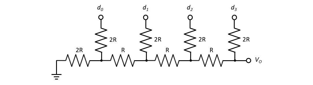
Figure 6.2: R-2R ladder DAC
This DAC uses a 4-bit data word on the inputs d0-d3 to generate an analog voltage, VO. If we assume each bit of the 4-bit word d is driven at either 0 V (for a 0-bit) or 5 V (for a 1-bit), the output VO equals (d / 24) * 5 V, where d is a data value in the range 0 to 15. An input word of 0 has an output of 0 V, and an input word of 15 has an output of (15/16) * 5V = 4.6875V. Intermediate values of d produce equally spaced output voltages at intervals of (1/16) * 5V = 0.3125V.
An ADC can use an internal DAC in this manner (though usually with a larger number of bits, with a correspondingly finer voltage resolution) to determine the digital equivalent of an analog input voltage.
Because the analog input signal can vary continuously over time, ADC circuits generally use a sample-and-hold circuit to maintain a constant analog voltage during the conversion process. A sample-and-hold circuit is an analog device with a digital hold input signal. When the hold input is inactive, the sample-and-hold output tracks the input voltage. When the hold input is active, the sample-and-hold circuit freezes its output voltage at the input voltage that was present at the moment the hold signal was activated.
With its input held constant, the ADC uses its DAC to determine the digital equivalent of the input voltage. To make this determination, the ADC uses a comparator, which is a circuit that compares two analog voltages and produces a digital output signal indicating which is the higher voltage. The ADC feeds the sample-and-hold output voltage into one input of the comparator and the DAC output into the other input, as shown in the following diagram, in which the DAC input word size is n bits:

Figure 6.3: ADC architecture
The job of the ADC is to determine the DAC input word that causes the comparator to change state. A simple way to do this is to count upward from zero, writing each numeric value to the DAC inputs and observing the comparator output to see if it changed state. The DAC output that first causes the comparator to change state is the smallest DAC output voltage that is greater than the sample-and-hold output voltage. The actual sampled analog voltage is between this DAC output and the DAC output from a data word one count smaller. This ADC configuration is called a counter type ADC.
While simple in concept, the counter type ADC can be quite slow, especially if the word size is large. A faster method is to sequentially compare each bit in the DAC data word, beginning with the most significant bit. Starting with a data word of 1000b in our 4-bit example, the first comparator reading indicates if the analog input voltage is above or below the DAC voltage midpoint. This determines if bit d3 of the ADC reading is 0 or 1. Using the now-known value of d3, d2 is set to 1 to indicate which quarter of the full-scale range the input voltage lies within. This procedure is repeated to sequentially determine each of the remaining bits, ending with the least significant bit.
This ADC conversion technique is referred to as successive approximation. A successive approximation ADC is much faster than a counter type ADC. In our example, the maximum possible number of comparisons drops from 16 to 4. In a 12-bit successive approximation ADC, the potential number of comparisons drops from 4,096 to 12. Successive approximation ADCs are available with resolutions from 8 to 18 bits, with maximum conversion rates up to several MHz.
ADCs and DACs are characterized by resolution and maximum conversion speed. The resolution of an ADC or DAC is determined by the number of bits in its data word. The maximum conversion speed determines how quickly the ADC or DAC can produce sequential outputs.
To process real-time data, an ADC produces a sequence of measurements at periodic time intervals for use as input to further processing. Requirements for data word resolution and sample rate vary widely depending on the particular DSP application. Some examples of standard digitized analog data formats are as follows:
- Compact disk digital audio is sampled at 44.1 kHz with 16 bits per sample in two channels, corresponding to the left and right speakers.
- Video cameras measure the analog light intensity received at each pixel in a two-dimensional array and convert the reading to a digital word, usually 8 bits wide. Separate closely spaced sensors with color filters produce red, green, and blue measurements for each pixel in the image. The complete dataset for a single pixel consists of 24 bits, composed of three 8-bit color values. A single image can contain tens of millions of pixels, and video cameras typically produce 30 to 60 frames per second. Because digital video recording produces such an enormous quantity of data, compression algorithms are generally used to reduce storage and transmission requirements.
- A mobile phone contains a radio frequency transceiver that down-converts the received radio frequency signal to a frequency range suitable for input to an ADC. Typical parameters for a mobile phone ADC are 12 bits of resolution and a sample rate of 50 MHz.
- An automotive radar system samples radio frequency energy reflected from nearby obstacles with a resolution of 16 bits at a rate of 5 MHz.
DSP hardware features
DSPs are optimized to execute signal processing algorithms on digitized samples of analog information. The dot product is a fundamental operation used in many algorithms performed by DSPs. If A and B are two equal-length vectors (a vector is a one-dimensional array of numeric values), the dot product of A and B is formed by multiplying each element of A by the corresponding element of B, and summing the resulting products. Mathematically, if the length of each vector is n (indexed from 0 to n-1), the dot product of the vectors is as follows:

The repetitive nature of the dot product calculation provides a natural path for performance optimization in digital systems. The basic operation performed in the dot product computation is called multiply-accumulate (MAC).
A single MAC consists of multiplying two numbers together and adding the result to an accumulator, which must be initialized to zero at the beginning of the dot product calculation. The mathematical performance of DSP chips is commonly measured in terms of MACs per second. Many DSP architectures are capable of performing one MAC per instruction clock cycle.
To perform a MAC on every clock cycle, a DSP cannot dedicate separate clock cycles to read a MAC instruction from program memory, read each of the vector elements to be multiplied from data memory, compute the product, and add it to the accumulator. All of these things must happen in one step.
The von Neumann architecture, introduced in Chapter 1, Introducing Computer Architecture, uses a single memory region for program instructions and data. This configuration results in a limitation known as the von Neumann bottleneck, resulting from the need to pass program instructions and data values sequentially across a single processor-to-memory interface.
This effect can be mitigated by using an architecture that separates program instructions and data storage into two separate memory regions, each with its own processor interface. This configuration, called the Harvard architecture, allows program instruction and data memory access to occur in parallel, enabling instructions to execute in a smaller number of clock cycles.
A DSP with a Harvard architecture must perform two data memory accesses to retrieve the elements of the A and B vectors to be multiplied in a MAC operation. This normally requires two clock cycles, failing to meet the performance goal of one MAC per clock cycle. A modified Harvard architecture supports the use of program memory to store data values in addition to instructions. In many DSP applications, the values of one of the vectors (let's say the A vector) involved in the dot product are constant values known at the time the application is compiled. In a modified Harvard architecture, the elements of the A vector can be stored in program memory and the elements of the B vector, representing input data read from an ADC, are stored in data memory.
To perform each MAC operation in this architecture, one element of the A vector is read from program memory, one element of the B vector is read from data memory, and the accumulated product is stored in an internal processor register. If the DSP contains cache memory for program instructions, the MAC instruction performing each step of the dot product will be read from cache once the first MAC operation reads it from program memory, avoiding further memory access cycles to retrieve the instruction. This configuration (modified Harvard architecture with program instruction caching) enables single-cycle MAC operations for all iterations of the dot product once the first MAC has completed. Since the vectors involved in real-world dot product computations commonly contain hundreds or even thousands of elements, the overall performance of the dot product operation can closely approach the ideal of one MAC per DSP clock cycle.
A DSP can be categorized as having a fixed-point or a floating-point architecture. Fixed-point DSPs use signed or unsigned integers to perform mathematical operations such as MAC. Fixed-point DSPs are generally less costly than floating-point DSPs. However, fixed-point mathematics has the potential for numeric issues such as overflow, which can manifest by exceeding the range of the dot product accumulator.
To reduce the possibility of overflow, DSPs often implement an extended range accumulator, sometimes 40 bits wide in a 32-bit architecture, to support dot products on lengthy vectors. Due to concerns regarding overflow and related numerical issues, programming fixed-point DSPs requires extra effort to ensure these effects don't result in unacceptable performance degradation.
Floating-point DSPs often use a 32-bit wide numeric format for internal calculations. Once an integer ADC reading has been received by the DSP, all further processing is performed using floating-point operations. By taking advantage of floating-point operations, the potential for issues such as overflow is drastically reduced, resulting in quicker software development cycles.
The use of floating-point also improves the fidelity of computation results, realized in terms of improved signal-to-noise ratio (SNR) in comparison to an equivalent fixed-point implementation. Fixed-point calculations quantize the result of each mathematical operation at the level of the integer's least significant bit. Floating-point operations generally maintain accurate results from each operation to a small fraction of the corresponding fixed-point least significant bit.
Signal processing algorithms
Building upon our understanding of DSP hardware and the operations it supports, we will next look at some examples of digital signal processing algorithms in real-world applications.
Convolution
Convolution is a formal mathematical operation on par with addition and multiplication. Unlike addition and multiplication, which operate on pairs of numbers, convolution operates on pairs of signals. In the DSP context, a signal is a series of digitized samples of a time-varying input measured at equally spaced time intervals. Convolution is the most fundamental operation in the field of digital signal processing.
In many practical applications, one of the two signals involved in a convolution operation is a fixed vector of numbers stored in DSP memory. The other signal is a sequence of samples originating from ADC measurements. To implement the convolution operation, as each ADC measurement is received, the DSP computes an updated output, which is simply the dot product of the fixed data vector (let's say the length of this vector is n) and the most recent n input samples received from the ADC. To compute the convolution of these vectors, the DSP must perform n MAC operations each time it receives an ADC sample.
The fixed vector used in this example, referred to as h, is called the impulse response. A digital impulse is defined as a theoretically infinite sequence of samples in which one sample is 1 and all the preceding and following samples are 0. Using this vector as the input to a convolution with the vector h produces an output identical to the sequence h, surrounded by preceding and following zeros. The single 1 value in the impulse sequence multiplies each element of h on successive iterations, while all other elements of h are multiplied by 0.
The particular values contained in the h vector determine the effects of the convolution operation on the input data sequence. Digital filtering is one common application of convolution.
Digital filtering
A frequency selective filter is a circuit or algorithm that receives an input signal and attempts to pass desired frequency ranges to the output without distortion while eliminating, or at least reducing to an acceptable level, frequency ranges outside the desired ranges.
We are all familiar with the bass and treble controls in audio entertainment systems. These are examples of frequency selective filters. The bass function implements a variable gain lowpass filter, meaning the audio signal is filtered to select the lower frequency portion of the audio signal, and this filtered signal is fed to an amplifier that varies its output power in response to the position of the bass control. The treble section is implemented similarly, using a highpass filter to select the higher frequencies in the audio signal. The outputs of these amplifiers are combined to produce the signal sent to the speakers.
Frequency selective filters can be implemented with analog technology or using digital signal processing techniques. Simple analog filters are cheap and only require a few circuit components. However, the performance of these filters leaves much to be desired.
Some key parameters of a frequency selective filter are stopband suppression and the width of the transition band. Stopband suppression indicates how good a job the filter does of eliminating undesired frequencies in its output. In general, a filter does not entirely eliminate undesired frequencies, but for practical purposes these frequencies can be reduced to a level that is so small they are irrelevant. The transition band of a filter describes the frequency span between the passband and the stopband. The passband is the range of frequencies to be passed through the filter, and the stopband is the range of frequencies to be blocked by the filter. It is not possible to have a perfectly sharp edge between the passband and stopband. Some separation between the passband and the stopband is required, and trying to make the transition from passband to stopband as narrow as possible requires a more complex filter than one with a wider transition band.
A digital frequency selective filter is implemented with a convolution operation using a carefully selected set of values for the h vector. With the proper selection of elements in h, it is possible to design highpass, lowpass, bandpass, and bandstop filters. As discussed in the preceding paragraphs, highpass and lowpass filters attempt to pass the high and low frequency ranges, respectively, while blocking other frequencies. A bandpass filter attempts to pass only the frequencies within a specified range and block all other frequencies outside that range. A bandstop filter attempts to pass all frequencies except those within a specified range.
The goals of a high-performance frequency selective filter are to impart minimal distortion of the signal in the passband, provide effective blocking of frequencies in the stopband, and have as narrow a transition band as possible. An analog filter implementing high-performance requirements may require a complex circuit design involving costly precision components.
A high-performance digital filter, on the other hand, is still just a convolution operation. A digital circuit implementing a high-performance lowpass filter with minimal passband distortion and a narrow transition band may require a lengthy h vector, possibly containing hundreds—or even thousands—of elements. The design decision to implement such a filter digitally depends on the availability of cost-effective DSP resources, capable of performing MAC operations at the rate required by the filter design.
Fast Fourier transform (FFT)
The Fourier transform, named after the French mathematician Jean-Baptiste Joseph Fourier, decomposes a time-domain signal into a collection of sine and cosine waves of differing frequencies and amplitudes. The original signal can be reconstructed by summing these waves together through a process called the inverse Fourier transform.
DSPs operate on time-domain signals sampled at fixed intervals. Because of this sampling, the DSP implementation of the Fourier transform is called the discrete Fourier transform (DFT). In general, a DFT converts a sequence of n equally spaced time samples of a function into a sequence of n DFT samples, equally spaced in frequency. Each DFT sample is a complex number, composed of a real number and an imaginary number. An imaginary number, when squared, produces a negative result.
We won't delve into the mathematics of imaginary (also called complex) numbers here. An alternative way to view the complex number representing a DFT frequency component (called a frequency bin) is to consider the real part of the complex number to be a multiplier for a cosine wave at the bin frequency and the imaginary part to be a multiplier for a sine wave at the same frequency. Summing a bin's cosine and sine wave components produces the time-domain representation of that DFT frequency bin.
The simplest implementation of the DFT algorithm for a sequence of length n is a double-nested loop in which each loop iterates n times. If an increase in the length of the DFT is desired, the number of mathematical operations increases as the square of n. For example, to compute the DFT for a signal with a length of 1,000 samples, over a million operations are required.
In 1965, James Cooley of IBM and John Tukey of Princeton University published a paper describing the computer implementation of a more efficient DFT algorithm, which came to be known as the FFT. The algorithm they described was originally invented by the German mathematician Carl Friedrich Gauss around 1805.
The FFT algorithm breaks a DFT into smaller DFTs, where the lengths of the smaller DFTs can be multiplied together to form the length of the original DFT. The efficiency improvement provided by the FFT algorithm is greatest when the DFT length is a power of 2, enabling recursive decomposition through each factor of 2 in the DFT length. A 1,024-point FFT requires only a few thousand operations compared to over a million for the double-nested loop DFT implementation.
It is important to understand the FFT operates on the same input as the DFT and produces the same output as the DFT; the FFT just does it much faster.
The FFT is used in many practical applications in signal processing. Some examples are as follows:
- Spectral analysis: The output of a DFT on a time-domain signal is a set of complex numbers representing the amplitude of sine and cosine waves over a frequency range representing the signal. These amplitudes directly indicate which frequency components are present at significant levels in the signal and which frequencies contribute smaller or negligible content.
Spectral analysis is used in applications such as audio signal processing, image processing, and radar signal processing. Laboratory instruments called spectrum analyzers are commonly used for testing and monitoring radio frequency systems such as radio transmitters and receivers. A spectrum analyzer displays a periodically updated image representing the frequency content of its input signal, derived from an FFT of that signal.
- Filter banks: A filter bank is a series of individual frequency selective filters, each containing the filtered content of a separate frequency band. The complete set of filters in the bank covers the entire frequency span of the input signal. A graphic equalizer, used in high-fidelity audio applications, is an example of a filter bank.
An FFT-based filter bank is useful for decomposing multiple frequency-separated data channels transmitted as a single combined signal. At the receiver, the FFT separates the received signal into multiple bands, each of which contains an independent data channel. The signal contained in each of these bands is further processed to extract its data content.
The use of FFT-based filter banks is common in radio receivers for wideband digital data communication services, such as digital television and 4G mobile communications.
- Data compression: A signal can be compressed to reduce its data size by performing an FFT and discarding any frequency components considered unimportant. The remaining frequency components form a smaller dataset that can be further compressed using standardized coding techniques.
This approach is referred to as lossy compression because some of the information in the input signal is lost. Lossy compression will generally produce a greater degree of signal compression compared to lossless compression. Lossless compression algorithms are used in situations where any data loss is unacceptable, such as when compressing computer data files.
- Discrete cosine transform (DCT): The DCT is similar in concept to the DFT except that rather than decomposing the input signal into a set of sine and cosine functions as in the DFT, the DCT decomposes the input signal into only cosine functions, each multiplied by a real number. Computation of the DCT can be accelerated using the same technique the FFT employs to accelerate computation of the DFT.
The DCT has the valuable property that, in many data compression applications, most of the signal information is represented in a smaller number of DCT coefficients in comparison to alternative algorithms such as the DFT. This allows a larger number of the less significant frequency components to be discarded, thereby increasing data compression effectiveness.
DCT-based data compression is employed in many application areas that computer users and consumers of audio and video entertainment interact with daily, including MP3 audio, Joint Photographic Experts Group (JPEG) images, and Moving Picture Experts Group (MPEG) video.
DSPs are most commonly used in applications involving one- and two-dimensional data sources. Some examples of one-dimensional data sources are audio signals and the radio frequency signal received by a mobile phone radio transceiver. One-dimensional signal data consists of one sample value at each instant of time for each of possibly several input channels.
A photographic image is an example of two-dimensional data. A two-dimensional image is described in terms of the width and height of the image in pixels, and the number of bits representing each pixel. Each pixel in the image is separated from the surrounding pixels by horizontal and vertical spatial offsets. Every pixel in the image is sampled at the same point in time.
Motion video represents three-dimensional information. One way to define a video segment is as a sequence of two-dimensional images presented sequentially at regular time intervals. While traditional DSPs are optimized to work with the two-dimensional data of a single image, they are not necessarily ideal for processing sequential images at a high update rate. The next section introduces GPUs, which are processors optimized to handle the computing requirements of video synthesis and display.
GPU processing
A GPU is a digital processor optimized to perform the mathematical operations associated with generating and rendering graphical images for display on a computer screen. The primary applications for GPUs are playing video recordings and creating synthetic images of three-dimensional scenes. The performance of a GPU is measured in terms of screen resolution (the pixel width and height of the image) and the image update rate in frames per second. Video playback and scene generation are hard real-time processes, in which any deviation from smooth, regularly time-spaced image updates is likely to be perceived by a user as unacceptable graphical stuttering.
As with the video cameras described earlier in this chapter, GPUs generally represent each pixel as three 8-bit color values, indicating the intensities of red, green, and blue. Any color can be produced by combining appropriate values for each of these three colors. Within each color channel, the value 0 indicates the color is absent, and 255 is maximum intensity. Black is represented by the color triple (red, green, blue) = (0, 0, 0), and white is (255, 255, 255). With 24 bits of color data, over 16 million unique colors can be displayed. The granularity between adjacent 24-bit color values is, in general, finer than the human eye can distinguish.
In modern personal computers, GPU functionality is available in a variety of configurations:
- A GPU card can be installed in a PCI Express (PCIe) slot.
- A system can provide a GPU as one or more discrete integrated circuits on the main processor board.
- GPU functionality can be built into the main processor's integrated circuit.
The most powerful consumer-class GPUs are implemented as PCIe expansion cards. These high-end GPUs contain dedicated graphics memory and feature a fast communication path with the main system processor (typically PCIe x16) for receiving commands and data representing the scene to be displayed. Some GPU designs support the use of multiple identical cards in a single system to generate scenes for a single graphical display. This technology features a separate high-speed communication bus linking the GPUs to each other. The use of multiple GPUs in a system effectively increases the parallelization of graphics processing.
GPUs exploit the concept of data parallelism to perform identical computations simultaneously on a vector of data items, producing a corresponding vector of outputs. Modern GPUs support thousands of simultaneously executing threads, providing the capability to render complex, three-dimensional images containing millions of pixels at 60 or more frames per second.
The architecture of a typical GPU consists of one or more multi-core processors, each supporting multithreaded execution of data parallel algorithms. The interface between the GPU processors and graphics memory is optimized to provide maximum data throughput, rather than attempting to minimize access latency (which is the design goal for main system memory). GPUs can afford to sacrifice a degree of latency performance to achieve peak streaming rate between the GPU and its dedicated memory because maximizing throughput results in the highest possible frame update rate.
In computer systems with less extreme graphical performance demands, such as business applications, a lower-performance GPU integrated on the same circuit die as the main processor is a lower-cost and often perfectly acceptable configuration. Integrated GPUs are able to play streaming video and provide a more limited level of three-dimensional scene-rendering capability compared to the higher-end GPUs.
Rather than using dedicated graphics memory, these integrated GPUs use a portion of system memory for graphics rendering. Although the use of system memory rather than specialized graphics memory results in a performance hit, such systems provide sufficient graphics performance for most home and office purposes.
Smart devices such as portable phones and tablets contain GPUs as well, providing the same video playback and three-dimensional scene-rendering capabilities as larger non-portable computer systems. The constraints of small physical size and reduced power consumption necessarily limit the performance of portable device GPUs. Nevertheless, modern smartphones and tablets are fully capable of playing high-definition streaming video and rendering sophisticated gaming graphics.
GPUs as data processors
For many years, GPU architectures were designed very specifically to support the computational needs of real-time three-dimensional scene rendering. In recent years, users and GPU vendors have increasingly recognized that these devices are actually small-scale supercomputers suitable for use across a much broader range of applications. Modern GPUs provide floating-point execution speed measured in trillions of floating-point operations per second (teraflops). As of 2019, a high-end GPU configuration provides floating-point performance measured in the dozens of teraflops, and is capable of executing data-parallel mathematical algorithms hundreds of times faster than a standard desktop computer.
Taking advantage of the immense parallel computing power available in high-end GPUs, vendors of these devices have begun providing programming interfaces and expanded hardware capabilities to enable the implementation of more generalized algorithms. Of course, GPUs, even with enhancements to support general computing needs, are only truly effective at speeding up algorithms that exploit data parallelization.
Some application areas that have proven to be suitable for GPU acceleration are:
- Big data: In fields as diverse as climate modeling, genetic mapping, business analytics, and seismic data analysis, problem domains share the need to analyze enormous quantities of data, often measured in terabytes (TB) or petabytes (PB) (1 PB is 1,024 TB) in as efficient a manner as possible. In many cases, these analysis algorithms iterate over large datasets searching for trends, correlations, and more sophisticated connections among what may seem at first to be disparate, unrelated masses of samples.
Until recently, analysis of these datasets at the appropriate level of granularity has often been perceived as infeasible due to the extensive execution time required for such an analysis. Today, however, many big data applications produce results in a reasonable length of time by combining the use of GPU processing, often on machines containing multiple interconnected GPU cards, and splitting the problem across multiple computer systems in a cloud environment. The use of multiple computers, each containing multiple GPUs, to execute highly parallel algorithms across an enormous dataset can be accomplished at a surprisingly low cost today in comparison to the historical costs of supercomputing systems.
- Deep learning: Deep learning is a category of artificial intelligence (AI) that uses multilayer networks of artificial neurons to model the fundamental operations of the human brain. A biological neuron is a type of nerve cell that processes information. Neurons are interconnected via synapses and use electrochemical impulses to pass information to each other. During learning, the human brain adjusts the connections among neurons to encode the information being learned for later retrieval. The human brain contains tens of billions of neurons.
Artificial neural networks (ANNs) use a software model of neuron behavior to mimic the learning and retrieval processes of the human brain. Each artificial neuron receives input from potentially many other neurons and computes a single numeric output. Some neurons are driven directly by the input data to be processed, and others produce outputs that are retrieved as the result of the ANN computation. Each communication path between neurons has a weighting factor associated with it, which is simply a number that multiplies the strength of the signal traveling along that path. The numeric input to a neuron is the sum of the input signals it receives, each multiplied by the weight of the associated path.
The neuron computes its output using a formula called the activation function. The activation function determines the degree to which each neuron is "triggered" by its inputs.
The following diagram represents an example of a single neuron that sums the inputs from three other neurons (N1-N3), each multiplied by a weighting factor (w1-w3). The sum passes to the activation function, F(x), which produces the neuron's output signal. The use of three inputs in this example is arbitrary; in actual applications, each neuron can receive input from any number of other neurons:
Figure 6.4: A neuron receiving inputs from three neurons
ANNs are organized in layers, where the first layer, called the input layer, is followed by one or more internal layers (called hidden layers), which are followed by an output layer. Some ANN configurations are arranged in a data flow sequence from input to output, called a feedforward network, while other configurations provide feedback from some neurons to neurons in preceding layers. This configuration is called a recurrent network.
The following screenshot shows an example of a simple feedforward network with three input neurons, a hidden layer consisting of four neurons, and two output neurons. This network is fully connected, meaning each neuron in the input and hidden layers connects to all neurons in the following layer. The connection weights are not shown in this diagram:

Figure 6.5: A three-layer feedforward network
Training an ANN consists of adjusting the weighted connections between neurons so that, when presented with a particular set of input data, the desired output is produced. Through the use of an appropriate learning algorithm, an ANN can be trained with a dataset composed of known correct outputs for a wide variety of inputs.
Training a large, sophisticated ANN to perform a complex task such as driving a car or playing chess requires a tremendous number of training iterations drawn from a very large dataset. During training, each iteration makes small adjustments to the weighting factors within the network, slowly driving the network to a state of convergence. Once fully converged, the network is considered trained and can be used to produce outputs when presented with novel input. In other words, the network generalizes the information it learned during training and applies that knowledge to new situations.
The feature that makes ANNs particularly suitable for GPU processing is their parallel nature. The human brain is effectively a massively parallel computer with billions of independent processing units. This form of parallelism is exploited during the ANN training phase to accelerate network convergence by performing the computations associated with multiple artificial neurons in parallel.
The next section will present some examples of computer system types based on the architectural concepts presented in this chapter.
Examples of specialized architectures
This section examines some application-focused computing system configurations and highlights the specialized requirements addressed in the design of each. The configurations we will look at are as follows:
- Cloud compute server: A number of vendors offer access to computing platforms accessible to customers via the Internet. These servers allow users to load their own software applications onto the cloud server and perform any type of computation they desire. In general, these services bill their customers based on the type and quantity of computing resources being used and the length of time they are in use. The advantage for the customer is that these services cost nothing unless they are actually in use.
At the higher end of performance, servers containing multiple interconnected GPU cards can be harnessed to perform large-scale, floating-point intensive computations on huge datasets. In the cloud context, it is straightforward and often cost-effective to break a computation into smaller parts suitable for parallel execution across multiple GPU-enabled servers. In this manner, it is feasible for organizations—and even individuals with limited funding—to harness computing capabilities that, until just a few years ago, were the exclusive province of government, big business, and research universities possessing the wherewithal to implement supercomputing facilities.
- Business desktop computer: Business information technology managers strive to provide employees with the computing capability they need to do their jobs at the lowest cost. Most office workers do not require exceptional graphics or computing performance, though their computer systems need to support modest video presentation requirements for such purposes as displaying employee training videos.
For business users, the GPU integrated into modern processors is usually more than adequate. For a reasonable price, business buyers can purchase computer systems containing processors in the midrange of performance with integrated graphics. These systems provide full support for modern operating systems and standard office applications such as word processors, email, and spreadsheets. Should the need arise to expand a system's capabilities with higher-performance graphics, the installation of a GPU in an expansion slot is a straightforward upgrade.
- High-performance gaming computer: Computer gaming enthusiasts running the latest 3D games demand an extreme level of GPU performance to generate detailed, high-resolution scenes at the highest achievable frame rate. These users are willing to invest in a powerful, power-hungry, and fairly costly GPU (or even multiple GPUs) to achieve the best possible graphics performance.
Almost as important as the graphics performance, a high-performance gaming computer must have a fast system processor. The processor and GPU work together over the high-speed interface connecting them (typically PCIe x16) to determine the position and viewing direction of the scene observer, as well as the number, type, location, and orientation of all objects in the scene. The system processor passes this geometric information to the GPU, which performs the mathematical operations necessary to render a lifelike image for display. This process must repeat at a rate sufficient to deliver a smooth presentation of complex, rapidly changing scenes.
- High-end smartphone: Today's smartphones combine high-performance computational and graphic display capabilities with strict limits on power consumption and heat generation. Users insist on fast, smooth, vibrant graphics for gaming and video display, but they will not tolerate this performance at the expense of unacceptably short battery life or a device that becomes hot to the touch.
Modern phone displays contain millions of full-color pixels, up to 12 GB of RAM, and support up to 1 TB of flash storage. These phones generally come with two high-resolution cameras (one on the front and one on the back), capable of capturing still images and recording video. High-end phones typically contain a 64-bit multi-core processor with an integrated GPU, as well as a variety of features intended to achieve an optimal combination of energy efficiency and high performance.
Smartphone architectures contain DSPs to perform tasks such as encoding and decoding voice audio during telephone calls and processing the received and transmitted radio frequency signals flowing through the phone's various radio transceivers. A typical phone includes support for digital cellular service, Wi-Fi, Bluetooth, and near-field communication (NFC). Modern smartphones are powerful, well-connected computing platforms optimized for operation under battery power.
This section discussed computer system architectures representing just a tiny slice of current and future applications of computing technology. Whether a computer system sits on an office desk, is in a smartphone, or is flying a passenger aircraft, a common set of general architectural principles applies during the process of system design and implementation.
Summary
This chapter examined several specialized domains of computing, including real-time systems, digital signal processing, and GPU processing. Having completed this chapter, you should have greater familiarity with the features of modern computers related to real-time operation, the processing of analog signals, and graphics processing in applications including gaming, voice communication, video display, and the supercomputer-like applications of GPUs. These capabilities are important extensions to the core computing tasks performed by the central processor, whether in a cloud server, a desktop computer, or a smartphone.
The next chapter will take a deeper look at modern processor architectures, specifically the von Neumann, Harvard, and modified Harvard variants. The chapter will also cover the use of paged virtual memory (PVM) and the features and functions of a generalized memory management unit.
Exercises
- Rate monotonic scheduling (RMS) is an algorithm for assigning thread priorities in preemptive, hard, real-time applications in which threads execute periodically. RMS assigns the highest priority to the thread with the shortest execution period, the next-highest priority to the thread with the next-shortest execution period, and so on. An RMS system is schedulable, meaning all tasks are guaranteed to meet their deadlines (assuming no inter-thread interactions or other activities such as interrupts cause processing delays) if the following condition is met:

This formula represents the maximum fraction of available processing time that can be consumed by n threads. In this formula, Ci is the maximum execution time required for thread i, and Ti is the execution period of thread i.
Is the following system composed of three threads schedulable?

- A commonly used form of the one-dimensional discrete cosine transform is as follows:

In this formula, k, the index of the DCT coefficient, runs from 0 to N-1.
Write a program to compute the DCT of the following sequence:

The cosine terms in the formula depend only on the indexes n and k, and do not depend on the input data sequence x. This means the cosine terms can be computed once and stored as constants for later use. Using this as a preparatory step, the computation of each DCT coefficient reduces to a sequence of MAC operations.
This formula represents the unoptimized form of the DCT computation, requiring N2 iterations of the MAC operation to compute all N DCT coefficients.
- The hyperbolic tangent is often used as an activation function in ANNs. The hyperbolic tangent function is defined as follows:

Given a neuron with inputs from three preceding neurons as depicted in Figure 6.4, compute the neuron's output with the hyperbolic tangent as the activation function F(x) using the following preceding neuron outputs and path weights:
