Chapter 11: The RISC-V Architecture and Instruction Set
This chapter introduces the exciting, relatively new RISC-V (pronounced risk five) processor architecture and its instruction set. RISC-V is a completely open source specification for a reduced instruction set processor. A complete user-mode (non-privileged) instruction set specification has been released, and several inexpensive hardware implementations of this architecture are currently available. Work is ongoing to develop specifications for a number of instruction set extensions to support general-purpose computing, high-performance computing, and embedded applications. Commercially available processors implement many of these developmental extensions.
The following topics will be covered in this chapter:
- The RISC-V architecture and features
- The RISC-V base instruction set
- RISC-V extensions
- 64-bit RISC-V
- Standard RISC-V configurations
- RISC-V assembly language
- Implementing RISC-V in a field-programmable gate array (FPGA)
After completing this chapter, you will understand the architecture and capabilities of the RISC-V processor and its optional extensions. You will have learned the basics of the RISC-V instruction set and will understand how RISC-V can be tailored to support a variety of computer architectures, from low-end embedded systems to warehouse-scale cloud server farms. You will also have learned how to implement a RISC-V processor in a low-cost FPGA board.
Technical requirements
Files for this chapter, including answers to the exercises, are available at https://github.com/PacktPublishing/Modern-Computer-Architecture-and-Organization.
The RISC-V architecture and features
The RISC-V architecture, publicly announced in 2014, was developed at the University of California, Berkeley, by Yunsup Lee, Krste Asanović, David A. Patterson, and Andrew Waterman. This effort followed four previous major RISC architectural design projects at UC Berkeley, leading to the name RISC-V, where V represents the Roman numeral five.
The RISC-V project began as a clean sheet with these major goals:
- Design a RISC instruction set architecture (ISA) suitable for use in a wide variety of applications, spanning the spectrum from micro-power embedded devices to high-performance cloud server multiprocessors.
- Provide an ISA that is free to use by anyone, for any application. This contrasts with the ISAs of almost all other commercially available processors, which are the carefully guarded intellectual property of the company that designed them.
- Incorporate lessons learned from previous decades of processor design, avoiding wrong turns and suboptimal features that other architectures must retain in newer generations to maintain compatibility with previous, sometimes ancient in technological terms, generations.
- Provide a small but complete base ISA suitable for use in embedded devices. The base ISA is the minimal set of capabilities any RISC-V processor must implement. The base RISC-V is a 32-bit processor architecture with 31 general-purpose registers. All instructions are 32 bits long. The base ISA supports integer addition and subtraction, but does not include integer multiplication and division. This is to avoid forcing minimal processor implementations to include the fairly expensive multiplication and division hardware for applications that do not require those operations.
- Provide optional ISA extensions to support floating-point mathematics, atomic memory operations, and multiplication and division.
- Provide additional ISA extensions to support privileged execution modes, similar to the x86, x64, and ARM privileged implementations discussed in Chapter 10, Modern Processor Architectures and Instruction Sets.
- Support a compressed instruction set, implementing 16-bit versions of many 32-bit instructions. In processors implementing this extension, 16-bit instructions may be freely interspersed with 32-bit instructions.
- Provide optional ISA extensions to support 64-bit, and even 128-bit, processor word sizes using paged virtual memory on single- and multi-core processors, and in multiprocessing configurations.
RISC-V processors are available on the market today at competitive prices and, given the sophistication of the ISA design and the advantages of its free-to-use nature, we can expect the market share of RISC-V processors to grow rapidly in the coming years. RISC-V Linux distributions are available, which include all the software development tools needed to build and run applications on RISC-V-based computers and smart devices.
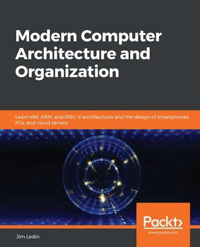
The following diagram shows the RISC-V base ISA regster set:
Figure 11.1: RISC-V base ISA register set
The registers are 32 bits wide. General-purpose registers x1 through x31 are available for use without any restrictions or special functions assigned by the processor hardware. The x0 register is hardwired to return zero when it is read, and will discard any value written to it. We will see some interesting uses of the x0 register shortly.
Each register has one or two alternate names, shown in Figure 11.1. These names correspond to the usage of registers in the standard RISC-V application binary interface (ABI). Because registers x1-x31 are functionally interchangeable, it is necessary for the ABI to dictate which register should serve as the stack pointer, which registers should contain arguments to functions, which should contain return values, and so forth. The meanings of the register designations are as follows:
- ra: Function return address.
- sp: Stack pointer.
- gp: Global data pointer.
- tp: Thread-local data pointer.
- t0-t6: Temporary storage.
- fp: Frame pointer for function-local stack data (this usage is optional).
- s0-s11: Saved registers (if the frame pointer is not in use, x8 becomes s0).
- a0-a7: Arguments passed to functions. Any additional arguments are passed on the stack. Function return values are passed in a0 and a1.
The pc register contains the 32-bit program counter, holding the address of the current instruction.
You may be surprised to see there is no processor flags register in the RISC-V ISA. Some operations that modify flags in other processor architectures instead store their results in a RISC-V register. For example, the signed (slt) and unsigned (sltu) RISC-V comparison instructions subtract two operands and set a destination register to 0 or 1 depending on the sign of the result. A subsequent conditional branch instruction can use the value in that register to determine which code path to take.
Some of the flags found in other processors must be computed in RISC-V. For example, there is no carry flag. To determine whether an addition resulted in a carry, it is necessary to perform a comparison between the sum and one of the operands of the addition instruction. If the sum is greater than or equal to the addend (either addend can be used for the comparison), a carry did not occur; otherwise, the addition produced a carry.
Most of the base ISA computational instructions use a three-operand format, in which the first operand is a destination register, the second operand is a source register, and the third operand is either a source register or an immediate value. The following is an example three-operand instruction:
add x1, x2, x3
This instruction adds the x2 register to the x3 register and stores the result in the x1 register.
To avoid introducing instructions that are not strictly necessary, many instructions take on extra duties that are performed by dedicated instructions in other processor architectures. For example, RISC-V contains no instruction that simply moves one register to another. Instead, a RISC-V addition instruction adds a source register and an immediate value of zero and stores the result in a destination register, producing the same result. The instruction to transfer the x2 register to the x1 register is therefore add x1, x2, 0, assigning the value (x2 + 0) to x1.
The RISC-V assembly language provides a number of pseudo-instructions using terminology that may be more familiar to implement such functions. The assembler translates the mv x1, x2 pseudo-instruction to a literal add x1, x2, 0 instruction.
The RISC-V base instruction set
The RISC-V base instruction set is composed of just 47 instructions. Eight are system instructions that perform system calls and access performance counters. The remaining 39 instructions fall into the categories of computational instructions, control flow instructions, and memory access instructions. We will examine each of these categories in the following sections.
Computational instructions
All of the computational instructions except lui and auipc use the three-operand form. The first operand is the destination register, the second is a source register, and the third operand is either a second source register or an immediate value. Instruction mnemonics using an immediate value (except for auipc) end with the letter i. This is a list of the instructions and their functions:
- add, addi, sub: Perform addition and subtraction. The immediate value in the addi instruction is a 12-bit signed value. The sub instruction subtracts the second source operand from the first. There is no subi instruction because addi can add a negative immediate value.
- sll, slli, srl, srli, sra, srai: Perform logical left and right shifts (sll and srl), and arithmetic right shifts (sra). Logical shifts insert zero bits into vacated locations. Arithmetic right shifts replicate the sign bit into vacated locations. The number of bit positions to shift is taken from the lowest 5 bits of the second source register or from the 5-bit immediate value.
- and, andi, or, ori, xor, xori: Perform the indicated bitwise operation on the two source operands. Immediate operands are 12 bits.
- slt, slti, sltu, sltui: The set if less than instructions set the destination register to 1 if the first source operand is less than the second source operand. This comparison is in terms of two's complement (slt) or unsigned (sltu) operands. Immediate operand values are 12 bits.
- lui: Load upper immediate. This instruction loads bits 12-31 of the destination register with a 20-bit immediate value. Setting a register to an arbitrary 32-bit immediate value requires two instructions. First, lui sets bits 12-31 to the upper 20 bits of the value. Then, addi adds in the lower 12 bits to form the complete 32-bit result. lui has two operands: the destination register and the immediate value.
- auipc: Add upper immediate to PC. This instruction adds a 20-bit immediate value to the upper 20 bits of the program counter. This instruction enables PC-relative addressing in RISC-V. To form a complete 32-bit PC-relative address, auipc forms a partial result, then an addi instruction adds in the lower 12 bits.
Control flow instructions
The conditional branching instructions perform comparisons between two registers and, based on the result, may transfer control within the range of a signed 12-bit address offset from the current PC. Two unconditional jump instructions are available, one of which (jalr) provides access to the entire 32-bit address range.
- beq, bne, blt, bltu, bge, bgeu: Branch if equal (beq), not equal (bne), less than (blt), less than unsigned (bltu), greater or equal (bge), or greater or equal, unsigned (bgeu). These instructions perform the designated comparison between two registers and, if the condition is satisfied, transfer control to the address offset provided in the 12-bit signed immediate value.
- jal: Jump and link. Transfer control to the PC-relative address provided in the 20-bit signed immediate value and store the address of the next instruction (the return address) in the destination register.
- jalr: Jump and link, register. Compute the target address as the sum of the source register and a signed 12-bit immediate value, then jump to that address and store the address of the next instruction in the destination register. When preceded by the auipc instruction, the jalr instruction can perform a PC-relative jump anywhere in the 32-bit address space.
Memory access instructions
The memory access instructions transfer data between a register and a memory location. The first operand is the register to be loaded or stored. The second operand is a register containing a memory address. A signed 12-bit immediate value is added to the address in the register to produce the final address used for the load or store.
The load instructions perform sign extension for signed values or zero extension for unsigned values. The sign or zero extension operation fills in all 32 bits in the destination register when a smaller data value (a byte or halfword) is loaded. Unsigned loads are specified by a trailing u in the mnemonic.
- lb, lbu, lh, lhu, lw: Load an 8-bit byte (lb), a 16-bit halfword (lh), or a 32-bit word (lw) into the destination register. For byte and halfword loads, the instruction will either sign-extend (lb and lh) or zero-extend (lbu and lhu) to fill the 32-bit destination register. For example, the lw x1, 16(x2) instruction loads the word at the address (x2 + 16) into register x1.
- sb, sh, sw: Store a byte (sb), halfword (sh), or word (sw) to a memory location matching the size of the data value.
- fence: Enforce memory access ordering in a multithreaded context. The purpose of this instruction is to ensure a coherent view of cached data across threads. This instruction takes two operands. The first specifies the types of memory accesses that must complete prior to the fence instruction. The second specifies the types of memory accesses controlled following the fence. The operation types ordered by this instruction are memory reads and writes (r and w) and I/O device inputs and outputs (i and o). For example, the fence rw, rw instruction will guarantee that all loads and stores involving memory addresses occurring before the fence instruction will complete before any subsequent memory loads or stores take place. This instruction ensures that any values present in processor caches are properly synchronized with memory or the I/O device.
- fence.i: This instruction ensures that any stores to instruction memory have completed before the fence.i instruction completes. This instruction is primarily useful in the context of self-modifying code.
System instructions
Of the eight system instructions, one invokes a system call, one initiates a debugger breakpoint, and the remaining six read and write system control and status registers (CSRs). The CSR manipulation instructions read the current value of the selected CSR into a register, then update the CSR by either writing a new value, clearing selected bits, or setting selected bits. The source value for the CSR modification is provided in a register or as an immediate 5-bit value. CSRs are identified by a 12-bit address. Each CSR instruction performs the read and write of the CSR as an atomic operation.
- ecall: Invoke a system call. Registers used for passing parameters into and returning from the call are defined by the ABI, not by processor hardware.
- ebreak: Initiate a debugger breakpoint.
- csrrw, csrrwi, csrrc, csrrci, csrrs, csrrsi: Read the specified CSR into a destination register and either write a source operand value to the register (csrrw), clear any 1 bit in the source operand in the register (csrrc), or set any 1 bit in the source operand in the register (csrrs). These instructions take three operands: the first is the destination register receiving the value read from the CSR, the second is the CSR address, and the third is a source register or a 5-bit immediate value (i suffix).
Six CSRs are defined in the base RISC-V architecture, all read-only. To execute any of the CSR access instructions in a read-only mode, the x0 register must be provided as the third operand. These registers define three 64-bit performance counters:
- cycle, cycleh: The lower (cycle) and upper (cycleh) 32 bits of the 64-bit count of elapsed system clock cycles since a reference time—typically, system startup. The frequency of the system clock may vary if dynamic voltage and frequency scaling (DVFS) is active.
- time, timeh: These are the lower (time) and upper (timeh) 32 bits of the 64-bit count of elapsed real-time clock cycles since a reference time—typically, system startup.
- instret, instreth: The lower (instret) and upper (instreth) 32 bits of the 64-bit count of processor instructions retired.
The two 32-bit halves of each performance counter cannot be read in a single atomic operation. To prevent erroneous readings, the following procedure should be used to reliably read each of the 64-bit counters:
- Read the upper 32 bits of the counter into a register.
- Read the lower 32 bits of the counter into another register.
- Read the upper 32 bits into yet another register.
- Compare the first and second reads of the upper 32 counter bits. If they differ, jump back to Step 1.
This procedure will read a valid count value, even though the counter continues to run between the reads. In general, execution of this sequence should require, at most, one backward jump in Step 4.
Pseudo-instructions
The RISC-V architecture has a truly reduced instruction set, lacking several types of instructions present in the instruction sets we have investigated in earlier chapters. The functions of many of those more familiar instructions can be performed with RISC-V instructions, though perhaps not in an immediately intuitive manner.
The RISC-V assembler supports a number of pseudo-instructions, each of which translates to one or more RISC-V instructions providing a type of functionality one might expect in a general-purpose processor instruction set. The following table presents a few of the most useful RISC-V pseudo-instructions:
Table 11.1: RISC-V pseudo-instructions

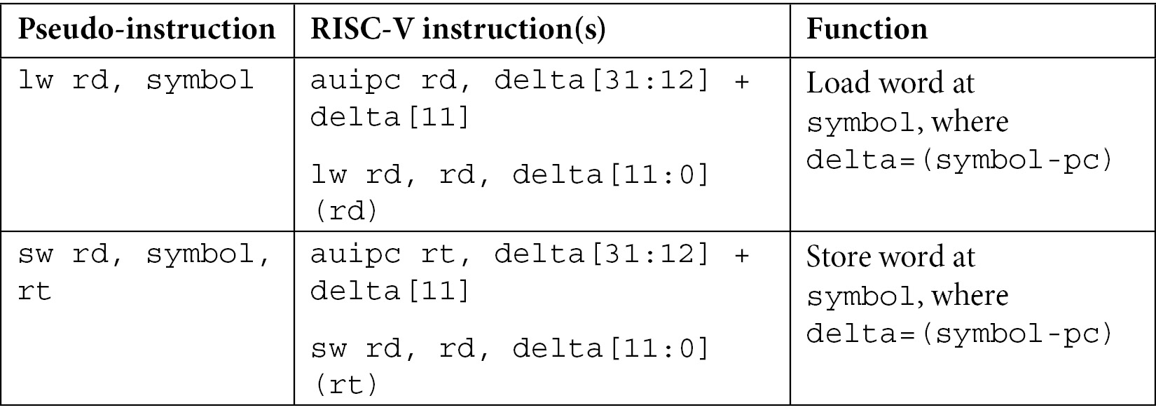
In these instruction listings, rd is the destination register, rs is the source register, csr is a control and status register, symbol is an absolute data address, and offset is a PC-relative instruction address.
Instructions combining the upper 20 bits of an address or immediate value with an immediate value containing the lower 12 bits must perform a step to reverse the effect of the sign extension of bit 11 of the lower 12-bit value in the second instruction of each sequence. This is necessary because the immediate value in the addi instruction is always treated as signed. The most significant bit of the 12-bit immediate value will be sign-extended through bit 31 before being added to the upper 20 bits.
The following example demonstrates the problem and the solution. Assume we want to load the value 0xFFFFFFFF into a register using lui and addi and naively add the upper and lower portions, as shown here
lui x1, 0xFFFFF # x1 now equals 0xFFFFF000
addi x1, x1, 0xFFF
The addi instruction sign-extends 0xFFF to 0xFFFFFFFF before adding it to 0xFFFFF000. The result of the addition is then 0xFFFFEFFF, which is not what we want. Adding bit 11 of the lower 12 bits to the upper 20 bits will fix this, as shown in the following code block:
lui x1, 0xFFFFF+1 # Add bit 11; x1 now equals 0x00000000
addi x1, x1, 0xFFF
The result is now 0xFFFFFFFF, the correct value. This procedure will work for any other numeric value. If bit 11 happens to be zero, nothing will be added to the upper 20 bits.
One point to note regarding assembly code in this chapter is that the RISC-V assembler uses the # character to begin a comment.
Privilege levels
The RISC-V architecture defines three privilege levels at which a thread can run:
- User (U) privilege level
- Supervisor (S) privilege level
- Machine (M) privilege level
All RISC-V implementations must support M mode, the most privileged level, which is capable of accessing all system features. M mode is entered at system reset. The code in a simple embedded system can run entirely in M mode.
In a slightly more sophisticated use case, a secure boot process might run at the M privilege level, loading and starting an application that runs in U mode. This approach is appropriate for a secure embedded solution.
In addition to the mandatory M level, a RISC-V processor may implement either or both of the S and U privilege levels. A system running a general-purpose operating system uses S mode and U mode in the same manner as the kernel and user modes of the processors and operating systems discussed in previous chapters. RISC-V U-mode applications request system services with the ecall (environment call) instruction, generating an exception handled at the S level. The privilege architecture of RISC-V directly supports modern operating systems such as Linux.
Separate collections of CSRs are defined to enable configuration, control, and monitoring of the system at each of the three privilege levels. Depending on the privilege level of the running thread and the level of a CSR, the thread may have read-write, read-only, or no access to the CSR. Threads at higher privilege levels can access CSRs at lower privilege levels.
The RISC-V S privilege level supports paged virtual memory with a 32-bit address space divided into 4 KB pages. A 32-bit virtual address is separated into a 20-bit virtual page number and a 12-bit page offset. Two additional virtual memory configurations are defined for the RISC-V 64-bit environment. The first is a 39-bit address space, supporting 512 GB of virtual memory. For applications requiring even more virtual addresses, a 48-bit address space is available, supporting 256 TB of virtual memory. Although the 48-bit configuration offers far more memory than the 39-bit configuration, it also requires additional storage for page tables, and consumes more processing time during traversal of those tables.
The following instructions support privileged execution levels:
- mret, sret, uret: These instructions return from the exception handler initiated by an ecall instruction. Each of these instructions can be executed at the privilege level indicated by the first letter of the instruction or higher. Executing one of these instructions referencing a privilege level lower than that of the current thread will return from the exception initiated at the lower level.
- wfi: Wait for interrupt. This instruction requests the current thread to stall until an interrupt becomes available for servicing. The RISC-V specification only requires that this instruction serve as a hint, so a particular implementation may process a wfi instruction as a no-op rather than actually stalling the thread. Because it is possible for the processor to handle wfi as a no-op, the code that follows a wfi instruction must explicitly check for the presence of pending interrupts in need of processing. This sequence typically occurs inside a loop.
- sfence.vma: Flush virtual memory page table data from cache to memory. The leading s in the instruction mnemonic indicates this instruction is targeted for use at the supervisor privilege level.
RISC-V defines additional instructions and CSRs supporting virtualization and the hypervisor that manages the virtual environment. RISC-V virtualization will be covered in Chapter 12, Processor Virtualization.
RISC-V extensions
The instruction set described earlier in this chapter is named RV32I, which stands for the RISC-V 32-bit integer instruction set. Although the RV32I ISA provides a complete and useful instruction set for many purposes, it lacks several functions and features available in other processors such as x86 and ARM.
The RISC-V extensions provide a mechanism for adding capabilities to the base instruction set in an incremental and compatible manner. Implementors of RISC-V processors can selectively include extensions in a processor design to optimize tradeoffs between chip size, system capability, and performance. These flexible design options are also available to developers of low-cost FPGA-based systems. We'll see more about implementing a RISC-V processor in an FPGA later in this chapter. The major extensions we will cover now are named M, A, C, F, and D, and we'll mention some other available extensions.
The M extension
The RISC-V M extension adds integer multiplication and division functionality to the base RV32I instruction set. The following instructions are available in this extension:
- mul: Multiply two 32-bit registers and store the lower 32 bits of the result in the destination register.
- mulh. mulhu, mulhsu: Multiply two 32-bit registers and store the upper 32 bits of the result in the destination register. Treat the multiplicands as both signed (mulh), both unsigned (mulhu), or signed rs1 times unsigned rs2 (mulhsu). rs1 is the first source register in the instruction and rs2 is the second.
- div, divu: Perform division of two 32-bit registers, rounding the result toward zero, on signed (div) or unsigned (divu) operands.
- rem, remu: Return the remainder corresponding to the result of a div or divu instruction on the operands.
Division by zero does not raise an exception. To detect division by zero, code should test the divisor and branch to an appropriate handler if it is zero.
The A extension
The RISC-V A extension provides atomic read-modify-write operations to support multithreaded processing in shared memory.
The atomic load-reserved (lr.w) and store-conditional (sc.w) instructions work together to perform a memory read followed by a write to the same location as an atomic sequence. The load-reserved instruction places a reservation on the memory address during the load. If another thread writes to the same location while the reservation is in effect, the reservation is canceled.
When the store-conditional instruction executes, it returns a value indicating whether it successfully completed the atomic operation. If the reservation remains valid (in other words, no intervening write occurred to the target address), the store-conditional instruction writes the register to memory and returns zero, indicating success. If the reservation was canceled, the store-conditional instruction does not alter the memory location and returns a nonzero value indicating the store operation failed. The following instructions implement the load-reserved and store-conditional operations:
- lr.w: Load a register from a memory location and place a reservation on the address.
- sc.w: Store a register to a memory location conditionally. Set the destination register to zero if the operation succeeded and the memory location was written, or set the destination register to a nonzero value if the reservation was canceled. If the reservation was canceled, the memory location is not modified by this instruction.
The atomic memory operation (AMO) instructions atomically load a word from a memory location into the destination register, perform a binary operation between the value that was loaded and rs2, and store the result back to the memory address. The following instructions implement the AMO operations:
- amoswap.w: Atomically swap rs2 into the rs1 memory location.
- amoadd.w: Atomically add rs2 into the rs1 memory location.
- amoand.w , amoor.w, amoxor.w: Atomically perform AND, OR, or XOR operations with rs2 into the rs1 memory location.
- amomin.w , amominu.w, amomax.w, amomaxu.w: Atomically perform minimum or maximum selection of signed or unsigned (instructions with the u suffix) values with rs2 into the rs1 memory location.
C extension
The RISC-V C extension implements compressed instructions with the goals of minimizing the amount of memory consumed by instruction storage and reducing the amount of bus traffic required to fetch instructions.
All RV32I instructions discussed previously are 32 bits in length. The C extension provides alternate 16-bit representations of many of the most frequently used RV32I instructions. Each compressed instruction is equivalent to one full-length instruction. No mode switching is necessary, meaning programs can freely intermix 32-bit RV32I instructions and compressed 16-bit instructions. In fact, assembly language programmers do not even need to take steps to specify whether an instruction should be generated in compressed form. The assembler and linker are capable of transparently emitting compressed instructions where possible to minimize code size, with no execution performance penalty.
When working with processors and software development tool sets supporting the RISC-V C extension, the benefits of compressed instructions are immediately available to developers working in assembly language as well as to those working with higher-level languages.
The F and D extensions
The RISC-V F and D extensions provide hardware support for single-precision (F) and double-precision (D) floating-point arithmetic in accordance with the IEEE 754 standard. The F extension adds 32 floating-point registers named f0-f31 and a control and status register named fcsr to the architecture. These registers are all 32 bits. The extension includes a set of floating-point instructions that complies with the IEEE 754-2008 single-precision standard.
Most floating-point instructions operate on the floating-point registers. Data transfer instructions are provided to load floating-point registers from memory, store floating-point registers to memory, and move data between floating-point registers and integer registers.
The D extension widens f0-f31 to 64 bits. In this configuration, each f register can hold a 32-bit value or a 64-bit value. Double-precision floating-point instructions are added, in compliance with the IEEE 754-2008 double-precision standard. The D extension requires the F extension be present.
Other extensions
Several additional extensions to the RISC-V architecture, detailed in the following list, have been defined, are in development, or are at least under consideration for future development:
- RV32E architecture: This is not actually an extension; rather, it is a modified architecture intended to reduce processor hardware requirements below those of the RV32I instruction set for the smallest embedded systems. The only difference between RV32I and RV32E is the reduction in the number of integer registers to 15. This change is expected to reduce processor die area and power consumption by about 25% compared to an otherwise equivalent RV23I processor. x0 remains a dedicated zero register. Halving the number of registers frees up 1 bit in each register specifier in an instruction. These bits are guaranteed to remain unused in future revisions and are thus available for use in customized instruction extensions.
- Q extension: The Q extension supports 128-bit quad-precision floating-point mathematics, as defined in the IEEE 754-2008 standard.
- L extension: The L extension supports decimal floating-point arithmetic, as defined in the IEEE 754-2008 standard.
- B extension: The B extension supports bit manipulations such as inserting, extracting, and testing individual bits.
- J extension: The J extension supports dynamically translated languages such as Java and JavaScript.
- T extension: The T extension supports memory transactions consisting of atomic operations across multiple addresses.
- P extension: The P extension provides packed Single Instruction Multiple Data (SIMD) instructions for floating-point operations in small RISC-V systems.
- V extension: The V extension supports data-parallel, or vector, operations. The V extension does not specify the lengths of data vectors; that decision is left to the implementers of a RISC-V processor design. A typical implementation of the V extension might support 512-bit data vectors, though implementations with up to 4,096-bit vector lengths are currently available.
- N extension: The N extension provides support for handling interrupts and exceptions at the U privilege level.
- Zicsr extension: The Zicsr extension performs atomic read-modify-write operations on the system CSRs. These instructions are described earlier in this chapter in the System instructions section.
- Zifencei extension: The Zifencei extension defines the fence.i instruction, described in the Memory access instructions section.
The next section covers the extension of the base RISC-V ISA to 64 bits.
64-bit RISC-V
The RISC-V introduction to this point has discussed the 32-bit RV32I architecture and instruction set, with extensions. The RV64I instruction set extends RV32I to a 64-bit architecture. As in RV32I, instructions are 32-bits wide. In fact, the RV64I instruction set is almost entirely the same as RV32I, except for these significant differences:
- All of the integer registers are widened to 64 bits.
- Addresses are widened to 64 bits.
- Bit shift counts in instruction opcodes increase in size from 5 to 6 bits.
- Several new instructions are defined to operate on 32-bit values in a manner equivalent to RV32I. These instructions are necessary because most instructions in RV64I operate on 64-bit values, and there are many situations in which it is necessary to operate efficiently on 32-bit values. These word-oriented instructions have an opcode mnemonic suffix of W. The W-suffix instructions produce signed 32-bit results. These 32-bit values are sign-extended (even if they are unsigned values) to fill the 64-bit destination register. In other words, bit 31 of each result is copied into bits 32-63.
The following new instructions are defined in RV64I:
- addw, addiw, subw, sllw, slliw, srlw, srliw, sraw, sraiw: These instructions perform equivalently to the RV32I instruction with the same mnemonic, minus the W suffix. They work with 32-bit operands and produce 32-bit results. The result is sign-extended to 64 bits.
- ld, sd: Load and store a 64-bit doubleword. These are the 64-bit versions of the lw and sw instructions in the RV32I instruction set.
The remaining RV32I instructions perform the same functions in RV64I, except addresses and registers are 64 bits in length. The same opcodes, both in assembly source code and binary machine code, are used in both instruction sets.
In the next section, we will examine some standard 32-bit and 64-bit RISC-V configurations that are commercially available. Each of these consists of a base ISA plus selected extensions.
Standard RISC-V configurations
The RV32I and RV64I instruction sets provide a base set of capabilities useful mainly in smaller embedded system designs. Systems intended to support multithreading, multiple privilege levels, and general-purpose operating systems require several of the RISC-V extensions to operate correctly and efficiently.
The minimum RISC-V configuration recommended for establishing an application development target consists of a base RV32I or RV64I instruction set architecture augmented with the I, M, A, F, D, Zicsr, and Zifencei extensions. The abbreviation for this combination of features is G, as in RV32G or RV64G. Many G configurations additionally support the compressed instruction extension, with the names RV32GC and RV64GC.
In embedded applications, a common configuration is RV32IMAC, providing the base instruction set plus multiply/divide functionality, atomic operations, and compressed instruction support. Marketing materials for RISC-V processors frequently use these shorthand descriptions of processor capabilities.
The following section presents a complete program in RISC-V assembly language.
RISC-V assembly language
The following RISC-V assembly language example is a complete application that runs on a RISC-V processor:
.section .text
.global main
main:
# Reserve stack space and save the return address
addi sp, sp, -16
sd ra, 0(sp)
# Print the message using the C library puts function
1: auipc a0, %pcrel_hi(msg)
addi a0, a0, %pcrel_lo(1b)
jal ra, puts
# Restore the return address and sp, and return to caller
ld ra, 0(sp)
addi sp, sp, 16
jalr zero, ra, 0
.section .rodata
msg:
.asciz "Hello, Computer Architect! "
This program prints the following message in a console window and then exits:
Hello, Computer Architect!
The following are some points of interest within the assembly code:
- The %pcrel_hi and %pcrel_lo directives select the high 20 bits (%pcrel_hi) or low 12 bits (%pcrel_lo) of the PC-relative address of the label provided as an argument. The combination of the auipc and addi instructions places the address of the message string in a0.
- 1: is a local label. When referencing a local label, the letter b is appended to reference a label earlier in the code (backward), or f is appended to reference a label later in the code (forward). The %pcrel_hi and %pcrel_lo directives are paired: the 1: local label resolves the lower 12 bits of the offset to the msg address.
In the next section, we will run some code in a fully functional RISC-V processor implemented in an FPGA.
Implementing RISC-V in an FPGA
All of the source code, processor hardware design intellectual property, and development tools required to build and implement a complete RISC-V processor in a low-cost FPGA are freely available on the Internet. This section provides a high-level overview of the open source RISC-V design and the steps for bringing it up in an FPGA device. The total cost for the hardware to accomplish this task is less than US$200.
The RISC-V FPGA target in this example is the Digilent Arty A7-35T board, available at https://store.digilentinc.com/arty-a7-artix-7-fpga-development-board-for-makers-and-hobbyists/. The Arty A7-35T costs US$129 at the time of this writing.
The Arty A7-35T contains a Xilinx Artix-7 XC7A35TICSG324-1L FPGA, which can be programmed to implement a RISC-V processor. The XC7A35TICSG324-1L has the following features:
- 5,200 logic slices.
- 1,600 of the logic slices can implement a 64-bit RAM.
- 41,600 flip-flops. Each logic slice contains eight flip-flops.
- 90 DSP slices supporting high-performance DSP MAC operations.
- 400 kbits of distributed RAM.
- 1,800 kbits of total RAM.
The Artix-7 FPGA architecture uses lookup tables (LUTs) to implement combinational logic. Each of the Artix-7 LUTs has six input signals and one output signal, where each signal is one data bit. A single LUT can represent any feedback-free circuit composed of AND, OR, NOT, and XOR gates operating on the six input signals by simply storing the results of each input combination as a bit in a small ROM. With 6 input bits, the ROM contains 64 (26) bits of data addressed by the six input signals. If desired, each LUT can instead be configured as two 32-bit LUTs operating on five shared inputs with 2 output bits. Optionally, the LUT output can be stored in a flip-flop.
A logic slice contains four LUTs and eight flip-flops, plus additional multiplexer and arithmetic carry logic. Four of the eight flip-flops in a slice can be configured as latches. Each of the 1,600 slices with 64-bit RAM capability can alternatively implement a 32-bit shift register or two 16-bit shift registers.
The low-level LUTs and other facilities provided by the several thousand logic slices represent the raw materials needed to assemble a complete RISC-V processor plus peripheral devices within a single FPGA. The FPGA programming process interconnects components within the FPGA to form a complex digital device defined in a hardware definition language.
From the perspective of the system designer, it is not necessary to understand the detailed inner workings of the Xilinx FPGA. The designer works at the hardware design language level. A tool such as Vivado, introduced in the solutions to the exercises in Chapter 2, Digital Logic, translates the hardware design language (typically, VHDL or Verilog, though the RISC-V design is implemented in the Chisel and Scala languages) into a compiled format suitable for programming an FPGA device.
The designer's primary concerns in regard to the FPGA are that the system design is capable of fitting within the resource constraints of the FPGA device and that the resulting implementation operates with acceptable efficiency. In this example, the XC7A35TICSG324-1L FPGA provides more than enough resources to implement the RISC-V processor efficiently.
To develop and run programs on the Arty A7-35T RISC-V processor, you also need a low-cost hardware debugger. The Olimex ARM-TINY-USB-H debugger is available for US$45.67 at https://www.digikey.com/product-detail/en/olimex-ltd/ARM-USB-TINY-H/1188-1013-ND/3471388. You will also need some jumper wires to connect the debugger to the Arty A7-35T board. These are available for US$3.95 at https://www.adafruit.com/product/826. Finally, the Arty A7-35T processor requires a Universal Serial Bus (USB) cable to connect its USB Micro-B connector to your host computer system. Other than your host computer system, no additional hardware is required. All of the software and design data required to implement the RISC-V in Arty is available for free download from the Internet.
The processor we will implement in the Arty A7-35T is the Freedom E310 Arty, an open source implementation of an RV32IMAC core with support for interrupt processing. Peripheral devices include 16 general-purpose I/O (GPIO) signals and a serial port.
The Freedom E310 processor is provided as source code, and is therefore modifiable by users who wish to implement customized versions of the processor. The hardware design languages used in the RISC-V processor hardware code are Chisel and Scala.
Chisel is a domain-specific language targeted to the development of complex digital hardware devices such as SoCs. Chisel runs on top of Scala, a modern, general-purpose programming language supporting the functional and object-oriented programming paradigms. Scala is a pure object-oriented language in which every value is an object. It is also a functional language in the sense that every function is a value. Scala compiles to Java bytecode and runs on the standard Java Virtual Machine. Scala programs can directly use any of the thousands of available Java libraries.
RISC-V support for customized extensions
The RISC-V architecture explicitly supports customized variations in the form of custom opcodes, coprocessors, and other modifications, so long as they are compatible with the RISC-V customization rules. Starting from the open source RISC-V design, you can implement custom modifications that will be guaranteed to remain compatible with future versions of RISC-V standards and extensions.
Chisel and Scala are preferred in the design of complex digital systems today because of the higher-level nature of these languages compared to traditional hardware design languages such as VHDL and Verilog. While it's true that any circuit you might design in Chisel can also be designed in VHDL, there are some substantial benefits to using Chisel. For example, the compilation process transforms the Chisel/Scala code into a form called Flexible Intermediate Representation for RTL (FIRRTL), where RTL stands for register-transfer level, which is the abstraction level used in synchronous circuit hardware design languages such as VHDL. Using freely available tools, it is possible to perform optimizations on the FIRRTL representation of a circuit that result in a better-performing FPGA implementation than a comparable design in VHDL or Verilog would be likely to provide.
One way to appreciate the difference between Chisel and VHDL/Verilog is the analogous differentiation between the Python and C programming languages. While you can implement the functional equivalent of any Python program in C, Python programs can express far more high-level functionality in a few lines of code than a similar size program in C.
We can compare Chisel code to the VHDL example we looked at in the Hardware description languages section of Chapter 2, Digital Logic. Consider the VHDL version of the single-bit full adder presented in that chapter, shown in the following code block:
-- Load the standard libraries
library IEEE;
use IEEE.STD_LOGIC_1164.ALL;
-- Define the full adder inputs and outputs
entity FULL_ADDER is
port (
A : in std_logic;
B : in std_logic;
C_IN : in std_logic;
S : out std_logic;
C_OUT : out std_logic
);
end entity FULL_ADDER;
-- Define the behavior of the full adder
architecture BEHAVIORAL of FULL_ADDER is
begin
S <= (A XOR B) XOR C_IN;
C_OUT <= (A AND B) OR ((A XOR B) AND C_IN);
end architecture BEHAVIORAL;
The Chisel equivalent of the full adder is shown in the following code block:
import chisel3._
class FullAdder extends Module {
val io = IO(new Bundle {
val a = Input(UInt(1.W))
val b = Input(UInt(1.W))
val c_in = Input(UInt(1.W))
val s = Output(UInt(1.W))
val c_out = Output(UInt(1.W))
})
io.s := (io.a ^ io.b) ^ io.c_in
io.c_out := (io.a & io.b) | ((io.a ^ io.b) & io.c_in)
}
In this code, the IO bundle defines the module inputs and outputs. The argument to each Input and Output parameter defines the data type (Uint) and the bit width (1.W, indicating each input and output signal is 1 bit wide).
While this simple example does not demonstrate the full range of benefits of developing complex circuits in Chisel, it shows that, at the level of detailed implementation, it does not look too different from VHDL. We won't delve further into the details of Chisel here. For further information, consult the Chisel repository at https://github.com/freechipsproject/chisel3.
The process of building the RISC-V processor and programming it into the Arty A7-35T board consists of the following steps:
- Translate the Chisel and Scala code into the FIRRTL form.
- Translate the FIRRTL into Verilog.
- Compile the Verilog into an FPGA image.
- Program the FPGA image onto the Arty A7-35T board.
The detailed commands to perform each of these steps are presented in the answers to the exercises at the end of this chapter.
Once you have programmed the RISC-V image onto the Arty board, it will be possible to connect a software development suite to the board through the debugger interface. From this point, you can develop RISC-V code in assembly language or in high-level languages, compile it, and run it on the FPGA RISC-V processor in the same manner as with a hardware processor.
Summary
This chapter introduced the RISC-V processor architecture and its instruction set. The RISC-V project has defined a complete user-mode instruction set specification and a number of extensions to support general-purpose computing, high-performance computing, and embedded applications requiring minimal code size. RISC-V processors are offered commercially, and open source products are available to implement instantiations of RISC-V in FPGA devices.
Having completed this chapter, you should understand the architecture and features of the RISC-V processor and its optional extensions. You learned the basics of the RISC-V instruction set and now understand how RISC-V can be tailored to target a variety of application domains, from low-end micropower embedded systems to warehouse-scale cloud server farms. You also learned how to implement a RISC-V processor in a low-cost FPGA board.
The next chapter introduces the concept of processor virtualization, where rather than running code directly on a host processor, an entire virtual environment is implemented to run perhaps several virtual processors, each with its own operating system and applications, on a single physical processor.
Exercises
- Visit https://www.sifive.com/boards/ and download Freedom Studio. Freedom Studio is an Eclipse integrated development environment (IDE)-based development suite with a complete set of tools for building a RISC-V application and running it on a hardware RISC-V processor or in the emulation environment included with Freedom Studio. Follow the instructions in the Freedom Studio User Manual to complete the installation. Start Freedom Studio and create a new Freedom E SDK project. In the project creation dialog, select qemu-sifive-u54 as the target (this is a single-core 64-bit RISC-V processor in the RV64GC configuration). Select the hello example program and click the Finish button. This will start a build of the example program and the RISC-V emulator. After the build completes, the Edit Configuration dialog box will appear. Click Debug to start the program in the emulator debug environment. Single-step through the program and verify the text Hello, World! appears in the console window.
- With the project from Exercise 1 still open, locate the hello.c file in the src folder in the Project window. Right-click on the file and rename it hello.s. Open hello.s in the editor and delete the entire contents. Insert the assembly language program shown in the RISC-V assembly language section in this chapter. Perform a clean, and then rebuild the project (press Ctrl+ 9 to initiate the clean operation). Select Debug under the Run menu. Once the debugger starts, open windows to display the hello.s source file, the Disassembly window, and the Registers window. Expand the Registers tree to display the RISC-V processor registers. Single-step through the program and verify the text Hello, Computer Architect! appears in the console window.
- Write a RISC-V assembly language program that computes the following expression and prints the result as a hexadecimal number:
 . As part of this program, create a callable function to print 1 byte as two hex digits.
 - Program an Arty A7-35T board with a RISC-V processor image. Build and run the hello assembly language program shown in the RISC-V assembly language section in this chapter on the RISC-V processor using the Olimex ARM-TINY-USB-H debugger, as described in the Implementing RISC-V in an FPGA section near the end of this chapter. Verify the program outputs the text Hello, Computer Architect!.