Chapter 8: Performance-Enhancing Techniques
The fundamental aspects of processor and memory architectures discussed in previous chapters enable the design of a complete and functional computer system. However, the performance of such a system would be poor compared to most modern processors without the addition of features to increase the speed of instruction execution.
Several performance-enhancing techniques are employed routinely in processor and system designs to achieve peak execution speed in real-world computer systems. These techniques do not alter what the processor does in terms of program execution and data processing; they just help get it done faster.
After completing this chapter, you will understand the value of multilevel cache memory in computer architectures and the benefits and challenges associated with instruction pipelining. You'll also understand the performance improvement resulting from simultaneous multithreading and the purpose and applications of single instruction, multiple data processing.
The following topics will be covered in this chapter:
- Cache memory
- Instruction pipelining
- Simultaneous multithreading
- SIMD processing
Cache memory
A cache memory is a memory region that stores program instructions or data, usually instructions or data that have been accessed recently, for future use. The primary purpose of cache memory is to increase the speed of repeatedly accessing the same memory location or nearby memory locations. To be effective, accessing the cached data must be significantly faster than accessing the original source of the data, referred to as the backing store.
When caching is in use, each attempt to access a memory location begins with a search of the cache. If the data is present, the processor retrieves and uses it immediately. This is called a cache hit. If the cache search is unsuccessful (a cache miss), the data must be retrieved from the backing store. In the process of retrieving the requested data, a copy is added to the cache for anticipated future use.
Cache memory is used for a variety of purposes in computer systems. Some examples of cache memory applications are:
- Translation lookaside buffer (TLB): The TLB, as we saw in in Chapter 7, Processor and Memory Architectures, is a form of cache memory used in processors supporting paged virtual memory. The TLB contains a collection of virtual-to-physical address translations that speed access to page frames in physical memory. As instructions execute, each main memory access requires a virtual-to-physical translation. Successful searches of the TLB result in much faster instruction execution compared to the page table lookup process following a TLB miss. The TLB is part of the MMU, and is not directly related to the varieties of processor cache memory discussed later in this section.
- Disk drive caches: Reading and writing the magnetized platters of rotating disk drives is orders of magnitude slower than accessing DRAM devices. Disk drives generally implement cache memory to store the output of read operations and to temporarily hold data in preparation for writing. Drive controllers often read more data than the amount originally requested in internal cache memory in the expectation that future reads will request data adjacent to the initial request. If this turns out to be a correct assumption, which it often is, the drive will satisfy the second request immediately from cache without the delay associated with accessing the disk platters.
- Web browser caches: Web browsers generally store copies of recently accessed web pages in memory in the expectation that the user will sometimes click the "Back" button to return to a previously viewed page. When this happens, the browser can retrieve some or all of the page content from its local cache and immediately redisplay the page without the need to access the remote web server and retrieve the same information again.
- Processor instruction and data caches: The following sections examine processor cache structures in detail. The purpose of these caches is to improve the speed of access to instructions and data in comparison to the latency incurred when accessing DRAM modules.
Cache memory improves computer performance because many algorithms executed by operating systems and applications exhibit locality of reference. Locality of reference refers to the reuse of data that has been accessed recently (this is referred to as temporal locality) and to the access of data in physical proximity to data that has been accessed previously (called spatial locality).
Using the structure of the TLB as an example, temporal locality is exploited by storing a virtual-to-physical translation in the TLB for some period of time following initial access to a particular page frame. Any additional references to the same page frame in subsequent instructions will enjoy speedy access to the translation until it is eventually replaced in the cache by a different translation.
The TLB exploits spatial locality by referencing an entire page frame with a single TLB entry. Any subsequent accesses to different addresses on the same page will benefit from the presence of the TLB entry resulting from the first reference to the page.
As a general rule, cache memory regions are small in comparison to the backing store. Cache memory devices are designed for maximum speed, which generally means they are more complex and costly per bit than the data storage technology used in the backing store. As a consequence of their limited size, cache memory devices tend to fill quickly. When a cache does not have an available location to store a new entry, an older entry must be discarded. The cache controller uses a cache replacement policy to select which cache entry will be overwritten by the new entry.
The goal of processor cache memory is to maximize the percentage of cache hits over time, thus providing the highest sustained rate of instruction execution. To achieve this objective, the caching logic must determine which instructions and data will be placed into the cache and retained for future use.
In general, a processor's caching logic does not have any assurance that a cached data item will ever be used again once it has been inserted into the cache. The logic relies on the likelihood that, due to temporal and spatial locality, there is a very good chance the cached data will be accessed in the near future. In practical implementations on modern processors, cache hits typically occur on 95 to 97 percent of memory accesses. Because the latency of cache memory is a small fraction of the latency of DRAM, a high cache hit rate leads to a substantial performance improvement in comparison to a cache-less design.
The following sections discuss the multilevel caching technologies of modern processors and some of the cache replacement policies commonly used in their implementations.
Multilevel processor caches
In the years since the introduction of personal computers, processors have undergone dramatic increases in the speed of instruction processing. The internal clocks of modern Intel and AMD processors are close to 1,000 times faster than the 8088 processor used in the first IBM PC. The speed of DRAM technology, in comparison, has increased at a much slower rate over time. Given these two trends, if a modern processor were to access DRAM directly for all of its instructions and data, it would spend the vast majority of its time simply waiting for the DRAM to respond to each request.
To attach some approximate numbers to this topic, consider a modern processor capable of accessing a 32-bit data value from a processor register in 1 ns. Accessing the same value from DRAM might take 100 ns. Oversimplifying things somewhat, if each instruction requires a single access to a memory location, and the execution time for each instruction is dominated by the memory access time, we can expect a processing loop that accesses the data it requires from processor registers to run 100 times faster than the same algorithm accessing main memory on each instruction.
Now, assume a cache memory is added to the system with an access time of 4 ns. By taking advantage of cache memory, the algorithm that accesses DRAM on each instruction will suffer the 100 ns performance penalty the first time a particular address is referenced, but subsequent accesses to the same and nearby addresses will occur at the cache speed of 4 ns. Although accessing the cache is four times slower than accessing registers, it is 25 times faster than accessing DRAM. This example represents the degree of execution speedup achievable through the effective use of cache memory in modern processors.
High-performance processors generally employ multiple cache levels with the goal of achieving peak instruction execution rate. Processor cache hardware is constrained in terms of size and performance by the economics of semiconductor technology. Selecting an optimally performing mix of processor cache types and sizes while achieving a price point acceptable to end users is a key goal of processor designers.
The two types of RAM circuits in common use as main memory and for processor internal storage are dynamic RAM (DRAM) and static RAM. DRAM is inexpensive, but has a comparatively slow access time, due largely to the time required to charge and discharge the bit cell capacitors during read and write operations. Static RAM is much faster than DRAM, but is much more costly, resulting in its use in smaller quantities in applications where performance is critical. DRAM designs are optimized for density, resulting in the largest possible number of bits stored on a single DRAM integrated circuit. Static RAM designs are optimized for speed, minimizing the time to read or write a location. Processor cache memory is generally implemented using SRAM.
Static RAM
Static RAM (SRAM) boasts a substantially faster access time than DRAM, albeit at the expense of significantly more complex circuitry. SRAM bit cells take up much more space on the integrated circuit die than the cells of a DRAM device capable of storing an equivalent quantity of data. As you will recall from Chapter 4, Computer System Components, a single DRAM bit cell consists of just one MOSFET transistor and one capacitor.
The standard circuit for a single bit of SRAM contains six MOSFET transistors. Four of these transistors are used to form two NOT gates. These gates are based on the CMOS circuit shown in Figure 4.3 in Chapter 4, Computer System Components in the Digital switching circuits based on the MOSFETsection. These gates are labeled G1 and G2 in the following diagram:

Figure 8.1: SRAM circuit diagram
The output of each of the NOT gates is connected to the input of the other, forming a flip-flop. Most of the time, the wordline is low, which turns off transistor switches T1 and T2, isolating the pair of gates. While the wordline is low, as long as power is applied, the gates will persist on one of two states:
- The stored bit is 0: The input of G1 is low and its output is high.
- The stored bit is 1: The input of G1 is high and its output is low.
The access transistors (T1 and T2) function as switches that connect the bitlines to the cell for reading and writing. As with DRAM, driving the wordline high enables access to the bit cell by reducing the resistance across each access transistor to a very small value. To read the cell contents, the readout circuitry measures the voltage between the bitline pair labeled Bitline and Bitline where the overbar represents the NOT operation). The two bitline signals always have opposing senses, forming a differential pair. Measuring the sign of the voltage difference between the two signals determines whether the cell contains a 0 or a 1.
To write the bit cell, the wordline is driven high, and the and signals are driven to opposite voltage levels representing the desired value (0 or 1) to be written. The transistors writing the data to the bitlines must have substantially greater drive capability than the bit cell NOT gate transistors. This allows the desired value to be written to the cell, even if the flip-flop state must be overpowered to switch it to the state being written.
An SRAM bank is arranged in a rectangular grid of rows and columns in the same manner as DRAM. The wordline enables access to all SRAM bit cells along a single row. The bitlines connect to all columns of the grid of bit cells.
Note that, unlike DRAM, SRAM does not require periodic refreshes to retain its data content. This is why it is referred to as static RAM.
Level 1 cache
In a multilevel cache architecture, the cache levels are numbered, beginning with 1. A level 1 cache (also referred to as an L1 cache) is the first cache the processor searches when requesting an instruction or data item from memory. Because it is the first stop in the cache search, an L1 cache is generally constructed using the fastest SRAM technology available and is physically located as close to the processor's logic circuitry as possible. The emphasis on speed makes an L1 cache costly and power-hungry, which means it must be relatively small in size, particularly in cost-sensitive applications. Even when it is quite small, a fast level 1 cache can provide a substantial performance boost in comparison to an equivalent processor that does not employ caching.
The processor (or the MMU, if present) transfers data between DRAM and cache in fixed-size data blocks called cache lines. Computers using DDR DRAM modules generally use a cache line size of 64 bytes. The same cache line size is commonly used in all cache levels.
Modern processors often divide the L1 cache into two sections of equal size, one for instructions and one for data. This configuration is referred to as a split cache. In a split cache, the level 1 instruction cache is referred to as the L1 I-cache and the level 1 data cache is referred to as the L1 D-cache. The processor uses separate buses to access each of the two caches, thereby implementing a significant aspect of the Harvard architecture. This arrangement speeds instruction execution by enabling access to instructions and data in parallel, assuming L1 cache hits for both.
Modern processors employ a variety of strategies to organize cache memory and control its operation. The simplest cache configuration is direct mapping, introduced in the next section.
Direct-mapped cache
A direct-mapped cache is a block of memory organized as a one-dimensional array of cache sets, where each address in the main memory maps to a single set in the cache. Each cache set consists of the following items:
- A cache line, containing a block of data read from main memory
- A tag value, indicating the location in main memory corresponding to the cached data
- A valid bit, indicating whether the cache set contains data
There are times when the cache contains no data, such as immediately following processor power-on. The valid bit for each cache set is initially clear to indicate the absence of data in the set. When the valid bit is clear, use of the set for lookups is inhibited. Once data has been loaded into a cache set, the hardware sets the valid bit.
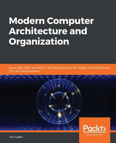
We will use a small L1 I-cache size of 512 bytes as an example. Because this is a read-only instruction cache, it need not support the ability to write to memory. The cache line size is 64 bytes. Dividing 512 bytes by 64 bytes per set results in 8 cache sets. The 64 bytes in each set equals 26 bytes, which means the least significant 6 bits in the address select a location within the cache line. Three additional bits of an address are required to select one of the eight sets in the cache.
From this information, the following diagram shows the division of a 32-bit physical memory address into tag, set number, and cache line byte offset components:

Figure 8.2: Components of a 32-bit physical memory address
Each time the processor reads an instruction from DRAM (which is necessary any time the instruction is not already present in the cache), the MMU reads the 64-byte block containing the addressed location, and stores it in the L1 I-cache set selected by the three Set bits of Figure 8.2. The upper 23 bits of the address are stored in the Tag field of the cache set, and the Valid bit is set, if it was not already set.
As the processor fetches each subsequent instruction, the control unit uses the three Set bits in the instruction's address to select a cache set for comparison. The hardware compares the upper 23 bits of the executing instruction's address with the Tag value stored in the selected cache set. If the values match, a cache hit has occurred, and the processor reads the instruction from the cache line. If a cache miss occurs, the MMU reads the line from DRAM into cache and provides the instruction to the control unit for execution.
The following diagram represents the organization of the entire 512-byte cache and its relation to the three fields in a 32-bit instruction address:
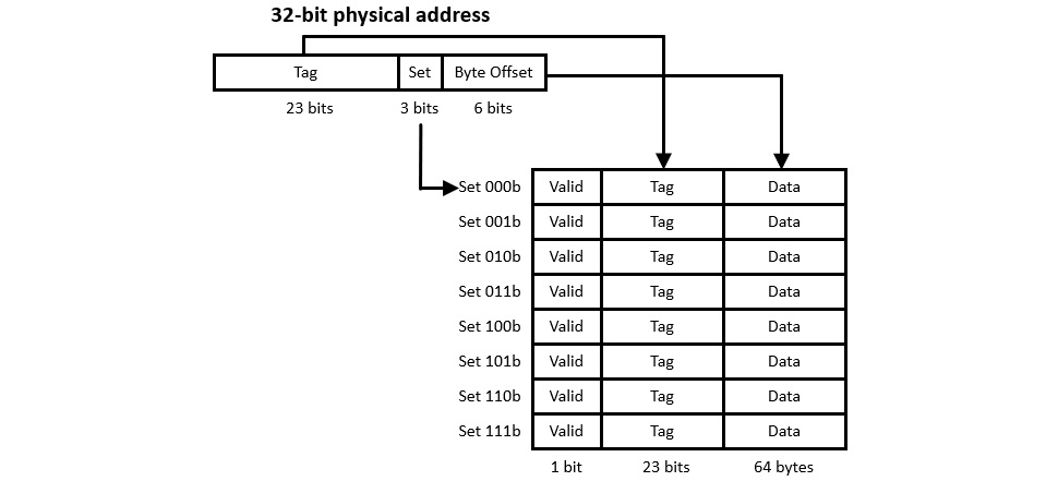
Figure 8.3: Relation of a 32-bit physical address to cache memory
To demonstrate why a direct-mapped cache can produce a high hit rate, assume we're running a program containing a loop starting at physical memory address 8000h (we're ignoring the upper 16 bits of the 32-bit address here for simplicity) and containing 256 bytes of code. The loop executes instructions sequentially from the beginning to the end of the 256 bytes, and then branches back to the top of the loop for the next iteration.
Address 8000h contains 000b in its Set field, so this address maps to the first cache set, as shown in Figure 8.3. On the first pass through the loop, the MMU retrieves the 64-byte Set 000b cache line from DRAM and stores it in the first set of the cache. As the remaining instructions stored in the same 64-byte block execute, each will be retrieved directly from cache. As execution flows into the second 64 bytes, another read from DRAM is required. By the time the end of the loop is reached, Sets 000b through 011b have been populated with the loop's 256 bytes of code. For the remaining passes through the loop, assuming the thread runs without interruption, the processor will achieve a 100 percent cache hit rate, and will achieve maximum instruction execution speed.
Alternatively, if the instructions in the loop happen to consume significantly more memory, the advantage of caching will be reduced. Assume the loop's instructions occupy 1,024 bytes, twice the cache size. The loop performs the same sequential execution flow from top to bottom. When the instruction addresses reach the midpoint of the loop, the cache has been completely filled with the first 512 bytes of instructions. At the beginning of the next cache line beyond the midpoint, the address will be 8000h plus 512, which is 8200h. 8200h has the same Set bits as 8000h, which causes the cache line for address 8000h to be overwritten by the cache line for address 8200h. Each subsequent cache line will be overwritten as the second half of the loop's code executes.
Even though all of the cached memory regions are overwritten on each pass through the loop, the caching structure continues to provide a substantial benefit because, once read from DRAM, each 64-byte line remains in the cache and is available for use as its instructions are executed. The downside in this example is the increased frequency of cache misses. This represents a substantial penalty because, as we've seen, accessing an instruction from DRAM may be 25 (or more) times slower than accessing the same instruction from the L1 I-cache.
Virtual and physical address tags in caching
The example in this section assumes that cache memory uses physical memory addresses to tag cache entries. This implies that the addresses used in cache searches are the output of the virtual-to-physical address translation process in systems using paged virtual memory. It is up to the processor designer to select whether to use virtual or physical addresses for caching purposes.
In modern processor caches, it is not uncommon to use virtual address tags in one or more cache levels and physical address tags in the remaining levels. One advantage of using virtual address tagging is speed, due to the fact that no virtual-to-physical translation is required during cache accesses. As we've seen, virtual-to-physical translation requires a TLB lookup and potentially a page table search in the event of a TLB miss. However, virtual address tagging introduces other issues such as aliasing, which occurs when the same virtual address refers to different physical addresses. As with many other aspects of processor performance optimization, this is a trade-off to be considered during cache system design.
This example was simplified by assuming instruction execution flows linearly from the top to the bottom of the loop without any detours. In real-world code, there are frequent calls to functions in different areas of the application memory space and to system-provided libraries. In addition to those factors, other system activities such as interrupt processing and thread context switching frequently overwrite information in the cache, leading to a higher cache miss frequency. Application performance is affected because the main-line code must perform additional DRAM accesses to reload the cache following each detour that causes a cache entry to be overwritten.
One way to reduce the effects of deviations from straight-line code execution is to set up two caches operating in parallel. This configuration is called a two-way set associative cache, discussed next.
Set associative cache
In a two-way set associative cache, the memory is divided into two equal-sized caches. Each of these has half the number of entries of a direct-mapped cache of the same total size. The hardware consults both of these caches in parallel on each memory access and a hit may occur in either one. The following diagram illustrates the simultaneous comparison of a 32-bit address tag against the tags contained in two L1 I-caches:
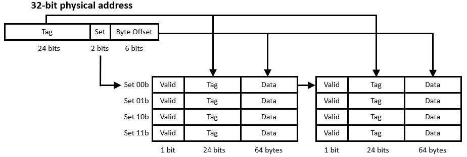
Figure 8.4: Set associative cache operation
The cache configuration shown here contains the same cache line size (64 bytes) as the cache in Figure 8.3, but only half as many sets per cache. The overall size of cache memory is the same as the previous example: 64 bytes per line times 4 rows times 2 caches equals 512 bytes. Because there are now four sets, the Set field in the physical address reduces to two bits and the Tag field increases to 24 bits. Each set consists of two cache lines, one in each of the two caches.
When a cache miss occurs, the memory management logic must select which of the two cache tables to use as the destination for the data being loaded from DRAM. A common method is to track which of the relevant sets in the two tables has gone the longest without being accessed, and overwrite that entry. This replacement policy, called least-recently used (LRU), requires hardware support to keep track of which cache line has been idle the longest. The LRU policy relies on the temporal locality heuristic stating that data that has not been accessed for an extended period of time is less likely to be accessed again in the near future.
Another method for selecting between the two tables is to simply alternate between them on successive cache insertions. The hardware to implement this replacement policy is simpler than the LRU policy, but there may be a performance impact due to the arbitrary selection of the line being invalidated. Cache replacement policy selection represents another area of trade-off between increased hardware complexity and incremental performance improvements.
In a two-way set associative cache, two cache lines from different physical locations with matching Set fields are present in cache simultaneously, assuming both cache lines are valid. At the same time, in comparison to a direct-mapped cache of the same total size, each of the two-way set associative caches is half the size. This represents yet another design tradeoff.
The number of unique Set values that can be stored in a two-way set associative cache is reduced compared to direct mapping, but multiple cache lines with identical Set fields can be cached simultaneously. The cache configuration that provides the best overall system performance will depend on the memory access patterns associated with the types of processing activity performed on the system.
Set associative caches can contain more than the two caches of this example. Modern processors often have four, eight, or 16 parallel caches, referred to as 4-way, 8-way, and 16-way set associative caches, respectively. These caches are referred to as set associative because an address Tag field associates with all of the cache lines in the set simultaneously. A direct-mapped cache implements a one-way set associative cache.
The advantage of multi-way set associative caches over direct-mapped caches is that they tend to have higher hit rates, thereby providing better system performance than direct-mapped caches in most practical applications. If multi-way set associative caches provide better performance than one-way direct mapping, why not increase the level of associativity even further? Taken to the limit, this progression ends with fully associative caching.
Fully associative cache
Assuming the number of lines in the cache is a power of two, repetitively dividing the overall cache memory into a larger number of smaller parallel caches, until each cache contains only one line, results in a fully associative cache. In our example of a 512 byte cache with 64 bytes per cache line, this process would result in eight parallel caches, each with only one set.
In this architecture, every memory access leads to a parallel comparison with the Tag values stored in all of the cache lines. A fully associative cache using an effective replacement policy such as LRU can provide a very high hit rate, though at a substantial cost in circuit complexity and a corresponding consumption of integrated circuit die area. In power-sensitive applications such as battery-powered mobile devices, the additional circuit complexity of a fully associative cache leads to increased battery drain. In desktop computers and cloud servers, excessive processor power consumption must be minimized to avoid the need for extraordinary cooling requirements and to minimize the electric utility bill for cloud providers operating thousands of servers. Because of these costs, fully associative caches are rarely used as instruction and data caches in modern processors.
The concept behind the fully associative cache may sound familiar because it is the same concept employed in the TLB presented in Chapter 7, Processor and Memory Architectures. The TLB is typically a fully associative cache containing virtual-to-physical address translations. Although the use of fully associative caching in the TLB results in the drawbacks of circuit complexity, die area consumption, and power consumption described in the preceding paragraph, the performance benefit provided by the TLB is so substantial that full associativity is used in virtually all high-performance processors that implement paged virtual memory.
Our discussion to this point has focused on instruction caching, which is normally a read-only process. The functional requirements for the data cache are similar to those of the instruction cache, with one significant extension: in addition to reading from data memory, the processor must be free to write to data memory.
Processor cache write policies
In processors with split caches, the L1 D-cache is similar in structure to the L1 I-cache, except that the circuitry must permit the processor to write to memory as well as read from it. Each time the processor writes a data value to memory, it must update the L1 D-cache line containing the data item, and, at some point, it must also update the DRAM location in physical memory containing the cache line. As with reading DRAM, writing to DRAM is a slow process compared to the speed of writing to the L1 D-cache.
The most common cache write policies in modern processors are as follows:
- Write-through: This policy updates DRAM immediately every time the processor writes data to memory.
- Write-back: This policy holds the modified data in the cache until the line is about to be evicted from cache. A write-back cache must provide an additional status bit associated with each cache line indicating whether the data has been modified since it was read from DRAM. This is called the dirty bit. If set, the dirty bit indicates that the data in that line is modified and the system must write the data to DRAM before its cache line can be freed for reuse.
The write-back policy generally results in better system performance because it allows the processor to perform multiple writes to the same cache line without the need to access main memory on each write. In systems with multiple cores or multiple processors, the use of write-back caching introduces complexity, because the L1 D-cache belonging to a core that writes to a memory location will contain data that differs from the corresponding DRAM location, and from any copies in the caches of the other processors or cores. This memory content disagreement will persist until the cache line has been written to DRAM and refreshed in any processor caches it occupies.
It is generally unacceptable to have different processor cores retrieve different values when accessing the same memory location, so a solution must be provided to ensure that all processors see the same data in memory at all times. The challenge of maintaining identical views of memory contents across multiple processors is called the cache coherence problem.
A multi-core processor can resolve this issue by sharing the same L1 D-cache among all the cores, but modern multi-core processors usually implement a separate L1 D-cache for each core to maximize access speed. In multiprocessor systems with shared main memory, where the processors are on separate integrated circuits, and in multi-core processors that do not share L1 cache, the problem is more complex.
Some multiprocessor designs perform snooping to maintain cache coherence. Each processor snoops by monitoring memory write operations performed by the other processors. When a write occurs to a memory location present in the snooping processor's cache, the snooper takes one of two actions: it can invalidate its cache line by setting the Valid bit to false, or it can update its cache line with the data written by the other processor. If the cache line is invalidated, the next access to the line's physical memory location will result in a DRAM access, which picks up the data modified by the other processor.
Snooping can be effective in systems with a limited number of processors, but it does not scale well to systems containing dozens or hundreds of processors, because each processor must monitor the write behavior of all the other processors at all times. Other, more sophisticated, cache coherence protocols must be implemented in systems with large numbers of processors.
Level 2 and level 3 processor caches
The discussion to this point has focused on L1 instruction and data caches. These caches are designed to be as fast as possible, but the focus on speed limits their size because of cache circuit complexity and power requirements. Because of the great disparity in the latency performance of L1 cache and DRAM, it is reasonable to wonder whether providing an additional level of cache between L1 and DRAM could improve performance beyond that of a processor containing just an L1 cache. The answer is, yes: adding an L2 cache provides a substantial performance enhancement.
Modern high-performance processors generally contain a substantial bank of L2 cache on-chip. Unlike an L1 cache, an L2 cache typically combines instruction and data memory in a single memory region, representing the von Neumann architecture more than the Harvard architectural characteristic of the split L1 cache structure. An L2 cache is generally slower than an L1 cache, but still much faster than direct accesses to DRAM. Although an L2 cache uses SRAM bit cells with the same basic circuit configuration shown in Figure 8.1, the L2 circuit design emphasizes a reduction in the per-bit die area and power consumption relative to L1. These modifications permit an L2 cache to be much larger than an L1 cache, but they also make it slower.
A typical L2 cache might be four or eight times as large as the combined L1 I- and D-caches, with an access time 2-3 times as long as L1. The L2 cache may or may not be inclusive of the L1 cache, depending on the processor design. An inclusive L2 cache always contains the cache lines contained in the L1 cache, plus others.
As we have seen, each time the processor accesses memory, it first consults the L1 cache. If an L1 miss occurs, the next place to check is the L2 cache. Because L2 is larger than L1, there is a significant chance the data will be found there. If the cache line is not in L2, a DRAM access is required. Processors generally perform some of these steps in parallel to ensure that a cache miss does not result in a lengthy sequential search for the needed data.
Each miss of both an L1 and L2 cache results in a DRAM read that populates the corresponding cache lines in L1 and L2, assuming L2 is inclusive. Each time the processor writes to data memory, both L1 and L2 must be updated eventually. An L1 D-cache implements a cache write policy (typically write-through or write-back) to determine when it must update the L2 cache. L2, similarly, implements its own write policy to determine when to write dirty cache lines to DRAM.
If using two cache levels helps with performance, why stop there? In fact, most modern high-performance processors implement three (or more!) levels of cache on-chip. As with the transition from L1 to L2, the transition from L2 to L3 involves a larger block of memory with slower access speed. Similar to L2, an L3 cache usually combines instructions and data in a single memory region. On a consumer-grade PC processor, an L3 cache typically consists of a few megabytes of SRAM with an access time 3-4 times slower than an L2 cache.
The programmer's view of cache memory
Although software developers do not need to take any steps to take advantage of cache memory, an understanding of the execution environment in which their software operates can help improve the performance of code running on processors containing multilevel cache. Where flexibility permits, sizing data structures and code inner loops to fit within the confines of anticipated L1, L2, and L3 cache sizes can result in a significant increase in execution speed.
Since the performance of any piece of code is affected by many factors related to the processor architecture and system software behavior, the best way to determine the optimal algorithm among multiple viable alternatives is to carefully benchmark the performance of each one.
The multilevel cache hierarchy in modern processors results in a dramatic performance improvement in comparison to an equivalent system that does not use cache memory. Caching allows the speediest processors to run with minimal DRAM access delay. Although cache memory adds substantial complexity to processor designs and consumes a great deal of valuable die area and power, processor vendors have determined that the use of a multilevel cache memory architecture is well worth the cost.
Cache memory speeds the execution of instructions by reducing memory access latency when retrieving instructions and the data referenced by those instructions. The next area of performance enhancement that we'll look at is optimization opportunities within the processor to increase the rate of instruction execution. The primary method modern processors use to achieve this performance boost is pipelining.
Instruction pipelining
Before we introduce pipelining, we will first break down the execution of a single processor instruction into a sequence of discrete steps:
- Fetch: The processor control unit accesses the memory address of the next instruction to execute, as determined by the previous instruction, or from the predefined reset value of the program counter immediately after power-on, or in response to an interrupt. Reading from this address, the control unit loads the instruction opcode into the processor's internal instruction register.
- Decode: The control unit determines the actions to be taken during instruction execution. This may involve the ALU and may require read or write access to registers or memory locations.
- Execute: The control unit executes the requested operation, invoking an ALU operation if required.
- Writeback: The control unit writes the results of instruction execution to register or memory locations, and the program counter is updated to the address of the next instruction to be executed.
The processor performs this fetch-decode-execute-writeback cycle repetitively from the time of power application until the computer is turned off. In a relatively simple processor such as the 6502, the processor executes each of these steps as essentially isolated, sequential operations. From the programmer's viewpoint, each instruction completes all of these steps before the next instruction begins. All of the results and side effects of each instruction are available in registers, memory, and processor flags for immediate use by the following instruction. This is a straightforward execution model, and assembly language programs can safely assume that all the effects of previous instructions are completed when the next instruction begins execution.
The following diagram is an example of instruction execution in a processor that requires one clock cycle for each of the fetch-decode-execute-writeback steps. Note that each step in this diagram is indicated by its initial: F, D, E or W:

Figure 8.5: Sequential instruction execution
Each instruction requires four clock cycles to complete. At the hardware level, the processor represented in Figure 8.5 consists of four execution subsystems, each of which becomes active during one of the four instruction clock cycles. The processing logic associated with each of these steps reads input information from memory and from processor registers, and stores intermediate results in latches for use in later execution stages. After each instruction finishes, the next instruction begins execution immediately.
The number of completed instructions per clock (IPC) provides a performance metric indicating how quickly a processor executes instructions relative to the processor clock speed. The processor in the example of Figure 8.5 requires four clock cycles per instruction, leading to an IPC of 0.25.
The potential for improved performance in this example arises from the fact that the circuitry involved in each of the four steps is idle while the three remaining steps execute. Suppose that instead, as soon as the fetch hardware finishes fetching one instruction, it immediately begins fetching the next instruction. The following diagram shows the execution process when the hardware involved in each of the four instruction execution steps shifts from processing one instruction to the next instruction on each clock cycle:
Figure 8.6: Pipelined instruction execution
This execution procedure is referred to as a pipeline because instructions enter and move through the execution stages from beginning to completion, like fluid moving through a physical pipeline. The processor pipeline contains multiple instructions at various stages of execution simultaneously. The reason for going to this trouble is evident in the preceding example: the processor is now completing one instruction per clock cycle, an IPC of 1.0, a four-fold speedup from the non-pipelined execution model of Figure 8.5. Similar levels of performance improvement are achieved in real-world processing using pipelining techniques.
In addition to overlapping the execution of sequential instructions via pipelining, there may be other opportunities to make productive use of processor subsystems that may otherwise be idle. Processor instructions fall into a few different categories that require different portions of the processor circuitry for their execution. Some examples include the following:
- Branching instructions: Conditional and unconditional branch instructions manipulate the program counter to set the address of the next instruction to be executed.
- Integer instructions: Instructions involving integer arithmetic and bit manipulation access the integer portion of the ALU.
- Floating-point instructions: Floating-point operations, on processors that provide hardware support for these operations, generally use separate circuitry from the integer ALU.
By increasing the sophistication of the processor's instruction scheduling logic, it may be possible to initiate the execution of two instructions on the same clock cycle if they happen to use independent processing resources. For example, it has long been common for processors to dispatch instructions to the floating-point unit (FPU) for execution in parallel with non-floating-point instructions executing on the main processor core.
In fact, many modern processors contain multiple copies of subsystems such as integer ALUs to support the execution of multiple instructions simultaneously. In this architecture, the processor initiates the execution of multiple instructions at the same time, referred to as multiple-issue processing. The following diagram depicts multiple-issue processing in which two instructions are initiated on each processor clock cycle:

Figure 8.7: Multiple-issue pipelined instruction execution
This execution model doubles the number of instructions completed per clock cycle from the single-path pipeline of Figure 8.6, resulting in an IPC of 2.0. This is an example of a superscalar processor, which can issue (in other words, begin executing) more than one instruction per clock cycle. A scalar processor, in comparison, issues only one instruction per clock cycle. To be clear, both Figures 8.5 and 8.6 represent the behavior of a scalar processor, while Figure 8.7 represents superscalar processing. A superscalar processor implements instruction-level parallelism (ILP) to increase execution speed. Virtually all modern high-performance, general-purpose processors are superscalar.
Superpipelining
Looking back at the scalar, non-pipelined processing model presented in Figure 8.5, we can consider how the processor clock speed is selected. In the absence of concerns about power consumption and heat dissipation, it is generally desirable to run the processor clock at the fastest possible speed. The upper limit on the clock speed for the processor of Figure 8.5 is determined by the lengthiest path through each of the four subsystems involved in the execution stages. Different instructions may have drastically different execution time requirements. For example, an instruction to clear a processor flag requires very little execution time while a 32-bit division instruction may take much longer to produce its output.
It is inefficient to limit overall system execution speed based on the worst-case timing of a single instruction. Instead, processor designers look for opportunities to break the execution of complex instructions into a larger number of sequential steps. This approach is called superpipelining, and it consists of increasing the number of pipeline stages by breaking complex stages into multiple simpler stages. A superpipeline is, in essence, a processor pipeline with a large number of stages, potentially numbering in the dozens. In addition to being superscalar, modern high-performance processors are generally superpipelined.
Breaking a pipeline into a larger number of superpipeline stages allows the simplification of each stage, reducing the time required to execute each stage. With faster-executing stages, it is possible to increase the processor clock speed. As long as the rate of instruction issue can be sustained, superpipelining represents an instruction execution rate increase corresponding to the percentage increase in processor clock speed.
RISC processer instruction sets are designed to support effective pipelining. Most RISC instructions perform simple operations, such as moving data between registers and memory or adding two registers together. RISC processors usually have shorter pipelines compared to CISC processors. CISC processors, and their richer, more complex instruction sets, benefit from longer pipelines that break up long-running instructions into a series of sequential stages.
A big part of the challenge of efficiently pipelining processors based on legacy instruction sets such as x86 is that the original design of the instruction set did not fully consider the potential for later advances involving superscalar processing and superpipelining. As a result, modern x86-compatible processors devote a substantial proportion of their die area to the complex logic needed to implement these performance-enhancing features.
If breaking a pipeline into one or two dozen stages results in a substantial performance boost, why not continue by breaking the instruction pipeline into hundreds or even thousands of smaller stages to achieve even better performance? The answer: Pipeline hazards.
Pipeline hazards
Implementing pipelining in a general-purpose processor is not as straightforward as the discussion to this point might imply. If the result of an instruction relies on the outcome of the previous instruction, the current instruction will have to wait until the result of the prior instruction becomes available. Consider this x86 code:
inc eax
add ebx, eax
Let's assume these two instructions are executed on a processor operating as in Figure 8.6 (single-issue pipelining). The first instruction increments the eax register and the second adds this incremented value to the ebx register. The add instruction cannot execute the addition operation until the result of the increment operation in the previous instruction is available. If the second instruction's execute stage (labeled "2:E" in Figure 8.6) cannot execute until the first instruction's writeback stage has completed ("1:W" in the diagram), the 2:E stage has no choice but to wait for the 1:W stage to complete. Situations like this, where the pipeline cannot process the next stage of an instruction due to missing dependent information, are referred to as pipeline hazards.
One way in which processor pipelines deal with this issue is by implementing bypasses. After the first instruction's execute stage completes (labeled "1:E" in the diagram), the incremented value of the eax register has been computed, but it has not yet been written to the eax register. The second instruction's execute stage ("2:E" in the diagram) requires the incremented value of the eax register as an input. If the pipeline logic makes the result of the 1:E stage directly available to the 2:E stage without first writing to the eax register, the second instruction can complete execution without delay. The use of a shortcut to pass data between source and destination instructions without waiting for the completion of the source instruction is called a bypass. Bypasses are used extensively in modern processor designs to keep the pipeline working as efficiently as possible.
In some situations, a bypass is not possible because the necessary result simply cannot be computed before the destination instruction is ready to consume it. In this case, execution of the destination instruction must pause and await the delivery of the source instruction result. This causes the pipeline execution stage to become idle, which usually results in the propagation of the idle period through the remaining pipeline stages. This propagating delay is called a pipeline bubble, analogous to an air bubble passing through a fluid pipeline. The presence of bubbles in the processing sequence reduces the effectiveness of pipelining.
Bubbles are bad for performance, so pipelined processor designers undertake substantial efforts to avoid them as much as possible. One way to do this is out-of-order instruction execution, referred to as OOO. Consider the two instructions listed in the earlier example, but now followed by a third instruction:
inc eax
add ebx, eax
mov ecx, edx
The third instruction does not depend on the results of the previous instructions. Instead of using a bypass to avoid a delay, the processor can employ OOO execution to avoid a pipeline bubble. The resulting instruction sequence would look like this:
inc eax
mov ecx, edx
add ebx, eax
The outcome of executing these three instructions is the same, but the separation in time between the first and third instructions has now grown, reducing the likelihood of a pipeline bubble, or, if one still occurs, at least shortening its duration.
OOO execution requires detection of the presence of instruction dependencies and rearranges their execution order in a way that produces the same overall results, just not in the order originally coded. Some processors perform this instruction reordering in real time, during program execution. Other architectures rely on intelligent programming language compilers to rearrange instructions during the software build process to minimize pipeline bubbles. The first approach requires a substantial investment in processing logic and the associated die real estate to perform reordering on the fly, while the second approach simplifies the processor logic, but substantially complicates the job of assembly language programmers, who must now bear the burden of ensuring that pipeline bubbles do not excessively impair execution performance.
Micro-operations and register renaming
The x86 instruction set architecture has presented a particular challenge for processor designers. Although several decades old, the x86 architecture remains the mainstay of personal and business computing. As a CISC configuration with only eight registers (in 32-bit x86), the techniques of extensive instruction pipelining and exploiting a large number of registers used in RISC architectures are much less helpful in the native x86 architecture.
To gain some of the benefits of the RISC methodology, x86 processor designers have taken the step of implementing the x86 instructions as sequences of micro-operations. A micro-operation, abbreviated μop (and pronounced micro-op), is a sub-step of a processor instruction. Simpler x86 instructions decompose to 1 to 3 μops, while more complex instructions require a larger number of μops. The decomposition of instructions into μops provides a finer level of granularity for evaluating dependencies upon the results of other μops and supports an increase in execution parallelism.
In tandem with the use of μops, modern processors generally provide additional internal registers, numbering in the dozens or hundreds, for storing intermediate μop results. These registers contain partially computed results destined for assignment to the processor's physical registers after an instruction's μops have all completed. The use of these internal registers is referred to as register renaming. Each renamed register has an associated tag value indicating the physical processor register it will eventually occupy. By increasing the number of renamed registers available for intermediate storage, the possibilities for instruction parallelism increase.
Several μops may be in various stages of execution at any given time. The dependencies of an instruction upon the result of a previous instruction will block the execution of a μop until its input is available, typically via the bypass mechanism described in the preceding section. Once all required inputs are available, the μop is scheduled for execution. This mode of operation represents a dataflow processing model. Dataflow processing allows parallel operations to take place in a superscalar architecture by triggering μop execution when any data dependencies have been resolved.
High-performance processors perform the process of decoding instructions into μops after fetching each instruction. In some chip designs, the results of this decoding are stored in a Level 0 instruction cache, located between the processor and the L1-I cache. The L0-I cache provides the fastest possible access to pre-decoded μops for execution of code inner loops at the maximum possible speed. By caching the decoded μops, the processor avoids the need to re-execute the instruction decoding pipeline stages upon subsequent access of the same instruction.
In addition to the hazards related to data dependencies between instructions, a second key source of pipeline hazards is the occurrence of conditional branching, discussed in the next section.
Conditional branches
Conditional branching introduces substantial difficulty into the pipelining process. The address of the next instruction following a conditional branch instruction cannot be confirmed until the branch condition has been evaluated. There are two possibilities: if the branch condition is not satisfied, the processor will execute the instruction that follows the conditional branch instruction. If the branch condition is satisfied, the next instruction is at the address indicated in the conditional branch instruction.
Several techniques are available to deal with the challenges presented by conditional branching in pipelined processors. Some of these are as follows:
- When possible, avoid branching altogether. Software developers can design algorithms with inner loops that minimize or eliminate conditional code. Optimizing compilers attempt to rearrange and simplify the sequence of operations to reduce the negative effects of conditional branching.
- The processor may delay fetching the next instruction until the branch destination has been computed. This will typically introduce a bubble into the pipeline, degrading performance.
- The processor may perform the computation of the branch condition as early in the pipeline as possible. This will identify the correct branch more quickly, allowing execution to proceed with minimal delay.
- Some processors attempt to guess the result of the branch condition and begin executing instructions along that path. This is called branch prediction. If the guess turns out to be incorrect, the processor must clear the results of the incorrect execution path from the pipeline (called flushing the pipeline) and start over on the correct path. Although an incorrect guess leads to a significant performance impact, correctly guessing the branch direction allows execution to proceed without delay. Some processors that perform branch prediction track the results of previous executions of branch instructions and use that information to improve the accuracy of future guesses when re-executing the same instructions.
- Upon encountering a conditional branch instruction, the processor can begin executing instructions along both branch paths using its superscalar capabilities. This is referred to as eager execution. Once the branch condition has been determined, the results of execution along the incorrect path are discarded. Eager execution can only proceed as long as instructions avoid making changes that cannot be discarded. Writing data to main memory or to an output device is an example of a change that can't easily be undone, so eager execution would pause if such an action occurred while executing along a speculative path.
Modern high-performance processors devote a substantial portion of their logic resources to supporting effective pipelining under a wide variety of processing conditions. The combined benefits of multicore, superscalar, and superpipelined processing provide key performance enhancements in recent generations of sophisticated processor architectures. By performing instruction pipelining and executing instructions in a superscalar context, these features introduce parallelism into code sequences not originally intended to exploit parallel execution.
It is possible to further increase processing performance by introducing parallel execution of multiple threads on a single processor core with simultaneous multithreading.
Simultaneous multithreading
As we learned in previous chapters, each executing process contains one or more threads of execution. When performing multithreading using time-slicing on a single-core processor, only one thread is in the running state at any moment in time. By rapidly switching among multiple ready-to-execute threads, the processor creates the illusion (from the user's viewpoint) that multiple programs are running simultaneously.
This chapter introduced the concept of superscalar processing, which provides a single processing core with the ability to issue more than one instruction per clock cycle. The performance enhancement resulting from superscalar processing may be limited when the executing sequence of instructions does not require a mixture of processor resources that aligns well with the capabilities of its superscalar functional units. For example, in a particular instruction sequence, integer processing units may be heavily used (resulting in pipeline bubbles), while address computation units remain mostly idle.
One way to increase the utilization of processor superscalar capabilities is to issue instructions from more than one thread on each clock cycle. This is called simultaneous multithreading. By simultaneously executing instructions from different threads, there is a greater likelihood that the instruction sequences will depend on disparate functional capabilities within the processor, thereby allowing increased execution parallelism.
Processors that support simultaneous multithreading must provide a separate set of registers for each simultaneously executing thread, as well as a complete set of renamed internal registers for each thread. The intention here is to provide more opportunities for utilizing the processor's superscalar capabilities.
Many modern, high-performance processors support the execution of two simultaneous threads, though some support up to eight. As with most of the other performance enhancement techniques discussed in this chapter, increasing the number of simultaneous threads supported within a processor core eventually reaches a point of diminishing returns as the simultaneous threads compete for access to shared resources.
Simultaneous multithreading versus multicore processors versus multiprocessing
Simultaneous multithreading refers to a processor core with the ability to support the execution of instructions from different threads in the same pipeline stage on the same clock cycle. This differs from a multicore processor, in which each of the multiple processor cores on a single silicon die executes instructions independently of the others, and only connects to the other cores through some level of cache memory.
A multiprocessing computer contains multiple processor integrated circuits, each of which is usually contained in a separate package. Alternatively, a multiprocessor may be implemented as multiple processor chips assembled in a single package.
The performance optimization techniques discussed to this point attempt to enhance the performance of scalar data processing, meaning that each instruction sequence operates on a small number of data values. Even superscalar processing, implemented with or without simultaneous multithreading, attempts to accelerate the execution of instructions that typically operate on, at most, one or two register-size data items at a time.
Vector data processing involves performing the same mathematical operation on an array of data elements simultaneously. Processor architectural features that improve execution parallelism for vector processing operations are the subject of the next section.
SIMD processing
Processors that issue a single instruction, involving one or two data items, per clock cycle, are referred to as scalar processors. Processors capable of issuing multiple instructions per clock cycle, though not explicitly executing vector processing instructions, are called superscalar processors. Some algorithms benefit from explicitly vectorized execution, which means performing the same operation on multiple data items simultaneously. Processor instructions tailored to such tasks are called single instruction, multiple data (SIMD) instructions.
The simultaneously issued instructions in superscalar processors are generally performing different tasks on different data, representing a multiple instruction, multiple data (MIMD) parallel processing system. Some processing operations, such as the dot product operation used in digital signal processing described in Chapter 6, Specialized Computing Domains, perform the same mathematical operation on an array of values.
While the multiply-accumulate (MAC) operation described in Chapter 6, Specialized Computing Domains performs scalar mathematical operations on each pair of vector elements in sequence, it is also possible to implement processor hardware and instructions capable of performing similar operations on more than a single pair of numbers at one time.
In modern processors, SIMD instructions are available to perform tasks such as mathematics on numeric arrays, manipulation of graphics data, and substring searches in character strings.
The Intel implementation of Streaming SIMD Extensions (SSE) instructions, introduced in the Pentium III processors of 1999, provides a set of processor instructions and execution facilities for simultaneously operating on 128-bit data arrays. The data contained in the array can consist of integers or floating-point values. In the second generation of SSE (SSE2) instructions, the following data types can be processed in parallel:
- Two 64-bit floating-point values
- Four 32-bit floating-point values
- Two 64-bit integer values
- Four 32-bit integer values
- Eight 16-bit integer values
- Sixteen 8-bit integer values
SSE2 provides floating-point instructions for the familiar mathematical operations of addition, subtraction, multiplication, and division. Instructions are also available for computing the square root, reciprocal, reciprocal of the square root, and returning the maximum value of the array elements. SSE2 integer instructions include comparison operations, bit manipulation, data shuffling, and data type conversion.
Later generations of the SSE instruction set have increased the data width and variety of supported operations. The latest iteration of SSE-type capabilities (as of 2019) is found in the AVX-512 instructions. AVX stands for Advanced Vector Extensions, and provides register widths of 512 bits. AVX-512 includes, among other features, instructions optimized to support neural network algorithms.
One impediment to the widespread adoption of the different generations of SSE and AVX instructions is that, for end users to be able to take advantage of them, the instructions must be implemented in the processor, the operating system must support the instructions, and the compilers and other analytical tools used by the end users must take advantage of the SSE features. Historically, it has taken years, following the introduction of new processor instructions, before end users could easily take advantage of their benefits.
The SIMD instructions available in modern processors have perhaps seen their most substantial application in the area of scientific computing. For researchers running complex simulations, machine learning algorithms, or sophisticated mathematical analyses, the availability of SSE and AVX instructions provides a way to achieve a substantial performance boost in code that performs extensive mathematical operations, character manipulations, and other vector-oriented tasks.
Summary
The majority of modern 32-bit and 64-bit processors combine most, if not all, of the performance-enhancing techniques presented in this chapter. A typical consumer-grade personal computer or smartphone contains a single main processor integrated circuit containing four cores, each of which supports simultaneous multithreading of two threads. This processor is superscalar, superpipelined, and contains three levels of cache memory. The processor decodes instructions into micro-ops and performs sophisticated branch prediction.
Although the techniques presented in this chapter might seem overly complicated and arcane, in fact, each of us uses them routinely and enjoys the performance benefits that derive from their presence each time we interact with any kind of computing device. The processing logic required to implement pipelining and superscalar operation is undeniably complex, but semiconductor manufacturers go to the effort of implementing these enhancements for one simple reason: it pays off in the performance of their products and in the resulting value of those products as perceived by end users.
This chapter introduced the primary performance-enhancing techniques used in processor and computer architectures to achieve peak execution speed in real-world computing systems. These techniques do not change in any way what the processor produces as output; they just help get it done faster. We examined the most important techniques for improving system performance, including the use of cache memory, instruction pipelining, simultaneous multithreading, and SIMD processing.
The next chapter focuses on extensions commonly implemented at the processor instruction set level to provide additional system capabilities beyond generic computing requirements. The extensions discussed in Chapter 9, Specialized Processor Extensions, include privileged processor modes, floating-point mathematics, power management, and system security management.
Exercises
- Consider a direct-mapped L1-I cache of 32 KB. Each cache line consists of 64 bytes and the system address space is 4 GB. How many bits are in the cache tag? Which bit numbers (bit 0 is the least significant bit) are they within the address word?
- Consider an 8-way set associative L2 instruction and data cache of 256 KB, with 64 bytes in each cache line. How many sets are in this cache?
- A processor has a 4-stage pipeline with maximum delays of 0.8, 0.4, 0.6, and 0.3 nanoseconds in stages 1-4, respectively. If the first stage is replaced with two stages that have maximum delays of 0.5 and 0.3 nanoseconds respectively, how much will the processor clock speed increase in percentage terms?