
Chapter 2: Digital Logic
This chapter builds upon the introductory topics presented in Chapter 1, Introducing Computer Architecture and provides a firm understanding of the digital building blocks used in the design of modern processors. We begin with a discussion of the properties of electrical circuits, before introducing transistors and examining their use as switching elements in logic gates. We then construct latches, flip-flops, and ring counters from the basic logic gates. More complex components, including registers and adders, are developed by combining the devices introduced earlier. The concept of sequential logic, meaning logic that contains state information that varies over time, is developed. The chapter ends with an introduction to hardware description languages, which are the preferred design method for complex digital devices.
The following topics will be covered in this chapter:
- Electrical circuits
- The transistor
- Logic gates
- Latches
- Flip-flops
- Registers
- Adders
- Clocking
- Sequential logic
- Hardware description languages
Electrical circuits
We begin this chapter with a brief review of the properties of electrical circuits.
Conductive materials, such as copper, exhibit the ability to easily produce an electric current in the presence of an electric field. Nonconductive materials, for example, glass, rubber, and polyvinyl chloride (PVC), inhibit the flow of electricity so thoroughly that they are used as insulators to protect electrical conductors against short circuits. In metals, electrical current consists of electrons in motion. Materials that permit some electrical current to flow, while predictably restricting the amount allowed to flow, are used in the construction of resistors.
The relationship between electrical current, voltage, and resistance in a circuit is analogous to the relation between flow rate, pressure, and flow restriction in a hydraulic system. Consider a kitchen water tap: pressure in the pipe leading to the tap forces water to flow when the valve is opened. If the valve is opened just a tiny bit, the flow from the faucet is a trickle. If the valve is opened further, the flow rate increases. Increasing the valve opening is equivalent to reducing the resistance to water flow through the faucet.
In an electrical circuit, voltage corresponds to the pressure in the water pipe. Electrical current, measured in amperes (often shortened to amps), corresponds to the rate of water flow through the pipe and faucet. Electrical resistance corresponds to the flow restriction resulting from a partially opened valve.
The quantities voltage, current, and resistance are related by the formula V = IR, where V is the voltage (in volts), I is the current (in amperes), and R is the resistance (in ohms). In words, the voltage across a resistive circuit element equals the product of the current through the element and its resistance. This is Ohm's Law, named in honor of Georg Ohm, who first published the relationship in 1827.
Figure 2.1 shows a simple circuit representation of this relationship. The stacked horizontal lines to the left indicate a voltage source, such as a battery or a computer power supply. The zig-zag shape to the right represents a resistor. The lines connecting the components are wires, which are assumed to be perfect conductors. The current, denoted by the letter I, flows around the circuit clockwise, out the positive side of the battery, through the resistor, and back into the negative side of the battery. The negative side of the battery is defined in this circuit as the voltage reference point, with a voltage of zero volts:

Figure 2.1: Simple resistive circuit
In the water pipe analogy, the wire at zero volts represents a pool of water. A "pump" (the battery in the diagram) draws in water from the pool and pushes it out of the "pump" at the top of the battery symbol into a pipe at a higher pressure. The water flows as current I to the faucet, represented by resistor R to the right. After passing through the flow-restricted faucet, the water ends up in the pool where it is available to be drawn into the pump again.
If we assume that the battery voltage, or pressure rise across the water pump, is constant, then any increase in resistance R will reduce the current I by an inversely proportional amount. Doubling the resistance cuts the current in half, for example. Doubling the voltage, perhaps by placing two batteries in series as is common in flashlights, will double the current through the resistor.
In the next section, we will introduce the transistor, which serves as the basis for all modern digital electronic devices.
The transistor
A transistor is a semiconductor device that, for the purpose of this discussion, functions as a digital switch. This switching operation is electrically equivalent to changing between very high and very low resistance based on the state of an input signal. One important feature of switching transistors is that the switching input does not need to be very strong. This means that a very small current at the switching input can turn on and turn off a much larger current passing through the transistor. A single transistor's output current can drive many other transistor inputs. This characteristic is vital to the development of complex digital circuits.
Figure 2.2 shows the schematic diagram of the NPN transistor. NPN refers to the construction of the interconnected silicon regions that make up the transistor. An N region of silicon has material added to it (using a process called doping) that increases the number of electrons present, making it somewhat negatively charged. A P region is doped to have a reduced number of electrons, making it somewhat positively charged. An NPN transistor contains two N sections, with a P section sandwiched between them. The three terminals of the device are connected to each of these regions:

Figure 2.2: NPN transistor schematic symbol
The collector, labeled C in Figure 2.2, is connected to one of the N regions, and the emitter, E, is connected to the other N region. The base, B, connects to the P region between the two N regions. The collector "collects" current and the emitter "emits" current, as indicated by the arrow. The base terminal is the control input. By changing the voltage applied to the base terminal, and thus altering the amount of current flowing into the base, current entering via the collector and exiting via the emitter can be turned on and off.
Figure 2.3 is a schematic diagram of a transistor NOT gate. This circuit is powered by a 5 V supply. The input signal might come from a pushbutton circuit that produces 0V when the button is not pressed and 5 V when it is pressed. R1 limits the current flowing from the input terminal to the transistor base terminal when the input is high (near 5 V). In a typical circuit, R1 has a value of about 1,000 ohms. R2 might have a value of 5,000 ohms. R2 limits the current flowing from the collector to the emitter when the transistor is switched on:

Figure 2.3: Transistor NOT gate
The input terminal accepts voltage inputs over the range 0 to 5 V, but since we are interested in digital circuit operation, we are only interested in signals that are either near 0 V (low) or near 5 V (high). All voltage levels between the low and high states are assumed to be transient during near-instantaneous transitions between the low and high states.
A typical NPN transistor has a switching voltage of about 0.7 V. When the input terminal is held at a low voltage, 0.2 V for example, the transistor is switched off and has a very large resistance between the collector and emitter. This allows R2, connected to the 5 V power supply, to pull the output signal to a high state near 5 V.
When the input signal goes above 0.7 V and into the range 2 V to 5 V, the transistor switches on and the resistance between the collector and the emitter becomes very small. This, in effect, connects the output terminal to 0 V through a resistance that is much smaller than R2. As a result, the output terminal is pulled to a low voltage, typically around 0.2 V.
To summarize the behavior of this circuit, when the input terminal is high, the output terminal is low. When the input terminal is low, the output terminal is high. This function describes a NOT gate, in which the output is the inverse of the input. Assigning the low signal level the binary value 0 and the high signal level the value 1, the behavior of this gate can be summarized in the truth table shown in Table 2.1.
Table 2.1: NOT gate truth table

A truth table is a tabular representation of the output of a logical expression as a function of all possible combinations of inputs. Each column represents one input or output, with the output(s) shown on the right-hand side of the table. Each row presents one set of input values as well as the output of the expression given those inputs.
Logic gates
Circuits such as the NOT gate in Figure 2.3 are so common in digital electronics that they are assigned schematic symbols to enable construction of higher-level diagrams representing more complex logic functions.
The symbol for a NOT gate is a triangle with a small circle at the output, shown in Figure 2.4:

Figure 2.4: NOT gate schematic symbol
The triangle represents an amplifier, meaning this is a device that turns a weaker input signal into a stronger output signal. The circle represents the inversion operator.
More complex logical operations can be developed by building upon the design of the NOT gate.
The circuit in Figure 2.5 uses two transistors to perform an AND operation on the inputs Input1 and Input2. An AND operation has an Output of 1 when both inputs are 1, otherwise the Output is 0. Resistor R2 pulls the Output signal low unless both transistors have been switched on by the high levels of the Input1 and Input2 signals:
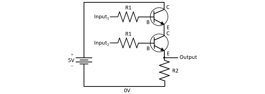
Figure 2.5: Transistor AND gate
Table 2.2 is the truth table for the AND gate circuit. In simple terms, the Output signal is true (at the 1 level) when both the Input1 and Input2 inputs are true, and false (0) otherwise.
Table 2.2: AND gate truth table

The AND gate has its own schematic symbol, shown in Figure 2.6:

Figure 2.6: AND gate schematic symbol
An OR gate has an output of 1 when either the A or B input is 1, and also if both inputs are 1. Here is the truth table for the OR gate.
Table 2.3: OR gate truth table

The OR gate schematic symbol is shown in Figure 2.7:

Figure 2.7: OR gate schematic symbol
The exclusive-OR, or XOR, operation produces an output of 1 when just one of the A and B inputs is 1. The output is 0 when both inputs are 0 and when both are 1. Here is the XOR truth table.
Table 2.4: XOR gate truth table

The XOR gate schematic symbol is shown in Figure 2.8:

Figure 2.8: XOR gate schematic symbol
Each of the AND, OR, and XOR gates can be implemented with an inverting output. The function of the gate is exactly the same as described in the preceding section, except the output is inverted (0 is replaced with 1 in the Output column in Table 2.2, Table 2.3, and Table 2.4, and 1 is replaced with 0). The schematic symbol for an AND, OR, or XOR gate with inverted output has a small circle added on the output side of the symbol, just as on the output of the NOT gate. The names of the gates with inverted outputs are NAND, NOR, and XNOR. The letter 'N' in each of these names indicates NOT. For example, NAND means NOT AND, which is functionally equivalent to an AND gate followed by a NOT gate.
Low-level logic gates can be combined to produce more complex functions. A multiplexer is a circuit that selects one of multiple inputs to pass through to an output based on the state of a selector input. Figure 2.9 is a diagram of a two-input multiplexer:
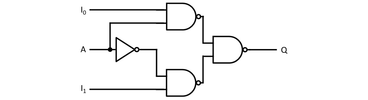
Figure 2.9: Two-input multiplexer circuit
The two single-bit data inputs are I0 and I1. The selector input A passes the value of I0 through to the output Q when A is high. It passes I1 to the output when A is low. One use of a multiplexer in processor design is to select input data from one of multiple sources when loading an internal register.
The truth table representation of the two-input multiplexer is shown in. In this table, the value X indicates "don't care", meaning it does not matter what value that signal has in determining the Q output.
Table 2.5: Two-input multiplexer truth table

The logic gates presented in this section, and the circuits made by combining them, are referred to as combinational logic when the output at any moment depends only on the current state of the inputs. For the moment, we're ignoring propagation delay and assuming that the output responds immediately to changes in the inputs. In other words, the output does not depend on prior input values. Combinational logic circuits have no memory of past inputs or outputs.
Latches
Combinational logic does not directly permit the storage of data as is needed for digital functions such as processor registers. Logic gates can be used to create data storage elements through the use of feedback from a gate output to an input.
The latch is a single-bit memory device constructed from logic gates. Figure 2.10 shows a simple type of latch called the Set-Reset, or SR, latch. The feature that provides memory in this circuit is the feedback from the output of the AND gate to the input of the OR gate:

Figure 2.10: SR latch circuit
Based on the inputs S and R, the circuit can either set the output Q to high, reset Q to low, or cause the output Q to be held at its last value. In the hold state, both S and R are low, and the state of the output Q is retained. Pulsing S high (going from low to high then back to low) causes the output Q to go high and remain at that level. Pulsing R high causes Q to go low and stay low. If both S and R are set high, the R input overrides the S input and forces Q low.
The truth table for the SR latch is shown in Table 2.6. The output Qprev represents the most recent value of Q selected through the actions of the S and R inputs.
Table 2.6: SR latch truth table

One item to be aware of with this latch circuit, and with volatile memory devices in general, is that the initial state of the Q output upon power-up is not well defined. The circuit startup behavior and the resulting value of Q depend on the characteristics and timing of the individual gates as they come to life. After power-on, and prior to beginning use of this circuit for productive purposes, it is necessary to pulse the S or R input to place Q into a known state.
The gated D latch, where D stands for data, has many uses in digital circuits. The term gated refers to the use of an additional input that enables or inhibits the passage of data through the circuit. Figure 2.11 shows an implementation of the gated D latch:

Figure 2.11: Gated D latch circuit
The D input passes through to the Q output whenever the E (Enable) input is high. When E is low, the Q output retains its previous value regardless of the state of the D input. The Q output always holds the inverse of the Q output (the horizontal bar on Q means NOT).
Table 2.7: Gated D latch truth table

It is worth taking a moment to trace the logical flow of this circuit to understand its operation. The left half of Figure 2.11, consisting of the D input, the NOT gate, and the two leftmost NAND gates, is a combinational logic circuit, meaning the output is always a direct function of the input.
First, consider the case when the E input is low. With E low, one of the inputs to each of the two left-hand NAND gates is low, which forces the output of both gates to 1 (refer to Table 2.2 and the AND gate truth table, and remember that the NAND gate is equivalent to an AND gate followed by a NOT gate). In this state, the value of the D input is irrelevant, and one of Q or Q must be high and the other must be low, because of the cross-connection of the outputs of the two rightmost NAND gates feeding back to the gate inputs. This state will be retained as long as E is low.
When E is high, depending on the state of D, one of the two leftmost NAND gates will have a low output and the other will have a high output. The one with the low output will drive the connected rightmost NAND gate to a high output. This output will feed back to the input of the other right-hand side NAND gate and, with both inputs high, will produce a low output. The result is that the input D will propagate through to the output Q and the inverse of D will appear at output Q.
It is important to understand that Q and Q cannot both be high or low at the same time, because this would represent a conflict between the outputs and inputs of the two rightmost NAND gates. If one of these conditions happens to arise fleetingly, such as during power-up, the circuit will self-adjust to a stable configuration, with Q and Q holding opposite states. As with the SR latch, the result of this self-adjustment is not predictable, so it is important to initialize the gated D latch to a known state before using it in any operations. Initialization is performed by setting E high, setting D to the desired initial Q output, and then setting E low.
The gated D latch described previously is a level-sensitive device, meaning that the output Q changes to follow the D input as long as the E input is held high. In more complex digital circuits, it becomes important to synchronize multiple circuit elements connected in series without the need to carefully account for propagation delays across the individual devices. The use of a shared clock signal as an input to multiple elements enables this type of synchronization. In a shared-clock configuration, components update their outputs based on clock signal edges (edges are the moments of transition from low to high or high to low) rather than directly based on high or low input signal levels.
Edge triggering is useful because the clock signal edges identify precise moments at which device inputs must be stable. After the clock edge has passed, the device's inputs are free to vary in preparation for the next active clock edge without the possibility of altering the outputs. The flip-flop circuit, discussed next, responds to clock edges, providing this desirable characteristic for use in complex digital designs.
Flip-flops
A device that changes its output state only when a clock signal makes a specified transition (either low-to-high or high-to-low) is referred to as an edge-sensitive device. Flip-flops are similar to latches, with the key difference being that the output of a flip-flop changes in response to a signal edge rather than responding to the signal level.
The positive edge-triggered D flip-flop is a popular digital circuit component used in a variety of applications. The D flip-flop typically includes set and reset input signals that perform the same functions as in the SR latch. This flip-flop has a D input that functions just like the D input of the gated D latch. Instead of an enable input, the D flip-flop has a clock input that triggers the transfer of the D input to the Q output and, with inversion, to the Q output on the clock's rising edge. Other than within a very narrow time window surrounding the rising edge of the clock signal, the flip-flop does not respond to the value of the D input. When active, the S and R inputs override any activity on the D and clock inputs.
Figure 2.12 shows the schematic symbol for the D flip-flop. The clock input is indicated by the small triangle on the left-hand side of the symbol:

Figure 2.12: D flip-flop schematic symbol
Consider the following table. The upward-pointing arrows in the CLK column indicate the rising edge of the clock signal. The Q and outputs shown in the table rows with upward-pointing arrows represent the state of the outputs following the rising clock edge.
Table 2.8: D flip-flop truth table

Flip-flops can be connected in series to enable the transfer of data bits from one flip-flop to the next. This is achieved by connecting the Q output of the first flip-flop to the D input of the second one, and so on for any number of stages. This structure is called a shift register and has many applications, two of which are serial-to-parallel conversion and parallel-to-serial conversion.
If the Q output at the end of a shift register is connected to the D input at the other end, the result is a ring counter. Ring counters are used for tasks such as the construction of finite state machines. Finite state machines implement a mathematical model that is always in one of a set of well-defined states. Transitions between states occur when inputs satisfy the requirements to transition to a different state.
The ring counter in Figure 2.13 has four positions. The counter is initialized by pulsing the RST input high and then low. This sets the Q output of the first (leftmost) flip-flop to 1 and the remaining flip-flop Q outputs to 0. After that, each rising edge of the CLK input transfers the 1 bit to the next flip-flop in the sequence. The fourth CLK pulse transfers the 1 back to the leftmost flip-flop. At all times, all of the flip-flops have a Q output of 0 except for one that has a 1 output. The flip-flops are edge-sensitive devices and all of them are driven by a common clock signal, making this a synchronous circuit:

Figure 2.13: Four-position ring counter circuit
This circuit contains four ring counter states. Adding six more flip-flops would bring the number of states to 10. As we discussed in Chapter 1, Introducting Computer Architecture, the ENIAC used vacuum tube-based 10-position ring counters to maintain the state of decimal digits. A 10-state ring counter based on the circuit in Figure 2.13 can perform the same function.
In the next section, we will construct registers for data storage from flip-flops.
Registers
Processor registers temporarily store data values and serve as input to and output from a variety of instruction operations, including data movement to and from memory, arithmetic, and bit manipulation. Most general-purpose processors include instructions for shifting binary values stored in registers to the left or right, and for performing rotation operations in which data bits shifted out one end of the register are inserted at the opposite end. The rotation operation is similar to the ring counter, except that the bits in a rotation can hold arbitrary values, while a ring counter typically transfers a single 1 bit through the sequence of locations. Circuits performing these functions are constructed from the low-level gates and flip-flops discussed earlier in this chapter.
Registers within a processor are usually loaded with data values and read out in parallel, meaning all the bits are written or read on separate signal lines simultaneously under the control of a common clock edge. The examples presented in this section will use four-bit registers for simplicity, but it is straightforward to extend these designs to 8, 16, 32, or 64 bits as needed.
Figure 2.14 shows a simple four-bit register with parallel input and output. This is a synchronous circuit, in which data bits provided on inputs D0-D3 are loaded into the flip-flops on the rising edge of the CLK signal. The data bits appear immediately at the Q0-Q3 outputs and retain their state until new data values are loaded on a subsequent rising clock edge:

Figure 2.14: Four-bit register circuit
To perform useful functions beyond simply storing data in the register, it is necessary to be able to load data from multiple sources into the register, perform operations on the register contents, and write the resulting data value to one of potentially many destinations.
In general-purpose processors, a data value can usually be loaded into a register from a memory location or an input port, or transferred from another register. Operations performed on the register contents might include incrementing, decrementing, arithmetic, shifting, rotating, and bit operations such as AND, OR, and XOR. Note that incrementing or decrementing an integer is equivalent to addition or subtraction of an operand with a second implied operand of 1. Once a register contains the result of a computation, its contents can be written to a memory location, to an output port, or to another register.
Figure 2.9 presented a circuit for a two-input multiplexer. It is straightforward to extend this circuit to support a larger number of inputs, any of which can be selected by control inputs. The single-bit multiplexer can be replicated to support parallel operation across all the bits in a processor word. Such a circuit can be used to select among a variety of sources when loading a register with data. When implemented in a processor, logic triggered by instruction opcodes sets the multiplexer control inputs to route data from the appropriate source to the specified destination register. Chapter 3, Processor Elements, will expand on the use of multiplexers for data routing to registers and to other units within the processor.
The next section will introduce circuits that add binary numbers.
Adders
General-purpose processors usually support the addition operation for performing calculations on data values and, separately, to manage the instruction pointer. Following the execution of each instruction, the instruction pointer increments to the next instruction location. When the processor supports multi-word instructions, the updated instruction pointer must be set to its current value plus the number of words in the just-completed instruction.
A simple adder circuit adds two data bits plus an incoming carry and produces a one-bit sum and a carry output. This circuit, shown in Figure 2.15, is called a full adder because it includes the incoming carry in the calculation. A half adder adds only the two data bits without an incoming carry:

Figure 2.15: Full adder circuit
The full adder uses logic gates to produce its output as follows. The sum bit S is 1 only if the total number of 1 bits in the group A, B, Cin is an odd number. Otherwise, S is 0. The two XOR gates perform this logical operation. Cout is 1 if both A and B are 1, or if just one of A and B is 1 and Cin is also 1. Otherwise, Cout is 0.
The circuit in Figure 2.15 can be condensed to a schematic block with three inputs and two outputs for use in higher-level diagrams. Figure 2.16 is a four-bit adder with four blocks representing copies of the full adder circuit of Figure 2.15. The inputs are the two words to be added, A0-A3 and B0-B3, and the incoming carry, Cin. The output is the sum, S0-S3, and the outgoing carry, Cout:

Figure 2.16: 4-bit adder circuit
It is important to note that this circuit is a combinational circuit, meaning that once the inputs have been set, the outputs will be generated directly. This includes the carry action from bit to bit, no matter how many bits are affected by carries. Because the carry flows across bit by bit, this configuration is referred to as a ripple carry adder. It takes some time for the carries to propagate across all the bit positions and for the outputs to stabilize at their final value.
Since we are now discussing a circuit with a signal path that passes through a significant number of devices, it is appropriate to discuss the implications of the time required for signals to travel from end to end across multiple components.
Propagation delay
When the input of a logic device changes, the output does not change instantly. There is a time delay between a change of state at the input and the final result appearing at the output called the propagation delay.
Placing multiple combinational circuits in series results in an overall propagation delay that is the sum of the delays of all the intermediate devices. A gate may have a different propagation delay for a low-to-high transition than for a high-to-low transition, so the larger of these two values should be used in the estimation of the worst-case delay.
From Figure 2.15, the longest path (in terms of the number of gates in series) from input to output for the full adder is from the A and B inputs to the Cout output: a total of three sequential gates. If all of the input signals in Figure 2.16 are set simultaneously on the full adder inputs, the three-gate delay related to those inputs will take place simultaneously across all the adders. However, the C0 output from Full Adder 0 is only guaranteed to be stable after the three-gate delay across Full Adder 0. Once C0 is stable, there is an additional two-gate delay across Full Adder 1 (note that in Figure 2.15, Cin only passes through two sequential levels of gates).
The overall propagation delay for the circuit in Figure 2.16 is therefore three gate delays across Full Adder 0 followed by two gate delays across each of the remaining three full adders, a total of nine gate delays. This may not seem too bad, but consider a 32-bit adder: the propagation delay for this adder is three gate delays for Full Adder 0 plus two gate delays for each of the remaining 31 adders, a total of 65 gate delays.
The path with the maximum propagation delay through a combinational circuit is called the critical path, and this delay places an upper limit on the clock frequency that can be used to drive the circuit.
Logic gates from the Advanced Schottky Transistor-Transistor Logic family, abbreviated (AS) TTL, are among the fastest individually packaged gates available today. An (AS) TTL NAND gate has a propagation delay of 2 nanoseconds (ns) under typical load conditions. For comparison, light in a vacuum travels just under two feet in 2 ns.
In the 32-bit ripple carry adder, 65 propagation delays through (AS) TTL gates result in a delay of 130 ns between setting the inputs and receiving final, stable outputs. For the purpose of forming a rough estimate, let's assume this is the worst-case propagation delay through an entire processor integrated circuit. We'll also ignore any additional time required to hold inputs stable before and after an active clock edge. This adder, then, cannot perform sequential operations on input data more often than once every 130 ns.
When performing 32-bit addition with a ripple carry adder, the processor uses a clock edge to transfer the contents of two registers (each consisting of a set of D flip-flops) plus the processor C flag to the adder inputs. The subsequent clock edge loads the results of the addition into a destination register. The C flag receives the value of Cout from the adder.
A clock with a period of 130 ns has a frequency of (1/130 ns), which is 7.6 MHz. This certainly does not seem very fast, especially when many low-cost processors are available today with clock speeds in excess of 4 GHz. Part of the reason for this discrepancy is the inherent speed advantage of integrated circuits containing massive numbers of tightly packed transistors, and the other part is the result of the cleverness of designers, as referenced by Gordon Moore in Chapter 1, Introducting Computer Architecture. To perform the adder function efficiently, many design optimizations have been developed to substantially reduce the worst-case propagation delay. Chapter 8, Performance-Enhancing Techniques, will discuss some of the methods processor architects use to wring higher speeds from their designs.
In addition to gate delays, there is also some delay resulting from signal travel through wires and integrated circuit conductive paths. The propagation speed through a conductive path varies depending on the material used for conduction and the insulating material surrounding the conductor. Depending on these and other factors, the propagation speed in digital circuits is typically 50-90% of the speed of light in a vacuum.
The next section discusses the generation and use of clocking signals in digital circuits.
Clocking
The clock signal serving as the heartbeat of a processor is usually a square wave signal operating at a fixed frequency. A square wave is a digital signal that oscillates between high and low states, spending equal lengths of time at the high and low levels on each cycle. Figure 2.17 shows an example of a square wave over time:

Figure 2.17: Square wave signal
The clock signal in a computer system is usually generated with a crystal oscillator providing a base frequency of a few megahertz (MHz). 1 MHz is 1 million cycles per second. A crystal oscillator relies on the resonant vibration of a physical crystal, usually made of quartz, to generate a cyclic electrical signal using the piezoelectric effect. Quartz crystals resonate at precise frequencies, which leads to their use as timing elements in computers, wristwatches, and other digital devices.
Although crystal oscillators are more accurate time references than alternative timing references that may be used in low-cost devices, crystals exhibit errors in frequency that accumulate over periods of days and weeks to gradually drift by seconds and then minutes away from the correct time. To avoid this problem, most Internet-connected computers access a time server periodically to reset their internal clocks to the current time as defined by a precise atomic reference clock.
Phase-locked loop (PLL) frequency multiplier circuits are used to generate the high-frequency clock signals needed by multi-GHz processors. A PLL frequency multiplier generates a square wave output frequency at an integer multiple of the input frequency provided to it from the crystal oscillator. The ratio of the PLL clock output frequency to the input frequency it receives is called the clock multiplier.
A PLL frequency multiplier operates by continuously adjusting the frequency of its internal oscillator to maintain the correct clock multiplier ratio relative to the PLL input frequency. Modern processors usually have a crystal oscillator clock signal input and contain several PLL frequency multipliers producing different frequencies. Different clock multiplier values are used to drive core processor operations at the highest possible speed while simultaneously interacting with devices that require lower clock frequencies, such as system memory.
Sequential logic
Digital circuitry that generates outputs based on a combination of current inputs and past inputs is called sequential logic. This is in contrast to combinational logic, in which outputs depend only on the current state of the inputs. When a sequential logic circuit composed of several components operates those components under the control of a shared clock signal, the circuit implements synchronous logic.
The steps involved in the execution of processor instructions take place as a series of discrete operations that consume input in the form of instruction opcodes and data values received from various sources. This activity takes place under the coordination of a master clock signal. The processor maintains internal state information from one clock step to the next, and from one instruction to the next.
Modern complex digital devices, including processors, are almost always implemented as synchronous sequential logic devices. Low-level internal components, such as the gates, multiplexers, registers, and adders discussed previously, are usually combinational logic circuits. These lower-level components, in turn, are provided inputs under the control of synchronous logic. After allowing sufficient time for propagation across the combinational components, the shared clock signal transfers the outputs of those components into other portions of the architecture under the control of processor instructions and the logic circuits that carry out those instructions.
Chapter 3, Processor Elements, will introduce the higher-level processor components that implement more complex functionality, including instruction decoding, instruction execution, and arithmetic operations.
The next section introduces the concept of designing digital hardware using computer programming languages.
Hardware description languages
It is straightforward to represent simple digital circuits using logic diagrams similar to the ones presented earlier in this chapter. When designing digital devices that are substantially more complex, however, the use of logic diagrams quickly becomes unwieldy. As an alternative to the logic diagram, a number of hardware description languages have been developed over the years. This evolution has been encouraged by Moore's Law, which drives digital system designers to continually find new ways to quickly make the most effective use of the constantly growing number of transistors available in integrated circuits.
Hardware description languages are not the exclusive province of digital designers at semiconductor companies; even hobbyists can acquire and use these powerful tools at an affordable cost, even for free in many cases.
A gate array is a logic device containing a large number of logic elements such as NAND gates and D flip-flops that can be connected to form arbitrary circuits. A category of gate arrays called field programmable gate arrays (FPGAs) enables end users to implement their own designs into gate array chips using just a computer, a small development board, and an appropriate software package.
A developer can define a complex digital circuit using a hardware description language and program it into a chip directly, resulting in a fully functional, high-performance custom digital device. Current-generation low-cost FPGAs contain a sufficient number of gates to implement complex modern processor designs. As one example, an FPGA-programmable design of the RISC-V processor (discussed in detail in Chapter 11, The RISC-V Architecture and Instruction Set) is available in the form of open source hardware description language code.
VHDL
VHDL is one of the leading hardware description languages in use today. Development of the VHDL language began in 1983 under the guidance of the U.S. Department of Defense. The syntax and some of the semantics of VHDL are based on the Ada programming language, which, incidentally, is named after Ada Lovelace, the programmer of Charles Babbage's Analytical Engine, discussed in Chapter 1, Introducting Computer Architecture. Verilog is another popular hardware design language with capabilities similar to VHDL. This book will use VHDL exclusively, but the examples could be implemented just as easily in Verilog.
VHDL is a multilevel acronym where the V stands for VHSIC, which means Very High-Speed Integrated Circuit, and VHDL stands for VHSIC Hardware Description Language. The following code presents a VHDL implementation of the full adder circuit shown in Figure 2.15:
-- Load the standard libraries
library IEEE;
use IEEE.STD_LOGIC_1164.ALL;
-- Define the full adder inputs and outputs
entity FULL_ADDER is
port (
A : in std_logic;
B : in std_logic;
C_IN : in std_logic;
S : out std_logic;
C_OUT : out std_logic
);
end entity FULL_ADDER;
-- Define the behavior of the full adder
architecture BEHAVIORAL of FULL_ADDER is
begin
S <= (A XOR B) XOR C_IN;
C_OUT <= (A AND B) OR ((A XOR B) AND C_IN);
end architecture BEHAVIORAL;
This code is a fairly straightforward textual description of the full adder in Figure 2.15. Here, the section introduced with entity FULL_ADDER is defines the inputs and outputs of the full adder component. The architecture section toward the end of the code describes how the circuit logic operates to produce the outputs S and C_OUT given the inputs A, B, and C_IN. The term std_logic refers to a single-bit binary data type. The <= characters represent wire-like connections, driving the output on the left-hand side with the value computed on the right-hand side.
The following code references the FULL_ADDER VHDL as a component in the implementation of the four-bit adder design presented in Figure 2.16:
-- Load the standard libraries
library IEEE;
use IEEE.STD_LOGIC_1164.ALL;
-- Define the 4-bit adder inputs and outputs
entity ADDER4 is
port (
A4 : in std_logic_vector(3 downto 0);
B4 : in std_logic_vector(3 downto 0);
SUM4 : out std_logic_vector(3 downto 0);
C_OUT4 : out std_logic
);
end entity ADDER4;
-- Define the behavior of the 4-bit adder
architecture BEHAVIORAL of ADDER4 is
-- Reference the previous definition of the full adder
component FULL_ADDER is
port (
A : in std_logic;
B : in std_logic;
C_IN : in std_logic;
S : out std_logic;
C_OUT : out std_logic
);
end component;
-- Define the signals used internally in the 4-bit adder
signal c0, c1, c2 : std_logic;
begin
-- The carry input to the first adder is set to 0
FULL_ADDER0 : FULL_ADDER
port map (
A => A4(0),
B => B4(0),
C_IN => '0',
S => SUM4(0),
C_OUT => c0
);
FULL_ADDER1 : FULL_ADDER
port map (
A => A4(1),
B => B4(1),
C_IN => c0,
S => SUM4(1),
C_OUT => c1
);
FULL_ADDER2 : FULL_ADDER
port map (
A => A4(2),
B => B4(2),
C_IN => c1,
S => SUM4(2),
C_OUT => c2
);
FULL_ADDER3 : FULL_ADDER
port map (
A => A4(3),
B => B4(3),
C_IN => c2,
S => SUM4(3),
C_OUT => C_OUT4
);
end architecture BEHAVIORAL;
This code is a textual description of the four-bit adder in Figure 2.16. Here, the section introduced with entity ADDER4 is defines the inputs and outputs of the four-bit adder component. The phrase std_logic_vector(3 downto 0) represents a four-bit data type with bit number 3 in the left-hand (most significant) position and bit number 0 on the right-hand side.
The FULL_ADDER component is defined in a separate file, referenced here by the section beginning component FULL_ADDER is. The statement signal c0, c1, c2 : std_logic; defines the internal carry values between the full adders. The four port map sections define the connections between the four-bit adder signals and the inputs and outputs of each of the single-bit full adders. To reference a bit in a multi-bit value, the bit number follows the parameter name in parentheses. For example, A4(0) refers to the least significant of the four bits in A4.
Note the use of hierarchy in this design. A simple component, the single-bit full adder, was first defined as a discrete, self-contained block of code. This block was then used to construct a more complex circuit, the four-bit adder. This hierarchical approach can be extended through many levels to define an extremely complex digital device constructed from less complex components, each of which, in turn, is constructed from even simpler parts. This general approach is used routinely in the development of modern processors containing hundreds of millions of transistors, while managing complexity in a manner that keeps the design understandable by humans at each level of the architectural hierarchy.
The code in this section provides all the circuit information that a logic synthesis software tool suite requires to implement the four-bit adder as a component in an FPGA device. Of course, additional circuitry is required to present meaningful inputs to the adder circuit and then to process the results of an addition operation after allowing for propagation delay.
This has been a very brief introduction to VHDL. The intent here has been to make you aware that hardware description languages such as VHDL are the current state of the art in complex digital circuit design. In addition, you should know that some very low-cost options are available for FPGA development tools and devices. The exercises at the end of this chapter will introduce you to some highly capable FPGA development tools at no cost. You are encouraged to search the Internet and learn more about VHDL and other hardware description languages and try your hand at developing some simple (and not-so-simple) circuit designs.
Summary
This chapter began with an introduction to the properties of electrical circuits and showed how components such as voltage sources, resistors, and wires are represented in circuit diagrams. The transistor was introduced, with a focus on its use as a switching element in digital circuits. The NOT gate and the AND gate were constructed from transistors and resistors. Additional types of logic gates were defined and truth tables were presented for each one. Logic gates were used to construct more complex digital circuits, including latches, flip-flops, registers, and adders. The concept of sequential logic was introduced, and its applicability to processor design was discussed. Finally, hardware description languages were introduced, and a four-bit adder example was presented in VHDL.
You should now have an understanding of the basic digital circuit concepts and design tools used in the development of modern processors. The next chapter will expand upon these building blocks to explore the functional components of modern processors, leading to a discussion of how those components coordinate to implement the primary processor operational cycle of instruction loading, decoding, and execution.
Exercises
- Rearrange the circuit in Figure 2.5 to convert the AND gate to a NAND gate. Hint: there is no need to add or remove components.
- Create a circuit implementation of an OR gate by modifying the circuit in Figure 2.5. Wires, transistors, and resistors can be added as needed.
- Search the Internet for free VHDL development software suites that include a simulator. Get one of these suites, set it up, and build any simple demo projects that come with the suite to ensure it is working properly.
- Using your VHDL tool set, implement the four-bit adder using the code listings presented in this chapter.
- Add test driver code (search the Internet to learn how) to your four-bit adder to drive it through a limited set of input sets and verify that the outputs are correct.
- Expand the test driver code and verify that the four-bit adder produces correct results for all possible combinations of inputs.