3
STM32CubeMX Application
In this chapter I present an in-depth discussion of the STM32CubeMX application, which is a free utility provided by STMicroelectronics (STM). I will also start referring to it as CubeMX to just simplify the terminology. I would also like to acknowledge a fine Leanpub eBook published by Carmine Noviello titled Mastering STM32. Carmine’s book was invaluable reference alongside the STM datasheets without which I could not have created this book.
CubeMX is a fairly complex utility because it is intended to encompass nearly all the microcontroller chips (MCUs) and development boards that STM offers. This is quite an amazing feat considering that there are hundreds of MCU variants and dozens of development boards that STM manufactures. The CubeMX supports these devices by automatically generating C code that developers can easily use in their programs. The generated code is designed to support specific integrated peripheral (IP) devices included on the selected MCU. CubeMX may be regarded as a MCU-centric utility because of the following features:
• MCU selection based on the STM family, that is, F0, F1, …
• Specific IP required for the project involving mapping MCU peripherals to a specific pinout
• Handles specific MCU clock, power, interrupt control, ...
• Automatically adapts pinout to package configuration
• Manages the ST hardware abstraction layer (ST HAL)
• Manages external libraries
• Adaptable to a variety of IDEs
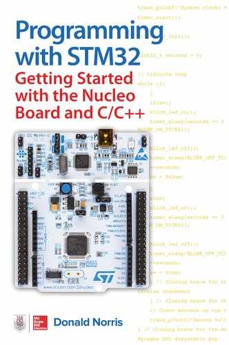
Figure 3-1 shows the opening screen when the application is initially launched.
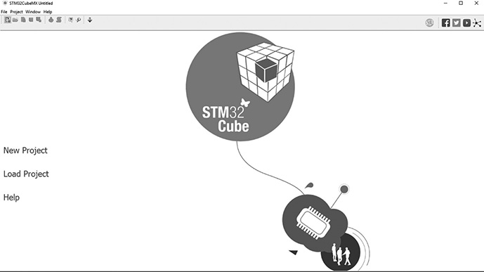
Figure 3-1 CubeMX opening screen.
There are three choices available on the screen:
• New Project
• Load Project
• Help
The New Project selection will be shortly discussed in-depth, but I do first want to briefly mention what happens with the other two selections. Clicking on Load Project will display the open file dialog box, as shown in Figure 3-2.
Figure 3-2 Load Project screen shot.
In this figure there is only one project file named Hello.ioc, which is located in a project directory that is automatically created whenever a new project is created. The project directory is named using the same name entered in the new project dialog box. The project file contains everything that CubeMX needs to reconstitute the project in order to continue with any development efforts.
Clicking on the Help selection will display the opening page of a PDF document, as shown in Figure 3-3.
Figure 3-3 Opening page for CubeMX Help document.
This PDF revision is a 261-page document that carefully details all the many features and functions contained within the CubeMX application. I would strongly recommend that you select and open this document and then save it to any convenient directory. In that way, you will always have access to the help document without needing to open the CubeMX application itself. You should also consider printing applicable portions of the document to have ready reference to appropriate material while using the application.
Clicking on the New Project selection will display a page with two tab selections. One tab is entitled MCU Selector and the other is Board Selector. Clicking on the Board Selector will cause the dialog box shown in Figure 3-4 to appear.
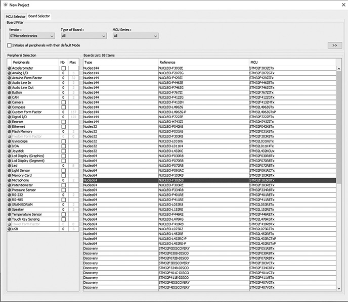
Figure 3-4 Board Selector dialog screen shot.
I selected a Nucleo64 as the board type and NUCLEO-F302R8 as the reference as may be seen in the figure, which matched the demonstration board I selected to use in this book. Figure 3-5 shows the result of selecting this particular board.
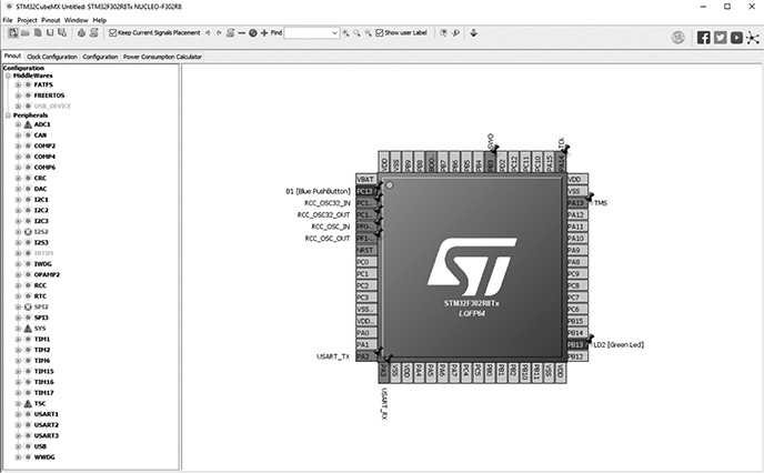
Figure 3-5 NUCLEO-F302R8 board selection.
There are four tabs shown in this figure, which I will discuss here one by one. These tabs, displayed from left to right, are as follows:
• Pinout
• Clock Configuration
• Configuration
• Power Consumption Calculator
Pinout Tab
Figure 3-5 shows the Pinout tab display, which is divided into two parts. The right-hand side shows the selected board MCU with all predesignated peripheral and GPIO pins clearly shown. ST refers to this as the Chip view for obvious reasons. These pin designations will be explored in detail in later sections as well as later chapters. The left-hand portion of the Pinout display in Figure 3-5 shows all the peripheral pins as well as software MiddleWares in a tree view. Next to each tree element is a symbol, which reflects the individual status of the peripheral or software line item. I will discuss these symbols after discussing Chip view and exploring the significant amount of information that can be gained from this view.
Figure 3-6 is an expanded diagram of the STM32F302R8Tx MCU chip that is used as the core processor in the NUCLEO-F411RE development board.
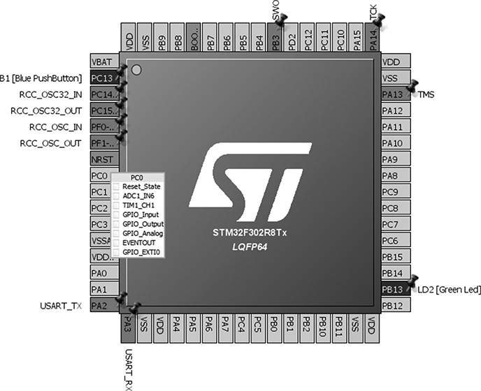
Figure 3-6 STM32F302R8Tx MCU.
NOTE It will be somewhat difficult for readers of the hard copy book to follow the next discussion as the figure uses color coded pins, which are very hard to distinguish in the gray-scaled rendered images. Therefore, I will attempt to identify the pins under discussion as completely as I can, given this constraint.
There are two fully enabled GPIO pins colored in green, which are PC13 and PB13. PC13 is located near the top left-hand corner, while PB13 is at the lower right-hand corner. Pin PC13 is permanently connected to the development board’s user blue push button and PB13 is permanently connected to the user green LED. These connections are also noted in the diagram, as shown in Figure 3-6.
There are nine orange-coded pins located on all four sides of the board. An orange-coded pin indicates that a peripheral normally assigned to a specific pin has not been enabled. For example, PA2 and PA3 are located on either side of the lower left-hand corner of Figure 3-6 and have the peripheral USART TX and RX functions assigned to each pin, respectively. Being orange coded will mean that the CubeMX application will not automatically generate any C code that will enable the USART functions for these pins.
All of the yellow-coded pins are typically located at or near the corners of the chip and are solely dedicated to power source functions with designations such as Vdd, Vss, Vbat, and Vca. These pins are strict hardware designations and cannot be programmed or reconfigured.
Finally, there are two remaining olive colored pins, BOOT and NRST, with BOOT located on the top edge and NRST located on the left edge. Like the power source pins, these two pins have dedicated MCU functions and cannot be programmed or reconfigured.
All remaining pins in the Chip view are gray-coded GPIO pins and can be initialized to suit program requirements. How this is accomplished is thoroughly discussed in the next chapter. All these pins have various functions or status outputs, which may be revealed by hovering the mouse over a particular pin. The functions and status outputs for pin PC0 as shown in Figure 3-6 are as follows:
• Reset_State
• ADC1_IN6
• TIM1_CH1
• GPIO_Input
• GPIO_Output
• GPIO_Analog
• EVENTOUT
• GPIO_EXTI0
It would be difficult at this point to explain each of these functions and status outputs. They are all discussed in the comprehensive STM32F302R8 MCU datasheet. The GPIO functions, however, will be discussed in the next chapter.
MCU Alternative Functions
The STM MCU architecture allows for alternative pin mapping for various peripheral functions. Control clicking on any enabled GPIO pin such as PC13 will reveal the alternate pin mappings associated with that pin, as shown in Figure 3-7.
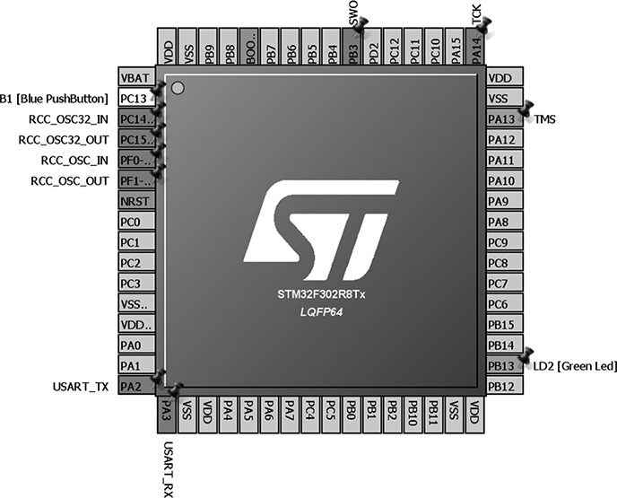
Figure 3-7 PC13 alternative pin mappings.
All available alternative pins will immediately be color-coded blue in response to control clicking on a selected pin. In Figure 3-7, the alternative pins are PA13 and PB13, but only if the alternative pin(s) are not in a reset state. Using alternative mapping allows for optimized board layout if it is inconvenient to layout a trace to the primary pin. The CubeMX will attempt to automatically resolve pin layout conflicts whenever detected by assigning a peripheral function to an alternative pin. However, by placing a logical “push pin” on a selected MCU pin will lock a desired peripheral function to a pin. These “push pins” are easily seen in the figure. These pins prevent CubeMX from enabling an alternative mapping of the locked pins. Pins locked out from alternative mapping are also color coded orange.
Integrated Peripheral (IP) Tree Pane
The IP tree pane shown in the left-hand side of Figure 3-6 allows a CubeMX user an easy way to enable or disable peripherals that may be assigned to a MCU pin. The tree pane also allows the user to enable certain software middleware libraries. The tree listing uses a variety of colored icons and text to indicate the peripheral status and configuration. Figure 3-8 shows these colored icons and textual meanings associated with each of them. This figure is excerpted from the CubeMX user manual, which I urge interested readers to download and save. There is a wealth of information available in the 261-page PDF manual, which I simply do not have the space to cover.
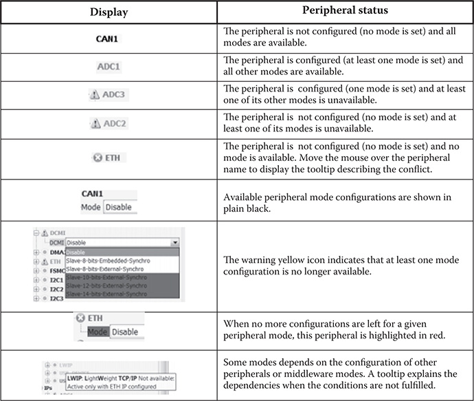
Figure 3-8 Tree pane IP icons and textual descriptions.
Clock Configuration Tab
The STM32 series of MCUs use a very flexible approach to configure a variety of clock sources needed for MCU operations. These sources apply to both core MCU functions and most of the peripheral functions. Clock sources and the associated phase-locked loops (PLL) are shown graphically in Figure 3-9, which will be displayed when you click on the Clock Configuration tab.
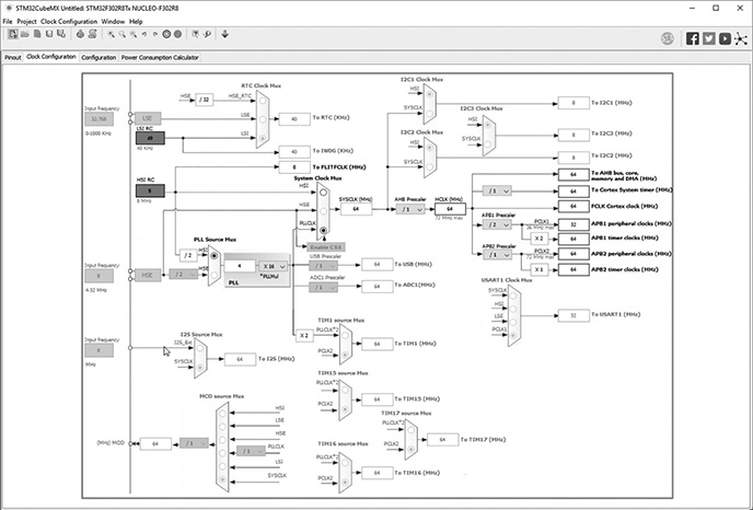
Figure 3-9 Clock Configuration GUI.
Figure 3-9 appears a bit daunting at first glance, but do not despair as it is really not that complicated, especially after you interact with it a few times. The STM32 clock sourcing is very much capable and flexible as compared to ordinary 8-bit MCUs.
The very first thing that must be considered is the basic clock sources. There is a high-speed clock (HSE) and a low-speed clock (LSE) used for the STM32 MCU series. These clocks may be sourced either internally or externally. These clocks will be internally sourced for all of this book’s projects; however, either one or both can be externally sourced if so desired. You must first enable the appropriate clock input pins if it desired to use external clock(s). This is done by returning to the IP tree in the Pinout view and expand the RCC section. Figure 3-10 shows a typical configuration for these pins.
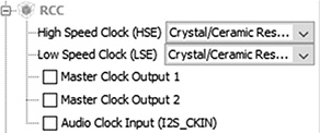
Figure 3-10 RCC pin configurations.
You must return to the Clock Configuration tab once the clock input pins have been enabled and complete the clock source configurations.
There will be no need to change any of the clock configurations because they are perfectly suitable to support all book projects as they are set in their default states. I do want to caution readers who might be considering overclocking the MCU. Overclocking is a common hack that users will sometimes attempt in order to “gain” some perceived performance increase from a computer system. Overclocking is especially prevalent in gaming systems where high clock rates are thought to improve display frame rates and game performance. While this may be true for some gaming systems, the undue stress due to much higher chip heat dissipation will shorten processor life considerably. Gaming systems also employ sophisticated cooling subsystems, which are not present in the STM Nucleo board series. The bottom line is to NOT overclock as that will definitely overheat the MCU and cause it to prematurely fail.
Configuration View Tab
The Configuration View provides an overview for all of the software configurable components including GPIOs, peripherals, and middleware. There are clickable buttons, as can be seen in Figure 3-11, which allow for configuration options for various components. The CubeMX application will automatically create the supporting C/C++ code that supports the desired configuration.
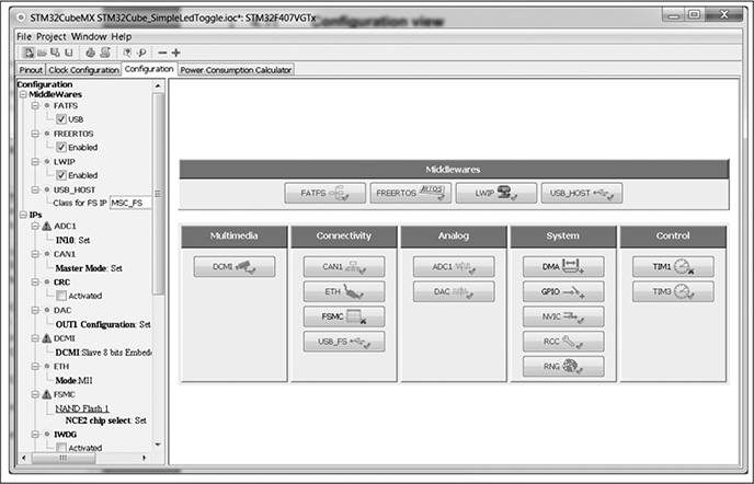
Figure 3-11 Configuration View.
There are color-coded icons and text in Figure 3-11, in much similar fashion to what was displayed in the IP tree pane view. Figure 3-12 details what the icons and text mean as they are applied to the Configuration View.
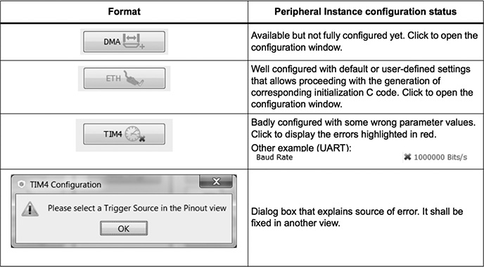
Figure 3-12 Configuration View icons and textual descriptions.
Power Consumption Calculator View Tab
Clicking on the remaining tab will display an uninitialized power consumption calculator screen, as shown in Figure 3-13.
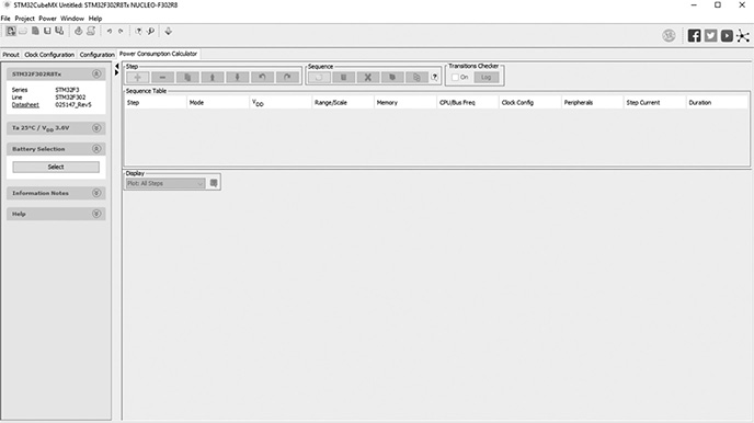
Figure 3-13 Power consumption calculator (PCC).
This PCC will allow you to calculate the following:
• Average current consumption
• Expected battery life
• Average DMIPS (Dhrystone million instructions per second): It is essentially a measure of the MCU efficiency as computed using a standardized software test
• Maximum ambient temperature (TAMAX): The maximum ambient temperature is computed based on the MCU package type, internal power consumption, and a preset 105°C maximum junction temperature
There are a series of procedural steps that are carefully detailed in the CubeMX user manual, which will lead you through a step-by-step analysis to ensure that the selected battery will handle your desired application. I will not use the PCC because all the book projects use a USB power source.
Creating an Example Project using CubeMX
It is now time to discuss how to create a new project using the CubeMX application. First start the application and then click on The New Project selection. The opening New Project screen, as shown in Figure 3-14, will be displayed.
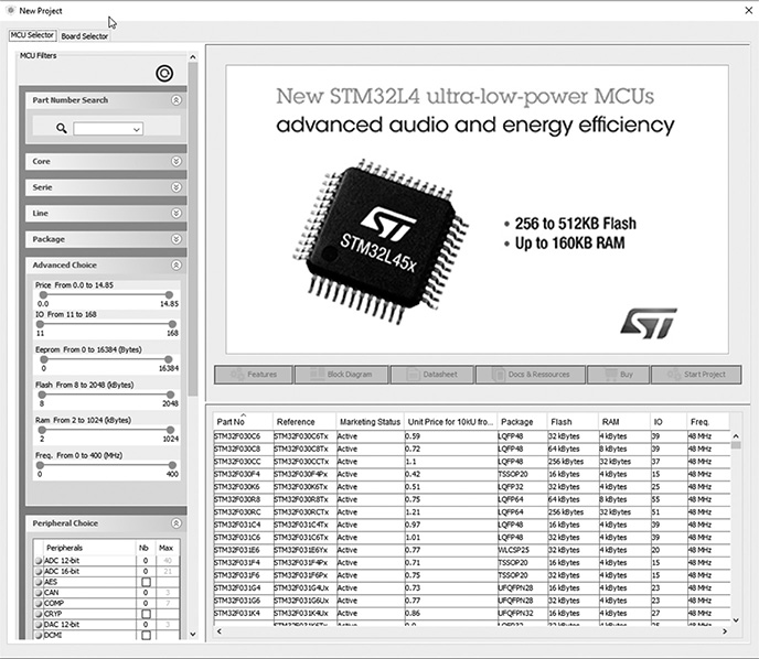
Figure 3-14 New Project opening screen.
Click on the Board selection tab, which should cause the Board Selection screen to be shown. Select your project board as I did in Figure 3-4. Double-clicking on the board selection will cause a Pinout window view to appear for the STM32F-302R8Tx MCU, as shown in Figure 3-5.
You will now need to click on the menu bar selection title Project in order to name your new project. Select Setting from the drop-down menu, which is shown in Figure 3-15.
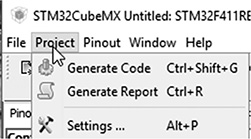
Figure 3-15 Project dropdown menu.
Figure 3-16 shows the Project Settings window that will appear after you click on the Settings selection in the Project dropdown menu.
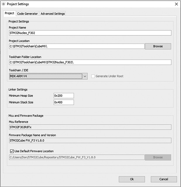
Figure 3-16 Project Settings screen.
You must first enter a name in the Project Name textbox. I used “STM32Nucleo_F302” as a project name, but you can choose anything that you like. You should ensure that the Project Location textbox displays where you desire the project folder to be stored. You can use the Browse button to find the appropriate directory. For this demonstration, I used the same location I previously used for earlier book projects. The next textbox entitled Toolchain Folder Location should be a directory named using the combination of the Project Location and the Project Name. Make note of this location because you will shortly need to access files that CubeMX will automatically create and store in it.
Next, ensure that you have selected “MDK-V4” as the Toolchain/IDE to use, as shown in Figure 3-16. This selection is very important because CubeMX cannot generate the correct C/C++ code without this being selected. In addition, ensure that the Generate Under Root checkbox is checked, which will allow the generated code to be located in the proper directories.
The default linker Settings are okay. Check that the MCU Reference textbox matches the MCU you are using. If it does not match, then the generated code cannot function with the physical MCU.
Finally, the Firmware Pack Name and Version textbox as well as the Use Default Firm Location textbox should be okay as is.
In preparation for code generation, go back and click on the Project menu bar selection and click on the Project Settings submenu selection. Next, click on the Code Generator tab and the screen shown in Figure 3-17 should appear.
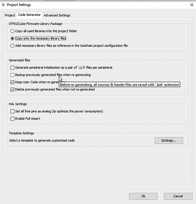
Figure 3-17 Code Generator screen.
Ensure that all the radio buttons and checkboxes are selected, as shown in Figure 3-17. You should note that I selected the radio button to “Copy only the necessary library files” in order to minimize the size of the project as stored on the host computer. Selecting the radio button “Copy all used libraries into the project folder” would have increased the overall project folder size. In either case, the final binary file size would still be the same.
Next, return to the Project submenu as has been shown in Figure 3-17, but this time click on the Generate Code selection. The CubeMX will take a few seconds to generate the code with a progress bar appearing on the screen. When the code generation is completed, you should see the informational dialog box, as shown in Figure 3-18.
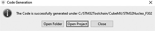
Figure 3-18 Successful code generation dialog box.
After you click the Open Project button, you have the Keil IDE main window with the STM32Nucleo_F302 project directories and files listing appearing in the IDE’s Project pane. This view is shown in Figure 3-19.
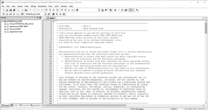
Figure 3-19 Initial STM32Nucleo_F302 project in the Keil IDE.
There should be four subdirectories in the Project pane named STM32Nucleo_F302, Application/MDK-ARM, Drivers/CMSIS, and Application/User, respectively. In Figure 3-20, I expand all the subdirectories to show you all the files contained in them.
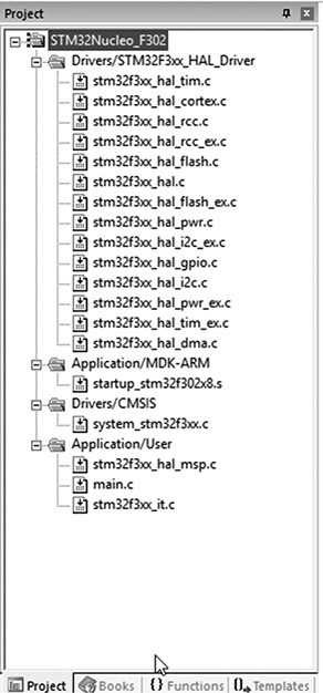
Figure 3-20 Project directory, subdirectory, and file list.
Your listing should be similar, depending upon the particular MCU that you used. Don’t be dismayed by the number of directories and files. You will only be dealing with three at most in the upcoming chapter projects.
There will also be a pop-up dialog box warning you that a device was not found. This dialog box is shown in Figure 3-21 and is simply a consequence that the initial project load did not have a specific MCU selected.
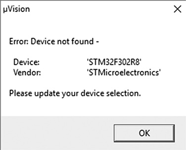
Figure 3-21 Device not found dialog box.
This is easily fixed by clicking on File → Device Database, as shown in Figure 3-22.
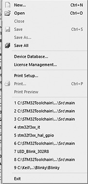
Figure 3-22 Device Database menu selection.
Next select STMicroelectronics as the manufacturer and scroll down its rather impressive list of MCUs until you find your specific model. In my case, I did not find STM32F302R8, but did find STM32F302RB, which seems to work quite well. Maybe there will be some problems in the future, but I have not encountered any to date with this selection. Figure 3-23 shows the result of the STM32F302RB selection.
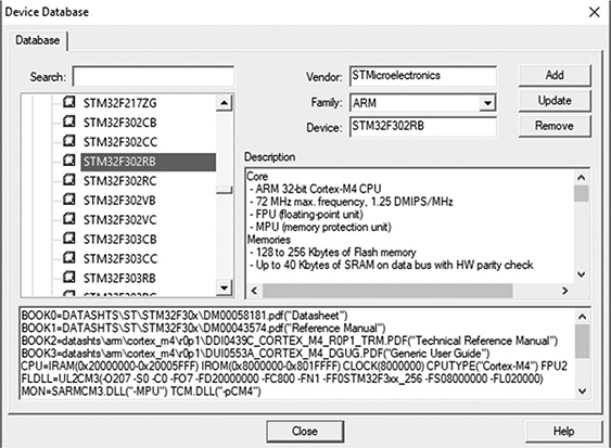
Figure 3-23 STM32F302RB selection.
Just click on the Close button because there is not a Submit or Select button.
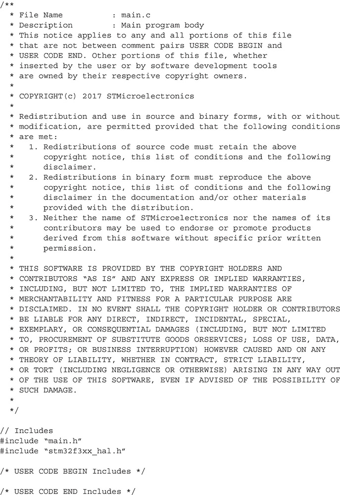
The main.c Code Listing
The following code listing is a file named main.c which was automatically generated by the CubeMX application based solely on the parameters and configuration settings that I entered. My purpose for this listing is to show you the basic template, which will constitute the bulk of the code for all the remaining projects in this book. In this listing is a method named main, which is where the majority of any functional code will be placed. In this template, it is intentionally empty because there is no functionality desired for this program. I am also required to show the voluminous STM disclaimer comments, which are part of STM’s copyright requirements to use this code. This disclaimer will be present in all the actual code examples presented in the book. However, it will not be expanded as shown in this listing. You can always click on a small + sign to display the disclaimer.
After the listing, I have provided some additional comments regarding the methods contained in the listing.
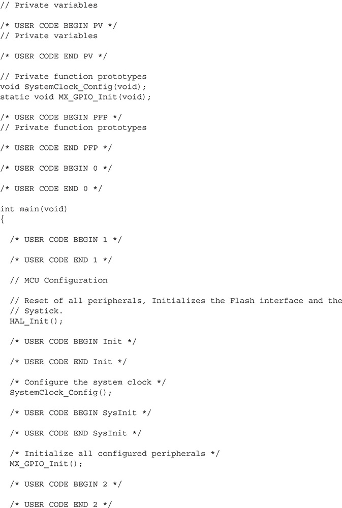
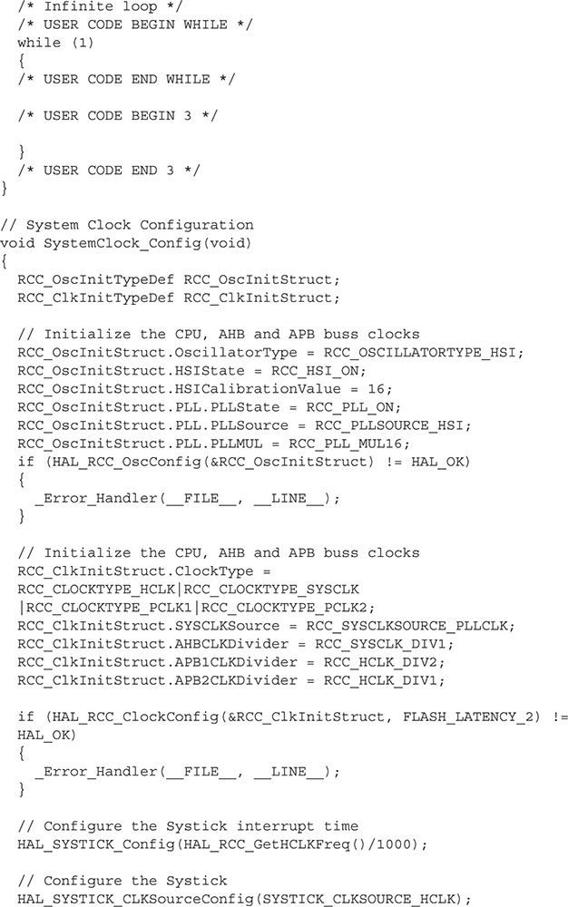
The main method, as I have previously mentioned, contains most of the functional code required by the program. The following code snippet in the main method is what I refer to as a forever loop:
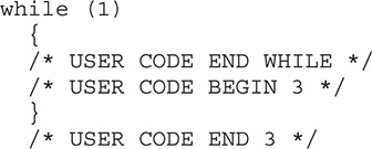
The while (1) statement causes everything contained within its scope braces to be repeated indefinitely or as I call it “forever.” This is a necessary software construct because the majority of embedded systems do not use an operating system (OS) and any running program would simply run once and then halt and likely crash. Functional code, such as for blinking an LED, would be placed in this while loop. The automatic comments generated by the CubeMX application will help guide you in placing your own code in the proper spots.
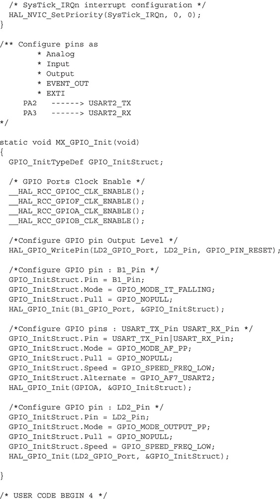
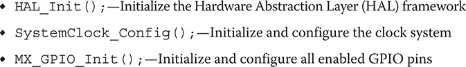
There are also a series of method calls in main that both initialize and configure the internal peripherals and GPIO pins for the MCU. These are listed in the same sequence as they are called:
There can be additional methods added to the main.c file depending upon the number and types of internal peripherals that are enabled. In addition, some extra code will have to be added to files outside of main.c to support operations such as interrupts. I will cover those cases in later chapters.
At this point, I need to discuss the ARM CMSIS software architecture in order for you to understand how the newly generated code fits in with the overall software architecture.
ARM Cortex Microcontroller Software Interface Standard (CMSIS)
ARM, which holds the intellectual property (IP) rights to all the Cortex-based MCUs, has created an interface standard that allows for efficient cross-vendor software development. This standard is called the Cortex Microcontroller Software Interface Standard and usually abbreviated as CMSIS. CMSIS addresses a full set of development tools including compilers, run-time libraries, debuggers, and other associated tools and utilities. CMSIS consists of the following main components:
• CMSIS-CORE: Standard application programming interface (API) covering the Cortex M0, M3, M4, and M7 processors and associated peripherals.
• CMSIS-Driver: Peripheral driver software interfacing all applicable devices with supported middleware software. This CMSIS portion contains items such as the file systems, communication stacks, and user interfaces.
• CMSIS-DSP: Extensive optimized library supporting different data including both fixed and floating point data types. Library is applicable to Cortex M0, M3, M4, and M7 core processors.
• CMSIS-RTOS: A standardized API implementing a real-time operating system (RTOS). This API provides a framework that supports a variety of specific Cortex, RTOS implementations.
• CMSIS-DAP: Debug access port (DAP) is a standardized set of firmware routines that implements debugging features optimized for Cortex processors. It connects to the CoreSight Debug Access Port to have rapid access to real-time data.
• CMSIS-SVD: This is an extensible markup language (XML) file named System View Description (SVD), which contains peripheral descriptions suitable for use by programming language header (include) files as well as debuggers and interrupt controllers.
• CMSIS-Pack: An XML file collection containing logical descriptions and parameters for a variety of devices. A main file named PDSC is used to extract desired data from the XML file collection.
It should be noted that the STM hardware abstraction layer (HAL), discussed in the next chapter, contains specifics only related to STM MCUs and is somewhat noncompliant with the ARM Cortex Microcontroller Software Interface Standard (CMSIS). Using the CMSIS is totally voluntary on part of vendors manufacturing ARM-based MCUs and STM has apparently decided that using HAL is the best approach in its case to handle the wide variety of MCUs and associated development boards it makes. I believe STM tried to stay compliant with the CMSIS but still needed to support its vast array of products.
CubeMX-Generated C Code
It is now time to return to a discussion of the automatically generated code that the CMSIS framework has introduced. Figure 3-24 is an interesting composite of the newly generated directories that show how they are related to the various CMSIS components.
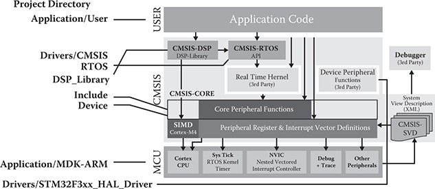
Figure 3-24 Generated code related to CMSIS structure.
The Application/User directory contains essentially skeleton files that present a framework that users can populate with specific code to implement a desired application. The files contained within these directories are only applicable to the Application block, as shown in Figure 3-24.
The Drivers/CMSIS structure contains header files with names such as core_cm3, core_cm4, and so on, which contain specific logical definitions required by the real MCU peripherals and all associated control/data registers. There are also core MCU definitions as well as interrupt controller definitions and helper functions.
The Drivers/STM32F3xx_Hal_Driver directory contains all the remaining data and parameters necessary for MCU operations not already provided in other directory files. This data covers items such as interrupt numbers, peripheral device addresses, restart vectors, and additional helper functions.
The Application/MDK-ARM contains ARM-specific startup code necessary to initialize the target MCU.
Compiling and Downloading the Project
At this point there is sufficient initialization and configuration code to build a downloadable file suitable to be run on the target. Unfortunately, it is a null project, meaning that nothing meaningful is being accomplished by the MCU. However, it is still a useful exercise to determine if the code, as it stands, can be compiled and downloaded to the target.
Figure 3-25 shows where the Keil IDE build icon is located. Clicking on this icon will start the automatic build process converting the source code in the project to a binary file.
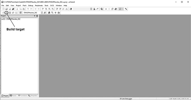
Figure 3-25 Keil IDE build icon.
Figure 3-26 shows all the intermediate results that happen during the build process. This log can be very useful in the case of errors that can happen during the build process.
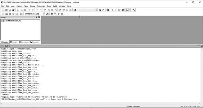
Figure 3-26 Build process log.
You may have noticed that the final compiled and linked binary file is in an axf format. This format is not compatible to be used with the ST-LINK, which expects the download file to have a hex format. This is easily fixed by clicking on the Flash menu selection and then clicking on the Configure Flash Tools. Click on the Output tab once the flash tools selection has opened. Then click on the checkbox next to the Create HEX File selection. Figure 3-27 shows this selection.
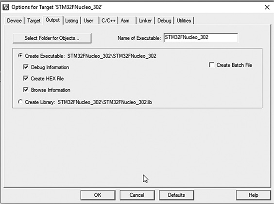
Figure 3-27 Select hex file output.
The project must be rebuilt once the hex file has been selected. This is easily done by just again clicking on the build icon. The IDE is smart enough to understand that the source code does not have to be recompiled but simply linked again to form a hex file. The resulting hex file is clearly shown in Figure 3-28.
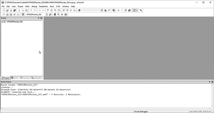
Figure 3-28 Hex file output.
The target can now be programmed once the hex file is created. The ST-LINK application is used to download the hex file into the target, as has been previously described in Chapter 2.
Downloading the Hex Code
You first need to open the ST-LINK application and open the appropriate hex file to be downloaded. The hex file is automatically placed into the project’s MDK-ARM subdirectory as part of the build process. You will have to browse to this directory using the ST-LINK open file feature found in the File menu selection. Figure 3-29 shows how the sample hex file was selected.
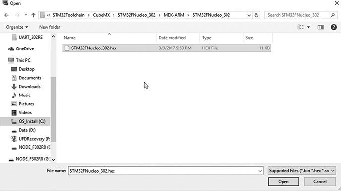
Figure 3-29 Open the hex file to be downloaded.
The target must then be connected to the host computer running the ST-LINK application using an appropriate USB cable, as has been previously discussed. You will next need to click on the Target menu selection and then click on the Connect selection. Figure 3-30 shows the ST-LINK window after the application is connected to the target.
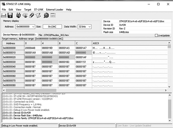
Figure 3-30 ST-LINK connected to a target.
All that’s left is to download the hex file that has been loaded into the ST-LINK application. Click on the Target menu selection and then click on the Program and Verify selection. Figure 3-31 shows the Program and Verify dialog box.
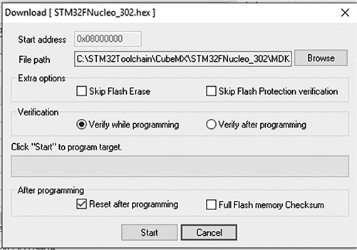
Figure 3-31 Program and Verify dialog box.
Click on the Start button to download the hex file into the target board. The red/green LED on the Nucleo board will start flashing with alternating colors to indicate that the download operation is progressing. While the download is very quick, the LED will continue to flash. I guess the STM engineers just wanted to let users know the board was programmed. Figure 3-32 shows the result of a successful download.
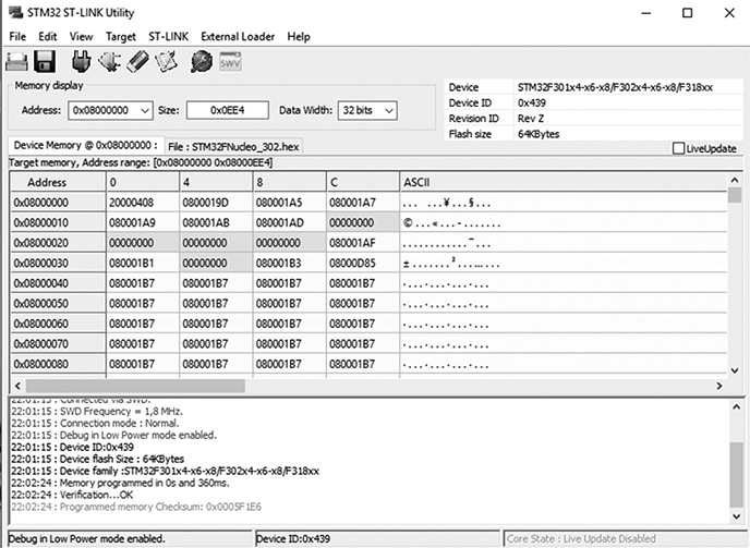
Figure 3-32 Successful hex file download.
The target board should be functioning in accordance with its program. In this case, absolutely nothing will happen because no functionality was programmed. This addition of functionality to the program will be investigated in the next chapter. However, I want to ensure that the download was okay, so I previously programmed the target to flash the user LED. Once the new hex file was downloaded, the LED stopped blinking, which indirectly confirmed that the nonfunctioning program was properly downloaded.
Summary
The chapter began with an introduction to the STM32CubeMX application, which I simply referred to as CubeMX for the remainder of the book. The application has four main portions or tabs that I thoroughly discussed. CubeMX’s purpose is to initialize and configure either STM MCUs or associated development boards, which include automatically generating C code to support the desired configuration. The automatic C code generation does not extend to any embedded application, which is still the developer’s responsibility.
A generic CubeMX project was created that did not do anything other than to provide a platform for the automatically generated C code, which supports the peripherals, clocks, communication channels, and interrupts for the specific Nucleo development board. I also presented the code contained in the main.c file and briefly discussed the contents and their operations.
I next discussed the ARM CMSIS, which most ARM vendors try to be in compliance. I also showed how the automatic C code is related to the CMSIS framework.
I showed you how to build a nonfunctioning project to prove that the toolchain works as desired. The CubeMX application created all the C code because there was no developer-responsible code required for this project. The ST-LINK application was used to download a hex file to the target platform.
The process detailed in this chapter will be repeated for all the remaining book projects, and specialized code will be added to perform all desired functions.