1
Introduction to the STMicroelectronics Line of Microcontrollers
This chapter provides you with an introduction to the very comprehensive STMicroelectronics (STM) line of microcontrollers (MCUs). I will be focusing only on several specific controllers throughout the book, but that should provide you with an adequate representation of the functions and capabilities of the full line of STM MCUs.
Microcomputer vs Microcontroller
I believe at the start of this book that it must make very clear the differences between a microcomputer and a MCU. The reason for this distinction is very simple: STM is a company that designs and manufacturers MCUs, not microcomputers. I think my following definition of a MCU is as good as any that I have read:
A microcontroller is an integrated system containing a minimum of a microprocessor, dynamic and non-volatile memory, and a set of peripherals consistent with all design requirements.
Right away, you can see from the definition that a MCU contains a microprocessor which is sometimes referred to as a microcomputer. There also must be both dynamic or volatile memory as well as nonvolatile or static memory, where the latter holds any programs or scripts necessary to run the microprocessor. Finally, there are always peripherals added to the design that allow for the input and output of digital signals. There are often additional peripherals such as timers, interrupt controllers, serial data ports, and a variety of others depending upon what requirements the MCU must meet.
I discuss all the principal MCU components below to provide you with a solid background to understand how a MCU functions. Most of the following explanations are based on the voluminous amount of information provided by STM on their microcontrollers. The reason behind STM providing such a large amount of information is to allow engineers/software developers access to all the data they need in order to incorporate STM products into original equipment manufacturer (OEM) designs and products. This approach is fundamentally different than the approach taken by suppliers of maker style boards and products, such as the Arduino, Raspberry Pi, BeagleBone, and so forth. In the case of the latter, board documentation is geared toward how to use a board in a project. The STM data is extremely specific describing items such as the nanosecond timing pulses between memory chips and processor buses. This is exactly the reason why some of the STM MCU datasheets are over 1,100 pages in length. Fortunately, the datasheet for the primary STM MCU I will be using in this book is only 138 pages. I will provide later in this chapter the website where you can download the datasheet.
STM Nucleo Boards
MCU manufacturers such as STM have long recognized that they just couldn’t provide only chips to potential customers as most would have no way to effectively evaluate them for potential use in their products. This is the reason why the manufacturers offer relatively low-cost evaluation and demonstration boards, which have representative MCUs all setup and ready to run. STM offers a series of such boards that it calls the Nucleo line. I will be using a fairly simple Nucleo-64 board for the book projects. STM has actually embraced the maker community by marketing the Nucleo lineup as boards suitable for maker project use. These boards are very inexpensive, usually about US$10–15, which leads me to believe that STM is striving to gain a foothold in the maker community by actually subsidizing the manufacturing costs for the boards. In any case, this is a boon for makers and hobbyists and one that we should embrace.
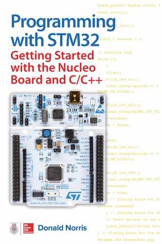
Figure 1-1 shows the three basic Nucleo boards available at the time of writing this book.
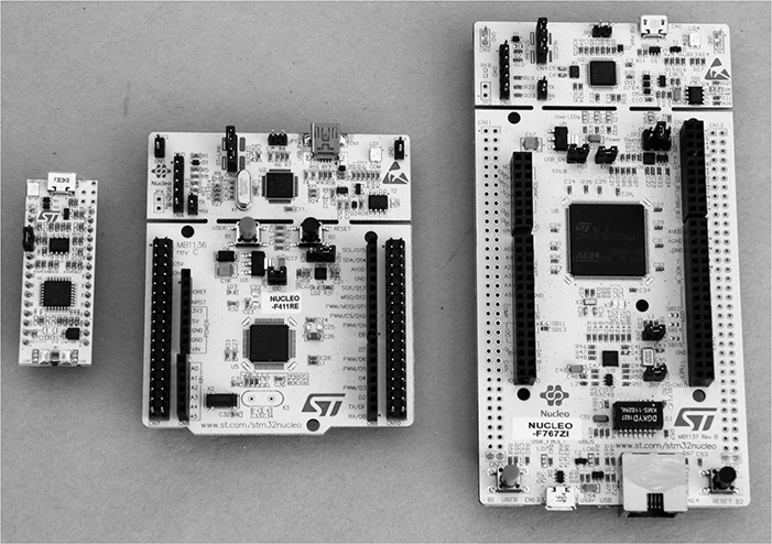
Figure 1-1 Three basic Nucleo boards.
The boards are named Nucleo-32, Nucleo-64, and Nucleo-144 from left to right, respectively, as shown in Figure 1-1. The number in each name represents the number of pins present in the MCU chip. Nucleo-64 is the principal board used in this book.
Principal MCU Components
The first component to consider is the processor or microcomputer.
Processor
The processor used in Nucleo-32 and Nucleo-64 boards is the ARM Cortex M-4 32-bit processor. It too has a lengthy 278-page user guide available from infocenter.arm.com/help/topic/com.arm.doc.dui0553a/DUI0553A_cortex_m4_dgug.pdf. The actual processor circuitry is part of the STM MCU because STM has purchased intellectual property (IP) rights from the ARM Corporation in order to integrate it into its chips. However, for all practical purposes, the ARM processor is programmed using the tools and techniques promulgated by the ARM Corporation to support its processor IP. This distinction is of no consequence in our case because the software tools to be used for the book projects have all been carefully crafted and tested to work seamlessly together by STM. Any license issues have already been resolved without bothering the end user.
The following list contains some of the important specifications for the Cortex M-4 processor for interested readers:
• Full-featured ARMv7-M instruction set, optimized for embedded applications
• Floating point unit (FPU)
• Low-power 32-bit processor
• Memory protection unit (MPU)
• Nested vector interrupt controller (NVIC)
• Trace, breakpoint, and JTAG capabilities
• Advanced Microcontroller Bus Architecture (AMBA)
• Advanced High-Performance Bus (AHB5, AHB-Lite)
There are many more features to the Cortex M-4 processor as the 278-page user guide would suggest. I would also recommend Joseph Yiu’s book, The Definitive Guide to ARM® Cortex®-M3 and Cortex®-M4 Processors, Third Edition, to readers who really want to delve into this processor to a great depth.
Figure 1-2 is a block diagram of the Cortex M-4 processor showing all of the listed items and more.
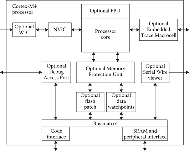
Figure 1-2 ARM Cortex M-4 block diagram.
STM is responsible for the design and implementation of all components outside of the box shown in Figure 1-2. Of course, the STM design must be compliant with the ARM processor specifications. One item missing in the figure is a clock input. The reason for it being missing is that the block diagram is from the ARM Cortex M-4 user guide, while the clock circuitry is the responsibility of STM, the MCU designer. STM has set the base processor clock frequency at 72 MHz, which appears to be very low in today’s world of multi-gigahertz clock rates for most PCs. In fact, the latest Raspberry Pi model 3 has a 1.2-GHz clock rate. But first appearances are deceiving in this case. The Cortex M-4 processor uses an extremely efficient instruction set, with three-stage pipelining, which maximizes the performance of the underlying reduced instruction set computing (RISC) that the processor employs. In addition, many common microcontroller tasks, which I discuss below, have been implemented in a combination of hardware and firmware, further improving the overall performance, while keeping the power consumption as low as possible. Power consumption and performance are two key microcontroller attributes that system designers always keep in mind. Keeping the clock rate as low as possible will always minimize the power consumed as well as increase the longevity of the chip.
Memory
The Cortex M-4 processor uses a Harvard architecture. This means that program instructions are stored and retrieved from a memory separate and distinct from the memory that holds data. The other common computer architecture is named von Neumann in which instructions and data share a common memory. MCUs have very limited memory and take advantage of the speed-up available by using concurrent instruction and data access. Additionally, having separate memories means that the processor is no longer constrained to the same sized data widths. This means instructions can be fetched and executed in 4-byte chunks or 32 bits, while data can be simultaneously handled with 1-byte or 8-bit chunks, thus speeding up the overall throughput to and from the processor and memory. Another advantage the Harvard architecture has over the von Neumann form is that instruction prefetches can now be done in parallel with regular instruction executions, thus further speeding up the overall system performance. Finally, concurrent instruction and data access eliminates the need for data caches, which are typically used in von Neumann machines. This further reduces system complexity and power consumption.
The Nucleo-64 board used in this book is the STM MCU, model number STM32F302R8. This chip has a 64-KB flash memory and a 16-KB static random access memory (SRAM). Yes, those are kilobytes, not mega- or gigabytes. You cannot expect to create any graphical programs that run in this limited memory space. Microcontroller programs are truly a throwback to the earliest days of computing where memory was very limited and developers had to use every available byte to store and execute programs. Having mentioned the scarce memory resources, you will be able to use a variety of modern-day graphic-based programs to develop the MCU program, but they will run on a PC. The compiled and optimized binary code will be downloaded into the MCU from the PC.
It turns out that 64 KB is plenty of space to run fairly large programs because the C/C++ cross-compiler used for this book’s projects produces optimize code, eliminating all but the essential instructions needed for the program. The 16-KB SRAM size is more than adequate for the dynamic memory requirements to support a maximum 64-KB sized program. The actual memory is integrated onto the MCU chip and its type is largely irrelevant for our purposes.
Peripherals
The peripherals are what make the MCU viable for its intended purposes. In my microcontroller definition I stated, “a set of peripherals consistent with all design requirements.” This means that microcontrollers typically have different peripheral configurations depending upon the requirements they are designed to meet. This is a major reason why STM manufactures such a wide variety of MCUs. I will focus on the Nucleo-64 microcontroller I mentioned above and will use its set of peripherals as my discussion points. I will next need to demonstrate how the Nucleo-64 board is set up in order to fully explain how all the peripheral features function with this board.
Nucleo-64 Board Layout
Figure 1-3 is a block diagram showing how the major components that make up a Nucleo-64 board are configured.
Figure 1-3 Nucleo-64 block diagram.
The first item you should note is that the board is actually made of two sections, the top section being a ST-LINK/V2-1 programmer and the bottom section is the STM32 MCU. The bottom section is also fitted with two sets of connectors. One set is compatible with the Arduino shield pin configuration and other set is the ST Morpho pinout configuration. There are two push buttons, B1 and B2, shown in the figure. B1 is multipurpose, while B2 is the reset push button. There is also one LED indicated in the figure; however, there are several others also which are shown in follow-on figures. The programmer section may be separated from the microcontroller section by snapping the sparse printed circuit board (PCB) joints, which can be seen in Figure 1-1. I would not recommend doing so because you would lose all programming capability for the MCU section. I suppose it was set up in this fashion so you could separate the sections once there was a working MCU for a specific project and there was no need for any further programming.
Figure 1-4 is a top view of the Nucleo-64 board with most of the components clearly annotated.
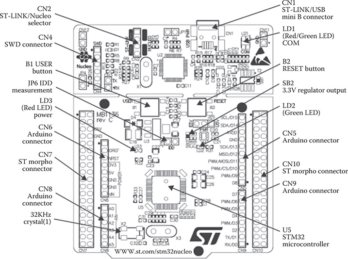
Figure 1-4 Annotated top view of the Nucleo-64 board.
Remarkably, there are relatively few components on the board. Most of the space is taken up by connectors, push buttons, configuration jumpers, LEDs, and the microcontroller chip. This sparse layout reflects the nature of the MCU, which is to be an embedded device without any of the niceties needed for the human-computer interface (HCI). HCI is possible with this board by using an appropriate extension board that plugs into this board
Figure 1-5 shows the bottom side of the Nucleo-64 board.
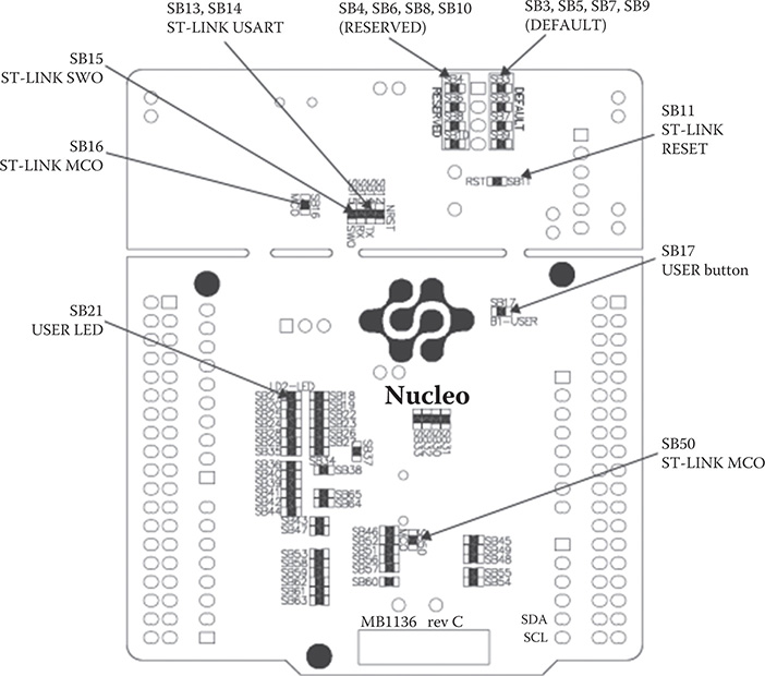
Figure 1-5 Annotated bottom view of the Nucleo-64 board.
Not much to see in this figure other than a bunch of 0-ohm resistors that may be removed if it was desired to disable certain features such as the reset and user buttons and user LED, or make hardware configuration changes to the ST-LINK programmer.
Figure 1-6 is much more interesting as it shows the pinouts for all the connectors on the top of the Nucleo-64 board.
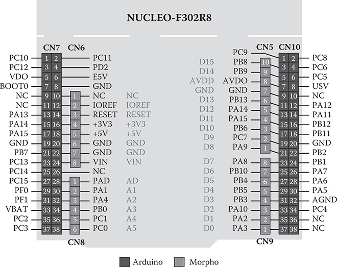
Figure 1-6 Nucleo-64 pinout diagram.
There are two sets of pinouts shown in Figure 1-6, one belonging to the Arduino and the other to the ST Morpho. Connectors CN5, CN6, CN8, and CN9 belong to the Arduino set. Connectors CN7 and CN10 belong to the Morpho set. It is important to note that there are no one-to-one relationships between the sets. The Morpho connectors are two double rows of 38 pins for a total of 76 pins. The Arduino connectors are single-row connectors totaling 32 pins in all spread across four connectors.
Arduino Connectors
Tables 1-1 to 1-4, which are from the Nucleo-64 User Guide, detail the Arduino connectors with cross-references between Arduino pin terms and STM32 pins. I have provided further clarifications on some of the pin functions following each table, where I felt it was appropriate.
Table 1-1 details the CN6 connector pinout. Refer to Figure 1-4 to see the placement of CN6 on the board.
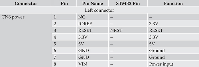
Table 1-1 CN6 Pinout
Grounding pin 3 will reset the MCU. The STM32 pin designation NRST is short for non-maskable reset, which means a low on this pin is always recognized as a forcible MCU reset. Pins 2 and 4 provide 3.3 V, but I would recommend that only a very limited amount of current be drawn from these pins or you risk disrupting the board operations. Pin 5 provides 5 V, but again my same caution exists for excessive current draw. VIN is where you can attach an external power supply. The input voltage range is approximately 7 to 12 V based on the voltage regulator ratings connected to this pin. Jumper JP5 must be switched to accommodate the external power supply. Finally, the IOREF pin allows Arduino shields to adjust the I/O voltage to the 3V3 for the STM32 if those shields follow the STM specification.
Table 1-2 details the CN8 connector pinout. Refer to Figure 1-4 to see the placement of CN8 on the board.
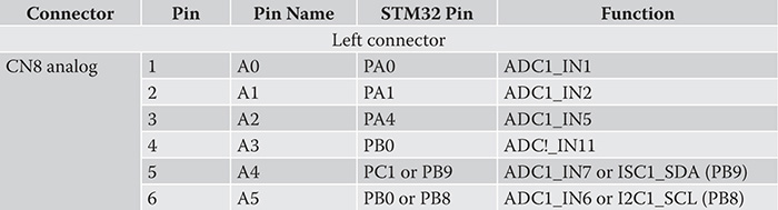
Table 1-2 CN8 Pinout
These pins are the analog voltage inputs that are routed to the MCU multichannel analog-to-digital converter (ADC). You must restrict the analog input voltage to 3.3 V or less to avoid damaging the ADC inputs. Note that there is no one-to-one correspondence between the Arduino channels and the MCU channels. Pins 5 and 6 are the default ADC inputs. If you need these to bus #1 I2C inputs, you must disconnect solder bridges SB51 and SB56 and connect SB42 and SB46. These connections are made using 0-ohm resistors on the bottom side of the MCU board. Please note that the bus #1 I2C connections are already available on pins 1 and 2 on connector CN5.
Table 1-3 details the CN5 connector pinout. Refer to Figure 1-4 to see the placement of CN5 on the board.
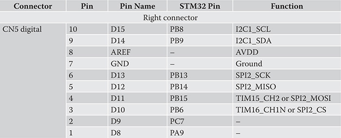
Table 1-3 CN5 Pinout
The analog voltage reference (AREF) should be connected to 3.3 V because that is the maximum allowed voltage to be input to the MCU ADC channels. If you have another supply available with a lesser voltage, say 2.5 V, then you can connect AREF to that and increase the ADC dynamic range by a third. Just be aware that inputting a voltage greater than 2.5 V will not change the ADC output, effectively saturating it. Pins 3 to 6 may be configured as general-purpose input/output (GPIO) or act as the bus #2 serial peripheral interface (SPI). Pins 2, 3, and 4 can also act as timer pins if neither the GPIO nor the SPI is required.
Table 1-4 details the CN9 connector pinout. Refer to Figure 1-4 to see the placement of CN9 on the board.
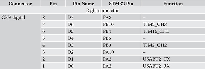
Table 1-4 CN9 Pinout
These eight pins are normally regular GPIO, but they may be reconfigured so that pins 4, 6, and 7 are timer pins. In addition, pins 1 and 2 can act as the #2 USART.
Morpho Connectors
Table 1-5 is from the Nucleo-64 User Guide and details the STM Morpho connections with references to the STM32 pins. I have provided further clarifications on some of the pin functions following the table, where I felt it was appropriate. I did not repeat the comments I provided for Arduino connection as they are equally valid for the Morpho connections.
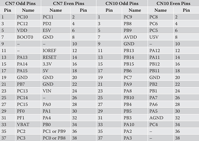
Table 1-5 CN7 and CN10 Pinouts
Table 1-5 details the CN7 and CN10 connector pinouts. Refer to Figure 1-4 to see the placement of CN7 and CN10 on the board.
U5V is 5-V power supplied from the ST-LINK/V2-1 USB connector. The BOOT0 input pin allows for changing how the MCU initially boots during a power-on event. I will discuss the boot options in a later chapter. VBAT input is often used as a battery backup for powering a real-time clock or a security key. It is typically tied to VCC if not used for a battery backup.
The next series of MCU components that I will discuss enable the MCU to perform its operations more efficiently and quickly than possible by relying on software constructs.
Nested Vectored Interrupt Controller (NVIC)
Interrupts are essential elements in the MCU structure. Without them, MCUs cannot efficiently function given the limited memory available and low clock speeds. MCU interrupts are implemented both in hardware and software. But first I need to define what an interrupt is and how it is used:
An interrupt is a disruption in the normal flow of a program initiated by an external or temporal event.
Figure 1-7 is a flow diagram of a generic interrupt sequence. This diagram will make it easier to understand how an interrupt works.
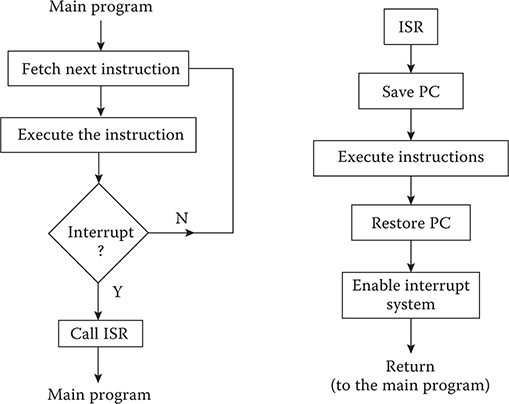
Figure 1-7 Interrupt flow diagram.
ISR in Figure 1-7 stands for interrupt service routine, which is the program code that executes whatever needs to be accomplished due to the interrupt. The block containing the phrase “Call ISR” causes the current state or context of the MCU to be saved in SRAM. The current state typically consists of the contents of program counter (PC) and a preset number of registers that depends on the MCU model. The PC is a register, which contains the address of the next instruction to be executed when the interrupt was recognized. The actual ISR code may be located anywhere in memory because it is accessed by replacing the PC with the first address of the ISR. That address is contained in a list, which is known as the vector interrupt list. The last instruction in an ISR is always a return from interrupt, which restores the MCU’s pre-interrupt state and resumes executing instructions at the stored PC address.
The figure is slightly off target and shows a block in the ISR section containing the phrase “Enable interrupt system.” The STM NVIC uses prioritized interrupts, which means a higher priority interrupt can always interrupt a lower priority interrupt while it is executing. This normally is not possible with a purely software-implemented interrupt scheme, which is depicted by the figure’s flow diagram.
Figure 1-8 shows two ways the NVIC handles multiple interrupt requests (IRQs).
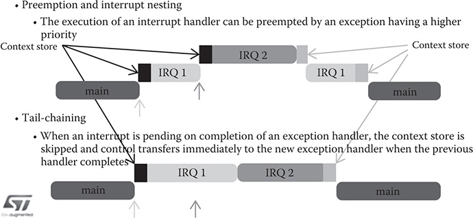
Figure 1-8 NVIC handling multiple IRQs.
I don’t believe it makes much difference on how the NVIC handles interrupts for most non-safety-related projects. However, it would be very important if a designer was creating a safety critical system. One case that came to mind was an automotive control system, in which a STM MCU was managing a variety of systems including the infotainment system and a collision avoidance system. I certainly think that a collision avoidance IRQ would need immediate attention if the MCU was processing a radio station change request at the time the higher priority IRQ was received.
The NVIC used in the Nucleo-64 MCU project board has the following specifications:
• Sixteen interrupt lines
• Sixteen priority levels
• Up to 62 maskable interrupt channels
• Low-latency interrupt processing
• Processing of late arriving, higher priority interrupts
• Supporting tail chaining
• Interrupting entry restored on interrupt exit with no instruction overhead
I will discuss how to program ISRs in the software chapter.
General-Purpose Inputs/Outputs (GPIOs)
Each of the 51 GPIO pins can be configured by software as output with push-pull or open-drain and with or without pull-up or pull-down. They can also be configured as floating input, with or without pull-up or pull-down. Most GPIO pins have peripheral alternate functions as can be seen in the above tables. All GPIOs are high-current-capable and have limited speed selection to better manage internal noise, power consumption, and electromagnetic emission.
Analog-to-Digital Converter (ADC)
There is one 12-bit ADC that has 16 channels. ADC conversions can be done in either a single-shot or scan mode. In the scan mode, an automatic conversion is performed on a preselected group of analog inputs. An interrupt can be generated if a converted voltage is outside preset threshold. In addition, a specific channel conversion can be triggered by the TIM1, TIM2, TIM3, TIM4, or TIM5 timers.
External Interrupt/Event Controller (EXTI)
There is an external interrupt/event controller that uses 23 edge-detector lines to generate interrupt/event requests. Each line may be independently configured to select the trigger event such as leading edge, trailing edge, or both. All these lines can be independently masked. There is a register that maintains the status of each interrupt request. The EXTI can detect an external line with a pulse width shorter than the internal main clock period. Up to a maximum of 81 GPIOs can be connected to the 16 external interrupt lines.
Timers and Counters
Many typical MCU activities involve temporal or timing events. Using hardware timers and counters can minimize software execution cycles that are best allocated to other activities. That is why MCUs typically incorporate an array of timers and counters in their structure. Timers and counters are also tightly coupled with interrupts to provide an extremely efficient way to process timing and counting events.
Table 1-6 details the features supported by a single advanced control timer as well as the general purpose (GP) and basic timers.
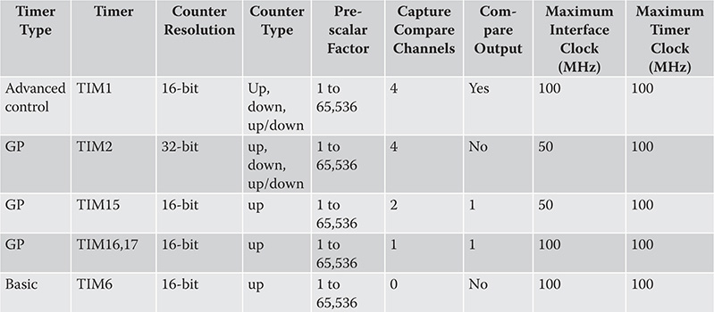
Table 1-6 MCU Timer Features
Although there are two more watchdog timers, they are not listed in the table. I discuss each timer type below.
Advanced Control Timer (TIM1)
This timer has four independent channels that may be used for the following:
• Input capture
• Output capture
• Pulse width modulation (PWM)
• Single pulse output
It can be used as a GP 16-bit timer if desired; however, the PWM mode is especially useful for the control of standard and continuous rotation servos. This timer may also be linked with the GPx timers for event synchronization and chaining.
General-Purpose Timers (TIMx)
There are four GP timers available for use. These timers, TIM2, TIM15, TIM17, and TIM16, are full-featured timers with 16-bit prescalars. TIM2 is the only 32-bit timer, while the rest use 16 bits. All of these timers, except for the basic, have up to four channels for the following:
• Input capture
• Output compare
• PWM
• Single pulse output
These timers can work together in a linked manner and they can also link with TIM1.
Basic Timer (TIM6)
The remaining timer is TIM6, which is a basic 16-bit type. It has limited options and is used only for the most basic timing feature as its name implies.
Watchdog Timers
There are two watchdog timers. The first is an independent 12-bit, count-down with an 8-bit prescalar. It is driven by a separate 32-KHz crystal, which allows it to operate independently from the main MCU clock. It also operates when the MCU is in the standby or even stop mode. This allows it to reset the MCU if an event happens that inadvertently stops the MCU.
The second watchdog timer is a free-running 7-bit downcounter that can also be set up to reset the MCU in case a problem occurs. This watchdog runs from the MCU main clock, but it does have an early-warning interrupt capability, which gracefully stops the MCU in case of an unanticipated problem.
SysTick Timer
There is one more timer, SysTick, but it is not recommended to use. This timer is ordinarily dedicated to support real-time operating systems (RTOS). However, if the MCU project is not using an RTOS, then the timer is freely available. This timer features the following:
• A 24-bit downcounter
• Autoreload capability maskable system interrupt generation when the counter reaches 0
• Programmable clock source
I would say that this timer should only be used as a last resort in the unlikely case that all the other timers have been fully committed. I cannot conceive of a project complex enough where this would happen.
Bit Serial Ports
This MCU supports 4-bit serial protocols that allow for serial communication between it and other computing systems or peripherals.
USART Serial Protocol
The first bit-serial protocol to be discussed is the standard Universal Synchronous/Asynchronous Receiver/Transmitter (USART). This serial protocol may or may not require a clock signal depending upon if it is configured as synchronous or not. The MCU provides two USART terminal ports; however, only one named USART2 is active and it is directly connected to another USART port on a separate MCU located on the ST-LINK portion of the Nucleo-64 PCB. There is also pin pair CN3 located on the ST-LINK that exposes the TX and RX lines.
It is possible to disconnect the USART2 link by opening solder bridges SB13 and SB14 and closing solder bridges SB62 and SB63. If this is done, then the USART2 port on the main MCU using pins PA2 and PA3 would be connected to CN9, pins 1 and 2, as well as to CN10, pins 35 and 37, respectively. This would then provide a USART port to any compatible serial device located on an extension board.
A second USART port named USART3 can be enabled by using jumper wires between the ST Morpho connectors CN7 and CN3, located on the ST-LINK. For example, on this Nucleo-64 board it is possible to use USART3 available on PC10 (TX) and PC11 (RX). Two jumper wires would need to be connected as follows:
• PC10 (USART3_TX) available on CN7 pin 1 to CN3 pin RX
• PC11 (USART3_RX) available on CN7 pin 2 to CN3 pin TX
While this physically restores the USART link, I am fairly sure that the underlying ST-LINK communications software would have to be modified to use this new USART port number.
I2C Serial Protocol
The second bit-serial protocol is the Inter-Integrated Circuit interface or I2C (pronounced “eye-two-cee” or “eye-squared-cee), which is also known as a synchronous serial data link. A clock signal is needed because it is synchronous. Figure 1-9 is a block diagram of the I2C interface showing one master and one slave. This configuration is known as a multidrop or a bus network.
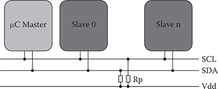
Figure 1-9 I2C block diagram.
I2C supports more than one master as well as multiple slaves. This protocol was created by Philips in 1982 and is a very mature technology, meaning it is extremely reliable. Only two lines are used: SCLK for serial clock and SDA for serial data.
The STM MCU implements three separate I2C buses. These buses can operate at the standard clock rate of 100 KHz and the fast rate of 400 KHz. This clock rate can be increased by the manufacturer to a nonstandard 1 MHz. However, that would make the I2C implementation noncompliant with the protocol. Table 1-7 shows the Nucleo-64 pin designations for bus 1 clock and data lines.
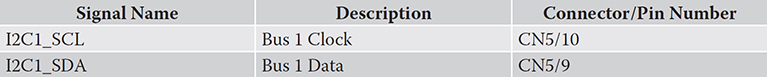
Table 1-7 I2C Signal Lines
SPI Serial Protocol
The third bit-serial protocol that I will discuss is the Serial Peripheral Interface (SPI), which is shown in Figure 1-10.
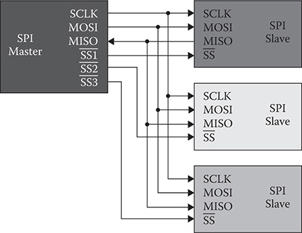
Figure 1-10 SPI block diagram.
SPI (pronounced “spy” or “ess-pee-eye”) is also known as a synchronous serial data link. It is also a full duplex protocol, meaning data can be simultaneously sent and received between the host and slave. SPI is also referred to as a Synchronous Serial Interface (SSI) or a 4-wire serial bus.
The MCU supports five SPI links in slave and master modes using full-duplex and/or simplex communication. The interfaces are labeled SPI1 to SPI5 and can use a clock rate of up to 25 Mbits/s. The data may be framed in either a byte or double-byte format. There is also automatic error correction in the form of CRC generation and verification.
Table 1-8 shows the Nucleo-64 pin designations for SPI2.
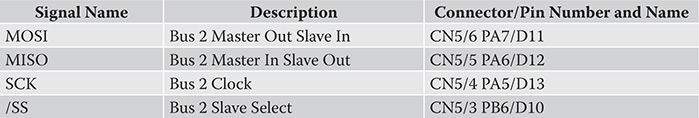
Table 1-8 SPI2 Signal Lines
Inter-Integrated Sound
The fourth and final bit-serial interface to be discussed is the inter-integrated sound (I2S) interface. There are five standard I2S interfaces that are multiplexed with SPI1 to SPI5. I2S2 and I2S3 may be operated in a master or slave mode, in either simplex or full-duplex communication modes, and can be configured to operate with a 16/32-bit resolution as an input or output channel. All I2Sx interfaces can have audio sampling frequencies from 8 kHz up to 192 kHz. Finally, the master I2S clock can be output to the external DAC/CODEC at 256 times the sampling frequency when either I2S2 or I2S3 interface is configured in a master mode.
The above discussion is simply informational because I will not be demonstrating the I2S interface.
Nucleo-64 Board Options
The following sections discuss options specific to the Nucleo-64 board and are presented to provide you with some options when working with the board.
LEDs
LD1 is a tricolor LED located on the ST-LINK PCB and provides information concerning the state of communications between the ST-LINK, the host PC, and the main MCU. The following list shows the various LED states and the corresponding meaning:
• Slow blinking Red/Off: at power-on before USB initialization
• Fast blinking Red/Off: after the first correct communication between the PC and ST-LINK/V2-1 (enumeration)
• Red LED On: when the initialization between the PC and ST-LINK/V2-1 is complete
• Green LED On: after a successful target communication initialization
• Blinking Red/Green: during communication with target
• Green On: communication finished and successful
• Orange On: communication failure
LD2 is a green LED-labeled user and connected to Arduino signal D13 (CN5/CN6), which corresponds to STM32 I/O PB13
• When the I/O value is HIGH, the LED is on
• When the I/O value is LOW, the LED is off
LD3 is a red LED that indicates that the Nucleo-64 board is powered on and 5-V power is available.
Push Buttons
There are two push buttons on the board:
• B1 USER: The user button is connected to the I/O PC13 (CN7/23) of the MCU. This pin is pulled high through a 47K resistor. When B1 is pressed the pin is grounded.
• B2 RESET: This push button is connected to NRST, and is used to RESET the MCU.
NOTE The blue and black plastic hats that are placed on the push buttons can be removed if necessary, for example, when a shield or when an extension board is plugged on top of the Nucleo-64 board. This will avoid pressure on the buttons and consequently a possible permanent target RESET.
JP6
Jumper JP6 is labeled IDD and is used to measure the MCU current by removing the jumper and connecting an ammeter in series with the two pin leads.
• Jumper ON: MCU is powered (default).
• Jumper OFF: An ammeter must be connected to measure the MCU current. The MCU cannot receive any power if there is no ammeter connected.
OSC Clock
There are four options on how to connect an high-speed external clock (HSE) on the Nucleo-64 board.
Master Clock Output from the ST-LINK (Default)
The master clock output (MCO) is generated by an 8-MHz crystal located on the ST-LINK PCB and input into the main MCU via the PF0/PD0/PH0-OSC_IN pins. This crystal frequency is fixed. Incidentally, the 72-MHz clock rate I mentioned earlier in this chapter is generated by using a phase-locked loop (PLL) embedded in the MCU using the 8-MHz input clock signal.
HSE Oscillator On-board with the Optional X3 Crystal
An 8-MHz crystal must be installed in empty X3 PCB pads. In addition, there are some solder bridges to be changed, and some resistors and capacitors to be added. The details are specified in the user’s guide.
External Oscillator Through Pin 29 of the CN7 Connector
There are some solder bridges to be changed, and some resistors to be removed. The details are specified in the user’s guide.
HSE Not Used
PF0/PD0/PH0 and PF1/PD1/PH1 are used as GPIOs instead of as a clock source. There are some solder bridges to be changed, and some resistors to be removed. The details are specified in the user’s guide. I am unsure how the MCU functions without an HSE, but it is an option according to the user’s guide.
OSC 32-kHz Clock Supply
There are three ways to configure the pins corresponding to low-speed external clock (LSE).
LSE On-board Oscillator
You can change the X2 crystal provided that it conforms to the oscillator design guide for STM32 MCU. The default crystal already installed is a model ABS25-32.768KHZ-6-T manufactured by Abracon Corporation.
External Oscillator Through Pin 25 of the CN7 Connector
There are some solder bridges to be changed, and some resistors to be removed. The details are specified in the user’s guide.
LSE Not Used
PC14 and PC15 are used as GPIOs instead of the LSE source. There are some solder bridges to be changed, and some resistors to be removed. The details are specified in the user’s guide. I am fairly sure that the real-time clock and watchdog timers will become inoperative with the LSE disabled.
Power Supply and Power Selection
I have already discussed on where an external power supply may be attached in the Arduino connector. However, there are still some more power supply features and options you should know about.
Power Supply Input from the USB Connector
The whole Nucleo-64 board including any attached extension board can be powered by the 5-V power supplied through the CN1 USB connector provided the host USB device complies with the USB standard of providing 500 mA. The ST-LINK requires 100 mA and the main MCU requires 300 mA, which leaves 100 mA for any extension board or external devices such as LEDs or LCD displays. You must use an external supply if the total current is planned to exceed a nominal 500-mA load. The red LED LD3 will not light if there is insufficient current present to power the MCU.
When the board is power supplied by USB (U5V), a jumper must be connected between pins 1 and 2 of JP5.
Jumper JP1 is configured according to the maximum current consumption of the board when powered by the USB (U5V) connection. JP1 jumper can be set in case the board is powered by USB and maximum current consumption on U5V does not exceed 100 mA (including an eventual extension board or Arduino shield). In such condition, the USB enumeration will always succeed since no more than 100mA is required from the host. Possible configurations of JP1 are summarized in Table 1-9.
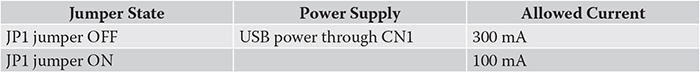
Table 1-9 JP1 Configuration Table
NOTE If the Nucleo-64 board is powered by an USB charger, there will be no USB enumeration from the ST-LINK causing the LD2 LED to remain off. In this case, JP1 needs to remain in place so that the MCU can be powered on.
VIN and E5V External Power Supply Inputs
The details and limitations of external power sources VIN and E5V are summarized in Table 1-10.
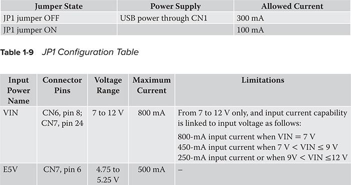
Table 1-10 VIN and E5V External Supply Input Limitations
When the board is power supplied by VIN or E5V, these jumper configurations must be set as follows:
• Jumper on JP5 pins 2 and 3
• Jumper removed on JP1
3.3-V external Power Supply Input
It is possible to power the MCU with an external 3.3-V power supply. The power connection would be made at CN6, pin 4 or CN7, pins 12 and 16. In this situation the 3.3-V supply is coming from an extension board. The ST-LINK will not be powered on with this configuration, thus making programming and debugging unavailable. The 3.3-V external power supply configuration is summarized by Table 1-11.
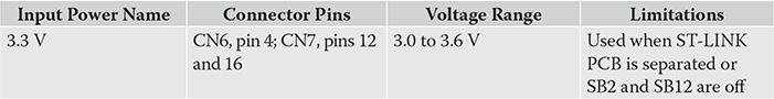
Table 1-11 3.3-V External Power Supply Configuration
External Power Supply Output
When powered by USB, VIN, or E5V, the 5-V supply (CN6, pin 5 or CN7, pin 18) may be used as output power supply for an Arduino shield or an extension board. In this case, the maximum current of the power source specified in Table 1-10 must be respected. The 3.3 V (CN6, pin 4 or CN7, pins 12 and 16) can be used also as power supply output. The current is limited by the maximum current capability of the regulator U4 (500 mA max).
Table 1-12 details the position of the JP5 jumper with regard to using an external power supply.
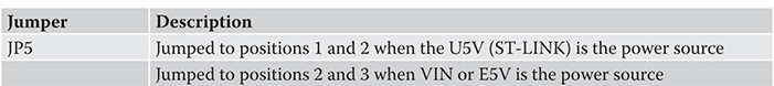
Table 1-12 JP5 Jumper Positions
Using VIN or E5V as an External Power Supply
VIN or E5V can be used as an external power supply in case the current consumption of Nucleo-64 and the extension board exceeds the maximum allowed current provided by the USB connection. It is still possible to use the USB for programming and debugging only, but it is mandatory to power-on the Nucleo-64 board first using VIN or E5V and then connect the USB cable to the host PC. Following this sequence ensures that the USB enumeration will occur when connected to an external power source.
The following power-on sequence procedure should be used:
1. Connect the jumper between pins 2 and 3 of JP5
2. Check that jumper JP1 is removed
3. Connect the external power source to VIN or E5V
4. Turn-on the external power supply VIN or E5V
5. Check that LD3 is turned on
6. Connect the host PC to USB connector, CN1
If this order is followed, the board may be supplied by VBUS first and then by VIN or E5V. The following risks may be encountered:
• The host PC USB power supply can be damaged if more than 300 mA is drawn by the Nuclueo-64 board and host cannot supply it.
• Up to 300 mA may be drawn from the host PC USB connection because JP1 is in the off position. If the host cannot supply this amount, the USB enumeration will fail and the MCU will not start.
This section concludes this introductory chapter for the STM32 Nucleo-64 board.
Summary
This is an introductory chapter on the STMicroelectronics (STM) Nucleo-64 microcontroller (MCU) development board. This board features the model STM32F302R8 MCU, which runs at 72-MHz clock rate and has 64-KB flash and 16-KB SRAM memories.
I first reviewed the differences between a microcomputer and a MCU. A review of the principal components that make up a MCU followed next. The first component discussed was the ARM Cortex M-4 32-bit microcomputer. The next was the memory, where I briefly explained how the Cortex M-4 Harvard Architecture speeds up the processing cycle. The last component portion was an extensive discussion of the MCU peripherals.
I carefully explained how the Arduino and ST Morpho connectors were set up on the board using a series of detailed tables with additional comments. Next followed some peripheral discussions concerning an interrupt controller, timers/counters, and bit-serial interfaces.
The chapter finished up with a thorough discussion of the many board options available with which you can customize the Nucleo-64 development board to suit your own situation.