10
Pulse Width Modulation (PWM)
This chapter concerns pulse width modulation (PWM), which is a digital signal easily generated by a MCU for a variety of purposes. These purposes commonly include controlling the following:
• A standard servo motor’s position
• The rotational speed of a continuous rotation servo
• The luminescence of a light emitter
• The rotation speed of a standard electric motor with external driver circuitry
• A photovoltaic solar battery charger
• The maximum power-point track
• An output waveform such as sine, triangle, or square
• An acoustic sound generator
This chapter’s projects will demonstrate how to control the luminescence (light intensity) of a normal LED, the color and luminescence of a tricolor LED, and the positioning of a standard servo motor.
It is wise to first discuss the nature and properties of a PWM signal before proceeding to show how to generate that using the STM project board. Figure 10-1 is a typical PWM signal with various properties annotated in the figure.
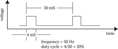
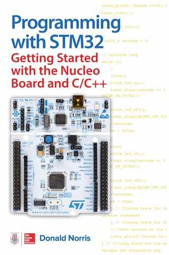
Figure 10-1 Typical PWM signal.
The first thing to note is that the signal is repetitive with a frequency around 50 Hz or an equivalent 20 ms period. This frequency is very common in servo control and it will be what I will use for the chapter projects. However, there is nothing limiting about this frequency and you can use any value up to the limit of what the MCU can support.
The second important feature is the duty cycle, which is a percentage of the amount of time the signal is in a high state to the total period, which is the sum of the high and low times. Duty cycle is often considered the primary property for a PWM signal, for it solely determines the servo position and LED luminescence.
It turns out that each type of device being controlled by PWM acts differently with the signal. I will describe each specific interaction when I go through the device demonstration.
General-Purpose Timer PWM Signal Generation
PWM signals are generated only by using either an advanced or a general purpose (GP) timer. This section describes the process on how this is done.
The signal generation is relatively simple and involves using a timer in an upcounting mode. The top portion of Figure 10-2 shows a timer counting up from 0 to a maximum 16-bit count equal to 65535.
Figure 10-2 PWM signal generation.
Each GP timer has a series of registers known as compare capture registers (CCRx), which store a number. When the upcounting reaches that number, an event is generated that depends on the timer mode. If the timer is set for a direct output as is the case for this PWM mode, then the event will be to turn on the channel associated with the CCRx register. In Figure 10-2, channel 1 is switched high when the count reaches 52428. The channel remains high until the timer counter reaches the maximum count (MAX) and overflows or resets as shown in the top waveform. The net result of this action is that a repetitive pulse is emitted from the channel 1 line with a 20% duty cycle. The following equation relates the timer count with the duty cycle (DC):
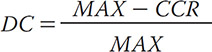
This equation may be rearranged to find the CCRx value given a desired duty cycle:
![]()
In Figure 10-2, I have also shown an additional channel output with a desired 60% duty cycle but no specific count shown for the CCRx register. I will use the second form of the equation to solve for T2, which is the count value to be stored in register CCR2:
![]()
Therefore, storing a value of 26214 in CCR2 will cause a 60% duty cycle pulse train to be generated from TIM2’s channel 2 output. Please note that the numbers I used for this calculation are relative in the sense that the actual CCRx numbers stored depend upon the real timer clock rate. You will shortly see that the numbers are much smaller, but the principle to figure them out is the same.
The TIM2 GP timer I used for PWM generation has a maximum of four output channels, meaning that it is possible to simultaneously generate four synchronized PWM signals using a single GP timer. One of the following demonstrations uses three channels, which is ample to demonstrate this capability.
Timer Hardware Architecture
Figure 10-3 is a portion of the GP timer block diagram highlighting the multi-channel outputs and associated CCRx registers.
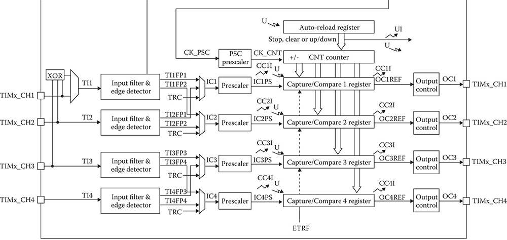
Figure 10-3 GP timer block diagram with four output channels.
The architecture is very straightforward, showing that each CCRx register has an input from the common timer counter (CNT) register as well as its own prescaled clock-rate input. This arrangement enables a very flexible PWM pulse train output to be implemented.
It is now time to describe how the HAL software enables PWM signal generation.
PWM Signals with HAL
The HAL framework uses a C struct named TIM_MasterConfigTypeDef to configure the timer peripheral generating a PWM signal. Each member will separately be discussed after the struct definition.
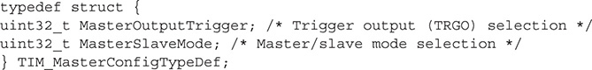
The TIM_MasterConfigTypeDef struct members are briefly defined in the following list:
uint32_t MasterOutputTrigger;—This value specifies the behavior of the trigger output (TRGO). This parameter can be any value of the following defines:
uint32_t MasterSlaveMode;—This is used to enable/disable the master/slave mode of a timer. This parameter can be one of the two values of the following defines:
![]()
A PWM timer configured using the TIM_MasterConfigTypeDef struct must further be initialized using the TIM_OC_InitTypeDef C struct, which is defined as follows:
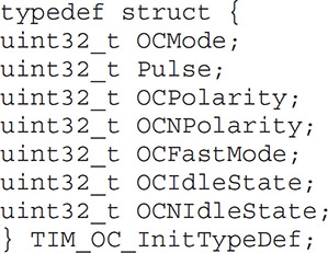
The TIM_OC_InitTypeDef struct members are briefly defined in the following list:
uint32_t OCMode;—Specifies the output compare mode. This parameter can be any value of the following defines:
TIM_OCMODE_TIMING—The comparison between the output compare register (CCRx) and the timer counter (CNT) has no effect on the output, which is known as a frozen mode.
TIM_OCMODE_ACTIVE—Set the channel output to active level on CCRx match.
TIM_OCMODE_INACTIVE—Set channel output to inactive level on CCRx match.
TIM_OCMODE_TOGGLE—Toggle channel output when the timer counter (CNT) matches the CCRx.
![]()
TIM_OCMODE_FORCED_ACTIVE—Force channel output high independently from the timer counter (CNT) value.
TIM_OCMODE_FORCED_INACTIVE—Force channel output low independently from the timer counter (CNT) value.
NOTE PWM Mode 1: When the timer is upcounting, the channel will be active for as long as the Period is less than the Pulse, otherwise it is inactive. In a downcounting mode, the channel is inactive for as long as the Period is greater than the Pulse, otherwise it is active.
PWM Mode 2: When the timer is upcounting, the channel will be inactive as long as the Period is less than the Pulse, otherwise it is active. In downcounting mode, the channel is active for as long as the Period is greater than the Pulse, otherwise it is inactive.
uint32_t Pulse;—This value be stored inside the CCRx register and it establishes when the output is triggered.
uint32_t OCPolarity;—Define the output channel polarity when the CCRx registers matches with the CNT. This parameter can be one of the two values of the following defines:
![]()
uint32_t OCNPolarity;—Define the complementary output polarity. It is a mode available only in TIM1 and TIM8 advanced timers, which allow two additional dedicated channels to generate complementary signals, i.e., when the channel 1 is HIGH then channel 1N is LOW and vice versa. This feature is especially useful for motor control applications. This parameter can be one of the two values of the following defines:
![]()
uint32_t OCFastMode;—Specifies the fast mode state. This parameter is valid only in PWM1 and PWM2 mode. This parameter can be one of the two values of the following defines:
![]()
uint32_t OCIdleState;—Specifies the state of the channel output compare pin during the timer idle state. This parameter can be one of the two values of the following defines:
![]()
NOTE This parameter is available only in TIM1 and TIM8 advanced timers.
uint32_t OCNIdleState;—Specifies the state of the complimentary channel output compare pin during the timer idle state. This parameter can be one of the two values of the following defines:
![]()
NOTE This parameter is available only in TIM1 and TIM8 advanced timers.
Enabling the PWM Function
You now need to enable the PWM alternative function in order to have the pulse width modulation function. The timer TIM2 is initially configured when creating the new project and having the Pinout window displayed. Figure 10-4 shows how TIM2 peripheral with PWM functionality is enabled in the Pinout view by selecting PWM direct output for channel 1 in TIM2. The PA1 pin is the channel 1 output.
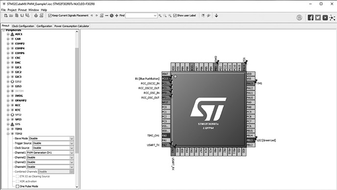
Figure 10-4 Enabling timer TIM2 with PWM output on channel 1.
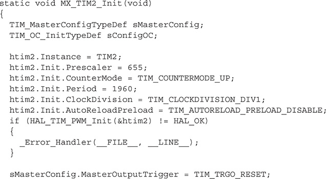
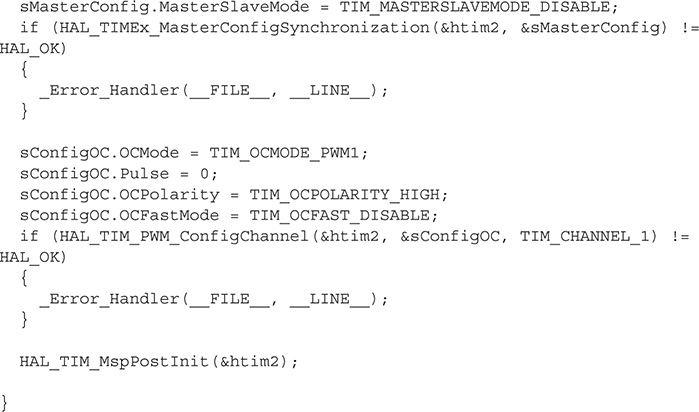
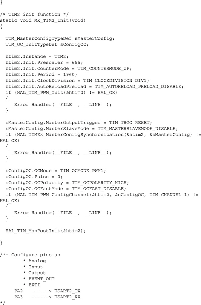
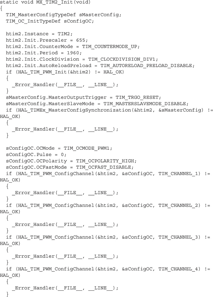
The CubeMX application will automatically insert an initialization method static void MX_TIM2_Init(void) in the main.c file when the TIM2 PWM function is enabled. Some additional parameters should also be set in the TIM2 object using the CubeMX Configuration tab, as shown in Figure 10-5.
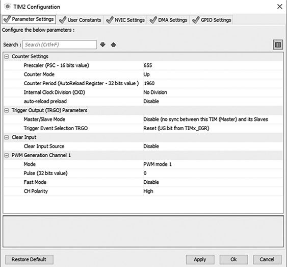
Figure 10-5 Configuration menu settings.
All of the initial PWM parameters are automatically set for you in the C code based upon the parameters you set in the TIM2 PWM IP tree view and the Configuration menu as shown in the following code snippet:
PWM Demonstration Software
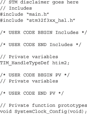
The newly generated main.c file now has a method that configures and initializes the TIM2 internal peripheral with a PWM output on its channel 1. There is no functional code running within the forever loop. The PWM signal generation is all done automatically in the background. This code is shown in the following code listing:
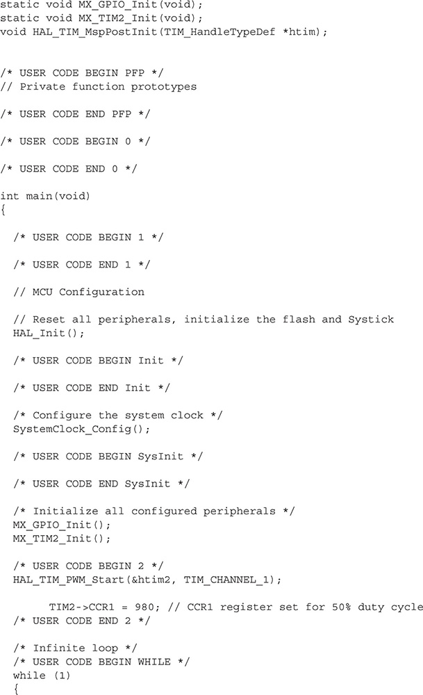
You should note that I set the prescaler to a 655 value. This meant that the TIM2 clock input would be at a frequency approximately equal to 977 kHz with a period of 10.23 µs. This value ensured that the timer resolution would allow for setting very precise pulse widths.
Demonstration One
This demonstration uses the values set during the initial configuration to generate a 50% duty cycle waveform. The program was first built and then downloaded into the project board. I used a USB oscilloscope to observe the PWM signal generated from the TIM2, channel 1 output, which is emitted from pin PA1. Figure 10-6 shows this waveform.
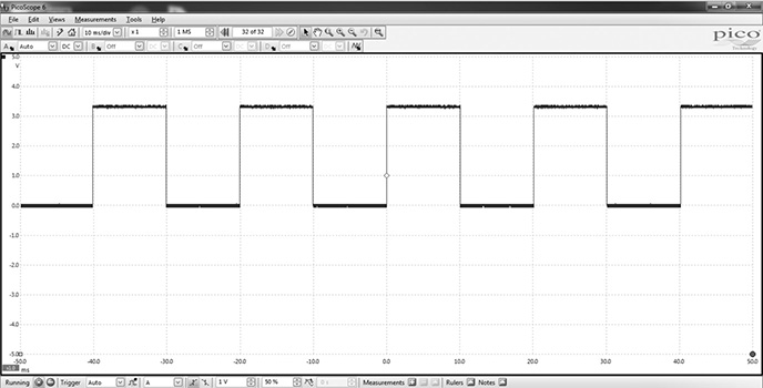
Figure 10-6 Fifty percent duty-cycle PWM waveform.
You should be able to see that the period of the over signal is 20 ms and the high time for the pulse is 10 ms, which creates the 50% duty cycle as expected. This waveform used a prescaler value equal to 655, which caused each timer count to be 10.23 µs as discussed above. The Period value was set at 1960, which means the actual period time is 1960 times 10.23 µs or 20050.8 µs, equivalent to 20.0508 ms. That was close enough for my purposes. The CCR1 register held a value of 980, which meant the output switched at 980 times 10.23 µs or 10025.4 µs, equivalent to 10.0254 ms. This is extremely close to a 50% duty cycle for all practical purposes. This demonstration proved that the PWM generation was working as desired.
Table 10-1 is provided as a handy reference showing a series of CCRx values that will generate a respective duty cycle given that value. Note that the small duty cycles shown at the table’s beginning are important for the servo control demonstration. This table is based upon a 50 Hz or 20 ms period PWM signal.
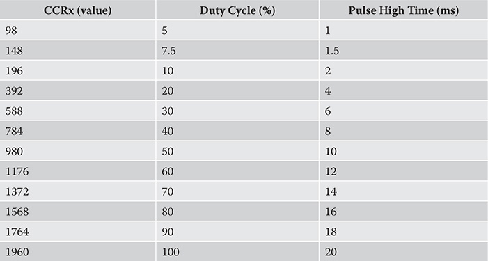
Table 10-1 CCRx Values and Corresponding Duty Cycles and Pulse High Times
Demonstration Two
This demonstration controls the intensity or luminescence of a single, red LED, using a PWM output as shown in the previous demonstration. The only parameter to be varied is the CCRx value assigned in the main method by this statement:
![]()
I chose to vary this value by editing the main.c file and then quickly rebuilding it. This process was very fast and not cumbersome at all. You could also set up an OpenOCD session and adjust the value in a dynamic fashion, but I found the edit, build, and download process to be very convenient without the bother of creating a telnet session. I would suggest you try both approaches and use whichever you find useful and productive.
Connecting Channel 1 PWM Output to an LED/Resistor
Figure 10-7 shows the connections for the same LED/resistor combination, which I earlier used for the project demonstration in Chapter 5. The LED/resistor is connected between PA1 and ground using the Arduino protoboard.
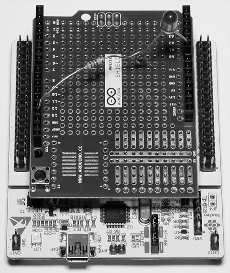
Figure 10-7 LED/resistor connected on the Arduino protoboard.
Test Results
I observed that the LED luminescence did vary considerably with the duty cycle of the applied PWM signal. You should realize one important distinction between dimming an incandescent bulb and an LED. The incandescent bulb intensity corresponds to the average voltage applied to it, while the LED luminescence depends on your eye’s integrative response. By this, I mean the voltage applied to the LED is at a constant level, but the time interval applied varies with the duty cycle. The human eye will tend to integrate or average out the LED light intensity and thus perceive different intensities for varying duty cycles. The eye also has a nonlinear relationship between actual luminance and perceived brightness, as shown in Figure 10-8.
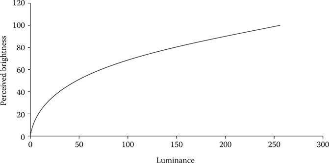
Figure 10-8 Human eye brightness perception.
What this all means is that the eye will more easily recognize different LED luminescence at small duty cycles but will not perceive any significant differences as the duty cycle increases. There are equations that model the eye brightness to luminance relationship quite well and have been codified as the CIE1931 lightness formula. White light LED manufacturers have modified their products using this relationship to make their commercial LEDs have a linear dimming property. I have not done this with this single LED demonstration, but it is quite doable and you would put the code into the main.c forever loop.
I did try to capture the intensity difference between 100% and 10% duty cycles. Figure 10-9 is a composite photograph with the 100% PWM on the left and the 10% PWM on the right.
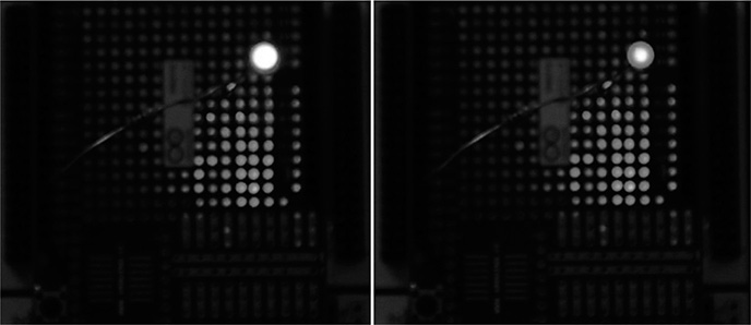
Figure 10-9 100% and 10% PWM signal-duty cycles applied to a red LED.
The camera shutter speed that was required for these images was fairly long, which tended to make the 10% image much brighter than it actually was. I guess you will just have to duplicate this demonstration and see the actual duty cycle versus perceived luminance for yourself.
Demonstration Three
In this demonstration I will be controlling a RGB LED that has three input lines, one for each color. GP timer TIM2 will be reconfigured to have three PWM outputs connected to each of the LED’s lines. The PWM lines will control both the LED color and luminescence based on the duty cycle set on each line.
The first step is to create a new CubeMX project to handle the additional PWM lines. Figure 10-10 shows the Pinout view where I have configured TIM2 for four channel outputs, of which I will use the first three to control the RGB LED.
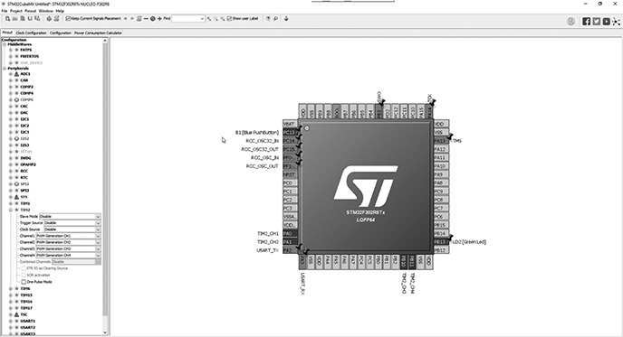
Figure 10-10 Enabling timer TIM2 with PWM output on channels 1 to 4.
The configuration menu is exactly the same as previously shown in Figure 10-5.
Connecting Channel PWM Outputs to a RGB LED
Figure 10-11 is a schematic showing the connections between the RGB LED and the timer GPIO pins as connected on the Arduino protoboard. Note that each LED line has a series current limiting resistor to protect both the GPIO pin and the RGB LED.
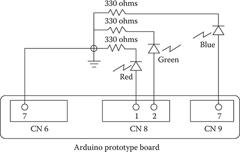
Figure 10-11 RGB to Arduino protoboard connection schematic.
The timer TIM2 channel outputs are on the following pins:
• Channel 1—PA0
• Channel 2—PA1
• Channel 3—PB10
• Channel 4—PB11
Figure 10-12 shows the physical setup for a RGB LED connected to an Arduino protoboard.
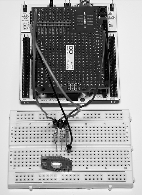
Figure 10-12 Physical RGB LED connections to an Arduino protoboard.
Software Modifications
A modified MX_TIM2_Init method will be added to the main.c file based on the additional channel outputs. This new method is listed below:
![]()
There is also some new code that must be entered into the main method. This new code is listed below:
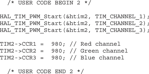
Note that each of the RGB channels was initialized at a 50% duty cycle.
Test Results
The RGB LED initially showed a bright white light, which was expected because all the individual LED components had the same duty cycle. I then reset the individual CCRx registers to separately test each color and confirmed that they were operating properly. I also tried varying the duty cycles to create different colors with little success because of the way the RGB LED was constructed. It did not merge the light from each colored LED and therefore did not properly create an alternate color, which you can do if you were mixing paint. I believe I would have been successful if I had used a more expensive RGB LED with some built-in optics, but unfortunately all I had was a very inexpensive RGB LED. In any case, the objective for this demonstration was to show you how to create and use multiple PWM outputs, which I believe was achieved.
Demonstration Four
This last demonstration will focus on using a single PWM signal to control a hobby-grade servo motor. I will be using the same program that was used for the first two demonstrations and no code modifications are required. I will start the demonstration by reviewing some basic facts regarding how analog servos are controlled.
Analog Servo Control
An analog servo is essentially an electric motor that has a built-in electronic circuit that converts specific pulse widths into a proportional rotation. The specifications for hobby-grade analog servos are fairly “relaxed” meaning that there are loose tolerances relating pulse width to physical rotation. This is mainly due to the use of very low cost components in both the electrical and mechanical components that comprise the servo. Table 10-2 details pulse width and expected rotation.
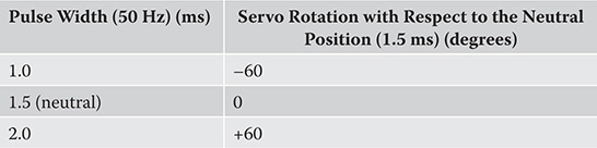
Table 10-2 Pulse Width and Servo Rotation
An analog servo should not move from its neutral position when it is sent a repetitive 1.5-ms pulse signal. A 1.0-ms pulse train will cause it to rotate its main shaft counter-clockwise 60°if viewed from head-on. Similarly, a 2.0-ms pulse train will cause it to rotate clockwise 60°. However, loose tolerances come into play and often the degree of rotation can be 10° to 15°, more or less.
In all cases, the pulse train frequency is set at a nominal 50 Hz or 20 ms period.
Figure 10-13 shows the hobby-grade servo I used for this demonstration. It is a Hitec model HS-311, which is a reliable, well-built servo.
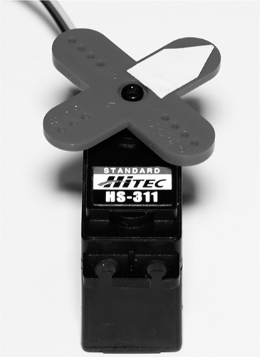
Figure 10-13 Hitec model HS-311 analog servo.
This servo takes quite a bit of current to operate, somewhat in excess of what the STM project board can provide. Consequently, I used a separate supply for it as may be seen in the Figure 10-14 connection schematic.
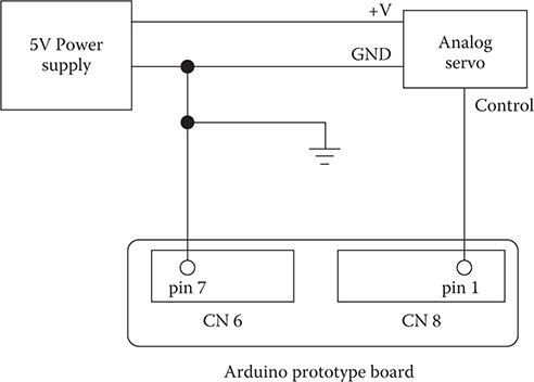
Figure 10-14 Servo connection schematic.
The servo control signal from the PWM output only requires several milliamperes, which is well within the GPIO pin drive capabilities.
Figure 10-15 shows the waveform for the 1.5-ms neutral position signal. It is a nice, clean signal with sharp rise and fall times, which are important for proper servo control.
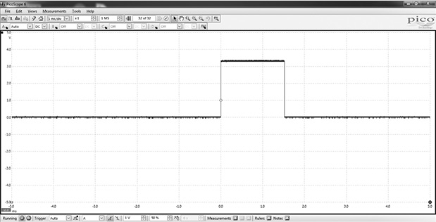
Figure 10-15 1.5-ms servo control signal.
The 1.0-ms and 2.0-ms waveforms are very similar except for the pulse width.
Figure 10-16 shows the physical setup with the analog servo connected to a solderless breadboard, which in turn is connected to the Arduino protoboard with jumper wires.
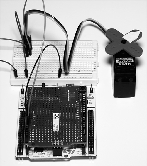
Figure 10-16 Servo test setup.
Test Results
I first changed the CCR1 value to 148, which causes a 1.5-ms pulse width to be generated. The servo immediately moved to its neutral position after the program was downloaded into the project board. I repeated the previous step with a CCR1 equal to 98, which generates a 1.0-ms pulse width. The servo responded by moving its main shaft 60° counter-clockwise. Finally, I changed CCR1 to 196, which generates a 2.0-ms pulse width. The servo’s main shaft rotated clockwise 120° as expected.
The servo performed flawlessly and showed no signs of jitter or vibration, which sometimes occurs with using hobby-grade servos.
I next added some functional code and placed it in the forever loop to continuously exercise the servo, thus eliminating the need to edit, rebuild, and download the controlling program.
Adding Functional Test Code
The following C code was placed within the main.c file in order to continuously control the servo. This code caused the servo main shaft to slowly oscillate between the ±60° end points.
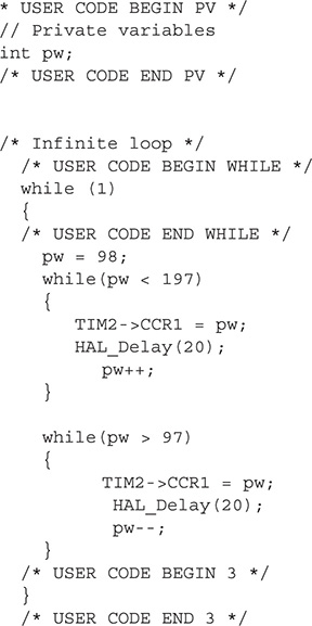
Test Results
I observed the servo main shaft to slowly oscillate between the end points as expected after the modified code was downloaded into the project board.
This final demonstration concludes the chapter. I believe I have provided you with a sufficient background that will enable you to successfully use servos with a STM Nucleo board.
Summary
I started this chapter on pulse width modulation (PWM) by explaining what makes up a PWM signal and detailing certain key properties of that signal. This was followed by a brief discussion of how the STM timer hardware generates a PWM signal.
Next came a discussion on how the HAL framework is used to both configure and initialize a general purpose (GP) timer to emit a PWM signal.
A complete C code listing was shown that generated a PWM signal with a 50% duty cycle and a 50-Hz output frequency.
Next followed the first of four PWM demonstrations. The first PWM demonstration just output the 50% duty cycle waveform that was generated by the project board after the code was built and downloaded into the board.
The second demonstration used a varying duty-cycle waveform to dim and brighten a red LED.
The third demonstration used multi-channel PWM waveforms to control both the color and intensity of a RGB LED.
The fourth and final demonstration illustrated how to control a standard analog servo using PWM signals.