5
General-Purpose Input Output (GPIO) and the STM Hardware Abstraction Layer (HAL)
As the formidable title states, this chapter deals with how GPIO operates on a STM Nucleo-64 board and how the HAL software is involved. It is important to first study the STM MCU architecture in order to fully understand how the GPIO ports function and their relationship to HAL. I would also acknowledge that many of the figures and table content are sourced from either the STM32F302R8 datasheet or reference manual. I would highly recommend that you download and have them readily available to help fill in any gaps in my discussions.
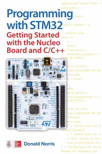
Figure 5-1 is the STM32F302R8 block diagram, which is the MCU used in the Nucleo-64 development board used in this book.
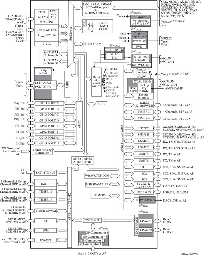
Figure 5-1 STM32F302R8 block diagram.
Note that there are six banks of GPIO ports shown on the left side of Figure 5-1, which are connected to the bidirectional advanced high-speed bus 1 (AHB1). This bus transfers digital data internally at a rate up to a maximum of 100 Mbps. HAL effectively manages the data transfers from the GPIO ports as well as from the many other peripheral components depicted in the figure.
I will start the HAL discussion by examining perhaps the simplest HAL module, which is the HAL_GPIO. This module has already been used multiple times in programs discussed in earlier chapters. The HAL_GPIO module was used without explanation simply because it was necessary to implement a required function such as blinking an LED or reading the state of a push-button switch. I will shortly closely examine the HAL_GPIO module, but first I will discuss the concept of memory-mapped peripherals.
Memory-Mapped Peripherals
STM MCU peripherals are controlled and data is transferred using addresses within a 32-bit range. This is known as memory mapping because it makes no difference from a programming perspective whether it is communicating with a memory location or a peripheral register. The 32-bit address range is usually represented by eight integer digits, meaning the total possible range of locations is 0x0000 0000 to 0xFFFF FFFF. Note that the hex number is preceded by a 0x and a space is paced after four of the leading hex digits. The 0x is a common programming construct indicating that the number is in a hex format and the space between the two hex number groups is just to make the number more readable. This address format is also used throughout the STM documentation.
Figure 5-2 shows the major blocks that constitute the entire 32-bit address range.
Figure 5-2 Complete 32-bit STM address range.
Also shown in Figure 5-2 are two breakout blocks, which detail the core memory locations as well as the peripheral/bus locations. I will next briefly discuss the core memory locations, which are important in their own right, but not very relevant to the peripheral address locations.
Core Memory Addresses
Table 5-1 shows the types of memory and their preassigned memory addresses.
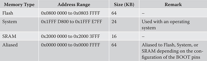
Table 5-1 STM Core Memory Address Ranges
One question that many readers might be pondering is how a PC can handle 8, 16, or even 32 GB of SRAM with only 32 bits of addressing capability? The answer lies in using both an operating system designed for extended memory accesses and a hardware unit known as a memory management unit (MMU). All the major PC OSs such as Windows, OSX, and Linux have extended memory functionality built-in that allows for 32-bit addressing to extend into multiple blocks or pages. You could think of using a 4-bit register, where each bit would activate a particular block or page. Therefore, bit 0 would allow access to all the base addresses starting at 0x0000 0000, while bit 1 would allow addressing to virtually start at 0x0001 0000 0000. Of course, there are only 32 real bits being used, but the OS handles the addresses as if they started one location beyond 0xFFFF FFFF. This 4-bit register can be thought of as being part of the MMU. Four bits means that a maximum of 64 GB can be handled in a 32-bit PC, which coincidentally is often the maximum SRAM that may be installed in such a PC. Of course, all practical physical memory limitations are relieved when a 64-bit system is used, but that requires an expensive CPU and additional energy requirements.
The preceding discussion is not applicable to a typical STM MCU because memory is quite constrained and vast amounts are not needed to handle typical embedded applications. I do want to mention that STM32F302R8 does incorporate a memory protection unit (MPU). The MPU is not a MMU, but is provided to manage CPU memory accesses such that one task will not accidentally corrupt or conflict with another task’s memory accesses. Memory can be arranged in up to eight areas with each area sized between 32 B and 4 GB, the last comprising the whole addressable memory range. The MPU is normally controlled by a real-time operating system (RTOS), which has an API contained within the CMSIS, which has been introduced in the last chapter. I will not be using the MPU for any of the book projects. You should consider its use only for the most safety-critical or mission-essential applications. Think of it being used in automotive or flight safety systems.
Peripheral Memory Addresses
Figure 5-3 shows the beginning portion of the memory addresses allocated to the STM32F302R8 peripherals,
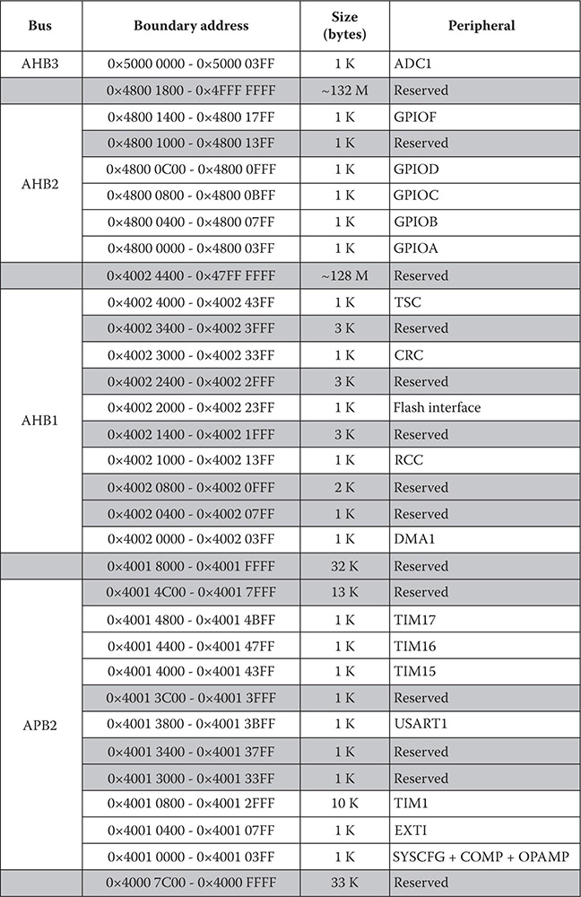
Figure 5-3 Beginning portion of the STM32F302R8 peripheral allocations.
You should be able to see that the AHB2 bus has the address range 0x4800 0000 to 0x4FFF 17FF. What is specific to this chapter’s focus is the total GPIO range of 0x4002 0000 to 0x4002 0x1FFF, which is divided into six smaller 1-KB blocks. Five of the six 1-KB blocks are allocated to GPIO ports A, B, C, D, and F, respectively. There is an unused block at range 0x4800 1000 to 0x4800 13FF, which has no significant impact on the port allocations. I have no idea why there is a reserved block allocated in what was a contiguous block allocation or why the final GPIO port is labeled F instead of E, as one might expect from the prior port designations. The port memory designation and allocation question probably can only be answered by the STM MCU chip designers. It is up to MCU users to accept the designations and allocations as they are and work with them to the best of their abilities.
I elected to include the following figure on peripheral locations for completeness sake and to provide a readily available reference for additional peripherals. Figure 5-4 shows the peripherals connected to the internal advanced peripheral bus 1 (APB1). The peripherals connected to the bus are as follows:
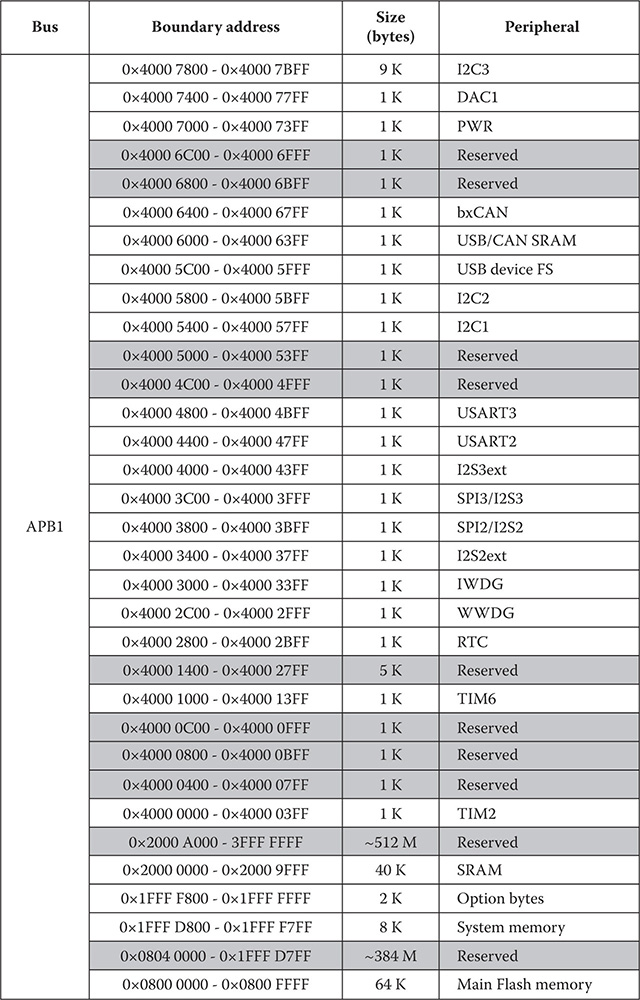
Figure 5-4 AHB1 peripheral allocations.
• Timers (TIMxx)
• Universal Synchronous/Asynchronous Receiver/Transmitters (USARTx)
• Serial peripheral interfaces (SPIx)
• Inter-integrated interfaces (I2Cx)
• Universal serial bus (USB)
• Integrated sound interface (I2S)
• Digital-to-analog converter (DAC)
• Controller area network interface (CAN)
• Real-time clock (RTC)
• Watch dog timers (IWDG, WWDG)
I will now return to the HAL_GPIO discussion after introducing to the concept of peripheral memory-mapped addresses.
HAL_GPIO Module
It would be wise to examine a sample GPIO circuit before discussing how it functions with the module software. It is always an important step to understanding the underlying hardware that implements the software.
GPIO Pin Hardware
Figure 5-5 is a block diagram, which also contains schematics that model a typical STM GPIO port pin.
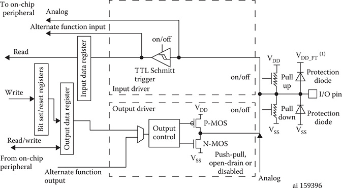
Figure 5-5 Typical STM GPIO port pin block diagram/schematic.
Starting from the right-hand side of Figure 5-5 you can see the I/O pin, which has robust overvoltage protection circuits attached. The GPIO pin is protected up to an applied 5-V input level in spite of the fact that the main MCU voltage supply is 3.3 V and the core processor voltages are 1.8 V. This makes interfacing quite easy without the need to employ voltage level shifters or resistance voltage dividers. The I/O pin is simultaneously connected to both input and output drivers as shown in the figure. However, only one driver at a time can be activated. Inspecting the input driver section reveals three possible inputs that may be sent to the core MCU. These are as follows:
• Analog: Bypasses the Schmitt trigger
• Alternate function: Schmitt trigger output
• Read: Output from one of the associated read register lines
The GPIO pin configuration settings determine which input is used at a given time.
Likewise, the output section has multiple ways of creating a signal output for the I/O pin. These are as follows:
• Write: Output from an associated write register line. The output register also has a R/W control line.
• Alternate function: Generated from an internal MCU peripheral.
Note that the output control block has two MOSFET transistors connected to the output control circuitry, which provide for the following operations:
• Push-pull
• Open-drain
• Disabled
Finally, the I/O pin has programmable enabled resistors attached to the pin, which will allow for the following:
• Pull-up
• Pull-down
• Neither
This sample circuitry is replicated for every GPIO pin existing in the MCU.
Each GPIO port has several registers attached to it, which control all of its pins’ behaviors by setting or resetting bits associated with the respective pins. Figure 5-6 shows the format for the GPIO port mode register for ports A … E and H.
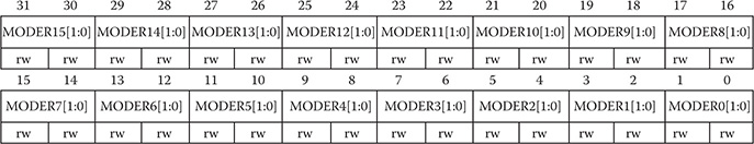
Figure 5-6 GPIO port mode register.
This register would be programmatically accessed by using the symbol GPIOx_MODER where x = A … E and H for the targeted port. The power-on reset values automatically placed in all the GPIO registers are as follows:
• 0x0C00 0000 for port A
• 0x0000 0280 for port B
• 0x0000 0000 for all other ports
The di-bit or two bit values that can be stored in a register have the following meanings:
• 00—Input mode
• 01—Output mode
• 10—Alternate function mode
• 11—Analog mode
Additional GPIO registers further configure other behaviors that are associated with the port pins including the following:
• Enabling push-pull, open-drain, or none (also called floating)
• Enabling pull-up, pull-down, or none
• Operational speed
The next two figures concisely display all the registers involved in all GPIO configurations. These figures are very important and will serve as the basis for configuring GPIO ports for all future projects. I had to break the GPIO register’s listings into two separate figures due to the number of involved registers. Figure 5-7 shows the first nine registers in order of their offset addresses to the base MODER address.
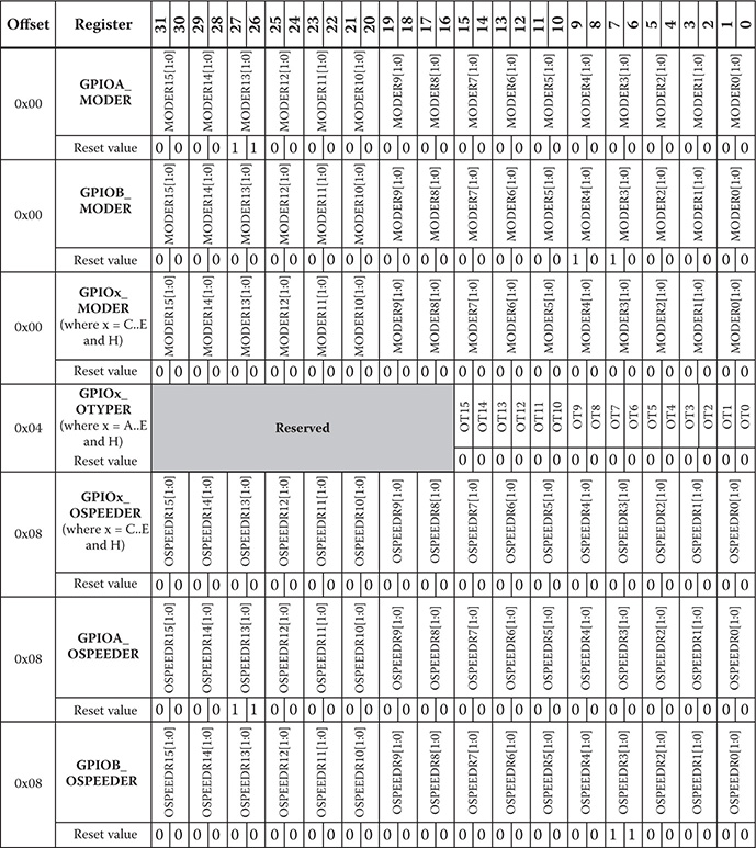
Figure 5-7 First nine GPIO registers’ details in order of offset addresses.
The last nine registers in the offset address order are shown in Figure 5-8.
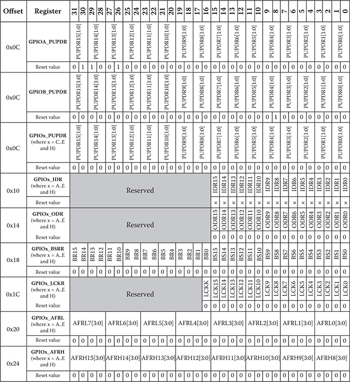
Figure 5-8 Last nine GPIO registers’ details in order of offset addresses.
The key to reading these figures is to understand what each register is supposed to control, its offset address, and how individual GPIO pins are accessed in the register.
I will next demonstrate a simple program that will control an LED attached to port A, pin PA10.
LED Test Demonstration
The purpose of the following demonstration is to show how to configure the port A GPIO registers to directly control an LED. The demonstration program will not blink the LED and you have to change the source code, recompile, and reload to affect the LED state.
However, there is a bit of hardware preparation that must be done before the test program can be run. That involves connecting the LED with a current limiting resistor to the selected port A pin. To ease this requirement, I elected to use an Arduino prototyping board, which is shown in Figure 5-9. This board is quite inexpensive and is readily available from a number of online sources.
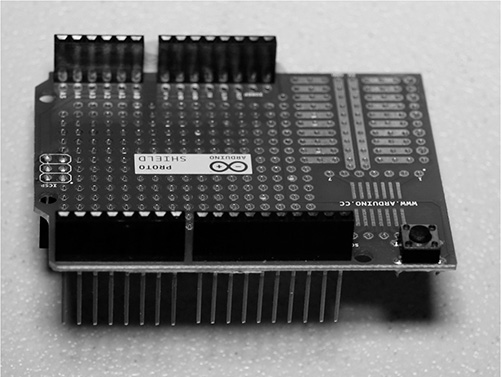
Figure 5-9 Arduino prototype board.
You will also need an LED and a 330-Ω 1/4-watt resistor to limit the current flowing through the LED. It will also be important to know which GPIO pins are exposed in the Arduino protoboard. This is easily answered by referring to the STM Nucleo-64 board user manual. Figure 5-10 comes from that manual and shows the STM32F302R8 pins associated with both the Arduino and Morpho connectors. In our case, only the Arduino pins are needed.
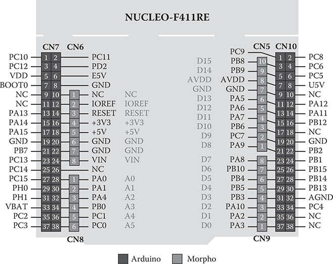
Figure 5-10 Arduino/Morpho pin connectors.
I arbitrarily selected PA10 as the LED output, simply because it was not already configured to a peripheral in the main.c template program. Figure 5-11 is the schematic used for this setup.
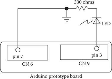
Figure 5-11 LED test schematic.
The longest LED lead is connected to the anode and the shortest lead is connected to the cathode. I simply soldered the resistor and the LED together because this arrangement allowed me to easily connect the LED/resistor combination to the protoboard, as shown in Figure 5-12. The protoboard is also plugged into the Nucleo-64 board for this photograph.
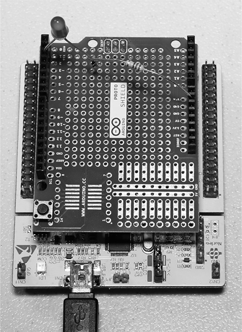
Figure 5-12 LED/resistor combination plugged into the protoboard.
It is time to work on the software once the hardware is all set.
LED Test Program
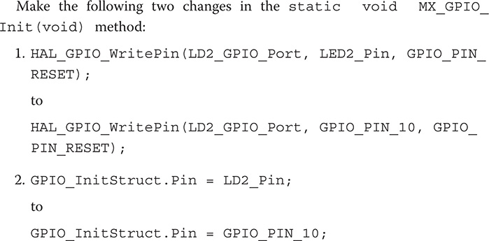
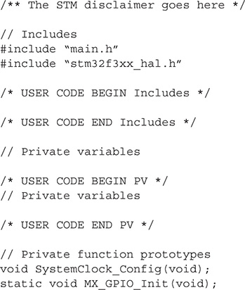
As I have previously mentioned, all STM peripherals, including GPIO ports are controlled by configuring a series of related registers, as detailed in Figures 5-7 and 5-8. In this demonstration program I will be configuring pin PA10, which is in the Port A GPIO bank of pins. PA10 will need to be configured as an output. I will be using a slightly modified main method created in the previous chapter’s project. You should set up a new project with this main method and simply modify the method by entering the following two lines and making two changes to the MX_GPIO_Init(void) method as detailed below.
Enter these two statements immediately after the first MX_GPIO_Init(} statement:

The HAL library relies on C structure named GPIO_InitStruct to configure any GPIO pin. Using this structure hides the necessity to use actual memory-mapped addresses to configure a GPIO pin. The following code segment from the MX_GPIO_Init(void) method shows how the structure is initialized to configure PA10 to an output pin:
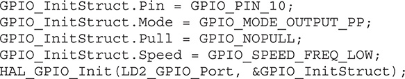
The last list statement is not part of the structure initialization but is required to apply the newly initialized structure within the HAL framework. The structure components are directly related to the memory-mapped GPIO registers, as shown in Table 5-2.
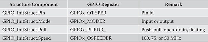
Table 5-2 GPIO_InitStruct to GPIO Register Equivalence
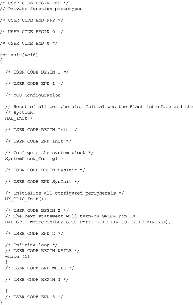
You should notice that the main method code listing ends with a while (1) statement, which simply forces the MCU to loop forever after the LED is turned on. The only way to turn off the LED is to disconnect the power to the board. Resetting the board will only immediately turn on the LED.
Test Run
You will first need to compile the project in preparation for uploading into the Nucleo-64 board. You then use the ST-LINK utility to transfer the hex file from the project’s Debug directory into the Nucleo, as previously described in Chapter 4. The LED should immediately turn on once the hex file is loaded into the board. Recheck the main.c code if the LED fails to turn-on. Incidentally, recheck that you have inserted the hardware into the proper pin sockets. Sometimes, it is as simple as that to fix a problem.
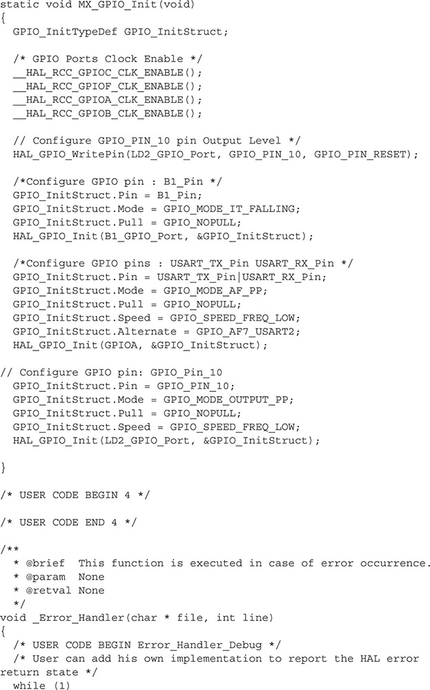
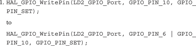
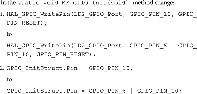
Enabling Multiple Outputs
It is relatively easy to modify the main.c file to enable multiple outputs. I selected GPIO PA6 as an additional output to control an LED. Incidentally, I referred to the defines contained in the main.h file to determine the pins already committed in the project. I have included the relevant portion of the file in the following listing for your use. Note that PA10 was not added as a define; I would have added that if I were building a permanent program instead of a transient demonstration program. The same is true for pin PA6.

Make the following changes to enable the multiple LED outputs.
In the main method change:
You will need to recompile and upload the new hex file into the Nucleo-64 board to test the new functionality.
Test Run
I left the LED/resistor combination connected between PA10 and ground to recheck that it turned on when the program was loaded. It is always wise to do that type of check because it sometimes happens that unintended things happen when a program modification is done, which is believed to not affect an existing and tested function. I next disconnected the LED/resistor circuit and reconnected it to PA6 and ground and confirmed that it also turned on the LED.
It would be straightforward to enable even more outputs using the same procedure. Just note that you would need to enable another GPIO port bank if you were to use all of the available pins in the GPIOA port.
Push-Button Test Demonstration
This demonstration will show you how to enable a GPIO pin input to detect when a user presses the blue user push button. An LED will light for as long as the push button is pressed. There is no additional hardware required for this demonstration other than what was needed for the previous LED demonstration. I will also be using GPIOA PA10 as an output pin to control the LED.
The MX_GPIO_Init(void) method has already configured the blue user push button, so all that is needed is to read the button state in the main() method. This is accomplished using the following statement:
HAL_GPIO_ReadPin(GPIOC, GPIO_PIN_13)
You should also recall from the Chapter 4 discussion that the blue user push button is connected to GPIO Port C, pin 13 and it is also constantly being pulled high. This means the button state will be high when not pushed and transition to a low value when pushed. The corresponding C snippet must continuously respond to this event as follows:
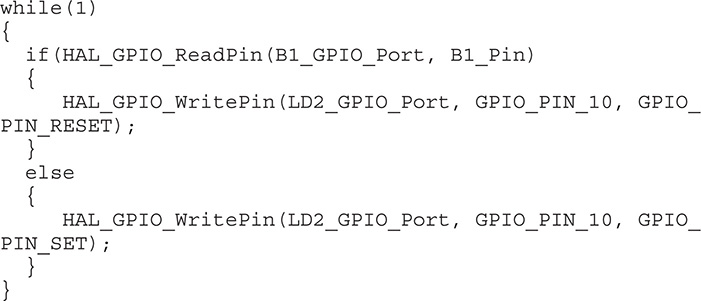
Enter the above code segment in the main() method to continue with the demonstration. Next compile and upload the hex file to the Nucleo-64 board.
Test Run
I observed that the LED turned on for as long as the push button was depressed. Note that you will have to use a small screwdriver to press the button as it is hidden under the Arduino protoboard.
The next demonstration concerns a basic property involved with all MCU signal operations, including the GPIO pins.
Clock Speed Demonstration
Clock speed as related to MCU signal operations is a misnomer. You would ordinarily consider it to be a measure of the maximum number of signal transitions per second. However, it is really a measure of the clock skew or amount of time it takes to transition a signal from 10% to 90% of the maximum value. It also applies in the opposite direction or going from 90% to 10% of the maximum value. The former is known as leading edge delay and the latter is called trailing edge delay.
Clock skew is directly related to true clock speed because the leading and trailing edge delays ultimately determine the maximum possible number of signal transitions per second. I will still refer to clock skew as clock speed because that is how STM choose to label this important signal property.
The important question that one should ask is why should clock speed even be considered. The answer lies in extending both MCU and battery life. The physics behind improving clock speed dictates that it takes energy or power, in this case, to overcome the circuit capacitance effects that mainly determine clock speed. Small amounts of additional power are required to improve the circuit switching times. This implies an increase in current flow from the battery over time and consequently a shortened battery life. In addition, increased power dissipation will induce small amounts of additional heat stress in the MCU and also shorten its life. The aforementioned are the main reasons why clock speed should always be selected to be the lowest level but still support required functionality.
This demonstration will illustrate the actual clock speed timings that are associated with the maximum and minimum clock speed settings. There are four speed settings available with the HAL framework, which are as follows:
• Low
• Medium
• Fast
• Very Fast
I will be using both the Low and Very Fast settings and applying them to signal outputs from pins PC0 and PC1, respectively. No additional MCU hardware is required. However, you will need a fast multi-channel oscilloscope to replicate this demonstration. The oscilloscope should also have a minimum bandwidth rating of at least 100 MHz. I used a Picoscope USB oscilloscope, model 3406B, to capture the measurements. This test device functions with a PC to measure and display up to four independent channels.
Setting the Pin Clock Speeds
The PC0 and PC1 pin clock speeds are set by creating two more GPIO_InitStruct C data structures and placing them in the MX_GPIO_Init(void) method. In addition, there will be a small amount of code required in the main() method.
The two new GPIO_InitStruct C data structures are listed below:
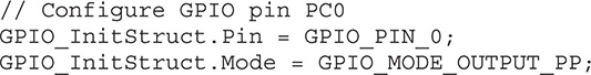
The new C structs set up the pins as identical GPIO outputs with the exception that one is low speed and the other is very fast speed. The code segment in main() simply toggles the pin outputs between high and low at the fastest possible rate because there is no other intervening code between the output statements.
Test Results
Figure 5-13 is a screenshot showing an instantaneous capture of the GPIO pin signal waveforms.
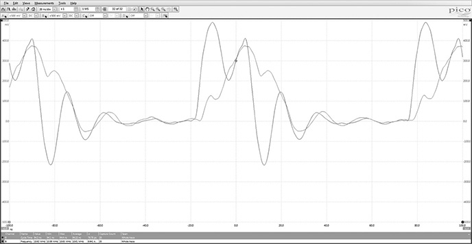
Figure 5-13 PC0 and PC1 pins’ signal waveforms.
It is easy to see that the signal waveforms are not crisp digital signals with sharp transitions but instead are slightly distorted with definite rising and falling edge slopes. The distortions are likely due to high oscilloscope probe capacitive loading and the slight inductance due to the jumper leads I connected between the oscilloscope probes and the Arduino protoboard sockets. I also used 10× high impedance probe settings to help reduce the loading on the GPIO pins. I know this helped because I repeated the measurements using the direct X1 probe settings, which further distorted the settings. The vertical voltage amplitude scale must be multiplied by 10 to account for the 10× probe settings.
If you carefully examine the figure you should see two automatic measurements that were computed by the oscilloscope on the displayed waveforms. I have repeated these measurements below for easy viewing:
Pulse period: 94.1 ns
Frequency: 10.62 MHz
I also closely examined waveforms in Figure 5-13 to estimate parameters that I used to calculate the equivalent bandwidth necessary reflecting the measured waveforms leading edges. I also used a rule of thumb for estimating the equivalent bandwidth using the leading edge rise time. These calculations follow:
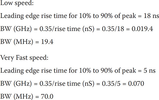
The 70-MHz bandwidth calculated for the Very Fast speed setting reflects several factors including the maximum possible AHB1 bus speed, which is 100 MHz and the STM32F302R8 high-speed clock rate, which is 72 MHz for the Nucleo-64 development board it controls. All-in-all, a 70-MHz bandwidth is fairly decent while the 19.4 MHz for the Low speed setting could be problematic for demanding applications such as very high-speed data communications. My experimental results actually agree quite closely with STM’s estimates of 75 MHz for the Very Fast setting and 25 MHz for the Low setting.
Summary
This chapter’s focus was on how to work with GPIO pins and the HAL. I began with a review of how STM peripherals are memory-mapped because that is the fundamental basis on how the MCU configures and controls them.
I next proceeded to discuss how a typical GPIO hardware pin is set up and the various functions by which it may be configured including as an input, an output, an analog role, or an alternate function. The various control registers associated with a GPIO pin were also discussed.
A simple LED test demonstration was next shown where I used an LED/resistor combination, which was inserted into Arduino protoboard sockets. The protoboard in turn was inserted into the Nucleo-64 development board. I went through all the program changes required to be entered into a main.c file in order to light the LED. A complete and annotated main.c listing was provided for your reference and use.
The above program was next modified to accommodate multiple outputs, which controlled an additional LED.
The next demonstration illustrated how the blue user bush button located on the Nucleo-64 development board could be programmed with a GPIO input pin to light an LED when it was pressed. The purpose of this program was to show you how to set up a GPIO pin as an input.
The last demonstration concerned how the GPIO clock speed parameter affected GPIO signal output waveforms. I explained that the clock speed was a misnomer and the real intent was to control GPIO signal skew. Skew is the time it takes to transition from one state to another state.