11
Direct Memory Access (DMA) and the Digital-to-Analog Converter (DAC)
This chapter content is carefully chosen to explain direct memory access (DMA) and the very useful digital-to-analog converter (DAC) peripheral, which takes advantage of efficient DMA data transfers. There are also several demonstration projects shown in the chapter, which show both DMA and DAC operations. The last one shows how to use DMA with the DAC peripheral
DMA
Data is normally transferred by using instructions executed by the Cortex-M core processor. This data is normally sent to or from internal memories and peripherals. This data transfer process consumes valuable processor cycles that could otherwise be put to use within a constrained embedded system. This is the reason why the DMA controller was designed. It can assume the data transfer process in many cases and allow the core processor to take on other critical embedded system processes.
Technically, the DMA controller can be considered a peripheral device; however, I prefer to think of it as more like a co-processor than a peripheral. Unlike any other peripheral, the DMA controller can take on the role of being a bus master, which is not allowed for any other device other than the core processor itself. In fact, thinking of the DMA controller as more of a bus controller is a good way to view this device.
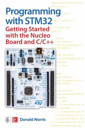
Figure 11-1 is a block diagram for the DMA controller used in the project board’s STM32F302R8 MCU. This figure will be very useful in explaining how the DMA controller works.
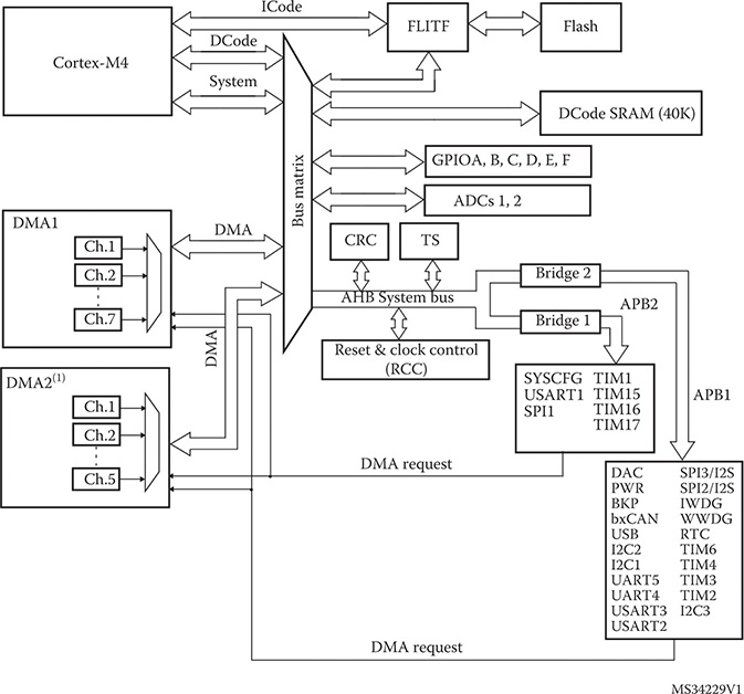
Figure 11-1 DMA block diagram.
NOTE DMA2, SPI1, TIM3, TIM4, UART4, UART5, and ADC2 are not available in the STM32F302R8 MCU.
It would be worthwhile to consider some of the basics of data transfers before going into the specifics of DMA operations.
Basic Data Transfer Concepts
Figure 11-2 is a simplified system block diagram where all the DMA components have been removed from Figure 11-1. The purpose of this diagram is to focus on how data transfers happen between the core processor and all remaining system peripherals.
Figure 11-2 Data transfers between the core processor and system peripherals.
You should clearly see that all data transfers between the core Cortex-M processor and any peripheral or internal memory must go through either the Bus Matrix or FLITF blocks. There is simply no other way that data can reach the processor. Every data transfer requires some amount of processor cycles to complete. For example, the processor must handle all data sent by an external device connected to a UART peripheral where that data is to be designated to be stored in SRAM. It is important to realize that the processor does not modify or change the data in any way, but simply sends it along to the proper memory storage locations. This requirement for core processor involvement ties up precious cycles that otherwise could be utilized for more efficient operations. A somewhat analogous model is where data is represented by cars and the processor by a city. Cross-country drivers wanting to go to a distant location are forced to go through a city with all its traffic lights and congested streets. It would be much better for the drivers if a bypass highway were available, allowing them to avoid going through the city. The DMA controller plays the role of the bypass.
Returning to Figure 11-1, you should be able to see that DMA1 controller, in the case of the STM32F302R8 MCU, connects directly to the Bus Matrix. This controller, as I earlier mentioned, is set up to be a bus controller or master and thus is able to configure the Bus Matrix to directly connect data between peripherals and internal memory, memory to memory, or even to another peripheral. These configurations are naturally named as follows:
• Peripheral-to-memory transfers
• Memory-to-peripheral transfers
• Peripheral-to-peripheral transfers
• Memory-to-memory transfers
The Bus Matrix controls the access of both the core processor and the DMA controller to various data busses, memory, and peripherals. It implements this control with a Round Robin algorithm, which ensures equitable access to both controllers. Figure 11-3 is a block diagram illustrating how the Bus Matrix is connected with all the system components.
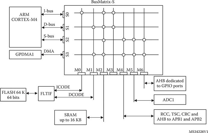
Figure 11-3 Bus Matrix block diagram.
The Bus Matrix is a complex circuit that interconnects the following master and slave devices:
• Core Cortex-M processor (master)
• DMA controller(s) (master)
• Flash memory interface (FLITF) using the ICODE (slave)
• Flash memory interface (FLITF) using the DCODE buss (slave)
• Direct connection to SRAM (slave)
• Advanced High-Speed Bus 1 (AHB1), which connects to the Advanced Peripheral Busses (AHB1 and AHP2) through bridge circuits (Bridge 1 and Bridge 2) (slave)
• Advanced Peripheral Bus (APB) connected to the GPIO pins (slave)
• Direct connection to the ADC1 peripheral (slave)
DMA Controller Details
Every STM32 DMA controller contains two master ports, one named the memory port, which connects to internal memory such as SRAM and flash. The other is named the peripheral port and it connects to the Advanced High-Performance Bus (AHB). The AHB in turn connects with the slave peripherals. In the STM32F302R8 DMA controller, the peripheral port can also connect to a memory control circuit permitting memory-to-memory transfers.
STM32 DMA controllers also have one slave port connected to the AHB bus. This allows the DMA controller to be programmed from the other master, that is, the core processor.
The STM32F302R8 DMA controller has seven independent and programmable channels, which are each connected to separate hardware lines. These are how the slave peripherals can request a response from the DMA controller. The exact nature and type of request is configured during the MCU hardware design phase. Different STM MCUs will have a varying numbers of channels as well as different request types depending upon the MCU design requirements.
There is also a priority assignment hardware unit, which allows different priorities to be assigned to the seven DMA request channels. Higher priorities will normally be assigned to fast peripherals needing immediate DMA response as well as to any memory accesses.
Figure 11-4 shows all seven DMA channels along with their respective peripheral request signals that are bound to them during the MCU design phase.
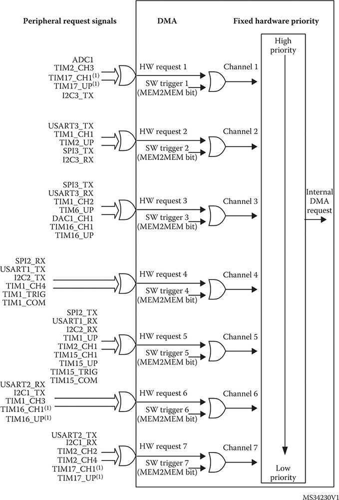
Figure 11-4 DMA channel block diagram.
Figure 11-4 is an important figure because it will be your ready reference to use when trying to determine which DMA channel to use for a given peripheral DMA request. It is very important to note that only one peripheral can be active on a given peripheral request line.
Notice in Figure 11-4 that the DMA channels have default priorities, which are fixed in hardware with channel 1 being the highest and progressing to channel 7 as the lowest. However, these default priorities may be overridden with user-assigned priorities, designed to determine which peripherals have preference when accessing the AHB. DMA channel lines are normally trigged through hardware signals from selected peripherals but they can also be activated by software. Software triggering is the means by which memory-to-memory transfers are activated.
Using HAL with DMA
The HAL framework uses a C struct named DMA_HandleTypeDef to configure the DMA controller. Each member will separately be discussed after the struct definition.
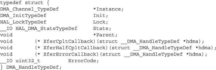
The DMA_HandleTypeDef struct members are briefly defined in the following list:
• DMA_Channel_TypeDef *Instance;—This is the pointer to the DMA/Channel pair descriptor which will be used. For example, DMA1_Channel5 indicates the fifth channel of DMA1. Recall that these designations are bound to peripherals during the MCU design. Refer to Figure 11-4 to see the channel-to-peripheral designations.
• DMA_InitTypeDef Init;—This is an instance of the C struct DMA_InitTypeDef, which is used to configure the DMA/Channel pair. This value will be further explained below.
• HAL_LockTypeDef Lock;—DMA locking object.
• __IO HAL_DMA_StateTypeDef State;—DMA transfer state.
• void *Parent;—This is a pointer used to keep track of the peripheral handlers associated with the current DMA/Channel. For example, if we are using a UART in DMA mode, this field will point to an instance of UART_HandleTypeDef.
• void (* XferCpltCallback)(struct __DMA_HandleTypeDef *hdma);—This is a pointer to a callback function, which is used to signal user code that a DMA transfer is completed. It is automatically called by the HAL when a DMA interrupt is paired, by the function HAL_DMA_IRQHandler().
• void (* XferHalfCpltCallback)(struct __DMA_HandleTypeDef *hdma);—This is a pointer to a callback function, which is used to signal user code that a DMA transfer is completed, half-completed, or an error occurred. It is automatically called by the HAL when a DMA interrupt is paired by the function HAL_DMA_IRQHandler().
• void (* XferErrorCallback)(struct __DMA_HandleTypeDef *hdma);—This is a pointer to a callback function, which is used to signal user code that a DMA transfer has an error. It is automatically called by the HAL when a DMA interrupt is paired by the function HAL_DMA_IRQHandler().
• __IO uint32_t ErrorCode;—DMA error code.
The HAL framework uses a C struct named DMA_InitTypeDef to initialize the DMA controller. Each member will separately be discussed after the struct definition.
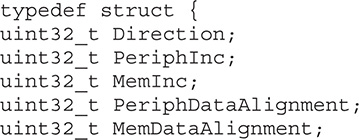
The DMA_InitTypeDef struct members are briefly defined in the following list:
• uint32_t Direction;—This value defines the DMA transfer direction. This parameter can be any value of the following defines:
• DMA_PERIPH_TO_MEMORY
• DMA_MEMORY_TO_PERIPH
• DMA_MEMORY_TO_MEMORY
• uint32_t PeriphInc;—This value can automatically increment the peripheral register holding the data address to be transferred. This parameter can be one of the two values of the following defines:
• DMA_PINC_ENABLE
• DMA_PINC_DISABLE
• uint32_t MemInc;—This value can automatically increment the memory port register holding the memory data address to be transferred. This parameter can be one of the two values of the following defines:
• DMA_MINC_ENABLE
• DMA_MINC_DISABLE
• uint32_t PeriphDataAlignment;—This value set the sizes of the peripheral data elements to be transferred. This parameter can be any value of the following defines:
• DMA_PDATAALIGN_BYTE
• DMA_PDATAALIGN_HALFWORD
• DMA_PDATAALIGN_WORD
• uint32_t MemDataAlignment;—This value set the sizes of the memory data elements to be transferred. This parameter can be any value of the following defines:
• DMA_MDATAALIGN_BYTE
• DMA_MDATAALIGN_HALFWORD
• DMA_MDATAALIGN_WORD
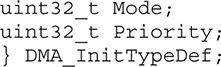
• uint32_t Mode;—This value sets the DMA mode. In the normal mode, the DMA controller sends the specified amount of data from the source port to the destination port and then stops. The controller must be rearmed for another transfer. In the circular mode, the DMA controller sends the content of the source data buffer, resets to the first byte in source data buffer, and starts sending the buffer again. In the transmission interim, the peripheral will have had a chance to refill the source buffer so there will be fresh data in the source buffer. In this case, the source buffer is also called a ring buffer. The DMA circular mode is also called the continuous mode for obvious reasons. This parameter can be one of the two values of the following defines:
• DMA_NORMAL
• DMA_CIRCULAR
• uint32_t Priority;—Use this value to assign a priority to a DMA channel. This parameter can be any value of the following defines:
• DMA_PRIORITY_LOW
• DMA_PRIORITY_MEDIUM
• DMA_PRIORITY_HIGH
• DMA_PRIORITY_VERY_HIGH
Final Steps in Setting Up a DMA Transfer
There are just a few more steps required in order to configure a DMA transfer over a selected channel. These are as follows:
1. Set up appropriate memory and/or peripheral port addresses
2. Establish the size of the data transfer
3. Arm the DMA controller
4. Enable the DMA mode on the selected peripheral
The HAL framework abstracts the first three steps with the following statement:

The fourth step is dependent on the selected peripheral. You will normally consult the STM data sheet, which describes the selected peripheral in order to determine how to enable the DMA transfer and to find out the exact channel it has been preassigned. Remember from the earlier discussion that peripherals have been preassigned channel numbers during the MCU design phase. In the following example, I will be demonstrating how to use USART2 peripheral in the DMA mode.
Demonstration One
This first demonstration will involve sending a string using the USART2 peripheral operating in the normal DMA mode. There are just a few steps necessary to configure this demonstration:
1. First configure the USART2 peripheral using the Pinout view in the CubeMX application as has been done several times in previous demonstrations.
2. Set the DMA1 channel as follows (STM32F302R8 MCU) for the USART2 peripheral for a memory-to-peripheral transfer:
a. USART2_TX = DMA1/CH7
b. USART2_RX = DMA1/CH6
The following statement sets the USART2 peripheral DMA1, channel 7 to output characters to a terminal program:
![]()
It must be put in the main method. In addition, there is no need to instantiate DMA1, channel 6 because no characters will be received from the terminal program in this demonstration.
3. Enable the USART2 peripheral for DMA operations and arm the appropriate channel to execute the transfer.
The following statement enables the USART2 peripheral for DMA operations:
![]()
It must be put in the main method.
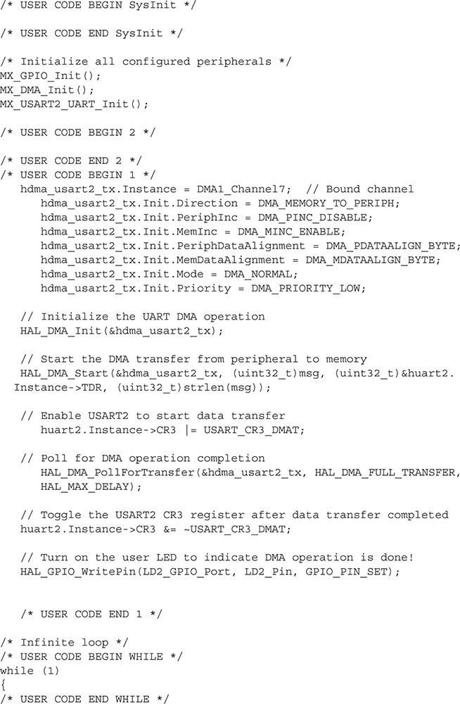
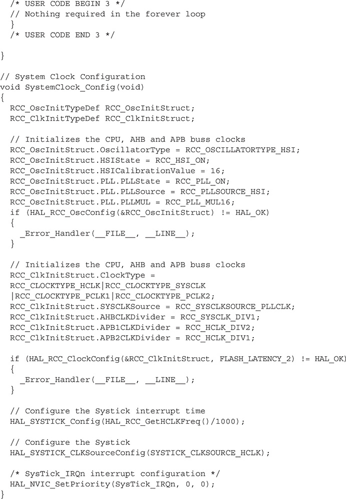
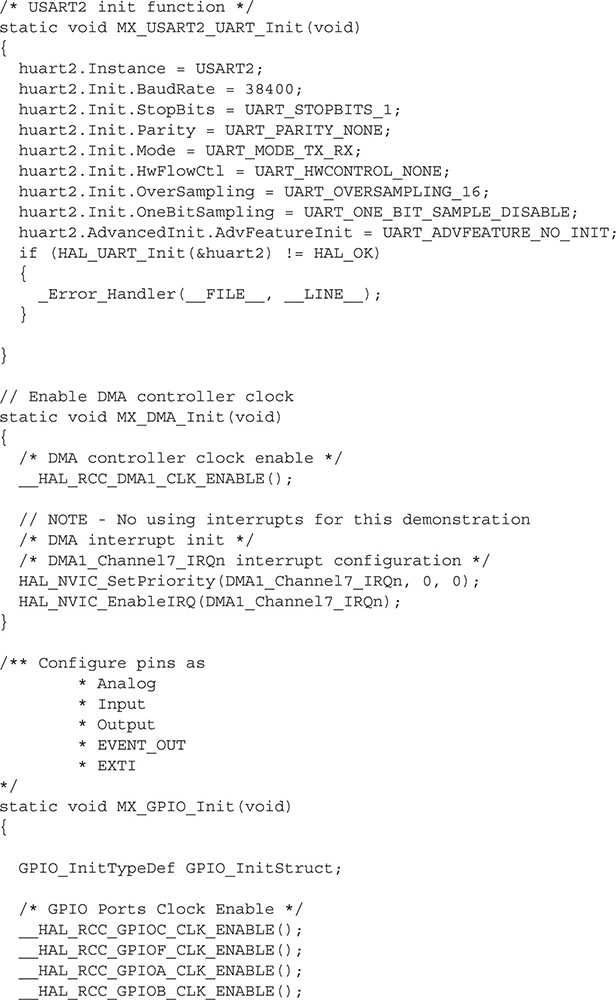
Program Listing
The following is the code listing for this demonstration. I have also provided some additional discussion regarding pertinent code segments following the listing.
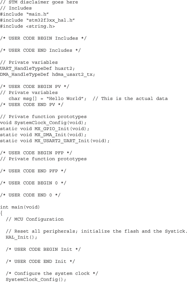
I have first configured and initialized all the appropriate DMA setting in the main method. Some DMA_InitTypeDef struct members were not set because they are not needed in this demonstration and their values are not read during this particular DMA operation. The first three steps in the DMA preoperation sequence are as follows:
1. Set up appropriate memory and/or peripheral port addresses.
2. Establish the size of the data transfer.
3. Arm the DMA controller.
These steps were all accomplished using the following statement:
![]()
The fourth and the final step is to start the DMA operation for the selected peripheral. This was accomplished by the following statement:
![]()
The seventh bit in the USART2 control register CR3 is named DMAT and is set to commence normal DMA operations for this peripheral.
The core processor has also been set up to poll to determine when the DMA operation has been completed. This operation was accomplished by the following statement:
![]()
Polling for completion is completely appropriate for this demonstration simply because it is a “one-shot” occurrence and does not impede, nor conflict with any other MCU operations.
Finally, the USART2 peripheral is disarmed from further DMA operations by using the following statement:
![]()
Test Results
I observed that the user LED did light after the hex file was downloaded into the project board. However, I desired a better indication that the DMA operation did run successfully. To do this, I started the Realterm application and monitored the virtual communications port that is logically connected to the USART2 peripheral. Figure 11-5 shows the screen capture displaying the data message sent out from the peripheral.
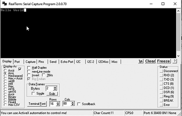
Figure 11-5 Realterm screen display.
This absolutely confirmed that the USART2 peripheral transmitted the data message to memory via DMA.
This demonstration should now have convinced you of the DMA usefulness. It is time to introduce the DAC peripheral and really demonstrate how DMA can significantly improve MCU operations.
DAC Peripheral
I will first explain the principles behind the DAC peripherals in order for you to understand how it requires rapid data transfers to operate efficiently.
DAC Principles
The DAC design used in STM MCUs is based on a R-2R resistor ladder network concept. This concept is easily explained by referring to Figure 11-6.
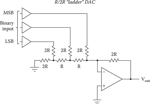
Figure 11-6 R-2R design concept.
The resistive network acts like a programmable voltage divider between a reference voltage and ground. The usual reference voltage (Vref) for the STM DAC is the main 3.3-V supply. There is a 3-bit DAC, shown Figure 11-6, which makes it easy to discuss. In reality the DAC used in the project board has a 12-bit input.
The binary inputs shown in Figure 11-6 are switched between 0 V and Vref or 3.3 V. If a bit is high, it will cause its voltage input to weighted in the summed voltage output according to its bit position.
The output voltage (Vout) for the 3 bit (N = 3) example for a given digit binary input (Value) is determined by the following equation:
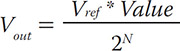
Therefore, if the maximum value equals 7 or in binary terms 111, the maximum Vout will be:
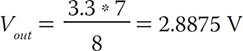
This result happens because the step size is 3.3/8 or 0.4125. This is a rather large error and only happens in this case due to the small number of bits involved. For the real 12-bit STM DAC, the step size would only be 3.3/4096 or 0.00080566 V or roughly 0.8 mV. That step size will provide an excellent analog voltage representation for a digital number. Returning to the digital example, I have calculated all eight analog voltage outputs for all the possible binary combinations. These are shown in Table 11-1.
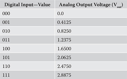
Table 11-1 Binary Input vs Analog Voltage Output—3-bit DAC Example
Figure 11-7 shows the analog voltage output in more start terms where it becomes very apparent that there is no smooth transition between binary input values due to the limited number of bits.
Figure 11-7 Bar chart showing analog voltage outputs.
Table 11-1 and Figure 11-7 provide more than ample proof that a sufficient number of bits must be present to have a somewhat smooth and continuous voltage output from a DAC. However, there will still be a small noise present even with a high number of bits present due to the inherent switching that is constantly happening with the DAC. This noise may be easily filtered out using an active low-pass analog filter. However, I will demonstrate that the DAC output is very clean and can be directly used as is without additional filtering.
A STM DAC also has the option of switching in a buffer output amplifier. This device will lower the DAC’s output impedance and provide additional drive current without the need to add an external output operational amplifier for this purpose.
It is now time to discuss the HAL software that can configure and initialize the STM DAC peripheral.
HAL Software for the DAC
The HAL framework uses a C struct named DAC_HandleTypeDef to configure the DAC peripheral. Each member will separately be discussed after the struct definition.
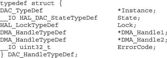
The DAC_HandleTypeDef struct members are briefly defined in the following list:
• DAC_TypeDef *Instance;—This is a pointer to the DAC descriptor which will be used. For example, DAC1 is the descriptor for the first DAC peripheral.
• __IO HAL_DAC_StateTypeDef State;—This value represents the DAC communication state.
• HAL_LockTypeDef Lock;—This value is a DAC-locking object.
• DMA_HandleTypeDef *DMA_Handle1;—This is a pointer to a DMA handler configured to perform digital-to-analog conversions in DMA mode.
• DMA_HandleTypeDef *DMA_Handle2;—This is a pointer to a DMA handler configured to perform digital-to-analog conversions in DMA mode.
• __IO uint32_t ErrorCode;—This is a value representing the DAC error code.
The DAC_HandleTypeDef struct differs from all the other similar structs in that it does not have an Init member, but instead relies on a different type of C struct to initialize the DAC at the channel level. This C sruct is named DAC_ChannelConfTypeDef and has the following definition. As before, each member will separately be discussed after the struct definition.
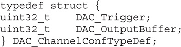
The DAC_ChannelConfTypeDef struct members are briefly defined in the following list:
• uint32_t DAC_Trigger;—This value specifies the source used to trigger the DAC conversion. This parameter can be any value of the following defines:
• DAC_TRIGGER_NONE—Used for a manual trigger.
• DAC_TRIGGER_SOFTWARE—Used when DAC is in a DMA mode without a timer.
• DAC_TRIGGER_Tx_TRGO—Used when DAC is driven by a dedicated timer.
• uint32_t DAC_OutputBuffer;—Specifies whether the DAC channel output buffer is enabled or disabled.
Demonstration Two
In this demonstration I will be manually triggering the DAC to output a repetitive voltage ramp.
Program Listing
The following is the code listing for this demonstration. I have also provided some additional discussions regarding pertinent code segments following the listing.
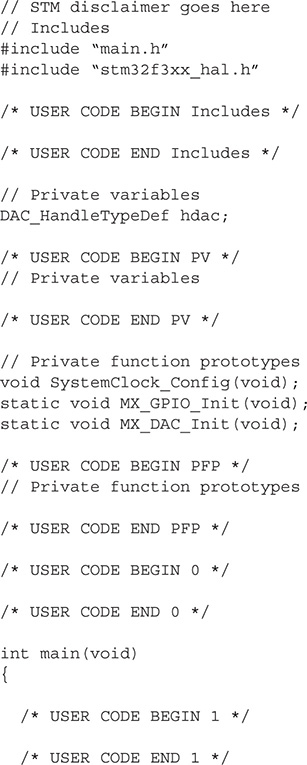
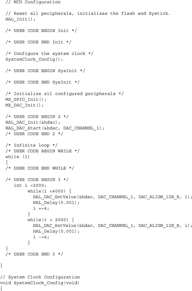
The significant addition to this basic code is the DAC Init function MX_DAC_Init. The CubeMX application generated this code when the DAC peripheral was enabled during the project creation process. There is really nothing remarkable that is happening in this function other than the output buffer is enabled and any DAC trigger is disabled.
The functional code that produces an output waveform is located in the forever loop of the main method. This code segment is relisted below to allow for an easier reference:
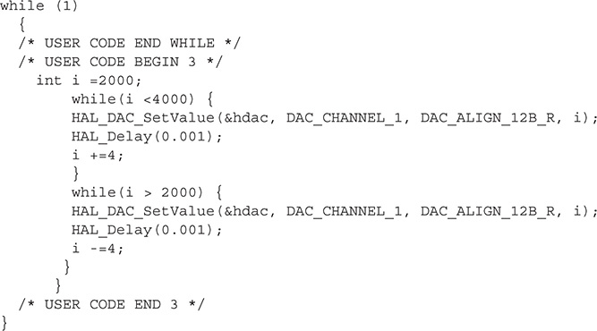
There are two while loops within the forever loop, one which counts up and outputs a slowly increasing voltage and other counts down and outputs a slowly decreasing voltage. The waveform period is determined by the delay value, which in this demonstration has been set to 1 ms between each digital incremental value. The HAL_DAC_SetValue method causes the DAC to output on DAC channel 1 an analog voltage based on the 12-bit, right endian justified value for the index i.
Test Results
Figure 11-8 is a screen shot from a USB oscilloscope connected to PA4, which is the DAC channel 1 output for the STM32F302R8 MCU.
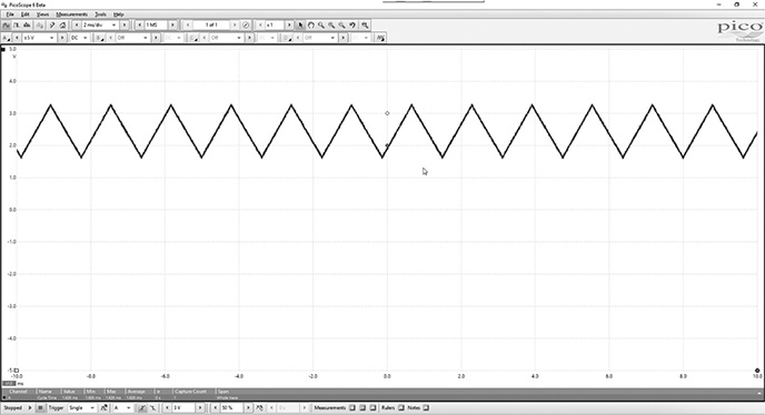
Figure 11-8 DAC output.
You can see that it is relatively clean triangular waveform with a 1.626-ms period or an approximate frequency equal to 615 Hz. The peak-to-peak amplitude varies between approximately 1.6 and 3.3 V. These particular voltages are a result of using the values 2000 and 4000 as the DAC input limits, respectively.
I am reasonably sure that you can also increase the waveform frequency by decreasing the delay in the code as described above. Readers should try experimenting to determine the ultimate frequency limit.
Demonstration Three
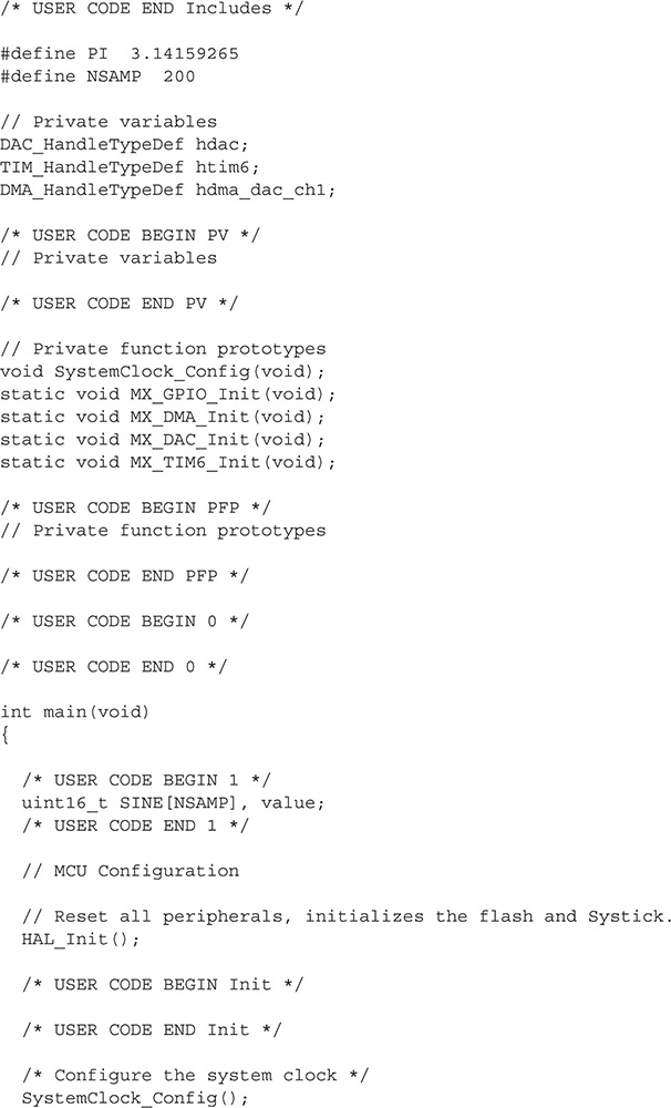
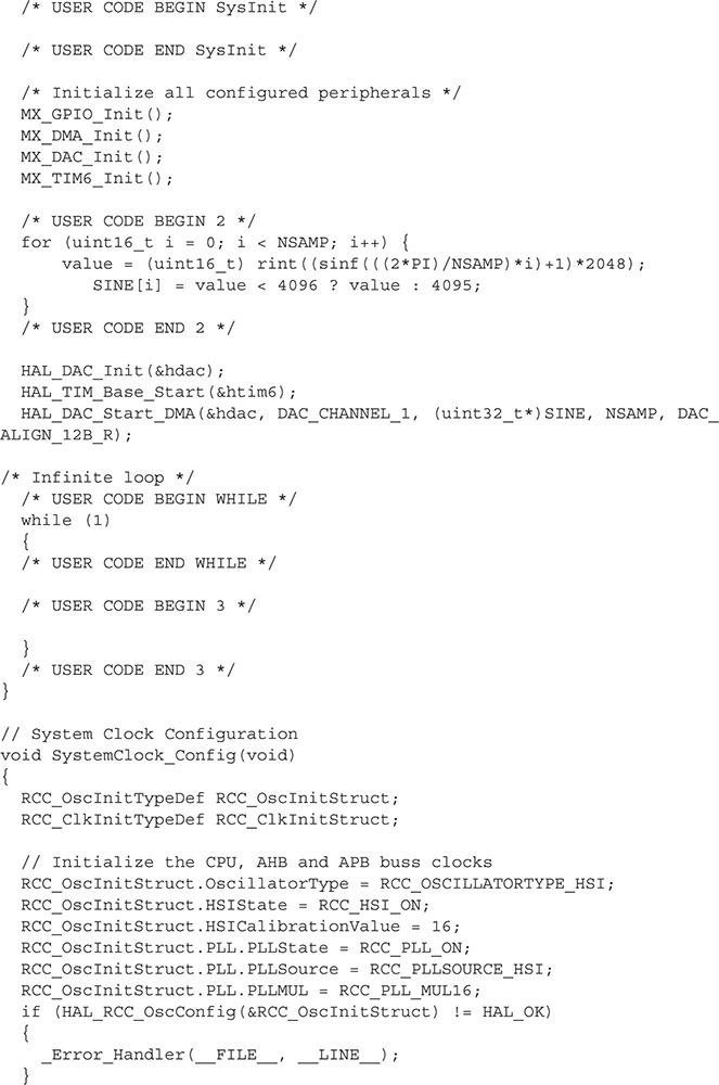
In this last demonstration I will be operating the DAC in a DMA mode to output a sine wave that is synthesized by the application. Generating an analog signal is a common task assigned to a DAC. DMA is the preferred operational method because it frees up the core processor to attend to higher priority tasks rather than focusing on generating binary input for the DAC. The following generalized statement both starts the DAC and performs a DMA data transfer from memory to the peripheral:

In this demonstration, only one DAC channel named DAC_CHANNEL_1 is available. The argument uint32_t* pData is a data pointer, which in this case will point to the beginning of the 200 element SINE array. The uint32_t Length argument is the number of data elements to be transferred, which is the NSAMP constant with value 200. Finally, the uint32_t Alignment argument specifies the data element bit size and whether the data is right or left justified. In this case, the define DAC_ALIGN_12B_R shows the data is 12-bit and is aligned to the right, meaning that the least significant data bit is also the rightmost bit.
Synthesizing a sine wave requires setting the number of increments or steps that will go into making up a single cycle waveform. In this example, the number was set at 200, which is a good trade-off between having a representative sample and minimizing the total steps that need to be constantly handled. The resulting equation used to synthesize a 12-bit sine wave is as follows:
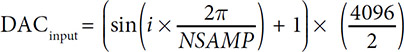
This equation was used to synthesize a single sine wave cycle with the i step ranging from 0 to 199.
I next arbitrarily selected a period of 15 ms for the DAC sine wave output or an equivalent frequency of 66.67 Hz. This means that the conversion rate must be set at 66.67 * 200 or 13,334.
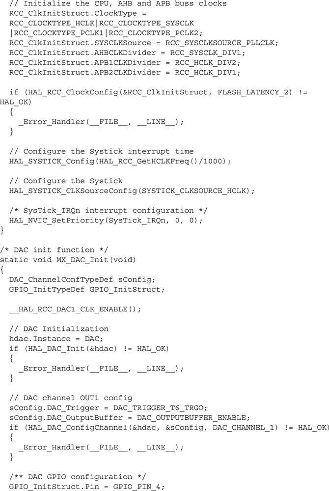
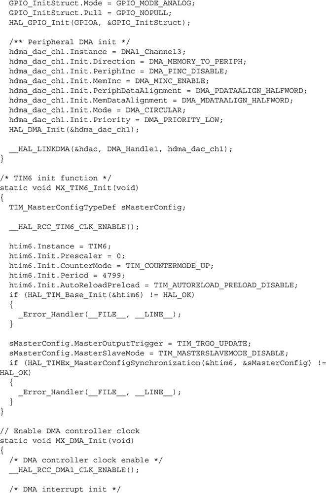
The timer TIM6 is used as trigger for the DAC’s TRGO line and its period must then be set to 13,334. The high-speed external clock (HSE) input into TIM6 was set at 64 MHz with no prescaling. This all means the timer period value must be set to 64 MHz/13.33 KHz or approximately 4800. The actual period value was set at 4799 to account for the added 1 that goes into to the timer frequency calculation.
Program Listing
The following is the code listing for this demonstration. I have also provided some additional discussions regarding pertinent code segments following the listing.
Test Results
Figure 11-9 is a screen shot from a USB oscilloscope connected to PA4, which is the DAC channel 1 output for the STM32F302R8 MCU.
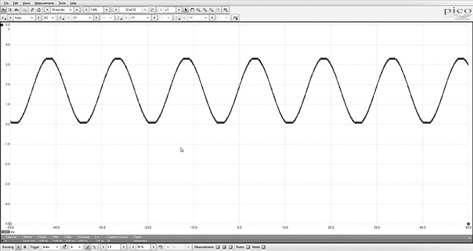
Figure 11-9 DAC output.
You can see that it is a relatively clean sine waveform with a 15-ms period or an approximate frequency equal to 66.67 Hz. The peak-to-peak amplitude varies between approximately 0 and 3.3 V. This waveform is exactly what was programmed.
Figure 11-10 is an averaged spectrum display, which shows the main frequency components in the DAC sine wave output signal.
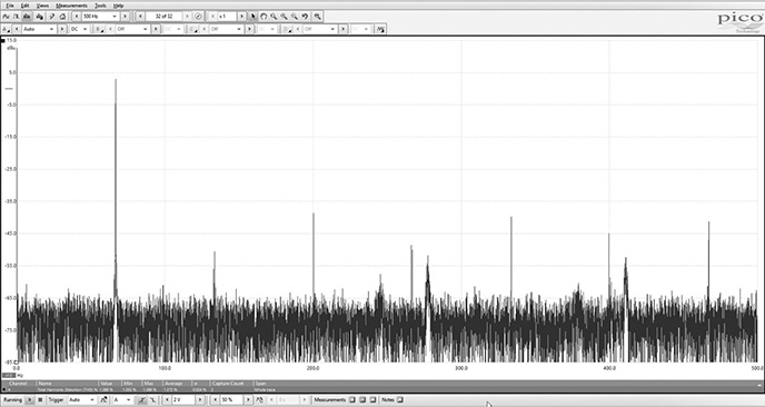
Figure 11-10 Sine wave spectrum display.
The average total harmonic distortion (THD) was measured at only 1.372%, which is very low for this type of signal generation. The third harmonic at 200 Hz was the highest distortion component and was measured at –42 dBu, which is less than one-hundredth of the primary frequency’s amplitude.
I also experimented by changing the timer TIM6 period to determine the highest possible output frequency. I determined that a minimum period value of 105 created a sine wave frequency slightly over 3 kHz. Any value lower than that period value simply caused the DAC to remain at steady high level.
The last point I will make, which is the same one that I have often repeated, is that the core Cortex-M processor is not involved with this signal generation once it has been configured, initialized, and started. Notice that the forever loop in the main method is completely devoid of any functional code because the signal generation is completely being accomplished by a combination of hardware and firmware. This approach is the essence of efficient and effective embedded design.
Summary
This is a combination chapter that explains both direct memory access (DMA) and the digital-to-analog converter (DAC). I chose this combination because the DAC is an ideal peripheral to use with DMA operations.
The first section explains the theory behind DMA and how a DMA controller effectively implements this operational mode.
The next discussion focuses on how to use the HAL framework to both configure and initialize the MCU for DMA operations. I presented a detailed discussion concerning two C structs that are critical for setting up the DMA mode.
The first demonstration simply has the USART2 peripheral sending a character string to memory using the DMA mode. A complete program listing was provided with all the important details concerning DMA operations highlighted.
The next section introduces the DAC and provides a brief background on how it functions. This is followed by a section on how to use the HAL framework to configure and initialize this peripheral.
The second demonstration illustrates how to have the DAC generate a triangular waveform using functional code placed in the main method’s forever loop. This demonstration was purposefully designed to be computationally “heavy” in anticipation of the next demonstration.
The third and final demonstration shows how the DAC could generate a relatively “pure” sine wave using a DMA mode and then being periodically triggered by a timer. The initial signal was set at a 66-Hz frequency, but I eventually was able to generate sine wave signals slightly exceeding 3 kHz. The signal waveforms were generated without any core processor involvement other than the initial configuration.