
Photovoltaic Energy Generation and Control for an Autonomous Shunt Active Power Filter |
|
CONTENTS
12.2 Consequences of Harmonic Pollution
12.3 Principle of Sliding Mode Control
12.3.1 Choice of Sliding Surface
12.3.2 Determination of the Reference Current
12.4 Characteristics of the System
12.4.1 The Electrical Equations
12.4.2 Projection in the Rotation Reference
12.4.4 Description of the Control Laws
12.4.5 Sliding Mode Existence Conditions
12.5.1 Solar Cell Model Using Orcad
12.5.2 Maximum Power Point Tracking
12.5.3 Direct Current Voltage Optimization with the Photovoltaic Source
12.5.4 Control of the Switching Frequency
The past several decades have seen a rapid increase of power electronics-based loads connected to the utility system [1]. However, the proliferation of these nonlinear loads has raised concern with regard to the effect of the resulting harmonic distortion levels of the supply current on the power system [2]. Passive filtering is the traditional method of harmonic filtering. However, it is well known that the application of passive filters creates new system resonances that are dependent on the specific system conditions. Although this solution is simple, it gives rise to several shortcomings. Furthermore, since the harmonics to be eliminated are of low order, large filter components are required [3]. The active power filter (APF) is an efficient solution to solve the problems created by nonlinear loads; the concept is shown in Figure 12.1. We will use it in this work.
Hybrid APFs (HAPFs) have been developed in which a passive filter is connected parallel to a conventional APF [4]. The HAPF configuration is effective in improving the damping performance of high-order harmonics. Our system consists of the following five parts:
1. Source: alternating current (ac) line sinusoidal, balanced or not
2. Photovoltaic (PV) array: a nine-module (85 W each) PV array with 1000 W/m2 insolation and a boost direct current-direct current (dc-dc) converter
3. Nonlinear load: a bridge diode rectifier feeding a resistive inductive load
4. Three-phase inverter
5. Resistor/inductor/capacitor (RLC) passive power filter
Recently, there has been increasing concern about environmental pollution. The need to generate pollution-free energy has triggered intensive efforts to find alternative sources of energy. Solar energy, in particular, is a promising option. Some researchers have worked on developing a combined APF and PV system [5,6]. However, existing HAPF configurations, with all their benefits, are not yet implemented for PV applications.

FIGURE 12.1 Circuit diagram of a shunt APF connected to a nonlinear load.
12.2 CONSEQUENCES OF HARMONIC POLLUTION
Many of the effects of harmonics on electrical equipment and installations can be cited [5]. The greatest effects are overheating and interference with networks.
• Heating: Total losses due to the joule effect are the sum of the losses due to the fundamentals and harmonics; it is defined by Equation 12.1:
(12.1) |
where Ih is the harmonic current, which represents the fundamental range for h = 1, and R is the resistance traversed by the current. Harmonics also increase iron and copper losses. They become more important in devices based on magnetic circuits (motors, transformers, etc.). In power electronic equipment, these harmonics can shift the voltage zero crossing and lead to malfunctioning of medical instruments and other electronic devices. Furthermore, losses and malfunctions caused by the presence of harmonic currents markedly reduce the performance of equipment such as motors, transformers, and so on.
• Aging of insulation: Insulation aging often results from tensile stress due to the presence of harmonics and thus a local increase in leakage current, or to excessive heating in the conductors. The most spectacular example of this type of effect is the destruction of equipment (condenser, breaker, etc.).
• Interference with telecommunication systems: The electromagnetic coupling between electric and telecommunication networks can cause interferences. The importance of the interference depends on the amplitude and the frequency of electric currents and the importance of electromagnetic coupling between the networks. For example, parts of the telecommunication networks may be rendered unusable in the case of resonance. The unintentional generation, propagation, and reception of the electromagnetic energy and the effect of these harmonics on the equipment items or systems must be analyzed and characterized. This is referred to as electromagnetic compatibility.
• Malfunctioning of electrical equipment: In the presence of harmonics, the voltage, the current, or both can change sign several times in a half period; therefore, sensitive equipment at the zero crossing of these electrical parameters is perturbed.
• Risk of resonance excitation: The instantaneous effects of resonance are due to capacities or inductances that can have resonant frequencies close to harmonic frequencies. This is the case when the batteries are connected to the network capacity to meet the power factor; resonance frequencies can be quite low, and thus coincide with those of the harmonics generated by static converters. In this case, there will be an amplification of harmonic phenomena; surges occur and damage the cables, transformers, protection systems, battery capacity, and so on.
Various quantities are defined to quantify this disturbance:
• The total harmonic distortion (THD) rate defined by:
(12.2) |
where Ih is the h-order harmonic component and I1 represents the fundamental component
• The overall harmonic distortion: we characterize the pollution of a whole network by the THD in the voltage or current as
(12.3) |
Generally, the harmonics included in electrical networks are lower than 2500 Hz. They correspond to harmonic terms from rank 2 to 50 and are considered low-frequency disturbances. The higher-frequency harmonics are greatly attenuated by the skin effect and the presence of the inductances of lines. In addition, the devices that generate harmonics mostly have an emission spectrum below 2500 Hz; this is why the harmonics study field generally extends from 100 to 2500 Hz, that is, from rank 2 to 50 [1].
• The power factor: For a signal wave, the power factor is given by the ratio between the active power and the apparent power S. Generators, transformers, transmission lines, and control devices influence the measurement of voltage and current ratings. A low value of the power factor often results from poor use of these facilities.
In the case of harmonics, an additional power called the deformans power is defined mostly when the power is produced by a nonsinusoidal source. The active power in periodic nonsinusoidal signals is defined by
(12.4) |
where Un and In are the root mean square values of the voltage and current harmonic of order n, and ϕn is the phase shift between them. The reactive power can then be defined by
(12.5) |
However, these definitions do not conform to the equation of the power triangle:
(12.6) |
The apparent power is defined by
(12.7) |
Then
S2=∑nU2n∑nI2n≥(∑UnIncosϕn)2+(∑nUnInsinϕn)2 |
(12.8) |
The quantity D is added using the following equation:
(12.9) |
We can write the apparent power as follows:
(12.10) |
The Fresnel diagram of the powers is shown in Figure 12.2.
Distorting power consists mainly of the cross-product of the voltage and current harmonics of different orders and will be reduced to zero if the harmonics are reduced to zero, that is, under sinusoidal conditions:
(12.11) |
If only the current is nonsinusoidal, then:
(12.12) |
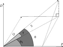
FIGURE 12.2 Fresnel diagram of the power deformans.
The major drawback of this definition is that it is not certain that the power factor is equal to unity if the reactive power (by definition) is reduced to zero and the reactive power can be fully compensated by inserting inductive or capacitive components.
• The power factor (F.P.) becomes:
(12.13) |
It is clear that the harmonics affect the power factor.
12.3 PRINCIPLE OF SLIDING MODE CONTROL
The sliding mode design approach is one of the effective nonlinear robust control laws. Sliding mode control has been widely applied to power converters due to its characteristics, such as speed, robustness, and stability to large load variations. It provides system dynamics with an invariance property to uncertainties once the system dynamics are controlled in the sliding mode. It consists of two components. The first involves the design of a switching function so that the sliding motion satisfies the design specifications. The second is concerned with the selection of a control law that will make the switching function attractive to the system state. It can be seen that this control law is not necessarily discontinuous. Let the nonlinear system be in the following form with a scalar control:
(12.14) |
where X is the system error and U is the control issued by the corrector with variable structure. The second member of the equation is discontinuous due to the discontinuity imposed on the control side of the surface σ(x) = 0. Depending on the order applied, the system will take one of the following two forms, as shown in Figure 12.3:
(12.15) |

FIGURE 12.3 System behaviors on the sliding surface.
(12.16) |
A nonlinear system is given by the differential equation:
(12.17) |
where X∈nℜ, U∈mℜf(X,t)∈nℜg(X,t)∈n×mℜ
How should the variable structure for the command be applied? Two questions can be asked:
1. What is this control?
2. How can it be synthesized?
The synthesis of a variable structure, represented by Figure 12.4, involves two phases [5]:
• The first is to define the switching surface σ(x)=0 of the desired dynamics.
• The second aims to synthesize the control function u(x, t), in order to make sure that [6] any state outside the switching surface will be joined to the states inside the sliding tranche (with bandwidth 2δ surrounding the sliding surface; see Figure 12.5) during a finite time (limited by the switching frequency of the insulated gate bipolar transistor). Once it reaches them, a sliding mode occurs. The system adopts the dynamic of the surface and the point representing the evolution of the system reaches the equilibrium point.

FIGURE 12.4 Schematic diagram of variable structure control.

FIGURE 12.5 Trajectories of sliding mode, ideal and real.
The dynamic slip is independent of the control, which only serves the evolution of the intersection of surfaces and ensures their attractiveness. From any initial condition, the representative point of the movement meets the hypersurface slip in a finite time.
12.3.1 CHOICE OF SLIDING SURFACE
Generally, the sliding surfaces are chosen as hyperplanes through the origin of space, and their control is shown in Figure 12.4.
The general shape of these surfaces is given by the following equations:
(12.18) |
(12.19) |
Although the surface may be nonlinear, the linear surfaces are more practical for the design of a corrective variable structure sliding mode in the case of a multivariable system. We consider the following nonlinear system:
(12.20) |
where X∈nℜ, U∈mℜf(X,t)∈nℜg(X,t)∈n×mℜ
The problem is more complex due to the existence of several switching surfaces (σ1, σ2, σ3, …, σm. The sliding mode occurs on the intersection of these surfaces.
The two switching surfaces are chosen as
(12.21) |
(12.22) |
(12.23) |
The switching surface σ(x) = 0 is a surface of dimension m, and σi(x) is the ith switching surface. The intersection of the surface σ(X) is a sliding surface dimension (n − m). Each entry has the form Ui:
U(X,t)={U+with σi(X)>0U−with σi(X)>0 i=1, …,m |
(12.24) |
The switching surface is chosen such that, when the system is in sliding mode, the behavior is meeting the desired objectives. After selection of the sliding surface, an important phase remains to be considered. Can we ensure the existence of a sliding mode? If the tangents to the trajectories or velocity vectors near the surface are directed toward the switching surface σ(x) = 0, then a sliding mode occurs on this plane.
Let us consider the canonical form:
{˙xi=xi+1 i=1, …,n−1˙xn=−n∑i=1aixi+f(t)+U |
(12.25) |
where U is the command with discontinuities in the vicinity of σ(x) = 0. It should be noted that the disturbance f(t) and the parameters may be unknown.
The switching surface is of the form:
(12.26) |
where the coefficients are constants. The following pair of inequalities constitutes the conditions to the existence of the sliding mode:
(12.27) |
To prove the invariability with respect to the coefficient ai and f(t), solve Equation 12.26 to equal 0, and substitute it into Equation 12.25.
Once the system is in sliding mode, the closed-loop system becomes
{˙xi=xi+1 i=1, …,n−2˙xn−1=−n−1∑i=1cixi |
(12.28) |
The system no longer depends on f(t) or on the ai coefficients; on the contrary, it depends on the parameters ci, which gives the system an invariance to disturbances and parametric variations.
Let the system be described by Equation 12.15, and a surface σ separate the hypersurface into two parts, G+ and G−:
(12.29) |
with X = [x1, …, xn]T; F = [f1, …, fn]T. The functions f1, …, f are piecewise continuous and have discontinuities on the hypersurface σ of equation σ(x) = 0.
f+N
The sliding condition can take two equivalent forms, given by Equations 12.30 through 12.32:
(12.30) |
(12.31) |
(12.32) |
where
(12.33) |
In the ideal sliding mode case, the switching frequency is assumed to be infinite. In practice, the frequency is limited by the power electronic components. As a consequence, some hysteresis effects are introduced. They increase the phenomenon of “chattering” embodied by the oscillations around the sliding surface, but do not call into question the theory of sliding. Figure 12.5 shows the effect of hysteresis bandwidth 2δ. The balance point can be arbitrarily chosen, but an origin allows faster convergence to the sliding surface. Commutations move freely within the bandwidth around the surface. An oscillating phenomenon appears around the equilibrium point. These trajectories are shown in Figure 12.5.
Consider the monovariable state system described by Equation 12.20; the equivalent control of the ideal sliding mode (neither threshold, nor delay, nor hysteresis) is obtained on σ(x, t) = 0 with ˙σ=(x,t)=0
⋅σ=(x,t)=(∂σ∂x)Tdxdt+∂σdt=(∂σ∂x)T[f(x,t)+g(x,t)Ueq]+∂σdt |
(12.34) |
Ueq(x,t)=−[(∂σ∂x)Tg(x,t)]−1{(∂σ∂x)Tf(x,t)+∂σ∂t} |
(12.35) |
The condition of the sliding mode is
(12.36) |
This condition is also called the transversality condition. In reality, the fact that the product is zero means that the vector field g is orthogonal to the surface normal vector. So g has no vertical component and system status cannot be brought to the surface. This condition is necessary but not sufficient to ensure the sliding mode.
By replacing the expression of the equivalent control in the system of Equation 12.20, we obtain the following expression:
˙x={I−g(x,t)[(∂σ∂x)Tg(x,t)]−1(∂σ∂x)T}f(x,t)−g(x,t)[(∂σ∂x)Tg(x,t)]−1(∂σ∂x)T |
(12.37) |
The equivalent control shown in Figure 12.6 maintains the system state on the sliding surface σ = 0. The average value that takes control is defined as follows
min{U−(x,t),U+(x,t)}〈ueq〈max{U−(x,t),U+(x,t)} |
(12.38) |
The necessary and sufficient condition for the sliding mode’s existence is given by
Umin=min{U−(x,t),U+(x,t)}Umax=max{U−(x,t),U+(x,t)} |
(12.39) |
12.3.2 DETERMINATION OF THE REFERENCE CURRENT
In an APF application, the dynamic performance of the sliding mode control will also depend on the algorithm used for identifying the current harmonics [7]. The method adopted to extract the reference currents and the synthesis of different regulators (control loops of voltage and current) will ensure a sinusoidal current on the network. Different methods of identifying the harmonic (or the fundamental) current components of a nonlinear load can be used. In the following study, we will present and analyze, respectively, the p-q method of instantaneous powers and the direct method. Their use will depend on the targets: harmonic compensation, its application to three-phase installations (under balanced or unbalanced conditions), or single-phase installations. The p-q technique is illustrated in Figure 12.7.

FIGURE 12.6 Representation of the equivalent control.

FIGURE 12.7 Overall system configuration and control block diagram.
In order to generate the compensation current that follows the reference current, a fixed-band hysteresis current control method is adopted. The proposed scheme is designed to inject the reactive and harmonic current of the nonlinear load and the reactive current of the passive filter. Furthermore, a current must be drawn from the utility source to maintain the voltage across the dc-bus capacitor to a preset value that is higher than the amplitude of the source voltage. Under normal operation, the PV system will provide active power to the load and the utility. Under poor PV power generation conditions, the utility source supplies the active power to the load directly.
12.4 CHARACTERISTICS OF THE SYSTEM
The power circuit of the proposed HAPF [7] consists of a PV system that is in parallel with a nonlinear load and supplied by a source voltage connected at the point of common coupling. The proposed HAPF is a passive high-pass filter (HPF) associated with a shunt APF constructed by a three-phase full-bridge voltage source inverter connected to a dc-bus capacitor, and PV arrays in parallel with the dc-bus capacitor. In the proposed scheme, the low-order harmonics are compensated using the shunt APF, while the high-order harmonics are filtered with the passive HPF. This configuration is effective to improve the filtering performance of the high-order harmonics. The inverter structure that is adopted is shown in Figure 12.8.
12.4.1 THE ELECTRICAL EQUATIONS
The voltages supplied by the transformer on the secondary side are assumed to be a sinusoidal three-phase balanced system with a constant frequency of 50 Hz. They are expressed by
(12.40) |
with i = 1, 2, 3 and ω = 2·π·F.

FIGURE 12.8 Structure of the inverter.
If we denote the output voltages of the inverter, the following model provides an initial pattern of the inverter’s behavior:
{LfdIond1dt+RfIond1=Vs1−Vond1LfdIond2dt+RfIond2=Vs2−Vond2LfdIond3dt+RfIond3=Vs3−Vond3 |
(12.41) |
(12.42) |
ui is defined as the switching function on the state of the switch on or off of the inverter. A switch is characterized by the value 1 if it is closed and 0 if it is open. The output voltages of the inverter Vondi. based on the dc voltage can be expressed by the following relationship:
[Vond1Vond2Vond3]=Vc3[2−1−1−12−1−1−12][u1u2u3] |
(12.43) |
The differential system of Equations 12.20 through 12.22 is strongly coupled. So, we apply a change of variables on all orders:
[˜u1˜u2˜u3]=13⋅[2−1−1−12−1−1−12][u1u2u3] |
(12.44) |
This allows us to obtain a decoupled model of Equation 12.20; each switching function ˜ui
{LfdIond1dt=Vs1−˜u1Vc−RfIond1LfdIond2dt=Vs2−˜u2Vc−RfIond2LfdIond3dt=Vs3−˜u3Vc−RfIond3 |
(12.45) |
The relationship of the inverter dc side remains unchanged:
(12.46) |
12.4.2 PROJECTION IN THE ROTATION REFERENCE
The projection of Equation 12.45 in the Park reference frame (dq) leads to the following equation:
{Vsd=RfIondd+LfdIondddt−LfωIondq+VcudVsq=RfIondq+LfdIondqdt+LfωIondd+Vcuq |
(12.47) |
Considering the rotating reference linked to the voltage of phase 1, we can write
(12.48) |
The inverter model expressed in the Park reference frame is given by
The logic states of the inverter are given in Table 12.1. There are six vectors of control. These vectors form the vertices of a hexagon, shown in Figure 12.9.
(u1, u2, u3) |
(˜u1,˜u2,˜u3) |
(uα, uβ) |
Vector |
(0,0,0) |
(0,0,0) |
(0,0) |
A |
(0,0,1) |
(−1/3, −1/3, 2/3) |
(−1/3,−1/√3) |
B |
(0, 1, 0) |
(−1/3, 2/3, −1/3) |
(−1/3,1/√3) |
C |
(0, 1, 1) |
(−2/3, 1/3, 1/3) |
(−2/3, 0) |
D |
(1, 0, 0) |
(−2/3, −1/3, −1/3) |
(2/3, 0) |
E |
(1, 0, 1) |
(1/3, −2/3, 1/3) |
(−1/3,−1/√3) |
F |
(1, 1, 0) |
(1/3, 1/3, −2/3) |
(−1/3,1/√3) |
G |
(1, 1, 1) |
(0, 0, 0) |
(0, 0) |
H |

FIGURE 12.9 Representation of different control vectors.
12.4.4 DESCRIPTION OF THE CONTROL LAWS
In order to insert the control in the (dq) reference frame, we set the following functions:
{σd=Iondd−I*onddσq=Iondq−I*ondq |
(12.50) |
The components I*ondd
{Sd:σd=Iondd−I*onddSd:σq=Iondq−I*ondq |
(12.51) |
They can be calculated from Equation 12.34. In our case, the derivatives of the reference currents are not zero and the model in the Park reference frame gives
{dIfddt=VSdLf−RfLfIfd+ωIfd−VcLfuddIfqdt=VSqLf−RfLfIfq+ωIfd−VcLfudVcLf=32C(Ifdud+Ifd) |
(12.52) |
The equivalent command is then given by
udeq=LfVc(−dIfddt+VSdLf−RfLfIfd+ωIfq)uqeq=LfVc(−dIfqdt+VSqLf−RfLfIfq+ωIfd) |
(12.53) |
12.4.5 SLIDING MODE EXISTENCE CONDITIONS
The convergence of the sliding surface refers to the following conditions:
(12.54) |
Now, according to relations 12.51 through 12.53, we have
{σdVcLs(udeq−ud)σqVcLs(uqeq−uq) |
(12.55) |
The convergence condition is equivalent to the following equations:
{sgn(σd)=sgn(ud−udeq)sgn(σq)=sgn(uq−uqeq) |
(12.56) |
The expression of controls ud and uq is given by the Park transformation:
{ud=cos(θ)⋅uα+sin(θ)⋅uβuq=−sin(θ)⋅uα+cos(θ)⋅uβ |
(12.57) |
Given that the equivalent commands must be bounded, leaving the minimum and the maximum, one can deduce them from Equation 12.58 in order to regulate the dc voltage of the inverter:
(12.58) |
The orders of uα and uβ are confined to ±23;∥ˉudq∥=√u2d+u2q
The vector ueq must therefore be inside the circle inscribed in the hexagon in Figure 12.10. The sufficient condition for the existence of sliding regimes therefore requires that the two commands are equivalent bounded by the two following equations:
(12.59) |
This condition depends on the values chosen for the dc-bus voltage Vc and the coupling inductance of the inverter network (Lf).
The worst case occurs between two phases of the rectifier conduction, because it is during this phase that the gradient of the load current is highest. Consider, for example, the switching phase between phases 2 and 3, which occurs during the time interval [0, time].

FIGURE 12.10 Example of choice of control vectors.
Assuming that the currents change linearly during the encroachment, the load currents are defined by the following system:
{Ich1=IdIch2=−Id+IdtimetIch3=−Idtimet |
(12.60) |
According to the Concordia transform, this leads to
{Ichα=IdIchβ=1√3(−Id+2∗Idtimet) |
(12.61) |
If the current Id is assumed to be perfectly smooth, then the derivatives of the currents Ichα and Ichβ are
{dIchαdt=0dIchβdt=(2∗Id√3time) |
(12.62) |
They can be written in the Park reference frame as
{dIchddt=ωIchq+2∗Id√3timesin(ωt)dIchqdt=−ωIchq+2∗Id√3timecos(ωt) |
(12.63) |
From Equation 12.63, we deduce
{dIf∗ddt=ωIf∗q−2Id√3timesin(ωt)dIf∗qdt=−ωIf∗d−2Id√3timesin(ωt) |
(12.64) |
Assuming that If*d=Ifd
{udeq0=VmVc+2∗Lf∗IdVmVc+Vc√3timesin(ωt)uqeq0=LfVc(2∗Id√3timecos(ωt)) |
(12.65) |
The phase duration is [0, time] if t = time and τ = time/ω:
{udeq0=VmVc+2∗Lf∗ω∗IdV√3sin(ωtime)ω∗timeuqeq0=LfVc(2∗ω∗Id√3cos(ωtime)ωtime) |
(12.66) |
We consider the following simplification with
(12.67) |
{udeq0=VmVc+2*Lf*ω*IdV0√3uqeq0=LfVc(2*ω*Id√3cos(τ)τ) |
(12.68) |
The conditions of Equation 12.59 give
{Vc〉32(Vm+2*Lf*ω*Id√3)Vc〉32(Lf+2*ω*Id√3cos(τ)τ) |
(12.69) |
To ensure sliding mode, the value of Vc must take the maximum of these two values.
The appropriate vector to ensure the convergence to the desired sliding surfaces must be chosen. We recall that the convergence condition is subject to the direct:
{sgn(σd)=sgn(ud−udeq)sgn(σq)=sgn(uq−uqeq) |
(12.70) |
To represent the magnitude (ud − udeq) and (uq − uqeq), we work in another rotating reference frame (d′, q′) that is deduced from (d, q) by the translation vector ueq. The axes of the rotating reference frame are oriented according to the sign of (ud − udeq) and (uq − uqeq).
Thus, in the rotating reference frame (d′, q′), the sign of (ud − udeq) and (uq − uqeq) is directly determined by the quadrant or located (see Figure 12.10). For example, if the surfaces σd and σq are both positive and if the position θ is given arbitrarily, then the convergence condition (Equation 12.59) requires that the terms (ud − udeq) and (uq − uqeq) must be positive. This is only possible for a vector located in the first quadrant of the reference frame (d′, q′), and only the vector G can guarantee this.
We set the two following equations:
λ=arc sin(32uqeq) and μ=arc cos(32udeq) |
(12.71) |
The different values of θ are determined by the passage of the axis d′ or q′ in one of the six vertices of the hexagon, which provides a boundary of θ. The choice of switching controls is directly determined by the choice of vector B, C, D, E, F, or G, which depends on three parameters: the sign of σd and σq, the vector ⇀ueq
Table 12.2 allows the switching sector to be selected in the ideal case, that is to say, when π/3 − μ + λ = 0. However, this condition is valid only for a particular operating point. In the general case, two situations may arise, depending on the values of λ and μ. The operating point to be determined in the working space depends at the same time on the values of λ and μ. Actually, two lookup tables are used, depending on the sign of π/3 − μ + λ = 0. The regions of θ, mod 2π, are given in Table 12.3.
Recently, there has been increasing concern about environmental pollution. The need to generate pollution-free energy has triggered intensive efforts in search of alternative sources of energy. In particular, solar energy is a promising option. Some researchers have worked on developing a system combining an APF and a PV panel [8]. However, the existing HAPF configuration has not yet been implemented in an experimental PV application. The power output of a solar PV module changes with the solar elevation angle, changes in the solar insolation level, and varying temperature [9]. Hence, the maximization of power improves the utilization of the solar PV module.
TABLE 12.2
Table of Switching Vectors

The simplest solar cell model consists of a diode and a current source connected in parallel. Source current is directly proportional to the solar radiation. The diode represents the PN junction of a solar cell.
(12.72) |
i=I0(eeV/KT−1)−IL⇒i=I0(eVD/KT−1)−Id |
(12.73) |
The proposed model of a PV cell using MATLAB® is shown in Figure 12.11.
The PV system consists of:
1. A nine-module (85 W each) PV array with full sun (1000 W/m2 insolation)
2. A boost dc-dc converter that steps up a dc input voltage
3. A capacitor C under dc voltage that provides the necessary energy storage to balance instantaneous power delivered to the grid
TABLE 12.3
Improved Vectors of Choice for Switching
π/3 − μ + λ < (disunion) |
π/3 − μ + λ > (overlap) |
[min(−λ,7π3−μ),2π3−μ] [max(π3−λ,2π3−μ),π−μ] [min(2π3−λ,π−μ),4π3−μ] [min(π−λ,4π3−μ),5π3−μ] [min(4π3−λ,5π3−μ),2π−μ] [min(5π3−λ,2π−μ),7π3−μ] |
[max(−λ,7π3−μ),2π3−μ] [max(π3−λ,2π3−μ),π−μ] [max(2π3−λ,π−μ),4π3−μ] [max(π−λ,4π3−μ),5π3−μ] [max(4π3−λ,5π3−μ),2π−μ] [max(5π3−λ,2π−μ),7π3−μ] |
12.5.1 SOLAR CELL MODEL USING ORCAD
The characteristics of the photodiode are provided by the producer of the PV array. Figure 12.12 shows the characteristics of the photodiode that will be used.
Id = f(Vd)
Looking at Figure 12.12, we can conclude that a geometric approximation represented by four segments will be sufficient for our needs, so the new model will be as shown in Figure 12.11.
The values of the resistance are calculated using Equation 12.72 [10].
(12.74) |
The new approach is modulated using Orcad 15.7, which is considered a new version of PSpice with a high ability to produce an electronic board from the simulated circuit. Figure 12.11 shows this new model with four parallel branches.
The characteristic of the PV is represented by the four segments, the first graph is the current (Ipv) as a function of the voltage of the PV (Vpv), and the second is the power (P) as a function of the same variable (Vpv).
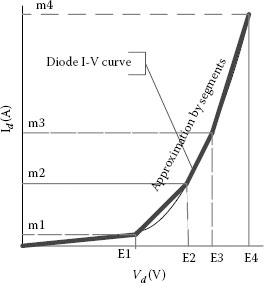
FIGURE 12.11 Real model of the PV.

FIGURE 12.12 Model of PV cell using Simulink.
12.5.2 MAXIMUM POWER POINT TRACKING
The power output of a solar PV module changes with the changing direction of the sun, with the solar insolation level, and with varying temperature. Hence, in order to get the maximum power from the solar PV, an interface should be added. A maximum power point tracker (MPPT) is used for extracting the maximum power from the solar PV module and transferring that power to the load. A dc/dc converter (step up/step down) serves the purpose of transferring the maximum power from the solar PV module to the load.
We choose the hill climbing method, which consists of observing the current and voltage at the output of the PV generator. Multiplying these two signals allows the power to be obtained. The value of the power is stored in two integrators in order to be used as two successive values in memory. Two successive values of the power can thus be compared to determine the power’s derivative. Then, using a JK toggle with a third integrator and a triangular signal allows the pulse width modulation control to be created and sent to the driver of the transistor (we use a P-channel metal–oxide semiconductor field-effect transistor [MOSFET]). Figure 12.13 shows a diagram of this technique.
The MPPT controller represents a good compromise between high performance and robustness. However, to achieve convergence in good conditions, whatever the power range and the algorithm, it is necessary that the power curves issued by the generator are constant or slowly varying. If this assumption is not respected (i.e., if there are some abrupt changes in operating conditions), then the system can diverge.
The principle of the MPPT controller is often based on the “elbow” of the PV characteristics. This is more or less trial and error, as shown by Figure 12.14. Indeed, the algorithm starts from a point located on the curve, let us say X1. After a while, the actual value on the curve (X2) is compared with the previous one (X1). If X2 > X1, then we move to X2, and this is repeated until the next term (Xn) is lower than the previous (Xn−1). At this time, we take an interval value from every lower point, and repeat from (Xn−1) to obtain the maximum power point (MPP) (X).
The MPPT controller consists of two distinct parts:
1. The control part, whose purpose is to determine the operating point, where the solar cell can transfer the power toward the batteries
2. The power part, which transfers energy between the solar panels and batteries
These two parts are also shown in Figure 12.15.
Now it is easy to transfer to the electronic schematic from the Orcad library, as shown in Figure 12.16.

FIGURE 12.13 Block diagram of the proposed MPPT controller.

FIGURE 12.14 Principle of operation of MPPT.
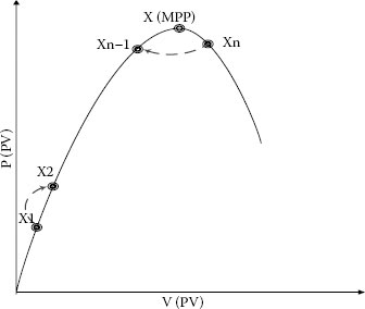
FIGURE 12.15 Block diagram of this type of control.
Some techniques for implementing an MPPT depend on the changing bias point and measuring changes in the output, while others use predetermined PV models. Table 12.4 shows all the MPPT methods that can be employed.
The perturbation and observation (P&O) method is one of the most popular MPPT methods because of its simplicity. The P&O method operates by making small incremental changes in voltage and measuring the resulting power change. By comparing the current power measurement with the previous power measurement, the P&O method selects the direction for the next perturbation. The P&O MPPT method can be implemented using a minimal number of components; however, its speed is limited by the size and the period of the perturbation [11]. Figure 12.17 shows the flowchart of this algorithm.

FIGURE 12.16 Proposed controller circuit diagram.
TABLE 12.4
Table of Various MPPT Methods
MPPT method |
|
1 |
P&O |
2 |
Hill climbing |
3 |
Incremental conductance |
4 |
Power feedback control |
5 |
Fractional short-circuit current |
6 |
Fractional open-circuit voltage |
7 |
Computational and lookup table |
8 |
Current sweep |
9 |
Fuzzy logic |
10 |
Array reconfiguration |
In a situation where the irradiance changes rapidly, the MPPT also moves along the right-hand side of the curve (see Figure 12.14). The algorithm takes this as a change due to perturbation, and in the next iteration it changes the direction of perturbation, hence moving away from the MPP, as shown in Figure 12.18.
The proposed MPPT scheme employing the P&O algorithm has been modeled and simulated using the MATLAB/Simulink® software. Figure 12.19 shows a block diagram of the developed PV system, consisting of a PV array and a boost converter circuit connected to a load and an MPPT controller. The PV array, with a capacity of 1 kW, consists of six PV modules associated with an MPPT controller. All this is simulated with conventional P&O under operating conditions of temperature 25°C and with varying insolation (0–1000 W/m2). The MPPT controller is based on the P&O method.
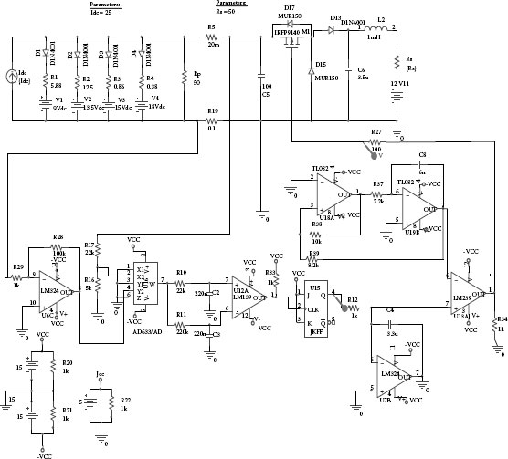
FIGURE 12.17 Flowchart of the P&O algorithm.
The whole PV system associated with an APF, as shown by Figure 12.19, has been simulated. The performance of the PV system using the P&O algorithm under a constant temperature of 25°C and a changing irradiance is shown by Figure 12.20. The irradiance values are 0, 400, 850, 950, 1000, 950, 850, 400, and 0 W/m2 at times 0, 0.01, 0.02, 0.03, 0.04, 0.05, 0.06, 0.07, and 0.08, respectively. It can be seen that the power issued by the converter is close to the PV power (Figure 12.21).
12.5.3 DIRECT CURRENT VOLTAGE OPTIMIZATION WITH THE PHOTOVOLTAIC SOURCE
The shunt APF and the PV array are connected back-to-back with a dc-bus capacitor. The dc-bus voltage controller maintains the average voltage across the dc-bus capacitor constant against variations in distribution source. As a result, the reference current injected into each phase allows the grid to gain more useful active power. The voltage across the capacitor must be constant and fixed at a predetermined value. Active power losses in the active filter (switches and output filter) are the main factors that may change the voltage. The average voltage across the capacitor energy storage must be regulated by adding the current fundamental asset in the reference currents.

FIGURE 12.18 Curve showing incorrect tracking of MPP by P&O algorithm under rapidly varying irradiance.
This stabilizes the dc voltage of the capacitor C of the three-phase voltage power inverter close to a continuous value. This has been verified by simulations, and the result can be seen in Figure 12.22.
12.5.4 CONTROL OF THE SWITCHING FREQUENCY
The switching frequency strongly depends on the coupling inductance Lf and on the width of the hysteresis band. The objective of this part is to propose a method to limit the frequency switching and make it independent of the parametric variations. For this, we propose to add to the expression of the surface a triangular signal with constant frequency and fixed amplitude. The principle of the method is illustrated in Figure 12.23.

FIGURE 12.19 Curve showing wrong tracking of MPP by P&O algorithm under rapidly varying irradiance.

FIGURE 12.20 Functional block of the whole system using the P&O technique.
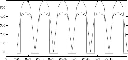
FIGURE 12.21 Power of the converter Pout-Boost, photovoltaic Ppv, and the ideal output Pideal.

FIGURE 12.22 Evolution of the dc-bus voltage around its reference value at 300 V.

FIGURE 12.23 Principle of limiting the switching frequency.
The proposed HAPF was simulated using the MATLAB/Simulink software. The system parameters that were used are summarized in Table 12.5. In the simulation, a diode rectifier with a dc-link capacitor and a smoothing inductor was used as a nonlinear load producing harmonics.
The complete scheme of the control structure that has been developed in this study to govern the APF supplied by a PV array and a capacitor is shown in Figure 12.23. Furthermore, the high-order harmonics are filtered from the source voltage and the source current.
The simulation results show that the source currents after compensation are almost sinusoidal and in phase with the voltage at the connection point. The harmonic spectra of the source current before and after compensation are presented in Figures 12.24 and 12.25, respectively. The THD of the current source (calculated on the first 30 harmonic orders) has decreased from 30.09% to 1.95%, and the load current harmonic components are greatly reduced. The dc-bus voltage is regulated to 300 V.
All results are shown in Figure 12.26 (the source, the current of load before and after the compensation, the current of the filter, and the dc voltage of the capacitor).
Figure 12.27 shows the spectrum of the source current Is in decibels. This spectrum allows us to see that the switching frequency varies between 5 and 10 kHz (see Figure 12.25). The average switching frequency is equal to 9.07 kHz. Low-frequency peaks are located between -40 and -60 dB. Above 4 kHz, the amplitudes of the lines are increasing, and once the frequency 7.5 kHz is reached, they are decreasing. Beyond 16 kHz, the spectrum is more regular, and rays have relative amplitudes below –50 dB.
TABLE 12.5
Matlab/Simulink Simulation Parameters
Utility voltage |
220√2(50 Hz) |
Source inductance |
0.65e-3 H |
Source resistance |
5−3 Ω |
Rectifier smoothing inductor |
1−3 H |
Rectifier smoothing resistance |
1.5 Ω |
Load inductance |
100−3 H |
Load resistance |
29*1.5 Ω |
Load capacitance |
2000–6 F |
Current control band |
1.8 A |
Sampling time |
10−6 s |
APF inductor |
2−3 H |
APF resistor |
0.005 Ω |
APF dc-bus capacitor |
450 V |
HPF capacitor |
5.01e-6 F |
HPF resistor |
20.46 Ω |
PV |
9 arrays |
Insolation |
1000 W/m2 |
Short-circuit current Isc |
5.45 A |
Open-circuit voltage Voc |
22.2 V |
Rated current IR at MPP |
4.95 A |
Rated voltage VR at MPP |
17.2 V |
Capacitance of the PV output |
2−3 F |
Resistance of PV output |
72.78 Ω |
This chapter has detailed a new technique for improving the efficiency of the sliding mode controller that is used to manage the PV energy in an autonomous shunt APF. In order to improve the reference current for compensating harmonics, a method to limit the switching frequency has been added and verified. The THD has been improved and the average switching frequency has only slightly increased. To reduce the switching frequency without changing the system settings, a technique based on the addition of a triangular signal to the switching surface has been proposed and tested (see Figure 12.23).

FIGURE 12.24 Compensation of harmonic currents with the sliding mode control.
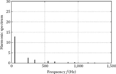
FIGURE 12.25 Harmonic spectrum of source current before compensation.

FIGURE 12.26 Complete diagram of the control structure.
A P&O MPPT has been implemented to maximize the PV output power. Through a boost dc-dc converter combined with the fastness and robustness of sliding mode control, the HAPF has good robustness and stability. A loop for capacitor voltage regulation is introduced into the sliding mode control; a good regulation effect is obtained for load variation in the dc bus. The simulation results confirm the effectiveness of the proposed scheme for wideband harmonics compensation and PV power handling capability (see Figures 12.27 and 12.28).

FIGURE 12.27 Spectrum of the source current Is in decibels.
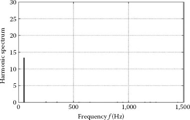
FIGURE 12.28 Harmonic spectrum of source current after the compensation.
HAPF |
Hybrid active power filter |
APF |
Active power filter |
PV |
Photovoltaic |
σ(x) |
Surface of sliding |
X |
System error |
u |
Control variable |
U |
Control vector |
2δ |
Bandwidth around the sliding surface |
f, g |
Functions of the nonlinear system |
C |
Coefficients of σ(x) |
1. H. Akagi, A. Nabae and A. Satoshi, Control strategy of active power filters using multiple voltage-source PWM converters, IEEE Transactions on Industry Applications, IA-22, 460–465, 1986.
2. D. Ould Abdeslam, P. Wira, J. Merckle, D. Flieller and Y.-A. Chapuis, A unified artificial neural network architecture for active power filters, IEEE Transactions on Industrial Electronics, 54, 61–76, 2007.
3. S. Rahmani, A. Hamadi, N. Mendalek and K. Al-Haddad, A new control technique for three-phase shunt hybrid power filter, IEEE Transactions on Industrial Electronics, 56, 2904–2915, 2009.
4. A. Hamadi, S. Rahmani and K. Al-Haddad, Sliding mode control of three-phase shunt hybrid power filter for current harmonics compensation, in Proceedings of the IEEE International Symposium on Industrial Electronics (ISIE), pp. 1076–1082, 4–7 July, Bari, 2010.
5. A. Blorfan, J. Mercklé, D. Flieller, P. Wira and G. Sturtzer, Sliding mode controller for three-phase hybrid active power filter with photovoltaic application, Smart Grid and Renewable Energy, 3, 17–26, 2012.
6. B. Cheng, P. Wang and Z. Zhang, Sliding mode control for a shunt active power filter, in Proceedings of the Third International Conference on Measuring Technology and Mechatronics Automation (ICMTMA), pp. 282–285, 6–7 January, Shanghai, 2011.
7. D. Wenjin and Yu. Wang, Active power filter of three-phase based on neural network, in Proceedings of the Fourth International Conference on Natural Computation, ICNC ‘08, pp. 124–128, 18–20 October, Jinan, 2008.
8. A. Blorfan, D. Flieller, P. Wira, G. Sturtzer and J. Merckle, A new approach for modeling the photovoltaic cell using Orcad comparing with the model done in Matlab, in International Review on Modelling and Simulations (IREMOS), vol. 3, pp. 948–954, October 2010.
9. G. Sturtzer, Projet Simulation Panneaux Photovoltaïques, p. 8, 2009.
10. S. Chowdhury, S.-P. Chowdhury, G.A. Taylor and Y.H. Song, Mathematical modelling and performance evaluation of a stand-alone polycrystalline PV plant with MPPT facility, in Proceedings of the 2008 IEEE Power and Energy Society General Meeting—Conversion and Delivery of Electrical Energy in the 21st Century, pp. 1–7, 20–24 July, Pittsburgh, PA, 2008.
11. M. Veerachary, T. Senjyu and K. Uezato, Voltage-based maximum power point tracking control of PV system, IEEE Transactions on Aerospace and Electronic Systems, 38, 262–270, 2002.