
CONTENTS
6.2 Hybrid Semiconductor X-Ray Imaging Detector Materials and Contacts
6.3 ASIC Technology for Hybrid Pixel Detector Readout
6.7 Dead Areas in Modular Systems
6.8 Through-Silicon Via (TSV) for I/O Connection Needed for Low Dead Areas
6.9 3DIC Technology Advantages
Area-array imaging detectors are ubiquitous in our everyday lives and in science instrumentation. For imaging IR, visible, and UV photons, the usual approach taken is to use focusing optics to concentrate the light onto a small imaging area and to use the smallest pixels possible to reduce the cost of the imaging detector. This is usually true in science experiments as well as commercial cameras. The modality for detecting x-rays is very different. In most cases it is impossible to focus the x-rays, and large-area detectors are required. This is true for x-ray photon and particle detectors in high-energy physics, space science, and synchrotron applications. Many applications can use large flat panels [1] with deposited scintillators or scintillating screens. Amorphous silicon screens have been very successful in medical and security applications as well as science but do have limitations in speed and several other performance criteria [2]. Complementary metal–oxide–semiconductor (CMOS) sensors have recently surpassed charge-coupled devices (CCDs) for many applications and can now be constructed on a wafer scale [3]. Even with these wafer-scale sensors, there is a requirement to tile these to create larger arrays. Up to a certain size, this is relatively easy, as the detectors can be three-side-butted and connected to scintillator screens. The readout can be performed on one edge using conventional wire bonding and the sensor area connected to a stable substrate which also allows cooling if required (Figure 6.1).
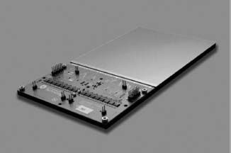
FIGURE 6.1 Three-side-buttable LASSENA CMOS sensor of 140 × 140 mm2 with 50 μm pixels mounted on readout card.
These CMOS sensors are also used in this configuration for the direct-conversion mode of detecting x-rays using diodes integrated in the CMOS technology to convert the x-rays to electrons. This is usually restricted to low-energy x-rays (<10 keV) and can suffer from radiation damage effects. Overall, flat-panel detectors and CMOS sensors have been very successfully integrated into arrays using large-area modules. The situation with direct-conversion semiconductor detectors using thicker conversion layers is very different. This requires the use of separate conversion layers of thick silicon or high-atomic number material bonded to the readout electronics in a so-called hybrid configuration. The process technologies and interconnect for these hybrid sensors are much more complicated.
6.2 HYBRID SEMICONDUCTOR X-RAY IMAGING DETECTOR MATERIALS AND CONTACTS
X-rays interact inelastically with matter in three ways: photoelectric, Compton, and pair production [4]. These energy-loss mechanisms all eventually produce thermalized electron–hole pairs in the conduction and valence bands of the semiconductors. The basic conversion process consists of the electric field of the x-ray photon transferring energy to a bound electron in the material. This can, for instance, be a k-shell electron, which causes it to be ejected out of the atom. This resulting photoelectron (and also subsequent Auger electron) interacts with the electric field in the crystal lattice, elevating electrons to the conduction band and leaving holes in the valence band of the semiconductor. This is a statistical effect, producing electron–hole pairs by multiple photon–phonon interactions. On average, one electron–hole pair is produced by 3.6 eV of the photoelectron energy in silicon. These mobile carriers drift in an applied electric field across the detector. In semiconductor detectors, a large voltage can be applied across the crystal to cause these charge carriers to drift to the anode and cathode sides of the detector. As the charge carriers move, they induce a charge on electrodes on the anode and cathode sides of the detector. It is this induced signal that is measured by the preamplifiers on application-specific integrated circuits (ASICs), as explained in Section 6.3. Detectors can have thousands or millions of contacts and similar numbers of amplifier channels. In most cases, the amplifiers are fabricated on silicon ASICs, with each amplifier connected directly to the detector contact, as explained in Section 6.4.
Silicon has been used as a good conversion material to convert x-rays into charge carriers. It has a large bandgap, so very few electron–hole pairs are thermally produced at room temperature. Blocking contacts can be produced, which further reduce unwanted leakage currents. The bandgap is sufficiently low that the photoelectron produces many carriers. Good crystals with low trapping/recombination centers are produced, so that the charge carriers produced can drift large distances in the material. The advanced technology allows nearly any geometry of pixels and contact structures. The photoelectric effect dominates in most materials up to a few tens of kiloelectronvolts. High-resistivity silicon detectors are typically limited to about 500 mm thick material (at reasonable full-depletion voltages), and this thickness can absorb most photons up to about 15 keV by the photoelectric effect. Unfortunately, above this energy silicon becomes essentially transparent. Photoelectric absorption increases as the fourth power of the atomic number, so higher-atomic number elements can absorb x-rays more efficiently. What we would like is a high-Z material (for good absorption) with a high bandgap (for low leakage) and good crystal quality with good charge transport (high mobility–lifetime product). As one would expect, the perfect high-Z material does not exist. Germanium is nearly a perfect material, with a reasonable atomic number and superb charge transport, but it has a low bandgap of 0.66 eV, which requires cooling to cryogenic temperatures to stop unacceptable leakage current. GaAs and HgI have been proposed for a long time [5], but it has not been possible to produce reliable material with unpopulated bandgaps. Another continuing problem with epitaxial GaAs has been the need to grow detector-grade material on thick substrates, which then have to be removed. This process has been a technical barrier to development of material with good conversion efficiency. Currently, highly doped bulk material has acceptable performance in some applications [6]. CdTe and CdZnTe are currently the most favored crystals for this application. The bandgap is about 1.4 eV, increasing with increasing zinc concentration. The advantage of a wider bandgap is higher resistivity and lower leakage currents. As a rule of thumb, the energy to produce an electron–hole pair in semiconductor material is about three times the bandgap, and this holds for Cd(Zn)Te. The charge transport over a few millimeters is acceptable, and growth techniques have now improved to give reliable material [7,8,9]. The x-ray absorption [10] is shown in Figure 6.2: several millimeters of material can efficiently convert 100 keV photons and above.
Area-array detectors built with CdTe or cadmium zinc telluride (CZT) [11,12] use typically 1–10 mm thick material, depending on the energy of the incident photons and the efficiency required. Cd(Zn)Te detector material is now grown with good quality. Bulk material in boules 4 in. in diameter can be obtained by several Bridgeman techniques, the traveling heater method, or multitube physical vapor transport. Resistivities of 1010 to 1011 ohm-cm and mobility–lifetime products of 1 × 10⁻² to 3 × 10⁻² V cm−1 s−1 are achieved (Chapter 3). There is now good availability of high-quality detector material, but there are still many academically interesting and technically challenging issues to be solved in creating reliable electrical contacts to the material.
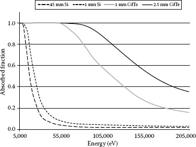
FIGURE 6.2 X-ray absorption against photon energy for different thicknesses of CdTe and Si.
Indium and aluminum contacts (cathode and anode, respectively) are used for good-quality Shottky blocking contacts on CdTe [13]. The advantage of these is reduced leakage current, but blocking the thermally generated and signal generated carriers causes issues due to so-called polarization or field collapse below one of the contacts in the bulk of the material [14]. This can be controlled by pulsing the bias supplies if the problem is not too pronounced. Gold and platinum are used as more ohmic contacts to both CZT and CdTe material. There are still problems of uniformity, injection of current, and stability of contacts. At the present time, singleelement or large pad (1–2 mm) detectors are available with good uniformity from material suppliers and other fabricators. Small pixel detectors with lithographic features below 250 μm are very much more difficult to obtain [15]. Detectors with small pixels (50–250 μm pitch) are required due to their imaging resolution, but also because the small-pixel effect allows single carrier-type readout due to the high weighting field around the pixels. This gives very good spectroscopic capability and reduces the effects of the poor hole mobility in Cd(Zn)Te. In CZT and CdTe, these small pixels are hard to obtain commercially. GaAs detectors are produced with small pixels due to the more advanced processing technology. This modality is one area where GaAs detectors have an advantage over other high-Z detector materials. Germanium has historically not been available with pixelated contacts, but in the last few years strip and pixel-contacted detectors have been developed [16]; however, there is still the huge issue of running the detector at liquid nitrogen temperature and readout electronics at a higher temperature.
6.3 ASIC TECHNOLOGY FOR HYBRID PIXEL DETECTOR READOUT
Clearly, for large-area imaging detectors with many imaging pixels a high level of segmented multichannel readout is needed. Several decades ago, the only way to achieve this was via massive fan-out schemes to route signals to discrete low-density electronics. At the present time, CMOS technology allows us to build very dense low-power electronics with many channels that can be bonded directly to the conversion/sensing medium [17]. There are different requirements for the CMOS technology used for the analog front-end signal processing, as opposed to that for the digital signal processing and off-chip communication. For the analog part of the electronics, there is a requirement for a robust technology that has low electronic noise in terms of thermal noise, junction leakage and capacitance, and flicker noise. Also, there is a need for large power-supply voltages (3.3–5 V) to accommodate a wide dynamic range. For digital signal processing and communication, there is a requirement for very high-speed, high-density, low-power technologies that are compatible with the more modern low-voltage supply, deep submicron processes.
There seems to be a technology optimum at present at around 0.35–0.25 μm minimum feature size for the analog requirements. These CMOS processes have robust insulated-gate field-effect transistor (FET) oxides so that input protection circuits can be optimized for noise performance, and also so that they have wide dynamic range and low noise coefficients. The additional advantage of these technologies is that they are relatively cheap, costing less than EUR 100,000 for an engineering run of a new design and EUR 2000 per wafer. This technology is also relatively easy to design with and has acceptable die sizes of about 20 × 20 mm2. Obviously, the large feature size limits the complexity of circuitry that can be integrated in a pixel, but the device performance compensates for this. Surprisingly, even with the relatively thick gate oxides, the total dose radiation hardness of these technologies can be acceptable [18], and, with suitable consideration of substrate biasing, latchup-free designs can be achieved.
In comparison, the digital signal-processing side of the measurement chain can benefit from the rapid development of deep submicron processes. Science applications have used 0.25, 0.18, and 0.135 μm, and are now using 65 nm [19] and proposing 22 nm technologies for digital components. These technologies are well suited to high-speed analog-to-digital converter (ADC) architectures and to very fast data manipulation for data sparsification and packaging. The technologies have their own limitations in terms of gate-oxide thickness, noise, and cost. The nanometer gate oxides and small interdevice distances reduce the power supply range and can introduce noise problems. A major practical problem is the cost of a mask set and engineering wafer batch, and also the design complexity, which increases design engineer costs. A full ASIC development can easily cost over EUR 1,000,000 and extend over 2 years, which can be a significant problem for the budget of some scientific experiments.
These high-density processes will be important for new devices, and SiGe and multigate FET processes will expand the range of processing architectures we can integrate close to the front end of detector systems. Also, new auto-gain switching front-end circuits [20] allow wide dynamic range without needing large power-supply voltages. In Section 6.9, we will discuss how we can use mixed technologies to optimize the use of the strong points of these different technologies.
Pixel detectors require a direct connection from the pads on the sensor material to the bond pads on the ASICs. Figure 6.3a shows a simple pad geometry for connection to the detector where the pixel pitch on the readout ASIC is the same as the detector pixel pitch. It is also possible to fan out the connections on the detector with multilevel metal routing on the detector, as shown in Figure 6.3b. This has to be done very carefully, as there is huge scope for signal cross talk. With integrating readout and synchronous input signals [21], where the signal is totally removed from the detector, this might not be a problem, but transients can still upset thresholds in these systems.
The pitch of x-ray imaging systems currently ranges from about 50 μm to 1 mm. Bump bonding is used to connect the detector pixels to the ASICs. There are many different technologies to do this, depending on the requirements of the detectors and environmental constraints.
The industry-standard area bump bonding method is to deposit solder onto underbump metalization on the pads of the detector and ASIC and then to align the two and heat them to reflow the solder. Various solders are used, including lead–tin, bismuth–tin, indium alloys, and silver alloys, depending on the temperature to reflow and the operating temperature required [22]. Typically, these materials require 240°C–140°C to reflow. Indium is used in either a lower-temperature reflow process or straight compression bonding [23], and gives good results, but cannot be used if high operating temperatures will ever be experienced. With all these processes, either fluxes or special gas environments, including nitrogen, hydrogen, or formic acid, have to be used to ensure good contact between parts. These processes can enable the use of 10 μm bond diameters, which allows 25–50 μm pixels to be connected [24]. Another method, used particularly for larger-pixel (150–250 μm) CZT detectors, is gold stud and silver-loaded epoxy dots. The gold studs are either bonded or deposited on the ASIC part, and the silver-loaded epoxy is screen printed on the detector. A process for this is used by our group at Science & Technology Facilities Council (STFC) for connection of CZT. After alignment, the unit is heated to set the epoxy. This can be done at low temperatures of 45°C to 120°C so that the detectors are not affected. CZT is a very sensitive crystal, and it has been seen that temperatures of around 150°C can cause movement of impurities and damage sites, which affect detector performance. This method uses 50 μm gold studs, which gives large distances between the components and is good for capacitance and stress relief. For all these processes, there is the option to use an underfill after bonding to strengthen the connection and seal against corrosion.
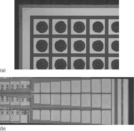
FIGURE 6.3 (See color insert) (a) Hexitec CdTe 250 μm pitch pad geometry with silver glue dots. (b) XFEL LPD redistributed bonding pads 250 × 400 μm2 pitch (left) to the 500 μm pitch pixels on a two-layer interconnect silicon detector.
Other area-interconnect methods have been used, such as direct gold-to-gold and indium pillar contacts. Also, solid liquid interface diffusion (SLID) bonding can be used. This Cu–Sn process leaves a bond that is robust to subsequent processing up to 400°C. This is being used in three-dimensional integrated circuits (3DIC) [25] and silicon-interposer technology, but could be a prospect for high-strength detector-to-ASIC connection.
A serious issue with hybrid detector systems is stress produced in the detector material and to the interconnection surfaces [26]. One inherent issue is the different coefficient of thermal expansion of the different components. The bump bonding interconnection processes above require the module to be heated to 100°C–200°C and above. The device might then be required to operate at 0 to −10°C temperature for best performance (with CdTe). With large detectors of 20 mm length and above, this causes a considerable strain to be set into the interconnection face. With a CZT detector connected to silicon, this is several microns of linear change over a few centimeters of detector with 100°C temperature change. Either the bumps have to accommodate this or the material is stressed and the structure could bend like a bimetallic strip or break. None of these is good, but considering using the minimum processing temperature and allowing the bumps to take the deformation is the least bad option. With CZT, there is certainly an additional problem with inbuilt stress, as this can cause residual internal electric fields around the pixels as well as affecting the long-term reliability of the fragile electrical contact interfaces.
Another problem is the connection of the ASIC to the cooling/alignment block used to support the ASIC to the instrument. Aluminum would be a very convenient mounting substrate, but has a very different CTE from silicon. Molybdenum is often used, as it has a good CTE match to silicon (even better to CZT) and is also a good thermal conductor. It is, however, quite expensive. A good option we have found is to accept the mismatch with a metallic mounting plate but use a compliant heat transfer tape. We had a spectacular failure of a 54 × 54 mm2 area CMOS detector when hard glued to a copper block but complete success mounted with compliant tape. With smaller ASICs, the epoxy glue is quite adequate, but it can still stress the silicon and affect reliability.
There are several intrinsic noise processes that limit the performance of pixelated detectors. These can be split into sources related to the detector and processes related to the way the electronics reads out the detector [27]. These processes define the ultimate limit of performance, but there are many ways that the architecture can be designed inappropriately so that these are not the dominant effect.
Assuming all environmental noise is eliminated, the fundamental front-end-related noise can be summarized as equivalent noise charge (ENC) given by Equation 6.1:
(6.1) |
where:
(bt, bs, bf) |
= |
coefficients calculated for a particular shaping filter |
ctot |
= |
capacitance of the detector and tracking |
i |
= |
leakage current of the detector |
gm |
= |
transconductance of the input FET of the amplifier |
T |
= |
temperature |
k |
= |
Boltzmann’s constant |
Definition of terms are fully explained in [27].
The ENC is the signal charge you would have to inject onto the detector in order to produce an output signal equivalent to the rms noise you measure at the output of the system. The terms for the individual ENC components are added in quadrature to give the total noise. This method of addition is required as statistically independent noise sources add as powers so we add the squares of the voltages. These noise contributions from the electronics affect the accuracy with which the signal can be measured. The signal produced in the detector has an intrinsic statistical noise. In semiconductor detectors, ionizing radiation produces a number of charge carriers, as described in Section 6.2. With a stochastic process, one would expect the noise on the number of carriers to be the square root of the number of carriers. In fact, because of the carrier-formation process, the signal noise is better than this square root by a factor known as the Fano factor [28]. This term is the ultimate or Fano limit of resolution of the detector, but has to be added in quadrature to the electronic noise contributions. Lowering the bandgap increases the number of carriers, which improves the accuracy of measurement; this is one reason why Ge detectors have good resolution. The down side of a low bandgap is that the thermally generated leakage current can offset this advantage. High-Z conversion materials all have other noise mechanisms and inhomogeneity, which produce signal uncertainty problems. In CZT, the major problem areas can be small inclusions [29] and other bulk and contact nonuniformities, which cause very localized changes in charge-carrier transport efficiency. This creates fixed-pattern noise, which unfortunately cannot always be removed in subsequent processing. Other problems occur due to charge sharing across pixels [30]. This can cause additional signal uncertainty problems related to the exact detailed system parameters and subsequent signal processing.
If one inspects the basic ENC formula, one can obtain several design objectives. As the thermal noise (bt) decreases with shaping time and leakage current (shot) noise (bs) increases with shaping time [31], there is an optimum shaping time for a detector:
(6.2) |
Because of the formula for the thermal noise of an insulated-gate FET (IGFET):
(6.3) |
one can optimize against cin and obtain an optimum input FET gate capacitance of 1/3 to 1 times the total input detector capacitance [32]. This so-called matching condition sets a good criterion for the input circuit design.
Further inspection of the ENC formula shows an even more important design driver. If the leakage current is reduced, the leakage noise reduces. If the detector capacitance reduces, the thermal noise reduces. The way to achieve both of these together is to segment the detector into smaller pixels. A limit is reached where capacitance actually increases, but to first order having many pixels improves measurement accuracy. Also, as there are more amplifier channels, the possible bandwidth to measure signal photons is increased. Another practical limitation is reached when the pixel size is so small that charge-carrier clouds spread across multiple pixels, and this charge-sharing effect then has to be resolved by more complicated signal processing. Overall, fine pixel systems have the potential to be lower noise and faster than single-channel systems.
Several direct-conversion x-ray imaging systems have been built using a photon-counting technique, including Medipix, Pilatus, and XPAD [33]. Typically, this involves the front-end electronics amplifying the charge signal and then using a discriminator to count the number of hits in the pixel with a value above a set level. Some ASICs have the capability to have several discriminators and several counters to get a rudimentary spectroscopy [34]. To achieve a true spectrum, the threshold has to be scanned during repeated experiments. Another method used by STFC is to amplify the signal, output the analog signal for every photon incident in the pixel, and perform an ADC conversion on this value [35]. The advantage of this is that the position and energy of every charge cloud are measured, allowing an effective improvement in efficiency and good correction of charge sharing. The advantage of this hyperspectral data with very good spectral resolution is that there is a new richness in the data to allow advanced imaging techniques [36].
An important technology aspect of array detectors is the close integration of the electronics to the semiconductor detector material. As we have seen, this is important for capacitance and other noise-injection possibilities. With wire-bonded detectors, it is possible to have thermal breaks between the electronics and the detectors [37].
The intimate connection of the electronics to the detectors in array detectors means that the electronics and detector are essentially thermally coupled. The low-noise front ends and complex electronic processing generate a lot of heat: 0.5 W cm−1 is certainly possible. CZT semiconductor detectors will work at room temperature, but the leakage increases rapidly with elevated temperature. In order to operate the detectors efficiently, some form of heat removal is required. In most systems, this is only achieved by attaching the ASICs to a cooling substrate. The mechanics and materials used for this are different in different systems, including circulating binary ice, high-pressure evaporative liquids [38], Peltier devices, forced air cooling, heat pipes, and off-detector cooling. The technologies vary, but the consequence is the same: the back of the detector becomes very congested. The cooling takes place in exactly the space where one would like to route interconnections to control and take data from the ASICs. An example of the cooling is shown in Figure 6.4, but many other configurations are used [39].
6.7 DEAD AREAS IN MODULAR SYSTEMS
As already stated, large-area hybrid detector systems have to be built from multiple modules. There is a general requirement to reduce the dead areas between modules for cosmetic reasons in the image as well as necessary science issues for full image coverage. Several hybrid systems are built using conversion material directly bump bonded to ASICs. In order to read out these ASICs, at least one edge of the ASIC has to be exposed (not covered by conversion material) so that wire bonds can be made to pads on the surface. An image of this is shown in Figure 6.5.

FIGURE 6.4 Cooling block of the multimodule Hexitec system.

FIGURE 6.5 Wire bonds connecting the ASIC to the readout board. The detector (top) cannot be close to these wire bonds, so there is an area of the ASIC not covered by the detector. This causes a large dead area between this detector and the next.
A gap has to be left between detectors to allow room for these wire bonds and the connection board; typically this is about a minimum of 1–2 mm. This has two consequences: there is a dead area for the detector, and also the ASIC is directly exposed to radiation, which can have radiation-damage consequences. One possibility is to have a roof-tile geometry for the detectors, shown in Figure 6.4. This allows the wire-bonded area of one ASIC to be covered by an active detector area of the next detector. This is very effective but produces a detector surface which is not a flat surface normal to the incident x-rays. Section 6.8 describes a new method to allow full coverage of the detector plane and also to have a flat detector. All direct-conversion detectors need a high-voltage bias to be connected to the back of the detector. This can also be done using the same method as the wire bond to the ASIC I/O pads, as shown in Figure 6.6.
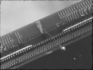
FIGURE 6.6 Wire bonds to the exposed I/O pads on the fourth side of the ASIC, with single HV connection to the back of the detector.
The other three edges of the ASIC, not required for bonding, can be covered by the detector material, so that the detectors can be spaced as close as mechanically allowed. The edges of the detector also cause dead areas. Semiconductor detectors have to be cut from a larger wafer, which nearly always causes the edge material to have significantly different properties from the bulk material. In silicon, a diced edge has crystal damage, which shorts the top and bottom of the edge together. So-called edgeless or active-edge silicon detectors have been built by very specifically fabricating the edges [40]. With GaAs and CdTe detectors, usually there is a guard band on the edges of the detector to stop the edge leakage current from entering the edge pixels. STFC have been working on active-edge CdTe detectors, which have shown that good counting efficiency and spectroscopy can be achieved without guard bands, allowing very close packing of detectors [41]. Similar results are shown on Medipix detectors with very small intermodule dead regions [42].
6.8 THROUGH-SILICON VIA (TSV) FOR I/O CONNECTION NEEDED FOR LOW DEAD AREAS
STFC have built an x-ray imaging spectroscopy readout system based on CdTe detector material. A 20 × 20 × 1 mm3 crystal is bonded to a Hexitec ASIC with gold stud bonds to 80 × 80 pixels of the detector. Each pixel is 250 × 250 μm and has an amplifier and a peak-track-and-hold circuit. This allows the energy of every photon to be recorded and measured with subkiloelectronvolt full width at half maximum (FWHM) accuracy from 4 to 200 keV and above [43]. The first versions of the ASIC allow the detector modules to be butted on three edges with only a 170 μm gap between detectors. The fourth edge of the ASIC has wire bonds, which precludes butting the detectors in a flat geometry. A similar restriction has compromised the design of the popular Dectris Pilatus detector. The only way to avoid these wire bonds restricting the coverage of the ASIC is to read out the ASIC from the back of the detector. Several methods are proposed, but STFC has chosen an approach whereby the wire bond pads are shielded with a metal plane on the top of the ASIC to stop electromagnetic injection into the detector. The I/O bond pads are then read out with through-silicon vias (TSVs) [44]. The process involves thinning the wafer to 100 μm so that it is still mechanically robust and then etching a TSV from the back to connect to the back of the metal bond pad. The TSV is plated with metal, and a pad of the same metal is fabricated on the back of the ASIC. Then an almost identical, but mirrored, wire-bonding method is used to connect to the back of the “4S” ASIC, as shown in Figure 6.7.
With this geometry, it is possible to extend the active CdTe over the whole of the front surface of the ASIC. This allows large-area coverage with four-side butting and only very small dead regions on all edges of the detector modules.
6.9 3DIC TECHNOLOGY ADVANTAGES
CMOS ASIC technology has progressed over the decades with the relentless Moore’s law. However, as we approach the 22 nm feature-size regime it is believed that simple dimension scaling will not be sufficient. This is where so-called 3DIC technology will be an important next-generation technology [45]. The objective of 3DIC technology is to distribute the signal processing on several layers of silicon and then connect the layers by TSV technology as shown in Figure 6.8. The advantage comes partly from simply having multiple layers of silicon but mostly from the immense connection density. This mimics, as a biological analogy, the animal nervous system, with the immense processing capability produced by the billions of three-dimensional neural connections. The drive for this technology is to scale processing power, but this will be also extremely useful for area-array detectors. As we have seen, different CMOS processes have advantages for either analog or digital functions. Connecting them together allows the best technology to be used for the analog process and the best for the digital process. Typically, connections would be made between the layers within each pixel. The signal from the analog layer is amplified and transferred using a small via from this top layer through the thinned (20–50 μm) silicon substrate to the digital layer below.

FIGURE 6.7 Wire bonding to redistributed pads on the back of a “4S” ASIC. Each pad has a TSV through the thinned 100 μm ASIC.
Several demonstration prototypes of this technology are being trialed in the science community [46,47]. The 3DIC technology is only starting to be used in the commercial sector [48], and the first large investments in plant are only now being made, to achieve capability in the next few years. STFC has a program to investigate the feasibility of 3DIC technology for imaging detectors [49]. We have used the analog front-end part of the Hexitec CZT readout ASIC as the pixel for the analog layer. The amplified output from each 250 μm pixel is then sent via a TSV to a peak-track-and-hold and Wilkinson ADC circuit on each pixel of a lower digital ASIC. The aim of this is to digitize all the signals from the detector on one 3DIC ASIC. The analog and digital ASICs are both fabricated on an Austrian Micro Systems (AMS) 0.35 μm CMOS process to reduce the cost of the trial. The tungsten via technology and the SLID interconnection between the wafers are performed by EMFT in Munich [50]. This technology has rather large TSVs of 3 × 10 μm and requires a large connection pitch due to the large size of the SLID pad technology, shown in Figure 6.9. The advantage of the process is that it is a via-last (or back-end-of-line) process, so that any CMOS process can be used, and possibly different technologies for the two layers. TSV processing can induce large strain in the silicon, which can affect the active circuitry, particularly with modern processes that rely on strain in the FET for high-performance operation. The relatively large space around the via in this technology is an advantage in this respect.

FIGURE 6.8 3DIC stacking showing bump bond from detector to active surface of the thin ASIC, and the TSV through to the SLID connection to the active layer of the thick ASIC. In this case, there is a SLID support under the bump bond.
The aim of 3DIC technology for imaging detectors would be to eventually reduce the vias to a few microns and have pixel sizes in the range of 50–100 μm. This would allow a fine-pitch detector with smart signal processing in each multilayer pixel. In order to do this, we will probably have to wait for extremely thin silicon layers and the introduction of front-end-of-line processes, which have the vias inserted in the silicon, before active devices are fabricated. These processes will be very expensive and will probably be driven by the digital processing and communications markets. This will mean that the technologies might not be ideal for all science applications. Until then, via-last and silicon-interposer [51] technologies will be used, which will allow mixed technologies and cheaper cost, if not ideal in other respects. The alternative silicon-interposer technology has been used in the large pixel detector (LPD) for the x-ray free electron laser (XFEL) European x-ray source [52]. This is a useful technology but is widely recognized as a stepping stone to full 3DIC technology for these imaging applications.
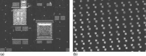
FIGURE 6.9 (a) The four 3 × 10 μm2 vias are shown in the 3DIC via area. The aluminum contact to this can be seen entering from the top. The other large square is the bump bond pad for connection to the detector. (b) The SLID bond pairs connecting to the digital ASIC. One of the pair is the TSV connection and the other is a pad under the bump bond pad for support.
Silicon wafers have to be very flat in order that photolithographic and other processes can be reliably performed on the active surface. This dictates the use of very thick wafers of 700–1000 μm for dimensional stability. These thick wafers are perfect for subsequent bump bonding processes to detectors that require a relatively relaxed flatness of a few microns across the ASIC. In conventional solder bump bonding of silicon to detectors, the bonding can be done at the wafer level or at the ASIC level. When the wafer is thinned, the highly stressed processed side of the ASIC causes the whole wafer to distort. In 3DIC processing, the only way to obtain very thin and flat wafers is to attach them to handle wafers and perform all the grinding and interconnect steps while the thin wafer remains on the handle wafer.
If we want to use these devices for imaging detectors, the final stack has to have at least one thick substrate to remain flat enough for the subsequent bonding to detectors. The stress in the stack still remains, but at least the ASICs will be flat enough to be bonded.
An even more difficult challenge is when TSVs are used on a single-layer device to redistribute the I/O connection from the ASIC bond pads to the back of the wafer, as described in Section 6.8. This is particularly useful for four-side-bonded area-array detectors with very small dead areas. At STFC, we have used single layers thinned to 100 μm and seen that the stress in the ASIC causes them to distort over an area of 20 mm. The solution to this might be to firmly bond them to the detector. The detector and the bonding will then form the support for the structure.
1. S. Kasap, Amorphous and polycrystalline photoconductors for direct conversion flat panel X-ray imaging sensors, Sensors (2011), 11, 5112–5157.
2. J. A. Seibert, Flat panel detectors: How much better are they? Pediatric Radiology (2006), 36(Suppl. 2), 173–181.
3. I. Sedgwick, LASSENA: A 6.7 MegaPixel, 3 sides buttable wafer-scale CMOS sensor using a novel grid-addressing architecture, in Proceedings of the 2013 International Image Sensor Workshop, June 12–16, Snowbird, UT, (2013).
4. G.F. Knoll, Radiation Detection and Measurement. Wiley, New York.
5. B.E. Patt, Development of mercuric iodide detector array for medical imaging applications, Nuclear Instruments and Methods in Physics Research Section A (1995), 366, 173–182.
6. O.P. Tolbanov, GaAs structures for X-ray imaging detectors, Nuclear Instruments and Methods in Physics Research Section A (2001), 466, 25–32.
7. H. Chen et al., Characterization of large cadmium zinc telluride crystals grown by traveling heater method, Journal of Applied Physics (2008), 103, 014903.
8. J.T. Mullins et al., Vapor-phase growth of bulk crystals of cadmium telluride and cadmium zinc telluride on gallium arsenide seed. Journal of Electronic Materials (2008), 37, 1460.
9. H. Shiraki et al., Improvement of the productivity in the THM growth of CdTe single crystal as nuclear radiation detector, IEEE Transactions on Nuclear Science (2009), 56, 1717–1723.
10. E. Gullikson, X-ray interactions with matter, The Center for X-Ray Optics. http://henke.lbl.gov/optical_constants/.
11. P. Seller et al., Pixellated Cd(Zn)Te high energy X-ray instrument, Journal of Instrumentation (2011), 6, C12009.
12. W. Kaye et al., Calibration and operation of the Polaris 18-detector CdZnTe array, in 2010 IEEE Nuclear Science Symposium Conference Record (NSS/MIC), October 30–November 6, Knoxville, TN. IEEE, (2010), pp. 3821–3824.
13. T. Takahashi et al., High-resolution Schottky CdTe diode detector, IEEE Transactions on Nuclear Science (2002), 49, 1297–1303.
14. A. Cola, The polarization mechanism in CdTe Schottky detectors, Applied Physics Letters (2009), 94, 102113.
15. M.C. Veale, S.J. Bell, P. Seller, M.D. Wilson and V. Kachkanov, X-ray micro-beam characterization of a small pixel spectroscopic CdTe detector, Journal of Instrumentation (2012), 7, P07017.
16. Semikon Detector GmbH, Germany.
17. R. Ballabriga, Medipix3: A 64 k pixel detector readout chip working in single photon counting mode with improved spectrometric performance, Nuclear Instruments and Methods in Physics Research Section A (2011), 633 (Suppl. 1).
18. F. Faccio, Total dose and single event effects (SEE) in a 0.25 μm CMOS technology. in 4th Workshop on Electronics for the LHC (CERN-LHC-98-036), September 21–25, Rome. CERN, (1998), p. 105.
19. S. Bonacini, P. Valerio, R. Avramidou, R. Ballabriga, F. Faccio, K. Kloukinas and A. Marchioro, Characterization of a commercial 65 nm CMOS technology for SLHC applications, Journal of Instrumentation (2012), 7, P01015.
20. J. Becker, Challenges for the adaptive gain integrating pixel detector (AGIPD) design due to the high intensity photon radiation environment at the European XFEL, Proceedings of Science Vertex (2013), 2012, 012.
21. European XFEL LPD detector, Hamburg. http://www.xfel.eu/.
22. W.K. Choi et al., Development of low temperature bonding using In-based solder, in 58th Electronic Components and Technology Conference, May 27–30, Lake Buena Vista, FL. IEEE, (2008), pp. 1294–1299.
23. H. Heikkinen et al., Indium-tin bump deposition for the hybridization of CdTe sensors and readout chips, in 2010 IEEE Nuclear Science Symposium Conference Record (NSS/MIC), October 30–November 6, Knoxville, TN. IEEE, (2010), pp. 3891–3895.
24. P. Norton, HgCdTe infrared detectors, Opto-Electronics Review (2002), 10(3), 159–174.
25. P. Ramm, 3D-IC fabrication challenges for more than Moore applications, in Workshop Manufacturing and Reliability Challenges for 3D ICs using TSVs, September 26, San Diego, CA. Sematech, (2008).
26. W. Sang, Primary study on the contact degradation mechanism of CdZnTe detectors, Nuclear Instruments and Methods in Physics Research Section A (2004), 527, 487–492.
27. P. Seller, Noise analysis in linear electronic circuits, Nuclear Instruments and Methods in Physics Research Section A (1996), 376, 229–241.
28. A. Owens, On the experimental determination of the Fano factor in Si at soft x-ray wavelengths, Nuclear Instruments and Methods in Physics Research Section A (2002), 491, 437–443.
29. A.E. Bolotinkov, Internal electric-field-lines distribution in CdZnTe detectors measured using X-ray mapping, IEEE Transactions on Nuclear Science (2009), 56(3), 791–794.
30. Study of charge sharing in Medipix3 using a micro-focused synchrotron beam, 2011 JINST 6 C01031, 12th International Workshop on Radiation Imaging Detectors.
31. P. Seller, Summary of thermal, shot and flicker noise in detectors and readout circuits, Nuclear Instruments and Methods in Physics Research Section A (1999), 426(2–3), 538–543.
32. P. Seller, The matching condition for optimum thermal noise performance of FET charge amplifiers, RAL-87-063, internal publication.
33. P. Pangaud et al., XPAD3-S: A fast hybrid pixel readout chip for x-ray synchrotron facilities, Nuclear Instruments and Methods in Physics Research Section A (2008), 591(1), 159–169.
34. C. Ponchut, MAXIPIX, a fast readout photon-counting x-ray area detector for synchrotron applications, Journal of Instrumentation (2011), 6, C01069.
35. L. Jones, P. Seller, M. Wilson, A. Hardie, HEXITEC ASIC—A pixellated readout chip for CZT detectors, Nuclear Instruments and Methods in Physics Research Section A (2009), 604, 34.
36. P. Seller et al., Pixellated Cd(Zn)Te high energy x-ray instrument, Journal of Instrumentation (2011), 6, C12009.
37. J. Headspith, First experimental data from XH, a fine pitch germanium microstrip detector for energy dispersive EXAFS (EDE), Nuclear Science Symposium Conference Record (2007), 4.
38. A. Nomerotski, Evaporative CO2 cooling using microchannels etched in silicon for the future LHCb vertex detector. http://arXiv.org > physics > arXiv:1211.1176. February (2013).
39. C. Broennimann et al., The PILATUS 1M detector. Journal of Synchrotron Radiation (2006), 13, 120–130.
40. G.F. Dalla Betta, Recent developments and future perspectives in 3D silicon radiation sensors, Journal of Instrumentation (2012), 7, C10006.
41. D.D. Duarte, et al. Edge effects in a small pixel CdTe for x-ray imaging, Journal of Instrumentation (2013), 8, P10018.
42. T. Koenig et al., Imaging properties of small pixel spectroscopic x-ray detectors based on cadmium telluride sensors, Physics in Medicine and Biology (2012), 57, 6743–6759.
43. J.W. Scuffham, M.D. Wilson, P. Seller, M.C. Veale, P.J. Sellin, S.D.M. Jacques, R.J. Cernik, A CdTe detector for hyperspectral SPECT imaging, Journal of Instrumentation (2012), 7, P08027.
44. P. Seller, S. Bell, M.D. Wilson and M.C. Veale, Through silicon via redistribution of I/O pads for 4-side butt-able imaging detectors, in IEEE Proceedings of Nuclear Science Symposium and Medical Imaging Conference (NSS/MIC), October 27-November 3, Anaheim, CA. IEEE, (2012), pp. 4142–4146.
45. 3DIC Proceedings. IEEE, October 2–4, (2013). San Francisco.
46. E. Ramberg, 3-Dimensional ASIC development at Fermilab, Vienna Instrumentation Workshop. February 14, (2013).
47. A. Macchiolo, SLID-ICV vertical integration technology for the ATLAS pixel upgrades, http://arXiv.org > physics > arXiv:1202.6497 (2012).
48. Proceedings of European 3D TSV Summit, January (2013), Grenoble, France.
49. AIDA, Advanced European Infrastructures for Detectors at Accelerators. EU Framework 7. http://arxiv.org/abs/1202.6497. Cornell University Library.
50. L. Sung Kyu, Design for High Performance, Low Power, and Reliable 3D Integrated Circuits. Springer, Berlin.
51. M. Rimskog, Through wafer via technology for MEMS and 3D integration, in 2007 Electronic Manufacturing Technology Symposium, 32nd IEEE/CPMT International, 3–5 October, San Jose, CA. IEEE, (2007), pp. 286–289.
52. M. Hart et al. Development of the LPD, a high dynamic range pixel detector for the European XFEL, in IEEE Nuclear Science Symposium and Medical Imaging Conference (NSS/MIC), October 27–November 3, Anaheim, CA. IEEE, (2012), pp. 534–537.