
Integrated Analog Signal-Processing Readout Front Ends for Particle Detectors |
CONTENTS
8.2 Readout Front-End Analog Processing Channel
8.2.1 Preamplifier–Shaper Structure
8.2.2 CSA: Shaping Filter System Noise Analysis and Optimization
8.3.1 Charge-Sensitive Amplifier Design
8.3.2 Semi-Gaussian Shaping Filter Design
8.3.2.1 Operational Transconductance Amplifier (OTA)-Based Shaper Approach
8.3.3 Advanced CSA-Shaper Analog Signal Processor Implementation
8.4 Current Challenges and Limitations
The current trend in high-energy physics, biomedical applications, radioactivity control, space science, and other disciplines that require radiation detectors is toward smaller, higher-density systems to provide better position resolution. Miniaturization, low power dissipation, and low noise performance are stringent requirements in modern instrumentation, where portability and constant increase of channel numbers are the main streamlines. In most cases, complementary metal–oxide–semiconductor (CMOS) technologies have fully proven their adequacy for implementing data acquisition architectures based on functional blocks such as charge preamplifiers, continuous time or switch-capacitor filters, sample and hold amplifiers, analog-to-digital converters, etc., in analog signal processing for particle physics, nuclear physics, and x- or beta-ray detection [1, 2, 3].
Several motivations suggest that most of these applications can benefit from the use of application-specific integrated circuit (ASIC) readouts instead of discrete solutions. The most crucial motivation is that the implementation of readout electronics and semiconductor detectors onto the same die offers enhanced detection sensitivity thanks to improved noise performances [4, 5, 6, 7, 8]. Placing the very first stage of the front-end circuit close to the detector electrode reduces the amount of material and complexity in the active detection area and minimizes connection-related stray capacitances. This method allows the noise-optimization theory predictions [9,10] to be effectively satisfied, especially in the case of silicon sensors with very low anode capacitance, such as silicon drift detectors and charge-coupled devices (CCDs). On the other hand, the use of discrete transistors, with their relatively high (a few picofarads) gate capacitances, as front-end elements of hybrid circuits cannot comply with the stringent low-noise requirements. As a result, continuous efforts have been made to implement readout systems in monolithic form, and CMOS and SiGe bipolar CMOS (BiCMOS) technologies have been chosen due to their high integration density, relatively low power consumption, and capability to combine analog and digital circuits on the same chip.
8.2 READOUT FRONT-END ANALOG PROCESSING CHANNEL
8.2.1 PREAMPLIFIER–SHAPER STRUCTURE
The preamplifier–shaper structure is commonly adopted in the design of the above systems. A block diagram of such a detection system is shown in Figure 8.1. An inverse-biased diode (Si or Ge) detects radiation events, generating electron–hole pairs proportional to the absorbed energies. A low-noise charge-sensitive preamplifier (CSA) is used at the front end due to its low noise configuration and insensitivity of the gain to the detector capacitance. The generated charge Q is integrated onto a small feedback capacitance, which gives rise to a step voltage signal at the output of the CSA with an amplitude equal to Q/Cf. This is fed to a main amplifier, called a pulse shaper, where pulse shaping is performed to optimize the signal-to-noise ratio (SNR). The resulting output signal is a narrow pulse suitable for further processing.

FIGURE 8.1 Preamplifier–shaping filter readout front-end system.
8.2.2 CSA: SHAPING FILTER SYSTEM NOISE ANALYSIS AND OPTIMIZATION
In order to analyze clearly the noise-matching mechanism in monolithic implementations, it is necessary to briefly review the noise characteristics of the metal-oxide-semiconductor field-effect transistor (MOSFET). In CMOS technology two major noise sources exist: thermal noise and flicker noise (or 1/f noise). Using a basic MOS transistor model and the Nyquist theory, the MOS drain-current thermal-noise spectral density, in the saturation regime, is given by Equation 8.1 [9,11,12]:
(8.1) |
where:
k |
= |
the Boltzmann constant |
T |
= |
the absolute temperature |
μ |
= |
carrier mobility |
gm |
= |
the MOSFET transconductance |
W, L, and Cox |
= |
transistor’s width, length, and gate capacitance per unit area, respectively |
In contrast to channel thermal noise, which is well understood, the flicker noise mechanism is more complex, although its presence is surprisingly universal in all types of semiconductor devices [13,14,15,16]. A large number of theoretical and experimental studies show that the 1/f noise in MOSFET is caused by the random trapping and detrapping of the mobile carriers in the traps located at the Si–SiO2 interface and within the gate oxide. On the basis of this model, the short circuit drain-current noise spectral density in the saturation region is given by Equation 8.2 [9,12]:
(8.2) |
where:
KF = a technological dependent constant proportional to the effective trap density Nt (Fn)
IDS = the drain current
Dividing Equation 8.2 by the square of the transconductance, the equivalent input 1/f noise can easily be calculated:
(8.3) |
The 1/f noise voltage depends only on the gate area, and its amplitude is dependent on the 1/f noise coefficient, whose value is variable in relation to the Vgs voltage of the MOS transistor [14,17].
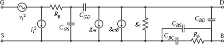
FIGURE 8.2 Equivalent input noise generator MOS small signal model. (Reprinted from Noulis, T., Siskos, S. and Sarrabayrouse, G., IET Circuits Dev. Syst., 2, 324–334, 2008. With permission.)
In addition to the channel thermal and the flicker noise, MOS transistors also exhibit parasitic noise due to the resistive polygate and substrate resistance. These parasitic noise sources in modern semiconductor technologies should be taken into account, since the polygate resistance Rg and substrate resistance Rb depend mainly on the layout structure of MOS transistors, and the related modeling is quite advanced; also, by using specific layout techniques their noise contribution can be minimized. However, these noise sources are critical in high-frequency applications and can be considered negligible in the case of the detector readout integrated circuits (ICs).
The respective equivalent simplified input noise MOSFET model is shown in Figure 8.2 [18].
This model is based on the fact that the noise performance of any two-port network can be represented by two equivalent noise generators at the input stage of the network [19]. The two equivalent input noise generators are calculated from Figure 8.2 and are shown by Equations 8.4 and 8.5:
(8.4) |
(8.5) |
Since the factor (gm/2πCGD) is much higher than the transistor cutoff frequency fT, the term jωCGD can be neglected with respect to gm for all practical cases of interest. It is also essential to note that these two terms of Equations 8.4 and 8.5 are fully correlated.
High-density semiconductor front-end systems are designed according to low-noise criteria. The noise performance of a detector readout system is generally expressed as the equivalent noise charge (enc) and is defined as the ratio of the total rms noise at the output of the pulse shaper to the signal amplitude due to one electron charge q. The noise contribution of the amplification stage is the dominant source that determines the overall system noise and should, therefore, be optimized. The main noise contributor of the analog part is the CSA input MOSFET, and the noise types associated with this device are 1/f and channel thermal noise [12].
The total noise power spectrum at the CSA output due to the thermal and flicker noise sources is given by Equation 8.6 [9,10]:
(8.6) |
where:
Ct = the total CSA input capacitance
υeq = the total equivalent noise voltage of the input MOS transistor
The total integrated rms noise is given by Equation 8.7:
(8.7) |
where H(jω) is the transfer function consisting of a semi-Gaussian shaper pulse shaper. The encs due to thermal and 1/f noise, considering Equations 8.4,8.5,8.6,8.7 and for an amplifier with capacitive source, are given by Equations 8.8 and 8.9 [9,10]:
(8.8) |
(8.9) |
where:
B = the beta function [9]
q = the electronic charge
τs = the peaking time of the shaper
n = the order of the semi-Gaussian shaper
Capacitances Cd, Cf, CGS, and CGD are capacitances of detector, feedback, gate-source, and gate-drain of the input MOSFET, respectively, and Cp is the parasitic capacitance of the interconnection between the detector and the amplifier input, which in this application is considered as negligible. The total input stage capacitance is given by Equation 8.10 [9,18,20,21]:
(8.10) |
Input MOSFET optimum gatewidths exist for which the respective thermal and flicker encs are minimal. These optimum dimensions are extracted by minimizing the respective encs of Equations 8.8 and 8.9, respectively [9]. The optimal gatewidths are given in Equations 8.11 and 8.12:
(8.11) |
(8.12) |
where α is defined as α=1+(9Xj)/(4L) and Xj is the metallurgical junction depth. Equations 8.11 and 8.12 are valid when capacitance Cd is in the picofarad range.
It can easily be determined which noise component (thermal or 1/f) dominates, by calculating whether the ratio of the respective equivalent noise charges is above or below unity. The noise comparison ratio (NCR) depends also on the technology, comes from Equations 8.6 and 8.7, and is given by Equation 8.13 [20]:
(8.13) |
When it is known, for a given technology and for a MOSFET operating in the saturation regime, which noise component, thermal or 1/f, dominates, the type and optimum dimensions of the preamplifier input MOSFET can be selected, considering that typically p-channel transistors have less 1/f noise than their n-channel counterparts, since their majority carriers (holes) are less likely to be trapped due to their lower mobility [18].
It is obvious that CSA input noise is in practice defined by the detector capacitance, the peaking time specification, and the selection of the input MOS type and dimensions (as previously analyzed). A large detector capacitance results in a higher input noise, as it affects the input node biasing. Additionally, the thermal and flicker equivalent noise voltages (encs) are proportional to Ct, whose value is mainly affected by Cd. The peaking time specification determines the operating bandwidth of the readout system. Consequently, it determines the flicker or thermal noise dominance, since the 1/f noise is negligible in the frequency region after 10 kHz. Concerning Equations 8.11 and 8.12, these formulas are the result of the optimization methodology, and they are used in calculating NCR (Equation 8.13). The dimensions of the input MOSFET are also selected according to these equations (W1/f if it is a p-channel MOSFET [PMOS] or Wth if it is an n-channel MOSFET [NMOS]) [18].
8.3.1 CHARGE-SENSITIVE AMPLIFIER DESIGN
The CSA (Figure 8.3) is commonly implemented using a folded cascode structure, built of transistors M1, M2, and M4 [21,22]. This architecture provides a high direct current (dc) gain and a relatively large operating bandwidth. The folded cascode amplifier has an n-channel input transistor (or drive), but a p-channel transistor is used for the cascode (or common-gate) transistor. A complementary structure can also be configured, always in relation to the noise specs of the application (melecom). This configuration allows the dc level of the output signal to be the same as the dc level of the input signal [22,23]. If the circuit is designed to operate with dc coupling detectors, CSA should be able to supply a current in the range from a few picoamperes up to a few nanoamperes through the feedback loop in order to match the detector leakage current. The open-loop gain of such a configuration is determined by the ratio of currents in the left and the right branch of the folded cascode, the sizes of the input transistor and the load transistor, and the total current Id1 in the input transistor [21,22].
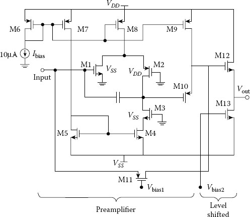
FIGURE 8.3 Charge-sensitive preamplifier using a folded cascode amplifier. (Reprinted from Noulis, T., Siskos, S., Sarrabayrouse, G. and Bary, L., Circuits and systems I: Regular papers, IEEE Trans. Circuits Syst. Part 1, 55, 1858 © (2008) IEEE. With permission.)
Regarding the CSA reset mechanism, the integrated reset device provides a continuous discharge of the feedback capacitance and a dc path for the detector leakage current and defines the dc operating point of the amplifier. A simple resistor would not be a feasible reset device. In fact, in order to make its thermal noise negligible compared with the shot noise associated with the leakage current, its value should not be relatively high (e.g., a 500 MΩ resistor introduces an amount of thermal noise equal to the shot noise of 100 pA leakage current) and cannot be integrated on a small silicon area. An active device (MOS or bipolar) should be used instead [24]. The CSA reset device was configured with a PMOS transistor (M11) biased in the triode region in order to avoid the use of a high-value resistance (Figure 8.3).
Transistors M9 and M10 implement an output buffer for the CSA circuit. The current mirror architecture of transistors M6, M7, and M8 is biasing using the Ibias current source. The feedback capacitance Cf is placed between the CSA input node and the gate of the source follower transistor configuration stage for stability reasons. This feedback capacitance Cf is discharged via the input node, which is connected to both Cf and transistor M11. Transistor M3 is in cascade configuration with M4, the MOSFET comprising the current mirror M5, and was placed in the CSA in order to achieve higher output resistance.
In the specific design, the maximum signal swing must be limited for keeping all the devices in the saturation regime, that is, VGS > VT and VDS > VGS–VT. Therefore, the bias current source Ibias has been selected with a specific low value in order to achieve a low power dissipation performance.
The simplified small signal equivalent circuit of the core folded cascode amplifier without the feedback capacitance, the reset device, and transistor M3, which is in cascade configuration with M4, are shown in Figure 8.4.
The open-loop gain AV = (V0/Vi) is given by Equation 8.14 [18]:
(8.14) |
where:
(8.15) |
(8.16) |
(8.17) |
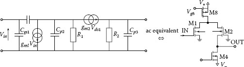
FIGURE 8.4 Small signal equivalent circuit of the open-loop preamplifier. (Reprinted from Noulis, T., Siskos, S., and Sarrabayrouse, G., IET Circuits Dev. Syst., 2, 324–334, 2008. With permission.)
(8.18) |
(8.19) |
The DC gain AV0 of the two-port network is given in Equation 8.20:
(8.20) |
and the dominant pole is
(8.21) |
The PMOS-based equivalent resistor operating as a reset device has a value of
(8.22) |
where I is the drain current.
Using the specific reset device implementation, the equivalent resistor can be externally modified by suitably fixing the gate bias voltage of the PMOS-based equivalent resistor. However, since the gate bias voltage is conditioned by the other parameters (the power consumption specification, the process and its allowable supply voltages, the charge–discharge time specification, etc.), the dimensions of the feedback MOS are also suitably selected according to each application [18].
Considering the noise analysis of the folded cascode structure, in Figure 8.5 the basic structure of the folded cascode amplifier (in relation to our preamplifier configuration) is depicted, including all the equivalent MOSFET noise-current sources.
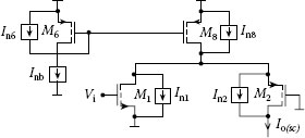
FIGURE 8.5 Folded cascode amplifier equivalent schema structure with noise current sources. (Reprinted from Noulis, T., Siskos, S., and Sarrabayrouse, G., IET Circuits Dev. Syst, 2, 324–334, 2008. With permission.)
The total noise current is equal to (Equation 8.23) [18]
(8.23) |
Performing the approximations (r06//g−1 m6) ≌ g−1 m6 and (r01//r08//r02//gm2−1), the equivalent noise voltage is given by Equation 8.24:
(8.24) |
The respective square value is
(8.25) |
While noise contribution is theoretically generated by M6, M8, and the dc bias current source, in practice their contribution can be neglected when reflected to the amplifier topology input. As is shown by Equations 8.1,8.2,8.3,8.4,8.5, the generated noise current of each MOS transistor separately is dependent on its drain current. Specifically, the equations show that low-noise performance in a MOSFET requires a large value of transconductance (gm, which, in turn, means that the transistor should have a large W/L ratio and be operated at a high quiescent current level. In practice, as drain current increases, noise performance decreases and power consumption increases. As is obvious from the preamplifier circuit, the current flowing through M8 (which in practice is obtained by the current source and the respective current mirror structure) is “shared” in M1 and M2 of the folded cascode amplifier. Taking into consideration the large dimensions of M1, its noise contribution is the dominant noise source of the CSA, and therefore the noise methodology is focused on its noise optimization. Therefore, the full noise-optimization methodology is focused on the input node conditions and consequently on the input transistor type and dimensions. Other design parameters that can be optimized in terms of noise performance are the peaking time and the order of the shaper, always in relation to the radiation-detection application specifications.
8.3.2 SEMI-GAUSSIAN SHAPING FILTER DESIGN
Semi-Gaussian (S-G) pulse-shaping filters are the most common pulse shapers employed in readout systems. Their use in electronics spectrometry instruments is to measure the energy of charged particles [25], and their purpose is to provide a voltage pulse whose height is proportional to the energy of the detected particle. The theory behind pulse-shaping systems, as well as different realization schemes, can be found in the literature [25,26]. It has been proved that a Gaussian-shaped step response provides optimum signal-to-noise characteristics. However, the ideal S-G shaper is noncasual and cannot be implemented in a physical system. A well-known technique to approximate a delayed Gaussian waveform is to use a CR-RCn filter [25]. The principle of such a shaper is schematically shown in Figure 8.6.
A high-pass filter (HPF) sets the duration of the pulse by introducing a decay time constant. The low-pass filter (LPF), which follows, increases the rise time to limit the noise bandwidth. Although pulse shapers are often more sophisticated and complicated, the CR-RCn shaper contains the essential features of all pulse shapers, a lower frequency bound and an upper frequency bound, and it is basically an (n + 1) order band pass filter (BPF), where n is the number of integrators. The transfer function of an S-G pulse shaper consisting of one CR differentiator and n RC integrators (Figure 8.6) is given by Equation 8.26 [9,10]:

FIGURE 8.6 Principle diagram of a CR-(RC)n shaping filter: (a) with RC HPF; (b) with RL HPF.
(8.26) |
where:
τd = time constant of the differentiator
τi = time constant of the integrators
A = integrators’ dc gain
The number n of the integrators is called shaper order. Peaking time is the time when the shaper output signal reaches peak amplitude and is defined by
(8.27) |
Increasing the value of n results in a step response, which is closer to an ideal Gaussian but with larger delay. The order n and peaking time τs, depending on the application, may or may not be predefined by the design specifications.
The operating bandwidth of an S-G shaper is given by
(8.28) |
The above combined band-pass frequency behavior enhances the signal-to-noise ratio by separating the “noise sea” from the signal’s main Fourier components. The choice of cutoff frequencies defines the shaper’s noise performance and consequently the signal-to-noise ratio. In addition, the frequency domain transfer characteristics are strictly linked to shaper time domain behavior or output pulse shape [20]. Pulse shaping has two conflicting objectives. The first is to restrict the bandwidth to match the measurement time. The second is to constrain the pulse so that successive signal pulses can be measured without undershoot or overlap (pileup). Reducing the pulse duration increases the allowable signal rate, but at the expense of electronic noise. In designing the shaper, these conflicting goals should be balanced. Many different considerations lead to the “nontextbook” compromise that optimum shaping depends on the application [27].
Concerning shaper peaking time, in order to achieve a value predefined from the application specifications, the shaper model’s passive elements should be suitably selected.
The total CSA–second-order S-G shaper system transfer function using a Laplace representation is
(8.29) |
where:
Apr = the preamplifier gain
τpr = its time rise constant
Considering as input signal a Dirac pulse δ(t), by taking the inverse Laplace transform of the product, the output signal in the time domain is given by Equation 8.30 [21,28,29]:
(8.30) |
Solving the above integral, the output signal of the readout system is
(8.31) |
where k1, k2, k3, and k4 are the following constants (Equations 8.32,8.33,8.34,8.35) [21,28,29]:
(8.32) |
(8.33) |
(8.34) |
(8.35) |
Using the above equations, the values of all the shaper model’s passive elements are selected.
8.3.2.1 Operational Transconductance Amplifier (OTA)-Based Shaper Approach
The main problem in the design of very-large-scale integration (VLSI) shaping filters for nuclear spectroscopy is the implementation of long shaping times, in the order of microseconds, for which high-value resistors (in the megaohm range), capacitors (in the 100 pF range), or both are demanded. In fact, the practical values in terms of occupied area that can be integrated are in the range of tens of kiloohms for the resistors and in the picofarad range for the capacitors.
Few examples of monolithic shaping structures providing long shaping times can be found in the literature. In all the above topologies, different techniques are used in order to obtain relatively large peaking times within a reasonable occupied area. Specifically, Chase et al. have suggested [30] the use of demultiplying current mirrors to increase the resistor value responsible for setting the filtering time constant of the op-amp-based low-pass filter. De Geronimo et al. have also proposed [31] a versatile architecture using current mirrors to magnify the resistances and still based on voltage-mode op-amps as gain blocks. Finally, Bertuccio et al. [32] adopted a current-mode approach to design a first-order low-pass filter, avoiding the use of operational amplifiers, that results in a very compact topology.
In this chapter, an alternative design technique is described, and an IC semi-Gaussian shaping structure is suggested. The proposed topology, in contrast to the typical shaping structures, is not based on op-amps, which generally demand large-area input transistors and high bias currents, but on operational transconductance amplifiers (OTAs). Extended study of all available OTA-based configurations, in both voltage and current domains, was performed by Noulis et al. [28,29]. All possible implantations were investigated using all the available advanced filterdesign techniques.
Also in this chapter, a leapfrog OTA-based architecture is described [21]. Although its operating bandwidth is in the low-frequency region, it is fully integrated and is characterized by low power and low noise performance compatible with the stringent requirements of high-resolution nuclear spectroscopy. However, the main advantage of the specific shaper design is its continuous time-adjustable operating bandwidth, which renders it suitable for a variety of readout applications.
In particular, with respect to Figure 8.6, a two-port passive-element network was designed in order to implement an equivalent fully integrated second-order semi-Gaussian shaping filter. This two-port passive network is shown in Figure 8.7 [21].
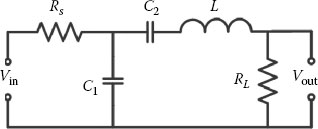
FIGURE 8.7 Equivalent RLC minimum-inductance two-port circuit of a second-order S-G shaper.
The specific passive-element topology has a respective transfer function (Laplace representation) to the typical shaper model. Its Laplace representation transfer function for a second-order S-G shaper is given by Equation 8.36 [21]:
(8.36) |
From the above two-port network, the signal flow graph (SFG) of a second-order S-G shaping filter is extracted (Figure 8.8).
The output signal of the passive network, in relation to the above SFG, is
(8.37) |
Using the extracted SFG and the leapfrog (functional simulation method) design methodology, a second-order shaper is designed. The main advantage of the leapfrog method over other filter design methods, which also provide integrated structures, is the better sensitivity performance and the capability to optimize the dynamic range by properly intervening during the phase of the original passive synthesis [33,34]. In order to implement the shaping filter, operational transconductance amplifiers (OTAs) were selected as the basic building cells. A diagram of an OTA is shown in Figure 8.9.
The OTA is assumed to be an ideal voltage-controlled current source and can be described by
(8.38) |
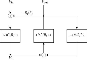
FIGURE 8.8 Signal flow graph of a voltage-mode second-order semi-Gaussian shaper.

FIGURE 8.9 Diagram of OTA.
where:
I0 |
= |
output current |
V + and V- |
= |
noninverting and inverting input voltages of the OTA, respectively |
Note that gm (transconductance gain) is a function of the bias current, IA. The implementation of the S-G shaping filter with OTAs is highly advantageous, since it provides programmable characteristics. In particular, tunability is achieved by replacing the RC and CR sections in the original passive model with active gm-C sections, where the gm can be adjusted with an external bias voltage or current. The second-order shaping filter that was designed using the above SFG and the leapfrog method is shown in Figure 8.10.
The capacitor values and OTA transconductances of the above S-G shaper are given in Table 8.1. The shaper configuration was designed in order to provide a peaking time equal to 1.8 μs, which refers to a bandwidth of 260 kHz in the low-frequency region (fc1 = 140 Hz). The passive element values of the respective RLC-equivalent two-port network of Figure 8.7 are also given in Table 8.1.
Because of the nonintegrable value of C2 in the leapfrog shaper, the specific capacitance was substituted with a grounded OTA-C capacitor simulator. The respective OTA architecture is described in Figure 8.11, and its calculated value is given by Equation 8.39 [33,34]. The values of the transconductances and the capacitor C are gm4=gm5=gm6=74.4 μA/V, gm7=950 nA/V, and C = 12.8 pF.

FIGURE 8.10 OTA-based second-order S-G shaper using the leapfrog technique.
TABLE 8.1
IC Shaper and RLC Equivalent Network Element Values
IC Shaper |
RLC Network |
|||
Actives and Passives |
Passives |
|||
gm1 |
24 μA/V |
RS |
100 Kω |
|
gm2 |
11.5 μA/V |
RL |
100 Kω |
|
gm3 |
950 nA/V |
C1 |
10.3 Pf |
|
C1 |
13 pF |
C2 |
7.4 nF |
|
C2 |
1.00 nF |
L |
84 mH |
|
C3 |
14 pF |
|||
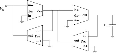
FIGURE 8.11 OTA-based architecture for grounded capacitance simulation. (Reprinted from Noulis, T., Siskos, S., Sarrabayrouse, G. and Bary, L., Circuits and systems I: Regular papers, IEEE Trans. Circuits Syst. Part 1, 55, 1857 © (2008) IEEE. With permission.)
(8.39) |
8.3.3 ADVANCED CSA-SHAPER ANALOG SIGNAL PROCESSOR IMPLEMENTATION
Using the analysis and methodology presented in Sections 8.2.1 and 8.2.2 on the CSA and shaper design, respectively, an advanced fully integrated radiation-detection analog processing channel was designed and fabricated [29]. The preamplifier–shaper readout front-end system was designed, simulated, and fabricated in a 0.35 μm CMOS process (3M/2P 3.3/5V) by Austria Mikro Systeme (AMS, Unterpremstätten, Austria) for a specific low-energy x-ray silicon strip detector.
The design specifications are given in Table 8.2 [18,21] and Table 8.3 [18,21].
TABLE 8.2
Design Specifications
Detector Diode PIN (Si) |
|
Detector capacitance |
Cd = 2–10 pF |
Leakage current |
Ileak = 10 pA |
Charge Q collected per event |
Q = 312.5 ke− |
Time t needed for the collection of the 90% of the total charge Q |
300 ns |
Preamplifier–Shaper |
|
Shaper’s order |
n = 2 |
Shaper peaking time value |
τs = nτ0 = 1.8 μs |
Temperature value |
25°C |
Power consumption per processing channel |
Less than 8 mW |
TABLE 8.3
CSA-Level Shifter MOS Transistor Dimensions
MOS Transistors |
(W/L) (μm) |
M1 |
310/0.9 |
M2 |
100/0.7 |
M3 |
25/1.5 |
M4, M5 |
2.5/5 |
M6, M7, M9 |
2.5/2.5 |
M8 |
5/2.5 |
M10 |
100/0.7 |
M11 |
20/1 |
M12, M13 |
5/5 |
Source: Noulis, T., Deradonis, C., Siskos, S., VLSI Design J., 2007, 71684, 2007.
The preamplifier was designed using the architecture provided in Figure 8.3. Related extended analysis of the design methodology is available in Section 8.2.1. The transistor dimensions and the biases for this configuration were selected according to the design and optimization criteria presented in Section 8.2.1 The transistor dimensions are provided in Tables 8.2 and 8.3, and the biases are provided in this section. The level shifting stage was added as the dc bias level of the signal provided to the shaper to be controlled and the general dynamic range and 1 dB compression point of the filter to be optimized. The feedback capacitance Cf is 550 fF, and it is placed between the input node and the gate of the source follower stage to avoid introduction on the closed loop of the follower stage complex poles and to isolate the Cf from the following stage. The bias current Ibias was selected to be 10 μA. The power supplies are VDD = −VSS = 1.65 V, and the reset device bias voltage is fixed to 150 mV. The level shifting bias voltage is equal to −1.18 V [29].
The shaper was implemented with the leapfrog architecture and OTA-based grounded capacitance simulator replacement structure, depicted in Figures 8.10 and 8.11. An inherent drawback of the leapfrog methodology, and consequently of the particular shaper architecture, is that the leapfrog design method provides a gain value of 1/2 [33,34]. In order to cope with this specific loss, an additional gain stage was used after the preamplifier and before the shaper, using an OTA-based structure (gm8 = 153 μA/V, gm9 = 11.5 μA/V) provided in Figure 8.12.
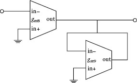
FIGURE 8.12 OTA-based amplification stage. (Reprinted from Noulis, T., Siskos, S., Sarrabayrouse, G. and Bary, L., Circuits and systems I: Regular papers, IEEE Trans. Circuits Syst. Part 1, 55, 1859 © (2008) IEEE. With permission.)
The specific topology gives the capability to program the gain externally by fixing the bias voltage of the two OTA components. In particular, the dc gain of the above OTA structure is A = Vout/Vin = gm8/gm9. Considering the S-G OTA-based shaping architecture, capacitor simulator, and amplification topology of Figures 8.10, 8.11, and 8.12, respectively, they were implemented using the CMOS OTA configuration, shown in Figure 8.13.
In the transconductance circuit, a typical CMOS cascode configuration is used, where changing the bias voltage results in approximately equal changes for both the transconductance and the 3 dB frequency. The MOS dimensions of all the OTA circuits are given in Table 8.4.
The PMOS devices in the OTA circuits have their bulk biased in the same voltage to their source (designing separate wells), taking advantage of the specific n-well CMOS process that is used, in order to avoid the body effect and to maximize the signal swing. The power supplies in all the OTA components are also VDD = −VSS = 1.65 V. The bias voltage of each OTA is fixed at −0.85 V in order to achieve the desired transconductance values. The total simplified block diagram of the analog readout ASIC is given in Figure 8.14.
The fabricated chip in which the prototype x-ray readout ASIC was implanted is shown in Figure 8.15. The measured x-ray IC front-end system output signal is shown in Figure 8.16. The system provides dc gain equal to 120 dB. However, as will be presented below, this value can be externally modified by suitably fixing the bias voltages and consequently changing the gm values of the OTA-based amplification topology of Figure 8.12. Regarding the radiation-detection application specifications, the output pulse has a peaking time value of 1.81 μs that shows no undershoot or pileup.
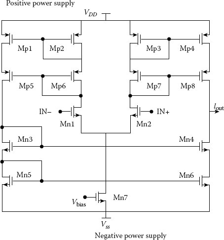
FIGURE 8.13 CMOS operational transconductance amplifier.
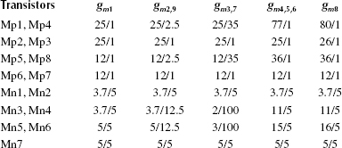
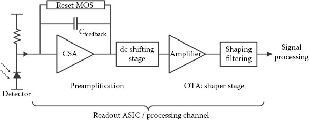
FIGURE 8.14 Block diagram of the IC readout system.
FIGURE 8.15 Microphotograph of the full fabricated microchip (the readout system is circled). (Reprinted from Noulis, T., Siskos, S., Sarrabayrouse, G. and Bary, L., Circuits and systems I: Regular papers, IEEE Trans. Circuits Syst. Part 1, 55, 1860 © (2008) IEEE. With permission.)
The power consumption is 1 mW, far lower than the maximum allowable specified value of 8 mW, rendering the system low power [24,35].
The readout ASIC noise performance was also analytically studied. The system enc is 382 e− for a detector of 2 pF, and noise performance increases with a slope of 21 e−/pF. The enc dependence on the detector capacitance variations is shown in Figure 8.17.
The linearity of the front-end system energy resolution is presented in Figure 8.18. The CMOS readout analog processor achieves an input charge gain–voltage output conversion of 3.31 mV/fC and a linearity of 0.69%.
In terms of the total occupied area, the specific IC system is again advantageous, since it consumes only 0.2017 mm2 of a total 2.983 × 2.983 mm2 microchip [36,37].

FIGURE 8.16 Readout system output pulse. (Reprinted from Noulis, T., Siskos, S., Sarrabayrouse, G. and Bary, L., Circuits and systems I: Regular papers, IEEE Trans. Circuits Syst. Part 1, 55, 1860 © (2008) IEEE. With permission.)

FIGURE 8.17 Readout ASIC enc dependence on detector capacitance. (Reprinted from Noulis, T., Siskos, S., Sarrabayrouse, G. and Bary, L., Circuits and systems I: Regular papers, IEEE Trans. Circuits Syst. Part 1, 55, 1860 © (2008) IEEE. With permission.)
Finally, the flexibility of the system for use in a wide range of readout applications taking advantage of the specific shaping stage topology was examined. The system gain is programmable from 118 to 137 dB by changing the OTAs’ bias voltage of the gain stage. This gain programmability is demonstrated in Figure 8.19. Furthermore, the peaking time can be similarly externally modified. This is represented in Figure 8.20, in which output signals with peaking times from 1 to 3 μs are provided by suitably fixing the bias voltages of the OTA configurations, which operate in the total shaper architecture as integrators and the OTAs in the capacitance simulator unit. As the peaking time increases, the shaper upper frequency becomes higher in its band-pass response. This particular OTA-based S-G shaper provides continuously variable peaking time in the range from 950 ns to 3.1 μs. A variation of about 30% in signal amplitude can be detected when moving from the shortest to the longest available peaking time. The output signal undershoot can also be externally adjusted. In Figure 8.21, different output signal undershoots are shown. The undershoot can vary from 0% to 18% of the positive signal amplitude. This results in a respective increment of the low 3 dB frequency, providing a narrower shaper bandwidth. Consequently, the output noise can also be regulated in relation to each application. Regarding the system, and particularly the S-G shaping filter stability, having only one feedback between its input and output, no stability problems were observed. In addition, no sensitivity problems occurred in relation to the gm terms, since their value could be fixed externally using the respective bias voltages.
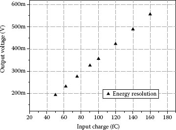
FIGURE 8.18 Readout ASIC measured energy response. (Reprinted from Noulis, T., Siskos, S., Sarrabayrouse, G. and Bary, L., Circuits and systems I: Regular papers, IEEE Trans. Circuits Syst. Part 1, 55, 1860 © (2008) IEEE. With permission.)

FIGURE 8.19 Gain programmability. (Reprinted from Noulis, T., Siskos, S., Sarrabayrouse, G. and Bary, L., Circuits and systems I: Regular papers, IEEE Trans. Circuits Syst. Part 1, 55, 1861 © (2008) IEEE. With permission.)
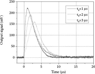
FIGURE 8.20 Adjustable peaking time capability: output signal for different peaking times. (Reprinted from Noulis, T., Siskos, S., Sarrabayrouse, G. and Bary, L., Circuits and systems I: Regular papers, IEEE Trans. Circuits Syst. Part 1, 55, 1861 © (2008) IEEE. With permission.)
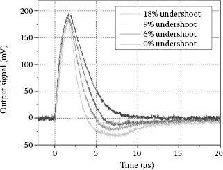
FIGURE 8.21 Variable output signal undershoot capability: different output signal undershoot. (Reprinted from Noulis, T., Siskos, S., Sarrabayrouse, G. and Bary, L., Circuits and systems I: Regular papers, IEEE Trans. Circuits Syst. Part 1, 55, 1861 © (2008) IEEE. With permission.)
8.4 CURRENT CHALLENGES AND LIMITATIONS
Radiation-detection IC design imposes new challenges and limitations as the technology nodes are shrinking.
In terms of the technology used, CMOS has scaled down to 28 and 20 nm, allowing extremely dense integration and cost minimization for high-volume production. However, in terms of noise optimization, performance, and cost, the process selection should always be defined by the related application. While the noise is becoming lower in submicron technologies, extra noise sources should be taken into account, such as gate-induced noise and channel-reflected noise. In terms of circuit design, advanced noise-optimization methodologies are needed at the level of both circuit architecture and mask design (physical layout), as these noise contributors need to be optimized. While in previous technology nodes these were almost negligible, now, at 28 nm and below, these may contribute up to 50% of the noise, depending always on the application and mostly on the operating circuit/system frequency bandwidth.
In addition, the related transistor noise models, always in relation to the used technology Foundry, are not always adequate to provide an accurate simulation, and the related performance cannot be effectively optimized. Advanced models are needed for the designer to be able to access the trade-offs and to optimize the radiation-detection IC processor.
Furthermore, in terms of radiation hardness, extreme limitations exist. Models for pre- and postradiation conditions are needed, as the performance needs to be accessed in real operation mode. No technology foundry provides this kind of simulation support, and as a result the related performance degradation after irradiation cannot be estimated effectively in all the presilicon design stages and verification. Advanced modeling techniques are required, and device layouts for radiation-hard operation are demanded for the integrated circuits to be able to cover the operation specifications in an irradiated environment. This is a gap in the design flow that constantly renders radiation IC design extremely risky.
1. E. Beuville, K. Borer, E. Chesi, E. H. M. Heijne, P. Jarron, B. Lisowski and S. Singh, Amplex, a low-noise, low-power analog CMOS signal processor for multi-element silicon particle detectors, Nuclear Instruments and Methods in Physics Research Section A 288(1) (1990) 157–167.
2. L. T. Wurtz and W. P. Wheless Jr., Design of a high performance low noise charge preamplifier, IEEE Transactions on Circuits and Systems I 40(8) (1993) 541–545.
3. S. Tedja, J. Van der Spiegel and H. H. Williams, A CMOS low-noise and low-power charge sampling integrated circuit for capacitive detector/sensor interfaces, IEEE Journal of Solid State Circuits 30(2) (1995) 110–119.
4. Radeka, V., Rehak, P., Rescia, S., Gatti, E., Longoni, A., Sampietro, M., Holl, P., Struder, L. and Kemmer, J. Design of a charge sensitive preamplifier on high resistivity silicon, IEEE Transactions on Nuclear Science 35(1) (1988) 155–159.
5. Radeka, V., Rehak, P., Rescia, S., Gatti, E., Longoni, A., Sampietro, M., Bertuccio, G., Holl, P., Struder, L. and Kemmer, J. Implanted silicon JFET on completely depleted high-resistivity devices, IEEE Electron Device Letters 10(2) (1989) 91–94.
6. Lund, J. C., Olschner, E., Bennett, P. and Rehn, L. Epitaxial n-channel JFETs integrated on high resistivity silicon for x-ray detectors, IEEE Transactions on Nuclear Science 42(4) (1995) 820–823.
7. Lechner, P., Eckbauer, S., Hartmann, R., Krisch, S., Hauff, D., Richter, R., Soltau, H., et al. Silicon drift detectors for high resolution room temperature x-ray spectroscopy, Nuclear Instruments and Methods in Physics Research Section A 377 (1996) 346–351.
8. Ratti, L., Manghisoni, M., Re, V. and Speziali, V. Integrated front-end electronics in a detector compatible process: Source-follower and charge-sensitive preamplifier configurations, In: James, R. B. ed., Hard X-Ray and Gamma-Ray Detector Physics, III Proceedings of SPIE 4507 (2001) 141–151.
9. Sansen, W. and Chang, Z. Y. Limits of low noise performance of detector readout front ends in CMOS technology, IEEE Transactions on Circuits and Systems 37(11) (1990) 1375–1382.
10. Chang, Z. Y. and Sansen, W. Effect of 1/f noise on the resolution of CMOS analog readout systems for microstrip and pixel detectors, Nuclear Instruments and Methods in Physics Research Section A 305 (1991) 553–560.
11. Steyaert, M., Chang, Z. Y. and Sansen, W. Low-noise monolithic amplifier design: Bipolar versus CMOS, Analog Integrated Circuits and Signal Processing 1(1) (1991) 9–19.
12. Motchenbacher, C. D. and Connelly, J. A. Low-noise Electronic System Design (Wiley Interscience, New York, 1998).
13. Xie, D., Cheng, M. and Forbes, L. SPICE models for flicker noise in n-MOSFETs from subthreshold to strong inversion, IEEE Transactions on Computer-Aided Design 19(11) (2000) 1293–1303.
14. Noulis, T., Siskos, S. and Sarrabayrouse, G. Comparison between BSIM4.X and HSPICE flicker noise models in NMOS and PMOS transistors in all operating regions, Microelectronics Reliability 47 (2007) 1222–1227.
15. Jakobson, C. G., Bloom, I. and Nemirovsky, Y. 1/f noise in CMOS transistors for analog applications from subthreshold to saturation, Solid-State Electronics 42(10) (1998) 1807–1817.
16. Nemirovsky, Y., Brouk, I. and Jakobson, C. G. 1/f noise in CMOS transistors for analog applications, IEEE Transactions on Electron Devices 48(5) (2001) 921–927.
17. Liu, W. MOSFET Models for SPICE Simulation including BSIM3V3 and BSIM4 (Wiley, New York, 2001).
18. Noulis, T., Siskos, S. and Sarrabayrouse, G. Noise optimized charge sensitive CMOS amplifier for capacitive radiation detectors, IET Circuits, Devices & Systems 2(3) (2008) 324–334.
19. Chang, Z. Y. and Sansen, W. Low Noise Wide Band Amplifiers in Bipolar and CMOS Technologies (Kluwer, Norwell, MA, 1991).
20. Noulis, T., Deradonis, C., Siskos, S. and Sarrabayrouse, G., Programmable OTA based CMOS shaping amplifier for x-ray spectroscopy, Proceedings of 2nd IEEE PRIME (Otranto, Lecce, Italy, 2006).
21. Noulis, T., Siskos, S., Sarrabayrouse, G. and Bary, L. Advanced low noise X-ray readout ASIC for radiation sensor interfaces. IEEE Transactions on Circuits and Systems Part 1, 55(7) (2008) 1854–1862.
22. Vandenbussche, J., Leyn, F., Van der Plas, G., Gielen, G. and Sansen, W. A fully integrated low-power CMOS particle detector front-end for space applications, IEEE Transactions on Nuclear Science 45(4) (1998) 2272–2278.
23. Guazzoni, C., Samprieto, M. and Fazzi, A. Detector embedded device for continuous reset of charge amplifiers: Choice between bipolar and MOS transistor, Nuclear Instruments and Methods in Physics Research Section A 443 (2000) 447–450.
24. Pedrali-Noy, M., Gruber, G., Krieger, B., Mandelli, E., Meddeler, G., Moses, W. and Rosso, V. PETRIC-A position emission tomography readout integrated circuit, IEEE Transactions on Nuclear Science 48(3) (2001) 479–484.
25. Konrad, M. Detector pulse-shaping for high resolution spectroscopy, IEEE Transactions on Nuclear Science 15(1) (1968) 268–282.
26. Ohkawa, S., Yoshizawa, M. and Husimi, K. Direct synthesis of the Gaussian filter for nuclear pulse amplifiers, Nuclear Instruments and Methods in Physics Research Section A 138(1) (1976) 85–92.
27. Goulding, F. S. and Landis, D. A. Signal processing for semiconductor detectors, IEEE Transactions on Nuclear Science 29(3) (1982) 1125–1141.
28. Noulis, T., Deradonis, C., Siskos, S. and Sarrabayrouse, G. Detailed study of particle detectors OTA based CMOS semi-Gaussian shapers, Nuclear Instruments and Methods in Physics Research Section A 583 (2007) 469–478.
29. Noulis, T., Deradonis, C. and Siskos, S. Advanced readout system IC current mode semi-Gaussian shapers using CCIIs and OTAs, VLSI Design Journal 2007 (2007) 71684.
30. Chase, R. L., Hrisoho, A. and Richer, J. P. 8-channel CMOS preamplifier and shaper with adjustable peaking time and automatic pole-zero cancellation, Nuclear Instruments and Methods in Physics Research Section A 409 (1998) 328–331.
31. De Geronimo, G., O’Connor, P. and Grosholz, J. A generation of CMOS readout ASIC’s for CZT detectors, IEEE Transactions on Nuclear Science 47 (2000) 1857–1867.
32. Bertuccio, G., Gallina, P. and Sampietro, M. ‘R-lens filter’: An (RC)n current-mode lowpass filter, Electronics Letters 35 (1999) 1209–1210.
33. Deliyannis, T., Sun, Y. and Fidler, K. Continuous-Time Active Filter Design (CRC Press, Boca Raton, FL, 1999).
34. Sedra, A. S. and Brackett, P. O. Filter Theory and Design: Active and Passive (Pitman, London, 1979).
35. Krieger, B., Ewell, K., Ludewigth, B. A., Maier, M. R., Markovic, D., Milgrome, O. and Wang, Y. J. An 8 × 8 pixel IC for x-ray spectroscopy, IEEE Transactions on Nuclear Science 48(3) (2001) 493–498.
36. Limousin, O., Gevin, O., Lugiez, F., Chipaux, R., Delagnes, E., Dirks, B. and Horeau, B. IDeF-X ASIC for Cd(Zn)Te spectro-imaging systems, IEEE Transactions on Nuclear Science 52(5) (2005) 1595–1602.
37. Shani, G. Electronics for Radiation Measurements, vol. 1. (CRC Press, Boca Raton, FL, 1996), pp. 182–183.