
Silicon Photomultipliers for High-Performance Scintillation Crystal Read-Out Applications |
CONTENTS
15.2 A Short History of The SiPM
15.3.1 Geiger-Mode Avalanche Photodiode
15.3.2 Silicon Photomultiplier
15.3.4 SiPM Operation in Detail
15.4.1 Photon Detection Efficiency
15.6.2 Clear Micro Leadframe Package
15.7.1 Issues of SiPM Reliability Assessment
15.7.2 Reliability Assessment of SiPMs
15.8 Scintillation Crystal Readout
15.8.2 Energy Resolution and Coincidence Timing Measurements
15.8.3 SiPM Scintillation Crystal Performance
15.8.4 Coincidence Resolving Time
Silicon photomultipliers (SiPMs) have emerged as the solid-state alternative to the vacuum tube photomultiplier tube (PMT) in a number of scintillation detection applications ranging from medical imaging to radiation detection and isotope identification. The primary technical and commercial driver for the development of the SiPM has been medical imaging, specifically positron emission tomography (PET). There is a simultaneous requirement in PET for higher-quality images and a lower raw component sensor cost compared with the PMT. The radiation detection market requires higher-performance sensors for better isotope identification, increased physical robustness for handheld and field operations, low operating voltage compared with the high voltage of the PMT, and reduced sensor cost for high-volume homeland security applications. A typical generic application example of an SiPM detecting the light emission from a scintillating crystal is shown in Figure 15.1. This figure shows the scintillation crystal coupled to an SiPM sensor that is directly connected to a printed circuit board (PCB). The signal from the SiPM is typically processed via an amplifier or shaper or both, followed by data acquisition. The scintillation crystal is capable of converting the incident gamma rays to visible photons and the SiPM sensor has the sensitivity to convert the visible photons to electrical charge, which can be amplified, shaped, and read out by the electronics. The SiPM is typically mounted on a PCB and due to its compact nature it is possible to place the read-out electronics on the same PCB.
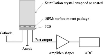
FIGURE 15.1 Simplified diagram of a detector and read-out block diagram for scintillation crystal readout.
The SiPM can be used to replace the PIN photodiode, the avalanche photodiode (APD), or the PMT currently used in these systems. For all applications the main benefits of SiPM technology include: high optical sensitivity, low operating voltage, unsurpassed uniformity across the sensor, uniformity from sensor to sensor, small form factor, and low cost. Specifically, the sensors discussed in this chapter will be complementary metal–oxide–semiconductor (CMOS)-manufactured SiPM sensors, which have been developed to meet the performance and cost requirements of medical imaging PET and radiation detection markets.
15.2 A SHORT HISTORY OF THE SiPM
The SiPM sensor, now in mass-production, has been developed through knowledge of the Geiger-mode operation of photodiodes, which can be traced back to the original work of Haitz [1,2,3,4] and Oldham et al. [5]. The Geiger-mode photodiode was used as a tool to investigate diode breakdown properties and microplasmas in diodes and it helped to develop the diode impact ionization and avalanche breakdown models. The work of McIntyre [6,7] developed equations allowing for a full understanding of the device physics in a practical and workable model of breakdown and above breakdown Geiger-mode operation. Further published work on Geiger-mode technology during the 1980s and 1990s centered on using the Geiger-mode photodiode for single-photon counting applications [8]. This work was largely focused on individual photodiode sensors with external quenching circuitry [9,10]. In the late 1990s and early 2000s, the SiPM concept emerged from Russia through work published by Saveliev [11], Bisello [12], and Golovin [13]. However, the development of the SiPM concept can be traced back to papers published in the 1970s by Krachenko et al. [14,15] in which arrays of Geiger-mode avalanche sensors, passively quenched, were used for low-light sensing. At the time of publication in 1978, the authors noted a limitation of PN photodiodes as an avalanche-based sensor in the presence of microplasmas in the photodiode depletion region, which limits the useful size of the photodiode’s active area. This limitation was removed in the late 1990s and 2000s, as Geiger-mode photodiodes were developed utilizing higher-quality start material and processing conditions and architectures were developed that reduced the presence of defects in the depletion region of the photodiode. This advance allowed large Geiger-mode photodiode arrays to be fabricated. These developments allowed the SiPM to be manufactured in CMOS foundries, creating a cost-competitive alternative to the PMT.
In this section, the SiPM will be described in more detail, from the basic theory of operation to the major parameters that govern sensor performance. The basic theory of the SiPM will be developed from the theory of Geiger-mode operation of single microcells, to arrays of microcells that form the model for the SiPM.
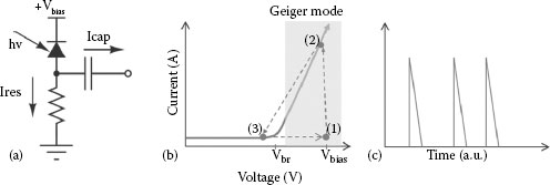
FIGURE 15.2 (a–c) Basic schematic and operation of a Geiger-mode avalanche photodiode.
15.3.1 GEIGER-MODE AVALANCHE PHOTODIODE
The basic building block of an SiPM is a photodiode that is sensitive to single photons, possesses high internal gain, and self regulates its output current. A circuit schematic of the basic structure that accomplishes this is shown in Figure 15.2a. The photodiode in Figure 15.2a is designed to operate in Geiger mode so that it can detect single photons. The resistor in series with the photodiode provides the means of limiting the current flow and resetting the photodiode after each photon is detected. Geiger-mode operation can be explained by reviewing the current versus voltage characteristic shown in Figure 15.2b. This figure shows the ideal reverse bias characteristics for a photodiode and overlays the mode of operation, known as Geiger mode, which allows for single-photon detection. A photodiode has a breakdown voltage (Vbr) at which point the current flow in the diode significantly increases. For operation in Geiger mode, a voltage in excess of Vbr is applied (Vbias), as shown in Figure 15.2b. The difference in voltage between Vbias and Vbr is termed the overvoltage and typical values are between 1 and 5 V. Initially, on application of Vbias, no current flows in the photosensitive region of the photodiode. There is always a small parasitic current, shown in Figure 15.2b, flowing in the photodiode, which to the first order can be neglected. On arrival of a photon and conversion of the photon into an electron–hole pair, the charge carriers undergo impact ionization, leading to avalanche multiplication. During the avalanche process, the photodiode current changes from a no current state, labeled as (1) in Figure 15.2b, to a high current state, labeled as (2). The current generated in the photodiode follows two paths in Figure 15.2a, shown as Ires and Icap. Once Ires begins to flow through the photodiode, the voltage is dropped across the series resistor. The voltage drop causes the photodiode voltage and the electric field to decrease and the operating point shown in Figure 15.2b moves from (2) to (3). As a current is no longer flowing across the resistor, the voltage bias across the photodiode increases to the original Vbias and the photodiode returns to a state that can detect the next photon. The output from this type of sensor is shown in Figure 15.2c and can be used to explain both Ires and Icap.* The output current is characterized by a sharp and fast rise time at the onset of the incident photon, relating to the transition from (1) to (2) and a slower recovery time as the photodiode transitions from (3) back to (1). As will be shown in subsequent sections, the addition of a capacitor to the photodiode and resistor provides a simple means of accessing the fast switching behavior inside the SiPM.
The output signal from the Geiger-mode APD consists of nearly identical current pulses in time. Each current pulse relates directly to the detection of a photon or thermal noise event in the sensor. The thermal noise, known as the dark count rate, has the same properties as a single photon and will be shown to be a key parameter for the understanding of SiPM operation.
15.3.2 SILICON PHOTOMULTIPLIER
The Geiger-mode APD provides single-photon sensitivity and it outputs a current pulse that signals the arrival time of the incident photon. However, the Geiger-mode APD is a binary sensor and does not have the ability to sense multiple-photon events since the output can be considered identical regardless of the photon number. Additionally, the size of the photodiode is limited by two effects: firstly, the characteristic dark count noise increases with the active area; and secondly, the recovery time (during which the sensor is insensitive to further incident photons) increases with the increasing capacitance of the diode, which in turn increases with the active area. Therefore, only relatively small Geiger-mode APDs are used, typically tens to hundreds of micrometers in diameter. To allow for both a large-area sensor and to detect multiple photons, the SiPM was created. The structure of the SiPM is shown in Figure 15.3a. A key feature of the SiPM architecture is the large array of parallel-connected Geigermode APDs with quenching elements and output capacitors* connected together. Each photodiode, resistor, and capacitor element is collectively called the microcell. The schematic in Figure 15.3a shows a simplified SiPM demonstrated as a 4 × 3 array of microcells. A commercial SiPM would have from hundreds to thousands of microcells per millimeter squared. The SiPM is biased with a positive voltage on the cathode with respect to the anode. The SiPM output can be measured as the current flow from the cathode to the anode, or from the fast output. A representation of the output of an SiPM in response to a low-level light pulse is shown in Figure 15.3b. This image was captured on an oscilloscope with the persistence setting set to allow for displaying multiple detected events. To create the voltage signal, the output of the SiPM was connected to an external resistive load.

FIGURE 15.3 (a) Silicon photomultiplier schematic. (b) Characteristic output response of a SiPM as viewed on an oscilloscope with the persistence setting engaged.
Figure 15.3b shows several key features of the SiPM output, such as (1) the ability to detect multiple-photon events; (2) the dark count signal, which is at the same level as the single photoelectron signal; and (3) cross talk, which is an unwanted feature caused by cotriggering inside the SiPM. The detection of multiple photons is shown as the clearly discernible voltage levels labeled 1–5 phe. These represent the detection of between 1 and 5 single photons. The photon number detection is a desired characteristic while the dark count and cross talk are negative features of the SiPM operation. Reviewing the architecture in Figure 15.3a, it is clear that in an SiPM there is an optically active photodiode as well as optically inactive structures such as the resistor and capacitor. The necessity to provide a physical separation for the individual microcell photodiode elements required for independent Geiger-mode operation means that there is a dead space between photodiodes, which limits the total active area. The percentage of active area in an SiPM is termed the fill factor and must be considered with the number of microcells that are in each SiPM. A higher fill factor increases photon detection efficiency (PDE) at the expense of the dynamic range. The different aspects of this issue will be covered in more detail in subsequent sections.
The SiPM has three outputs, as shown in Figure 15.3a. The connection for biasing the photodiode is made through the cathode and anode terminals. In this example, the anode is directly connected to the quenching resistor. However, this is still termed the anode since it assists the user in the application of the correct bias voltage for reverse bias operation. The additional fast output is shown as a capacitively coupled output, which is directly connected to the microcell at the intersection between the anode and the quench resistor. The output signal is shown in Figure 15.4 for a fastpulsed laser with a pulse width of less than 100 ps. The anode–cathode output is characterized by a fast onset time followed by the recovery of the output signal, which is governed by the internal impedance of the SiPM and the external circuitry directly connected to the sensor. The recovery time increases with the photodiode area and the quench resistor and parasitic impedance. The fastest recovery times are achieved with the smallest microcell size, but at the expense of the fill factor. The fast output signal is characterized as a short fast pulse, which is the derivative of the switching behavior of the photodiode during Geiger-mode operation detailed in Figure 15.2b (1 and 2). The decay time, which is a feature of the anode–cathode signal, is not present; instead, this is replaced by a small undershoot to the baseline voltage as the microcell recovers. The fast output accurately represents the signal and since the recovery time is removed from the output signal it is easier to identify additional incident photons within the recovery period. It will be shown that scintillation crystal readout can be achieved with excellent energy and coincidence timing resolution using only the signal from the fast output.
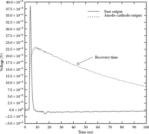
FIGURE 15.4 Pulse output a from 3 × 3 mm2 SiPM with 35 μm microcells. Fast output and anode–cathode output are shown superimposed on the same graph.
15.3.4 SIPM OPERATION IN DETAIL
Sections 3.1, 3.2 and 3.3 described the basic operation of the SiPM. In this section, the theory of operation will be reviewed in more detail. As has been shown, the SiPM provides the ability to detect individual photons and provides an output current that is proportional to the number of incident photons. This is a key factor for the read out of the light emission from a scintillation crystal, as discussed in Section 15.8.1. For the SiPM to be able to detect the photons emitted from scintillation crystals and output current pulses as shown in Figure 15.3b and Figure 15.4, the following processes must occur:
1. Photon capture: The photon must be absorbed and converted into an electron–hole pair.
2. Amplification: The electron–hole pair must be converted to a measurable current through the internal gain mechanism of the SiPM.
Photons entering the SiPM are absorbed according to the Beer–Lambert equation for photon absorption given as
(15.1) |
where:
I0 |
= |
incident photon flux (typically photons per second) |
α(λ) |
= |
attenuation coefficient of silicon at the wavelength of interest |
z |
= |
distance into the SiPM |
This equation determines the ability of an SiPM to detect photons of a given wavelength. Using the scintillator peak emission values given in Figure 15.5 and combining these with the attenuation coefficients for crystalline silicon [16], it is possible to calculate the percentage of photons absorbed as a function of the distance into the SiPM. This calculation is shown in Figure 15.6 for various peak intensities of scintillators relevant to this work. LaBr3 [17] emits photons with a peak wavelength at 380 nm and Figure 15.6 shows that almost 100% of these photons are absorbed at a distance of 0.2 μm into the SiPM. Conversely, at 0.2 μm only 10% of the photons from CsI(Tl), which has an emission peak at 550 nm, are absorbed.

FIGURE 15.5 Crystal emission light yield from common scintillation crystals used in radiation detection.
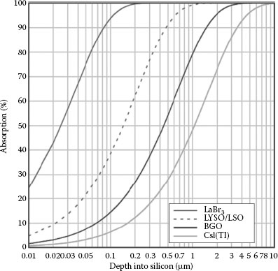
FIGURE 15.6 Photon absorption in SiPM sensors for various crystal peak emission wavelengths.
A longer emission wavelength requires an increased depletion region width to allow the efficient capture of the incident photons. However, all the scintillators described here emit photons in a range that can be sensed by SiPM devices, which possess shallow junctions on the order of 0.2–1 μm, and are the subject of this work. These SiPM rely on the planar, shallow structures that CMOS processing is ideally suited to fabricate.
Once a photon has been absorbed by the SiPM, the next step is the amplification of the generated electrons and holes. This amplification is governed by the impact ionization of electrons and holes in the depletion region of the photodiode. The depletion region of a P-on-N photodiode, shown in Figure 15.7a, is the region of high electric field established where the N-type and P-type doped silicon layers come together. This dopant structure is fully compliant with standard CMOS processing, which is used for the production of high-quality SiPMs in volume. The anode of the photodiode for a P-on-N structure is located close to the surface beneath an antireflection coating (ARC), which has been designed to maximize photon transmission into the silicon. The cathode of the photodiode is below the anode and is electrically connected to a low-resistance substrate of the same dopant type. To put the physical sizes in perspective, a typical silicon wafer that is used to manufacture an SiPM is on the order of 750 μm thick while the depletion region with a breakdown voltage of 24.5 V is on the order of 1 μm thick. Most of the active volume of the SiPM that is designed for radiation detection is located close to the surface and the substrate typically provides a low ohmic contact to the cathode and necessary structural support.
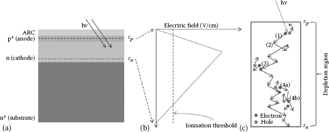
FIGURE 15.7 (See color insert) (a) Simplified cross section of a P-on-N Geiger-mode APD structure. (b) Electric field profile across the photodiode depletion region. (c) A pictorial representation of an avalanche breakdown in a photodiode across the depletion region.
The SiPM avalanche process is governed by the electric field across the depletion region of the photodiode as shown in Figure 15.7b. With knowledge of the cathode and anode dopant levels, Poisson’s equation can be used for the calculation of the electric field across the junction. For the discussion here, it is sufficient to know that the depletion region electric field is increased through the application of a reverse bias voltage. When a reverse bias is applied to the SiPM in excess of the breakdown voltage, the electric field increases beyond the ionization threshold. At this point, charge carriers gain sufficient energy to create further electron–hole pairs through collisions, a process called impact ionization. If the electric field is sufficiently high then avalanche breakdown will occur. Avalanche breakdown is pictorially represented in Figure 15.7c as a succession of charge-carrier movements labeled (1) through (4). As the charge carrier passes through the depletion region, it is accelerated by the electric field. The electric field accelerates electrons toward the cathode and holes toward the anode. The acceleration increases the carrier kinetic energy but carriers cannot pass through the depletion region without interacting with the underlying silicon structure. Two main types of interactions can occur: phonon generation or impact ionization. Phonon generation is shown as (1) and (2) in Figure 15.7c and results in a scattering event that reduces the kinetic energy of the charge carrier. Ionization events are shown as (3), (4a), and (4b) in Figure 15.7c. The ionization causes the generation of additional electron–hole pairs, which can themselves generate ionization events, as shown in (4b). With a sufficiently high electric field, the impact ionization process can, in theory, continue indefinitely. However, with the inclusion of the quench resistor in the microcell, as shown in Figure 15.2a, the electric charge at each breakdown event, and therefore the current, is limited to only the capacitance of the microcell’s photodiode. The avalanche process provides the output current and the characteristic breakdown voltage of the SiPM.
It is important to discuss the major sensor parameters that impact the performance characteristics of the SiPM. The following are considered the basic SiPM sensor parameters:
• Breakdown voltage: the voltage at which the SiPM current increases rapidly with increasing reverse bias
• Photon detection efficiency (PDE): the absolute PDE of the SiPM including all geometrical effects
• Dark count: the number of false single pulse height signals measured per second
• Gain: the internal gain of the SiPM in response to a single photon
• Cross talk: the output signal caused by one microcell randomly firing one or more additional microcells in the array
• Afterpulsing: the secondary avalanche events that are triggered by stored charge during a previous event
• Dynamic range: the ability of an SiPM to detect incoming photons without saturation
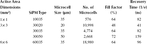
To aid in the understanding of the sensor parameters discussed, Table 15.1 is used. This details the various SiPM types available, including the active area, the microcell size, the number of microcells, and the fill factor. It is important to note that the microcell size used in this table is the size of the active area of the microcell and not the pitch of the microcells in the SiPM. These parameters are from the current commercial SiPM produced by SensL [18].
Each of these parameters will impact the radiation detection performance when the SiPM is coupled to a scintillating crystal. The individual parameters are discussed next, including information on their accurate measurement.
15.4.1 PHOTON DETECTION EFFICIENCY
The PDE is a key parameter for SiPM operation. This parameter determines the percentage of photons that will be detected by an SiPM. The PDE of an SiPM can be defined by the following equation:
(15.2) |
where:
QE(λ) = internal quantum efficiency of the SiPM
AIP = avalanche initiation probability
FF = fill factor of the SiPM
The QE is wavelength dependent and includes any losses at the optical interface of the sensor. The AIP is set by the doping levels and the physics of the depletion region of the photodiode and increases with voltage. The FF is a geometrical parameter that is governed by the ratio of the active area to the nonactive area in the SiPM microcell.
To measure the PDE, an accurate measurement must be made that utilizes photon statistics. In photon statistics that are inherent in SiPM sensors there is a specific relationship between the ratio of events that trigger zero photons, N0, and the total number of events that include any total number of photons, Ntot. This relationship is determined through the chance of observing a zero photon event in a Poisson probability distribution with a mean number of photons, nph, and can be written as To correctly take account of background pulses, a measurement in the dark must be obtained. The parameters and must be measured, and then the mean number of photons, nph, arriving at the SiPM can be calculated using
(15.3) |
The PDE can then be calculated by dividing the mean rate of detected photons by the recorded rate of arriving photons, given by the optical power recorded by a calibrated photodiode P and the period T of the light pulses:
(15.4) |
Here, R is the geometrical optical power ratio between the light falling on the SPM and the calibrated photodiode. An example of this measurement technique that is extensively referenced is the work of Eckert [19]. This technique produces the true SiPM PDE that does not contain the effects of cross talk or afterpulsing.
Figure 15.8 shows the PDE for a 30035 type SiPM across the wavelength range of 250–1100 nm. The peak emission is shown at 420 nm with a maximum peak detection efficiency of 41% achieved at 5.0 V overvoltage.

FIGURE 15.8 Photon detection efficiency versus wavelength for a 30035 SiPM at overvoltages of 2.5 and 5.0 V.
The PDE varies with the microcell size according to the fill factor for the different types of SiPM. The PDE does not vary with the active area dimension. Therefore, the fill factor values listed in Table 15.1 can be used to scale the PDE shown in Figure 15.8 to different sensors. To scale the PDE to different sensor types, first divide the PDE of the known SiPM by the fill factor of the known SiPM and then multiply by the fill factor of the unknown SiPM. As an example, to scale the 5.0 overvoltage PDE at 420 nm from the 30035 to the 30050 SiPM the following equation would be used: 41%/0.64 * 0.72 = 46%.
The dark count rate is defined as the pulse rate measured in the dark, with a leading-edge trigger at 0.5 times the single photoelectron amplitude. The single photoelectron amplitude is determined by observing when the count rate first decreases as the leading-edge threshold is increased. By increasing the threshold until the dark rate changes, it is possible to determine the maximum pulse height of the single photoelectron counts. A measurement of the dark count rate is not impacted by cross talk but can be influenced by afterpulsing. In Section 15.4.5, afterpulsing will be shown to be very low for the SiPM sensors discussed here and not a significant factor in the measured dark count rate. The dark count rate for 10035, 30035, and 60035 SiPM is shown versus overvoltage in Figure 15.9. This demonstrates a very well-controlled dark count rate versus an overvoltage that is suitable for mass-production applications that require SiPM sensor output stability over a wide range of overvoltage conditions and across a wide range of temperatures.

FIGURE 15.9 Measurement of dark count rates for 10035, 30035, and 60035 SiPMs.
For scintillators with a short decay time, the dark count rate can be largely ignored. For example, Table 15.4 shows that LaBr3 has a decay time constant of 16 ns and typically pulses are integrated on the order of 100 ns to achieve good energy resolution and full signal collection. For a 100 ns signal integration time using a 60035 sensor, and using the dark count values as shown in Figure 15.9, the average number of dark counts integrated can be calculated as 5 × 107* 100 × 10−9 = 5. The dark count rate is clearly not a dominant factor for an LaBr3 which emits ~63 photons per kiloelectron volt and therefore would emit more than 40,000 visible photons in response to a single 662 keV gamma ray. For scintillators with longer characteristic decay times such as CsI(Tl), combined with the desire to detect low-energy gamma rays in the tens of kiloelectron volts, the dark count rate becomes a more important factor. The dark count rate can degrade the signal-to-noise ratio. Advances in SiPM production are leading to improved dark count rates. An example of next-generation dark count rates for SiPMs is shown in Figure 15.10 compared with the existing family of SiPMs. This shows the achievement of a dark count rate of less than 100 kHz/mm2.

FIGURE 15.10 Dark count rate of next-generation SiPMs. Dark count rates are based on 35 μm-based microcell sensors representing dark count rates per millimeter square for 10035, 30035, and 60035 sensors.
The gain of an SiPM is defined as the mean number of charge carriers generated when a single charge initiates an avalanche process in the depletion region of the sensor. This is a unitless parameter and determines the amount of charge flowing through the sensor during detection. The gain can be derived theoretically using the following equation:
(15.5) |
where:
Cmicrocell = capacitance of a single microcell
Vbias = operating voltage
Vbr = breakdown voltage
q = electronic charge
Knowledge of the gain of the SiPM aids in the conversion between the dark count rate and the measured dark current in the SiPM by the following equation:
(15.6) |
where:
DCR = dark count rate in hertz
G = gain
CT = cross-talk probability
AP = afterpulse probability
It is possible to approximate the SiPM by ignoring the CT and AP terms if they are deemed sufficiently small. This is appropriate for first-order calculations but cross talk and afterpulsing should always be considered for the most accurate estimations.
To measure the gain of an SiPM requires knowledge of the current flowing through the sensor measured while in saturation using a pulsed light source. A standard pulsed light-emitting diode (LED) of 470 nm can be used for the measurement. The basic concept of the measurement is as follows: if all microcells of an SIPM are illuminated simultaneously and with a known repetition rate, it is possible to infer the gain of the sensor by measuring the DC current flowing through the standard anode–cathode. Once this is obtained, it is necessary to subtract the dark current, Idark, from the photocurrent, Iphoto. The gain is then
(15.7) |
where:
q = electron charge
flaser = laser pulse frequency
N = number of microcells
The gain measurement completed in this way does not contain afterpulsing or cross talk and is a true representation of the gain of an SiPM. A plot of the gain for the different SiPM microcell types is shown in Figure 15.11. No difference was noted between samples of different active area type that utilize the same microcell structure.
The gain values for the fast output terminals were designed to be between 2% and 4% of the standard anode–cathode gain and were set so that the gain was not dependent on the microcell size. A measured gain for the fast output was therefore found to be 4.3 × 10⁴ regardless of microcell type at 2.5 V overvoltage. The gain measurement technique was also used to accurately determine the temperature coefficient of the breakdown voltage. The point of the zero crossing gain versus the voltage curve was measured at a range of temperatures. The breakdown voltage was found to vary by 21.5 mV/°C over standard operating temperature ranges.
A cross-talk event can be seen in the output signal of an SiPM, as shown in Figure 15.3b. Cross talk is defined as the ratio of the pulse rate measured at 1.5 times the single photoelectron amplitude to 0.5 times the single photoelectron amplitude. Cross talk is an undesirable phenomenon, in that a single-firing microcell fires one or more neighboring microcells almost instantaneously. Crosstalk pulses can therefore appear as multiple output signals in response to a single photon, and are therefore a form of multiplication noise impacting the excess noise factor. Increasing the bias voltage increases cross talk. Cross talk can be caused by electrical charge leakage or it can be optically generated due to the emission of light in SiPM sensors.
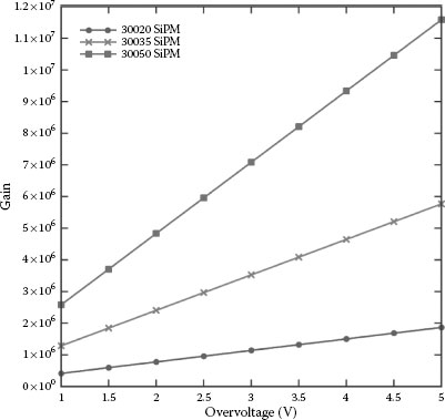
FIGURE 15.11 Gain measurement for the standard anode–cathode output for B-series 30020, 30035, and 30050 SiPMs.
To measure the cross talk in SiPM sensors, the rate of dark counts as a function of an increasing leading-edge trigger threshold is measured, and is repeated at various bias voltages. An example of the output from this type of measurement is shown in Figure 15.12. The y-axis indicates the frequency of the dark count measured for the input trigger threshold on the x-axis.
As shown in Figure 15.12, this results in a staircase dependence of rate versus trigger threshold, and progresses to lower rates as the trigger threshold increases. The 1.5 (height) and 0.5 (height) photoelectron rates can then be measured and the ratio computed for each overvoltage. Using this procedure, the cross talk measured for 30020, 30035, and 30050 SiPMs is shown in Figure 15.13.
Cross talk was not seen to depend on the size of the individual die and has been found to only depend on the size of the microcells. To investigate this phenomenon, the cross talk on 10035 and 60035 SiPMs was measured. The cross talk on these SiPMs was within measurement accuracy for the 30035 SiPM and can be considered identical regardless of the die size. For the 30020 sensors, the cross-talk rates were found to be extremely low and difficult to measure without long measurement cycle times. The measurements below 2 V overvoltage were in fact terminated due to the length of time that it was taking for the measurement. These 10020 SiPM exhibit cross talk of sub 6% at the 5.0 V level. In all cases, the cross talk at typical operating overvoltages for the SiPM reported in this work were found to be extremely low. It is expected that for most applications, the 30035 will provide the best combination of low cross talk and high PDE.
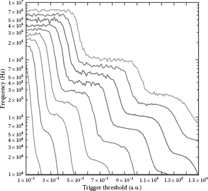
FIGURE 15.12 Cross-talk threshold plot for a 30035 SiPM. Data are taken from 1 to 5 V overvoltage.
Afterpulsing is the phenomenon of an SiPM microcell randomly discharging with higher probability shortly after a previous discharge than at the expected thermal generation rate. Afterpulse events that occur after the recovery time cannot be distinguished from genuine, photon-induced events and therefore deteriorate the photon-counting resolution of an SiPM. Typical timescales for this phenomenon are tens of nanoseconds, comparable with the microcell recovery time. As a result, many afterpulse events are of partial discharge compared with the single photoelectron discharge of a microcell, due to partial recharge of the microcell.

FIGURE 15.13 Measurement of cross talk for 30020, 30035, and 30050 SiPMs.
Afterpulsing is an undesirable effect because it increases the variance of the single cell charge, reduces the dynamic range, and increases cross talk in the SiPM. The degree of afterpulsing depends on the bias voltage, the temperature, the design of the deep doping implant, and the recovery time.
Afterpulse probability measurements are made by binning the time between consecutive pulses and extracting via the formula:
(15.8) |
where:
(15.9) |
(15.10) |
where:
ntp |
= |
thermal rate probability density |
nap |
= |
afterpulse probability rate, consisting of fast and (optionally) slow components |
ξ |
= |
charge fraction of a second pulse time Δt after a given pulse |
Afterpulsing was not found to be dependent on the SiPM die size but only on the microcell geometry. The afterpulse rates measured for 30020, 30035, and 30050 SiPMs are shown in Figure 15.14.
The results obtained for 10035 and 60035 SiPMs were within measurement error to the 30035 SiPM. This demonstrates the low level of afterpulsing present in the SiPM, and for the 30020 and 30035, afterpulse rates are less than or equal to 5% up to 5.0 V overvoltage. The afterpulsing measured on the 30050 was found to be similar to the 30035 until 4.5 V. After 4.5 V, the afterpulsing of the 30050 increased more rapidly than the 30035. It was believed that the high gain of the 30050, as shown in Figure 15.11, was the cause for the increase in afterpulsing at overvoltages in excess of 4.5 V. The low level of afterpulsing in the SiPM presented demonstrates the high quality of the start material and processing steps used to fabricate these SiPM sensors.

FIGURE 15.14 Afterpulse measurements on 30020, 30035, and 30050 SiPMs.
The dynamic range of the SiPM is determined by the number of microcells over the active area that are available to detect incoming photons. For fast scintillation decay time crystals, such as LaBr3 and LYSO (Table 15.4), the decay time is shorter than the decay time of a typical SiPM (Table 15.1) and to the first order the crystal emission can be considered as a pulse source. For longer decay crystals such as CsI(Tl) this becomes more complicated as microcells can recover and respond multiple times during a scintillation emission. For simplicity, only the pulse dynamic range will be considered here. To the first order, the dynamic range of the SiPM can be considered simply by the following equation:
(15.11) |
where:
M = number of microcells per die
PDE = photon detection efficiency at a specified lambda
Nph = number of incident photons
A characteristic curve can be plotted for this equation using basic information derived from the datasheet of SiPM products. For Figure 15.15, the dynamic range for a pulsed light is shown from the single photon level up to 107 photons. For each die type, the parameters of M and PDE have been obtained from the datasheet for the B-Series SiPM [18].
Taking the photon yield of a scintillator such as LYSO from Figure 15.5 as 32 photons per kiloelectron volt, and assuming an incident gamma-ray photon of 511 keV, approximately 16,352 visible photons should be emitted. Assuming a 50% loss from the light collection and transfer to the SiPM and a PDE of 41% at the peak wavelength of 420 nm from Figure 15.8, there should theoretically be ~3352 photons incident on the sensor. From Figure 15.15 it can be seen that with this number of photons incident on the sensor it would generate a signal equivalent to ~700 microcells firing. Additionally, this signal level is at the top end of the linear range of the sensor. For this reason, the 30035 sensor type with 35 microcells works well with LYSO crystals though careful analysis of the linearity should be performed to produce the most accurate energy resolution measurements.
The uniformity of the sensor operating parameters is important for using SiPM sensors in high-volume applications. The sensor uniformity minimizes the variation between sensors and reduces or eliminates voltage adjustment between sensors that are used in a system. To demonstrate uniformity, this section will review end-of-line test data obtained during the manufacturing of SiPMs. The sensors described in this section are from SensL’s B-Series sensors. These sensors are manufactured on 200 mm wafers in a CMOS foundry, typically in lots of 25 wafers. On completion of the fabrication process, each wafer is comprehensively tested, first in a wafer acceptance test (WAT) using a process control monitor (PCM), and then at component probe (CP) using a product test. The WAT verifies that the wafer was processed correctly and that key technological parameters such as the breakdown voltage and diffused and deposited film resistances are on target and within specified test limits. These test limits were established based on technology target values, material and process characteristics such as film thickness and resistivities, and from data collected during the technology development phase from skew or split lots. The measurement data from WAT are monitored wafer to wafer and lot to lot and trends are analyzed to verify process capability and stability. This process is a standard part of SensL’s B-series manufacture and is repeated for all commercial SiPM sensors produced.
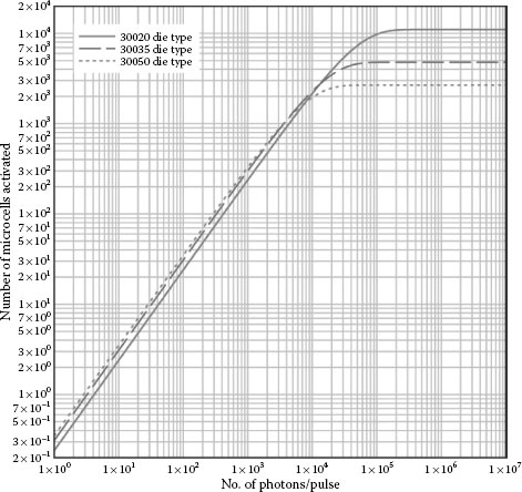
FIGURE 15.15 Dynamic range calculations for 30020 (10998 microcells), 30035 (4774 microcells), and 30050 (2668 microcells) die types.
Following the PCM test, all SiPMs are tested at CP using tester hardware that has been developed for SiPM sensor testing. For B-Series SiPM sensors, the breakdown voltage, dark current, and optical response to short wavelength light are critical parameters that are measured on the SiPM product die. SensL has established a wafer probe flow that measures every die on the wafer under dark and illuminated conditions with appropriate optical filters, so that the response of the SiPM sensor under broadband and short wavelength conditions is measured. Die with failing characteristics are identified on electronic wafer maps, and only those die that pass all of the quality and performance screens are subsequently assembled as packaged sensors. Further details of the key parameters that are measured at CP are provided in the following sections.
The breakdown voltage is defined as the value of the voltage intercept of a parabolic line fit to the current versus the voltage curve, and in the CP wafer test flow this parameter is calculated from measurements of the dark current at several bias points. Figure 15.16 shows the distribution of the breakdown voltage values as measured from several production lots obtained during the qualification of a single die-size product. For the breakdown voltage variation plot shown here, a total sample size of ~204,000 SiPM sensors of the 30035 type was included. A mean breakdown voltage of 24.69 V was measured. The measured values are seen to be tightly distributed with a standard deviation of 73 mV, and all die have breakdown voltage values within ±0.25 V of the mean.

FIGURE 15.16 Histogram of the breakdown voltage distribution for a 30035 SiPM. Data are from ~204,000 commercial sensors.
The uniformity of the breakdown voltage is believed to be due to the tight process control and design of the SensL SiPM. Similar data were obtained for the 60035 SiPM at the wafer level.
Dark current is a key parameter for the SiPM, and is measured in the CP flow at several bias points below and above the breakdown voltage. Die with dark currents that are outside specification are screened out and inked electronically so that they are not assembled into a package. Figure 15.17 shows the tight distribution of dark current values for the 30035 SiPM. For Figure 15.17 all SiPMs were measured at an overvoltage equal to 2.5 V.
Figure 15.17 shows the tight distribution of the SiPM dark current and is within product specification. Additional work is currently under way to reduce the dark count for future SiPM sensors through process improvements.
To ensure the quality of the SiPM, the output current from the sensor die is measured in the CP flow under tightly controlled illumination conditions at a number of overvoltages. For the measurements shown here, all SiPMs were measured at a fixed constant voltage of 29.5 V with a uniform and calibrated blue light source. The output current measurement allows an integrated assessment of the sensor gain and PDE. Any variation in gain or PDE has the potential to impact the optical current. By measuring all die on the wafer, it is possible to develop a full understanding of the optical uniformity of the SiPM. Figure 15.18 shows the distribution of output current values as measured from several production lots, with a total sample size of approximately 142,000 for the SiPM sensor of the 30035 type. This measurement procedure was only established during the latter portion of this work and therefore the size of the data set is smaller than the data set that represented the breakdown voltage and dark current measurements.
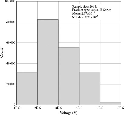
FIGURE 15.17 Histogram of dark current data from a 30035 SiPM. The sample size is ~204,000 and all SiPMs were measured at an overvoltage equal to 2.5 V.
In a high-volume application it is desirable to be able to operate all of the SiPMs in a system at the same voltage. The use of a fixed voltage in this test, as opposed to a fixed overvoltage, fully demonstrates the uniformity of the SiPMs. By measuring with a fixed voltage, the effect of breakdown voltage variations from die to die, wafer to wafer, and lot to lot was included and variations in parameters such as film thickness, doping level, and gain were integrated into the final result shown. The measured distribution illustrates the tightly controlled uniformity characteristics of the B-Series SiPM manufacturing flow, with uniformity in the range ±10% for optical currents at these bias conditions.
While the uniformity of the SiPM sensors has been shown to be extremely good, it is useful to investigate the major cause of the uniformity variation in commercial SiPM. This can be accomplished by plotting the breakdown voltage of each SiPM from a wafer lot to the optical uniformity that was measured at 29.5 V. This is shown in Figure 15.19 for over 50 k die from a single wafer lot. The die type is 30035 and all data are plotted in the figure. This shows a correlation coefficient of 0.87 to a linear fit of the data indicating a strong link between the breakdown voltage and the optical uniformity measured. This demonstrates the advantages of tight process control on the final uniformity that can be achieved using SiPMs manufactured in this manner.
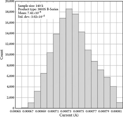
FIGURE 15.18 Optical uniformity at a constant voltage equal to 29.5 V.
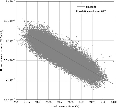
FIGURE 15.19 Correlation plot generated from wafer-level data showing illumination current at 29.5 V against the measured breakdown voltage from over 50k 30035 type SiPMs.
The packaging of the sensor plays a large role in the overall performance of the system and one that is not often considered in assessing sensor performance. Multiple factors such as wavelength, allowable operating temperature range, soldering conditions, and reliability vary depending on the package type and construction. In this section, the main types of packaging used for SiPMs that are suitable for radiation detectors will be described. A key criterion for many radiation detectors is the need for a large-area optical sensor to read out a large scintillator or a large scintillator array. This necessitates packages that have the ability to be closely tiled together to form large-area sensors with single readouts or sensor arrays with multiple SiPM readouts. The package types discussed in this section are all suitable for use in large-area arrays and can be pixelated or summed as required by the user.
There are three major packaging types that are suitable for use with scintillation crystals in a radiation detector. These package types are:
1. Poured epoxy-coated die in a ceramic or laminate carrier
2. Clear micro leadframe package (MLP)
3. Wafer-scale packaging through silicon via (TSV)
Each of these package types has positive and negative aspects, which should be understood during a product design process. To assist in understanding the variations between packages, the following criteria are critical to understand and can be used to evaluate package suitability for an application. The criteria used to decide on a package type are:
1. Array fill factor: The ratio of the optically active area to the peripheral area. The fill factor is important when creating arrays of SiPMs, which are typically available in 1, 3, and 6 mm2 sizes. This parameter is not critical if a single sensor can be used alone in a detector. For applications requiring large-area coverage, a high package fill factor is critical to capture as many incident photons coming from the scintillation crystal.
2. Optical transmission: The transmission characteristics of a package vary depending on the package type chosen. Compounding this problem is that the optical transmission can be wavelength dependent. As shown in Section 15.8.1, the peak emission wavelength varies between crystal types. Therefore, it is important to make sure that the package does not limit the light collection from the scintillation material.
3. Operating conditions: The temperature that a package can physically operate in depends on the package construction and material.
4. Reliability: The various package types used for sensors have different failure mechanisms, which lead to different inherent reliability.
5. Service life: The service life or wear out time of the sensor will be determined primarily by the degradation in transmissivity of the package material.
6. Uniformity and reproducibility: The uniformity of the package surface is important to maintain optimum crystal coupling to an SiPM. The reproducibility of the package is important so that consistent results can be obtained in large-area array applications.
7. Cost: The cost of a package must be understood and is important for highvolume applications. Low cost is obviously desirable if the performance and operating-life criteria can be met.
The following subsections will review each of the three main package types with respect to the criteria that have been outlined here.
This category covers a broad range of packaged parts that all use poured epoxy as the covering layer over the SiPM. The epoxy layer provides protection to the SiPM surface and prevents damage to wire bonds. For large-area arrays, the fabrication process entails attaching multiple die to a ceramic or PCB carrier using die attach epoxy. Following die attach and cure, the contact pads on the SiPM are wire bonded to the substrate. For the creation of scalable large-area arrays with uniform performance and wiring track-out, only packages in which the wire bonds are connected directly to the substrate beside the SiPM sensor will be discussed. Stitch bonding between die can be used to create higher-density arrays; however, this leads to variable SiPM track-out lengths on large arrays and is not scalable to large area. Stitch bonding is therefore not discussed here in detail. Following wire bonding, the SiPM and wire bonds are protected by a poured coat of clear epoxy, which is subsequently cured. An example of the completed package is shown in Figure 15.20.
This package has external dimensions of 57.4 × 57.4 mm2 and contains 64 6 × 6 mm2 SiPMs. The SiPMs are placed with a dead space of 0.80 mm between the die, which allows for wire-bond access. The fill factor that can be achieved with this type of package is shown in Figure 15.21.
Poured epoxy packaging has some advantages. The robust substrate enables manual handling during processing. This and the low capital investment required make it suitable for high-mix, low-volume manufacturing. The fill factor can also be advantageous because the common substrate enables a minimum distance between dies (generally 0.20 mm) for wire bonding. Additionally, this package type can be made without ferromagnetic material, which makes it a candidate for use in magnetic resonance (MR) imaging applications where ferromagnetic materials will degrade MR images.
The most significant disadvantages of this product are related to the epoxy itself. Generally, this is done by mixing two-part epoxy and pouring it onto the die surface. Poured epoxies will cure at room temperature though an elevated temperature is often used to decrease the hardening time. It is difficult to control this process and inconsistent epoxy material properties result, which affect product performance in the following ways:
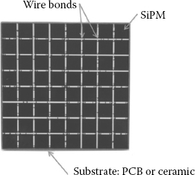
FIGURE 15.20 (See color insert) Epoxy-coated ceramic carrier SiPM array. This example is a 8 × 8 array of 6 × 6 mm2 SiPMs mounted on a PCB substrate.

FIGURE 15.21 Comparison of PDE versus wavelength measured on bare die, poured epoxy, clear MLP, and TSV package types.
1. Inconsistent PDE due to variations in optical transmission, particularly at short wavelengths.
2. Degradation in optical transmission during operating life (“yellowing” of the organic epoxy).
3. Nonuniformity of adhesion to the die surface. This will result in delamination during the operating life and consequent loss of transmission or failure of the wire-bond interconnects.
4. Nonuniformity and high values of mismatch between the thermal expansion coefficient of the epoxy and that of the substrate and wire bonds, leading to failure of the wire bonds.
5. Poured epoxy products require a package sidewall to contain the epoxy. Consequently, there is always dead space at the edges of the array. This adds dead space between arrays that are placed beside other arrays and limits the total fill factor.
6. Connection to the array must also be made to the back of the substrate. This increases the PCB traces and connections between the sensor and the subsequent read-out electronics, which can degrade the performance when compared with the other package technologies discussed here.
TABLE 15.2
Summary of Comparison Points for SiPM Array Package Options
Requirement |
Poured Epoxy |
Clear MLP |
TSV |
Array fill factor |
Near optimum |
Limited by peripheral leadframe |
Optimum |
Optical transmission |
Poor |
Good |
Best |
Operating conditions |
0°C–40°C |
–40°C to 85°C |
–40°C to 95°C |
Reliability |
Manual processing: reduced reliability |
Good |
Best |
Service life |
Yellowing of potted epoxy is not well controlled |
Good |
Best |
Uniformity and reproducibility |
Poor |
Good |
Good |
Cost |
Low cost for laboratory use: not recommended for use in volume arrays |
Lowest high-volume sensor cost: low array assembly costs |
Highest high-volume sensor cost: low array assembly costs |
A summary of the most important points related to the poured epoxy package are detailed in Table 15.2.
15.6.2 CLEAR MICRO LEADFRAME PACKAGE
The clear MLP process entails attaching SiPMs to a large leadframe with die attach epoxy, wire bonding the SiPM contact pads to the leadframe terminals, molding in clear compound, and sawing into individual packages. Since the SiPMs are mounted onto a much larger leadframe, a fully automated process can be used in their manufacture. A drawing of a clear MLP SiPM is shown in Figure 15.22a. This figure details the SiPM placement on the leadframe, the wire-bond placement, and the clear molding compound that encases the SiPM. Examples of three different sizes of clear MLP-packaged SiPM are shown in Figure 15.22b. This figure shows 6 × 6, 3 × 3, and 1 × 1 mm2 SiPM sensors. The back contact of the sensor is shown at the top of Figure 15.22b.
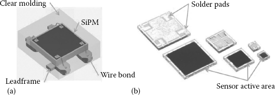
FIGURE 15.22 (See color insert) (a) Clear micro leadframe package drawing. (b) Images of the top and back side of 1 × 1, 3 × 3, and 6 × 6 mm2 SiPM-packaged sensors.
The epoxy in a clear MLP is molded and cured at temperatures between 140°C and 160°C. The material and mold process is more controllable than the mixed and poured epoxy process described in Section 15.6.1. The MLP SiPMs have the following key benefits over poured epoxy SiPMs:
1. Better control of optical properties and thermal expansion/contraction of the material during operating life.
2. A flatter more uniform surface and optical interface allows better coupling to scintillation crystals.
3. Clear MLP SiPM sensors can be surface mounted directly to the read-out PCB and it is possible to minimize the PCB trace length and reduce the number of connectors in a large-area array.
4. A moisture sensitivity level (MSL) of 3 can be obtained which allows 168 h of ambient humidity exposure before the part needs to be soldered to a PCB.
5. Clear MLP sensors can be soldered using standard reflow solder conditions at 260°C.
6. MLP materials and processing are suited to high-volume manufacturing and provide the lowest cost product compared with any other package suitable for arrays.
7. Arrays can be fabricated with minimal dead space at the edge. This allows arrays to be tiled at a constant sensor pitch.
Examples of four different types of arrays, manufactured using clear MLP sensors, are shown in Figure 15.23. In all cases, these arrays were assembled on a PCB with 0.2 mm of dead space between sensors. The largest size array is the 8 × 8 array of 6 × 6 mm2, which is 57.4 mm per edge. For this array, the sensors were placed on a 7.2 mm pitch. The pitch comprises a 6 mm sensor, 1 mm of package dead space, and 0.2 mm of dead space between packages. The 1 × 1 mm2 sensor is packaged in a 1.5 × 1.8 mm2 package enabling a high fill factor.
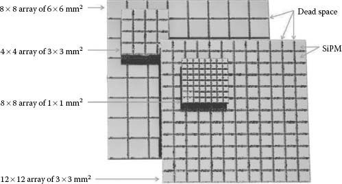
FIGURE 15.23 Example of four different large-area arrays of clear MLP arrays sensors mounted on a PCB. The dead space between the clear MLP sensors is 200 μm.
In addition to the performance and reliability benefits of the clear MLP, the flexibility to define the array size through the PCB layout and the ability to use high-volume PCB manufacturing, mean that the clear MLP is considered a superior package type to those utilizing poured epoxy.
Both poured epoxy and clear MLP require packaging of the die after they have been processed. TSV packaging, however, is a wafer-level package and is made while the die are still on the wafer and have not yet been singulated. A true wafer-scale TSV process entails bonding a glass substrate to the top of the silicon wafer and back-grinding the silicon to a thin layer. Vias are etched in the silicon and metal is deposited to make contact with the terminals in the die. Solder bumps are attached to the deposited metal on the back side of the sensor. The wafer is then sawn into individual die and can be placed onto a PCB substrate using a similar process to that used to manufacture clear MLP arrays. An example of a TSV-packaged SiPM is shown in Figure 15.24a. The corresponding cross section of an SiPM TSV sensor is shown in Figure 15.24b.
The performance of a TSV-packaged SiPM brings the PDE closer to the bare-die PDE curve, as shown in Figure 15.21. This is because the TSV glass is more transmissive at short wavelengths than the organic materials used in poured epoxy and clear MLP products. The additional benefits of a TSV-packaged SiPM are as follows:
• Transmission in glass is stable during operating life. The yellowing seen in organic compounds does not occur in glass and TSV products have the longest operating lifetime.
• There are no wire bonds so each TSV component will be the same size as the sensor. This optimizes the fill factor allowing the highest density arrays to be produced. This high fill factor is shown in Figure 15.25.
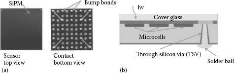
FIGURE 15.24 (a) TSV SiPM example showing top sensor side and bottom contact side. (b) TSV cross-section example.
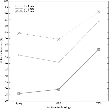
FIGURE 15.25 Comparison of the fill factor between poured epoxy, clear MLP, and TSV package types when placed in an array.
• The failure mechanisms associated with wire bonds and epoxy are absent. Therefore, TSV products will have the highest reliability of any SiPM package.
• TSV packages are MSL 1 compatible, reducing costs at PCB contract manufacturers.
• TSV processing is inherently conducive to tight control and high volume.
• TSV can be placed into arrays with low dead space between sensors. Due to excellent wafer saw tolerances, the dead space between TSV die in arrays can be 0.1 mm. This improves the overall TSV package fill factor compared with clear MLP.
The key disadvantage of the TSV package is a slightly increased cost compared with clear MLP. It is up to the user to decide if the advantages outweigh a sensor cost increase in their product design.
The following figures and table summarize the various packages discussed in this section. Figure 15.21 compares the PDE measured wavelength for four differently packaged 3 × 3 mm2 SiPM sensors. All data have been normalized to allow easy comparison between package types. To provide a baseline of the core performance, the bare-die curve was obtained with an SiPM mounted directly onto the substrate with no poured epoxy over the surface area. It therefore represents the PDE of the sensor. The epoxy curve represents typical PDE measured with poured epoxy products, which is characterized by a reduced peak PDE due to transmission losses in the epoxy. The clear MLP package has better peak PDE than the poured epoxy but does have a short wavelength cut-off at 320 nm due to the clear molding compound. The TSV package curve demonstrates the best performance at the peak wavelength and a greatly improved performance in the ultraviolet (UV) range. The TSV package most closely approximates the bare-die curve and represents the highest performance package for the highest PDE.
A comparison of the fill factors of various package types was performed using the detailed knowledge of each SiPM sensor size; 1 × 1, 3 × 3, and 6 × 6 mm2 combined with typical design rules for contract manufacturer placement of sensors into arrays. In all cases, the TSV package provides the highest package fill factor possible when creating large-area arrays due to the low dead space. A comparison of the three package technologies is summarized in Table 15.3.
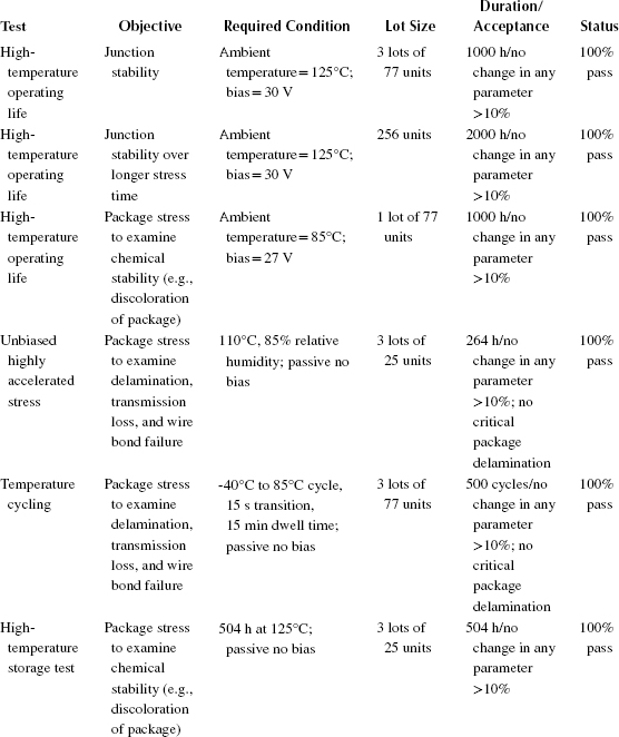
In this section, the reliability stress assessment completed on SiPMs will be discussed. Additionally, the justification for the adoption of industry standard reliability stress assessment flows from the Joint Electron Device Engineering Council (JEDEC) will be reviewed.
15.7.1 ISSUES OF SIPM RELIABILITY ASSESSMENT
SiPM sensor reliability is a key requirement for high-volume applications. At present, there is a lack of industry-accepted standards for reliability assessment of SiPM sensors. This is believed to be due to the varied and complex manufacturing processes required for optical sensors. This is contrasted with the integrated circuits industry where there are strong standards that are widely adopted and used for assessing the reliability of products. As the sensors discussed in this chapter are developed using CMOS, high-volume fabrication facilities, it is applicable and desirable to follow the standards adopted by the integrated circuits industry. A major publisher of standards used by the integrated circuits industry is JEDEC [20], which freely publishes test standards that can be adopted by manufacturers to assess product reliability. For the reliability assessment of SiPMs, the JEDEC standards have been adopted.
15.7.2 RELIABILITY ASSESSMENT OF SIPMs
All stress and test steps were carried out as per the JEDEC standard conditions. The JEDEC standard for the main reliability test procedure can be obtained from the JEDEC [19]. To assess the silicon reliability, SensL used a combination of the standard commercial packages available, including SensL clear MLP, and metal can (TO5 style) packages with sealed lids containing an optical window. The use of TO5 style packages was a requirement for the high-temperature stress tests designed to test the reliability of the silicon, independent of the package material. For the assessments, packaged die were obtained typically from three separate silicon fabrication lots and were packaged as required. All tests were made in accordance with the relevant JEDEC standards referenced in Table 15.3. Of significant note from Table 15.3 are the high temperature operating-life tests that were completed to 1000 h with an additional higher endurance stress to 2000 h. This represents the longest high-temperature stress to date on a statistically relevant sample set of SiPMs that the authors have seen reported.
All SensL SiPM sensors passed the tests. An example of the PDE measured before and after a high-temperature operating-life stress test is shown in Figure 15.26. No change in performance was observed.
As can be seen, further stress data were taken to assess product reliability, including temperature cycling, moisture and humidity stressing, and high-temperature storage. The excellent results demonstrate that the SiPM manufacturing process is robust and enables the production of reliable, high-quality sensor components.
For high-volume applications, the reliability of the product is a key concern. It is believed that the adoption of the reliability assessment standards used by integrated circuit manufacturers provides the most comprehensive method to assess SiPM product reliability. The standard methods outlined by the JEDEC have been applied to B-Series SiPMs from SensL, with all parts passing standard reliability assessment flows. The adoption of integrated circuit industry standard reliability test flows is considered of vital importance for the adoption of the SiPM in high-volume applications.
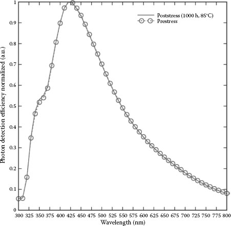
FIGURE 15.26 Measurement of PDE pre- and poststress. The stress condition is 85°C for 1000 h.
15.8 SCINTILLATION CRYSTAL READOUT
The focus of this section is on the use of scintillation crystals for the detection of gamma rays. Such crystals are used for a variety of applications related to medical imaging and radiation detection. Both markets use a combination of a scintillator and an optical sensor to detect gamma rays.
A gamma-ray detector must detect, amplify, and output an electrical signal that accurately conveys the gamma-ray energy and in some cases the photon arrival time. The most common type of gamma-ray detector relies on a combination of scintillation crystal and optical sensor, as shown in Figure 15.1. A variety of crystals are available that can be used to convert the gamma radiation into optical photons and the work of Dorenbos [21] shows a useful time line of the development and performance limits for various crystal types. Some of the most popular scintillators, such as LaBr3, LYSO, BGO, and CsI(Tl), which are relevant to PET and radiation detection will be considered in this chapter. These crystals have a variety of primary characteristics such as light yield, density, emission wavelength, and decay time, which directly impact the overall performance of the crystal and optical sensor assembly. Typically, to optimize the performance of a gamma-ray detector, the goal is to maximize the number of optical photons that are detected from the scintillator while minimizing the amount of noise coming from the optical sensor.
Figure 15.5 shows the normalized light yield for a variety of standard scintillation crystals that are used for radiation detection. The data for Figure 15.5 were obtained directly from the datasheets available for each crystal type from Saint-Gobain [22] and are in agreement with published data found in the extensive scintillation crystal database made available online by Derenzo [23]. The photon emission has been digitized from the manufacturer’s datasheets and normalized according to the peak light yield, which is expressed in photons per kiloelectron volt. A high light yield and an emission spectrum matched to the sensitivity of the SiPM will typically improve detection performance.
Another parameter that plays an important role in the performance of radiation detectors is the emission decay time. Typical decay times for the crystals discussed in this chapter are shown in Table 15.4. The decay time of the crystal determines the amount of time required for a measurement and the amount of noise that will be integrated during the signal acquisition. Longer measurement times lead to increasing amounts of noise included in the recorded signal.
The refractive index of the crystal is also important as this will determine the light coupling between the crystal and the sensor. Mismatched refractive indices lead to Fresnel losses of photons transitioning from the scintillation crystal to the optical sensor. Index-matching coupling material should always be used between an SiPM sensor and a scintillation crystal for optimum light collection.
The scintillation crystal emission and the decay time of the scintillator combined with the sensors’ sensitivity and noise play a large role in optimizing the radiation detector performance. Additional scintillation crystal parameters such as density, thermal expansion coefficients, hygroscopic nature, and cost will also play a role in determining the suitability of a detector for a given application but these are outside the scope of this chapter on SiPM sensors.
TABLE 15.4
Typical Crystal Information from Saint-Gobain and Energy Resolution Obtained in the Literature from Dorenbos

Source: Saint-Gobain, http://www.crystals.saint-gobain.com/; Dorenbos, P., IEEE Trans. Nucl. Sci., 57, 1162, 2010.
15.8.2 ENERGY RESOLUTION AND COINCIDENCE TIMING MEASUREMENTS
Applications involving scintillation materials fall into two main application areas: those that require fast timing and those for spectroscopy requiring optimum energy resolution. These two application areas have slightly diverging requirements in the scintillating crystals used and in the optimal operating voltage settings for the sensor. For fast-timing applications, a high light yield scintillator with a fast rise and short decay time is required. For applications requiring the best (lowest) energy resolution, the nonproportionality of the crystal is a driving factor to obtain the lowest energy resolution. Energy resolution values that have been obtained in the literature are summarized in Table 15.4.
For the best energy resolution measurements, the maximum of the sensor PDE should be matched as closely as possible to the peak wavelength of the scintillator. The energy resolution percentage (full width at half maximum [FWHM]) is related to both the sensor performance as well as the crystal. A good review of this is found in the work by Dorenbos [21] and Grodzicka [24], which determines the energy resolution through the following equation:
(15.12) |
where:
Rin |
is related to the crystal inhomogeneity from crystal quality, wrapping variation, and crystal finish differences |
Rnp |
is due to the nonproportional response of the scintillator |
Rstat |
is related to the photon detection statistics and the excess noise of the SiPM |
Rstat |
is given by the following equation [25], which has been modified to include the dark count rate in Equation 15.13: |
(15.13) |
In this equation, Ndp is the number of detected photons and Ndc is the number of dark counts during the measurement integration time. ENF is the excess noise factor. An ENF of 1 is a perfect detector while an increasing ENF degrades Rstat. The ENF for the SiPM is dominated by cross talk and afterpulsing. These unwanted effects increase the variability in the output of the SiPM. When used in a detector, increasing the overvoltage will increase PDE and therefore the number of detected photons, Ndp; however, cross talk and afterpulsing will also increase, which can degrade the energy resolution obtained. For typical PET applications looking at signal levels from 511 keV gamma rays, Rstat is the predominant factor while Rdcr dominates measurements at lower energies.
For coincidence timing measurements the scintillating crystal emission should be short and the PDE and rise time of the sensor should be high. Cross talk, afterpulsing, and dark count rates are considered secondary factors until high overvoltages are reached. This operating point is best determined experimentally as it depends on the scintillator, sensor, and read-out method. Crystals for use in fast coincidence timing measurements emit light in the blue to UV portion of the spectrum [21]. The SiPM sensors shown in this chapter have been optimized to allow the detection of these short wavelength emission crystals.
15.8.3 SIPM SCINTILLATION CRYSTAL PERFORMANCE
To demonstrate the performance of the SensL SiPM in an application environment, the sensors were coupled with cerium-doped lutetium yttrium orthosilicate (LYSO:Ce) scintillation crystals. This is similar to the system configuration in a PET time-of-flight (ToF) system. When the SiPM sensor is combined with the scintillation crystal, it forms a gamma-ray detector. It is desirable to demonstrate a minimum energy resolution and a minimum coincidence resolving time (CRT) for the pair of 511 keV gamma rays that are produced in electron-positron annihilation. LYSO is well matched to the sensor PDE presented in Figure 15.8 as the output peak at 420 nm matches the photon detection peak of the sensor. The measurement setup for energy resolution and CRT is shown in Figure 15.27. This shows the crystals in “head-on” configuration, which more closely mimics the way that crystals are positioned in a standard PET system. The crystals are directly mounted on the SiPM using coupling grease (BC-630) [22] and amplifiers are used to amplify the output voltage level to an appropriate range for the Wavecatcher USB digitizer [26]. A variety of amplifier combinations can be chosen to suit most crystal testing needs [27].
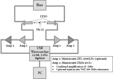
FIGURE 15.27 Example of the energy resolution and coincidence resolving time (CRT) experiment setup used in this work.
15.8.4 COINCIDENCE RESOLVING TIME
CRT is an important PET ToF system measurement parameter. A low CRT allows a more accurate determination of the emission source position through triangulation. For this work, CRT was evaluated by determining the arrival time of coincident 511 keV photon pairs at a corresponding pair of scintillation-based detectors. For this measurement, a 22Na 511 keV source was placed between two facing 3 × 3 × 20 mm3 LYSO coupled to SiPM sensors, positioned head-on, and the resulting electrical signal from the detectors was amplified and recorded with a high-speed digitizer (USB Wavecatcher 12-bit, 3.2 GS/s). In analyzing the resulting pairs of signal traces, energy filtering was performed at ±9% around the peak value selecting signals that the charge integral matched with the peak in the charge spectrum attributed to 511 keV; time walk correction was performed removing the correlation between the energy difference and the time difference of the scintillator pairs. In addition, the optimal choice of the leading-edge threshold to timestamp each of the electrical signals further optimized the CRT value. Figure 15.28 shows typical CRT histograms measured on the fast output of the 30035 SiPM. Similar results have been shown in the literature [28,29].
Measurements on standard anode–cathode signals were also performed and a value of 306 ± 3 ps was obtained. The fast output provides superior results due to its fast signal rise time, low output capacitance, and low parasitic impedance.
In energy resolution measurements, the detector principle is that of a proportional counter, in that the number of scintillation light photons are proportional to the energy of the gamma photon penetrating the crystal. Integrating the electric signal from the sensor during each scintillation event and then binning the result yields a spectrum of counts versus an observable proportional to the gamma photon energy.
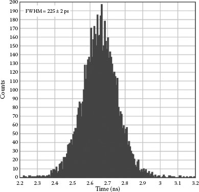
FIGURE 15.28 Coincidence resolving time measured for sample pairs of a 30035 SiPM.
To determine the energy resolution for a typical PET setup, a 3 × 3 × 20 mm3 LYSO crystal was coupled to a 30035 SiPM sensor using BC-630 silicone optical grease from Saint Gobain. The SiPM was biased at 5 V over the breakdown voltage, and the signal from the SiPM was amplified and traces were recorded using a highspeed digitizer.
The energy resolution spectrum for a 30035 SiPM is shown in Figure 15.29. This measurement was made from the fast output signals and was similar to measurements taken on the standard anode–cathode output. When coupled to a relatively bright and fast crystal such as LYSO, the signal from the fast output is sufficient to accurately represent the signal pulse and an accurate energy resolution plot can be obtained. For this measurement, the energy resolution was limited by the crystal proportionality, statistical uncertainty in photon counting by the sensor, and electrical noise in the sensor and associated electronics.
Additional work on measurements using CsI(Tl) can be found in the work of Becker [30] who details a compact and portable gamma spectrometer measurement system that achieves 5.66% energy resolution.
This chapter has demonstrated the operation of SiPMs developed for high-volume CMOS fabrication. The review started from the basic physics of the operation of SiPMs and linked various key operating parameters such as the breakdown voltage and the wavelength sensitivity to the physical structure of the sensor. The main SiPM parameters were reviewed including PDE, dark count rate, gain, cross talk, afterpulsing, and dynamic range. The key highlights show that a PDE of 41% and low dark count rates of <100 kHz can be obtained with low afterpulsing and cross-talk rates. The manufacturability and high-volume production of SiPMs were demonstrated through wafer-level electrical and optical testing of over 204k SiPM sensors demonstrating excellent breakdown voltage, dark current, and optical uniformity. A review of the packaging requirements and suitable packages for large-area arrays was presented demonstrating the key parameter trade-offs such as PDE, fill factor, and cost. It was shown that clear MLP- and TSV-packaged sensors have clear advantages for high-volume array applications. For the reliability assessment of the SiPM, industry standard integrated circuit testing procedures were adopted. The tests are believed to provide a comprehensive testing regime for SiPMs and should be used for SiPM product qualification. The use of SiPMs for scintillation crystal readout was reviewed theoretically and a clear demonstration of the high performance that can be obtained was shown with LYSO:Ce. CRT of 225 ps and energy resolutions of 9.2% were obtained experimentally.
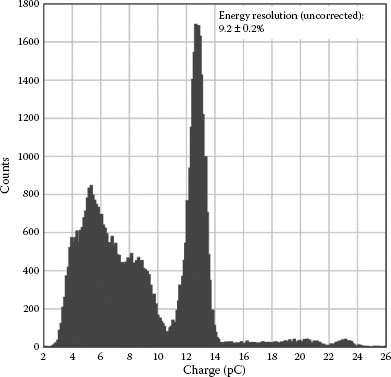
FIGURE 15.29 Charge spectrum full width half maximum measured on fast output for a 30035 SiPM.
1. R. H. Haitz, Model for the electrical behavior of microplasma, J. Appl. Phys., 35(5), 1370–1376, 1964.
2. R. H. Haitz, Microplasma interaction in silicon p-n junctions, Solid-State Electron, 7, 439–444, 1964.
3. R. H. Haitz, Mechanisms contributing to the noise pulse rate of avalanche diodes, J. Appl. Phys., 36,(10), 3123–3131, 1965.
4. R. H. Haitz, Studies on optical coupling between silicon p-n junctions, Solid-State Electron, 8, 417–425, 1965.
5. W. G. Oldham, et al., Triggering phenomena in avalanche diodes, IEEE Trans. Electron Devices, 19(9), 1056–1060, 1972.
6. R. J. Mclntyre, Multiplication noise in uniform avalanche diodes, IEEE Trans. Electron Devices, ED-13, 164–168, 1966.
7. R. J. Mclntyre, On the avalanche initiation probability of avalanche diodes above the breakdown voltage, IEEE Trans. Electron Devices, 20(7), 637–641, 1973.
8. S. Cova, et al., Towards picosecond resolution with single-photon avalanche diodes, Rev. Sci. Instrum., 52(3), 408–412, 1981.
9. R. G. W. Brown, et al., Characterization of silicon avalanche photodiodes for photon correlation measurements. 1: Passive quenching, Appl. Opt., 25(22), 4122–4126, 1986.
10. R. G. W. Brown, et al., Characterization of silicon avalanche photodiodes for photon correlation measurements. 2: Active quenching, Appl. Opt., 26(12), 2383–2389, 1987.
11. V. Saveliev, et al., Silicon avalanche photodiodes on the base of metal-resistor-semiconductor (MRS) structures, Nucl. Instrum. Methods Phys. Res. A, 442, 223–229, 2000.
12. D. Bisello, et al., Metal-resistive layer-silicon (MRS) avalanche detectors with negative feedback, Nucl. Instrum. Methods Phys. Res. A, 360, 83–86, 1995.
13. V. Golovin, et al., Limited Geiger-mode microcell silicon photodiode: New results, Nucl. Instrum. Methods. Phys. Res. A, 442, 187–192, 2000.
14. A. B. Kravchenko, et al., A linear array of avalanche MIS photodetectors, Sov. J. Quantum Electron., 8(11), 1399–1400, 1978.
15. A. B. Kravchenko, et al., Feasibility of construction of a pulsed avalanche photodetector based on an MIS structure with stable internal amplification, Sov. J. Quantum Electron., 9(9), 1086–1089, 1978.
16. M. Polyanskiy, Silicon refractive index, Refractive Index Database, http://refractiveindex. info, accessed June 2014.
17. J. T. M. de Haas, et al., Advances in yield calibration of scintillators, IEEE Trans. Nucl. Sci., 55, 1086–1092, 2008.
18. SensL B-Series Datasheet, Fast, Blue-sensitive silicon photomultiplier sensors, http://www.sensl.com/downloads/ds/DS-MicroBseries.pdf, accessed June 2014.
19. P. Eckert, et al., Characterisation studies of silicon photomultipliers, Nucl. Instrum. Methods Phys. Res. A, 620, 217–226, 2010.
20. JEDEC Standards Organization, Global Standards for the Microelectronics Industry. http://www.jedec.org/, accessed June 2014.
21. P. Dorenbos, Fundamental limitations in the performance of Ce3+, Pr3+, and Eu2+ activated scintillators, IEEE Trans. Nucl. Sci., 57, 1162–1167, 2010.
22. Saint-Gobain, http://www.crystals.saint-gobain.com/.
23. S. Derenzo, Scintillation Properties, Lawrence Berkeley National Laboratory, http://scintillator.lbl.gov/, accessed June 2014.
24. M. Grodzicka, et al., MPPC array in the readout of CsI:Tl, LSO:Ce:Ca, LaBr3:Ce, and BGO scintillators, IEEE Trans. Nucl. Sci., 59(6), 3294–3303, 2012.
25. M. Moszynski, et al., A comparative study of silicon drift detectors with photomultipliers, avalanche photodiodes and PIN photodiodes in gamma spectrometry with LaBr3 crystals, IEEE Trans. Nucl. Sci., 2009.
26. Wavecatcher USB Digitizer, http://www.heptech.org/Phocea/file.php?file=Ast/140/fiche_LAL_Wave_Catcher.pdf, accessed June 2014.
27. Mini Circuits website, RF Electronics Engineering, http://www.minicircuits.com, accessed June 2014.
28. S. Dolinsky, et al., Timing resolution performance comparison for fast and standard outputs of SensL SiPM, IEEE NSS/MIC]2013.
29. J. Y. Yeom, et al., Fast timing silicon photomultipliers for scintillation detectors, IEEE Photon. Technol. Lett., 25, 1309–1312, 2013.
30. E. Becker, The MiniSpec: A low-cost, compact, FPGA-based gamma spectrometer for mobile applications, thesis, http://ir.library.oregonstate.edu/xmlui/handle/1957/42365, accessed June 2014.
* Icap is available in products from SensL to allow for a low capacitance and fast output. Other SiPMs will not contain Icap.
* Fast output capacitors are only included in SiPMs provided by SensL.