
CONTENTS
11.2 Organic Semiconducting Single-Crystal Growth
11.3 Organic Semiconducting Single-Crystal Properties
11.4 X-Ray Electrical Photoresponse
The detection of ionizing radiation is an important task for a number of technologically and socially relevant activities, ranging from environmental monitoring to industrial, security, and health applications. As such, a large variety of detectors for ionizing radiations have been developed in the past, based either on gas-filled containers (such as ionization chambers or Geiger counters), on solid or liquid materials capable of producing visible photons upon exposure to the radiation (scintillators), or on gaseous, liquid, or solid materials (or a combination of them) capable of visualizing the track of ionizing particles (cloud chambers, bubble chambers, spark chambers, silicon detectors, etc.). Ionizing radiation detectors may also be categorized as being “direct” or “indirect” detectors. A “direct detector” is one in which the incoming ionizing radiation is transduced by a sensor directly into an electrical signal. In an “indirect detector,” the transduction occurs in a two-step process, the first step being performed by a first sensor (for example, a scintillator) and the second step being performed by a second sensor (for example, a photodiode). Indirect detectors are therefore constituted of two (or more) sensors, complemented by a signal amplifying/processing unit. This approach induces a loss of information in the process, especially at low radiation doses, and, most importantly, a rather complex and fragile device structure. State-of-the-art direct detectors are made with inorganic semiconductors, such as silicon, cadmium telluride, and gallium nitride, in which the incoming radiation directly generates electron–hole pairs that constitute the collected output electrical signal. However, some of these materials (e.g., Si, Ge) have less than ideal bandgap widths and show high dark currents, making them unattractive candidates for room-temperature operation, while others contain a large number of defects and electrically active impurities that affect the recombination and collection processes of the photogenerated carriers, as well as detector stability under irradiation and polarized operation. In general, to achieve a high radiation-detection efficiency it is necessary to have materials that exhibit a very low dark current (<10-7 A), and thus possess a high resistivity (>109 Ωcm). Large-area x-ray-detecting panels for digital imaging have been developed for medical applications, but are mostly based on the “indirect detection” approach, with amorphous silicon (or other inorganic semiconductors) coated by a scintillator material. The complexity of these devices and the high fabrication cost of detector-grade inorganic semiconductors limit their application in other fields. The main drawbacks of such large-area detectors are the poor conversion efficiency and signal-to-noise ratio typical of indirect detecting systems, plus the high cost, not taking into account the high complexity of operation (requiring trained operators). Therefore, alternative materials and technologies enabling the fabrication of direct detectors on large areas and at acceptable prices have to be sought.
Organic materials have recently attracted major attention because they demonstrated, in the case of other electronic/optoelectronic devices (e.g., transistors and light-emitting devices), room-temperature operation, low environmental impact, low fabrication costs, and the possibility of fabricating transparent and flexible devices, allowing unprecedented and integrated device functions and architectures [1,2,3,4,5,6,7].
As detectors of ionizing radiation, organic semiconductors have so far been mainly proposed in the indirect-conversion approach, either as scintillators [8,9] or as photodiodes [10,11,12], which detect visible photons coming from a scintillator and convert them into an electrical signal. A few examples of organic materials used for the direct detection of radiation have been recently reported in the literature, referring to semiconducting or conducting polymer thin films, or charge-transfer-conducting organic crystals. Interestingly, it has been shown that thin films based on semiconducting polymers can withstand high x-ray doses without significant material degradation [13]. However, to obtain this result, the polymers must be properly encapsulated to protect them from environmental oxygen and water; otherwise, significant degradation of the device occurs rapidly [14]. It has to be noted that effective encapsulation of semiconducting polymer-based devices leads to markedly increased production costs and complexity of device geometry. A few thin-film, organic-based direct detectors have been reported recently, but they rely on the presence in the detector of metallic electrodes or intentionally introduced metallic or semimetallic nanoparticles, which act as sources of secondary photoelectrons, to produce reasonable photoconversion efficiencies [13,15,16,17,18,19,20,21].
We recently showed that organic semiconducting single crystals (OSSCs) can be used as effective direct x-ray detectors. In particular, devices based on solution-grown OSSCs (from two different molecules: 4-hydroxycyanobenzene [4HCB] and 1,8-naphthaleneimide [NTI]) (Figure 11.1) have been fabricated and operated in air, under ambient light, and at room temperature, at voltages as low as a few tens of volts, delivering highly reproducible performances and a stable linear response to the x-ray dose rate, with notable radiation hardness and resistance to aging [22].
The role of high-atomic number components (e.g., metals) in the device response has been elucidated, evidencing the intrinsic response of the organic crystals to x-rays, which allowed the fabrication of well-performing all-organic and optically transparent devices.
It is important here to remember how the use of single crystals has been fundamental to the development of semiconductor microelectronics and solid-state science. Whether based on inorganic [23,24] or organic [25,26] materials, the devices that show the highest performance rely on single-crystal interfaces, due to their nearly perfect translational symmetry and exceptionally high chemical purity. Moreover, organic single crystals show band-like transport behavior [27], and top-performing rubrene single crystals (vapor grown, only a few microns thick) have been recently reported to reach hole mobilities of 40 cm2 V-1 s-1 [28] and electron mobilities up to 11 cm2 V-1 s-1, measured in a field-effect transistor configuration, which allows the current flowing through the crystal to be controlled and amplified [29,30,31,32]. The same crystals, when sufficiently thin (i.e., less than 3 μm), are reportedly conformable/flexible [33].
The observed performance indicates that OSSCs are very promising candidates for a novel generation of low-cost, room-temperature x-ray detectors, which will allow unprecedented applications to be developed in the radiation-detector research field, mostly complementary to the high-performance ones presently based on inorganic semiconductors.
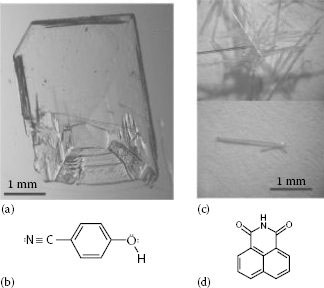
FIGURE 11.1 Single crystals and molecular structures of 4HCB (a,b) and NTI (c,d).(From Fraboni, B. Ciavatti, A. Merlo, F., Pasquini, L., Cavallini, A., Quaranta, A., Bonfiglio, A., and Fraleoni-Morgera, A.: Adv. Mater. 2012. 24. 2289. Copyright Wiley-VCH Verlag GmbH & Co. KGaA. Reproduced with permission.)
11.2 ORGANIC SEMICONDUCTING SINGLE-CRYSTAL GROWTH
OSSCs are usually grown using chemical vapor deposition (CVD), which involves the use of multizone heated tubes, in which a vapor of molecules is carried by a convenient inert gas onto cold walls. The molecules condense onto these walls, and tight control over the temperatures of the system is necessary to encourage them to form a good crystal [29,34]. However, this method is rather sensitive to system perturbations (mainly temperature and carrier gas flow variations), and it is time and energy intensive. In addition, it is well documented that even small amounts of impurities can have a dramatic impact on the OSSCs’ transport properties [35,36], and the CVD method is not particularly effective in getting rid of these impurities, unless repeated and slow cleaning/deposition cycles are performed. Finally, due to the nature of this growth process, it is difficult to grow very large crystals. Crystal growth from the melt could represent an interesting alternative to CVD. Starting from a melt that can be contained in an arbitrary vessel (provided, of course, that the latter is able to withstand the melting conditions), this process does not have tight constraints in terms of final crystal size. Moreover, consistent know-how on this technique is available from inorganic materials for electronic applications, in which crystallization from the melt has become a scientific and technological field of its own [37]. Nonetheless, although in some cases crystallization of OSSCs from the melt has proved to be successful [38], stability problems (especially due to enhanced photooxidation rates at temperatures approaching melting temperature) often limit the possibility of taking advantage of this crystallization technique for organic materials.
These problems may be overcome using growth from solution. This approach has high versatility, with the capability to deliver very large (up to several cubic centimeters) and pure crystals, low energy requirements (i.e., no need for dramatic heating, cooling, or vacuum), and ease of implementation. This latter point is worthy of particular attention, since it implies extremely low costs, especially when areas as large as square meters are projected to be covered with single crystals (as would be necessary, for example, for flexible, large-area ionizing-radiation detectors aimed at monitoring landfills or seaports). Moreover, solution growth allows good control over many crystal properties, including size and even the developed crystallographic phase [39]. A partial drawback of solution growth is its relative slowness, due to the small amounts of matter that are involved in the process, especially in dilute solutions. In fact, for applications such as nonlinear optics, where crystals having centimeter-long sides are needed, at least for fundamental studies, several days (often weeks) of growth are needed to obtain a crystal of satisfactory size [40,41]. On the other hand, many applications, such as organic electronics, do not require such large crystals, and a suitable crystal size may be as low as the nanometer or micrometer range [42], though most common sizes are around hundreds of microns—a few millimeters [26,28,43]. Solution growth has also been used to produce organic (not necessarily semiconducting) single crystals used as scintillators in ionizing-radiation detectors [44,45], demonstrating that this technique delivers crystals able to usefully interact with ionizing radiation. In addition, solution-grown OSSCs have repeatedly demonstrated good electronic quality [43,46].
In this regard, it was recently reported that single crystals based on solution-grown 4HCB (Figure 11.1a and b) are able to detect x-rays via direct generation of electrical current on x-ray irradiation [22]. 4HCB crystals have rather complex crystal unit cell structures, which we have characterized by x-ray diffraction (XRD) methods (Figure 11.2), and which result from enhanced hydrogen-bond formation between the –OH and –CN groups of the molecule [47,48]. Despite this structural complexity, they present marked reproducibility of their electronic properties (mobilities, traps density, etc.) over tens of crystals having different sizes, deriving from different batches, and even grown in different conditions (in terms of temperature, initial solution concentration, etc.) [49,50].
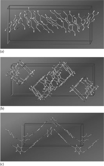
FIGURE 11.2 (See color insert) Simplified views of the 4HCB crystalline unit cell, seen along the crystallographic axes a (green axis), b (red axis), and c (blue axis). (From Fraboni, B., Femoni, C., Mencarelli, I., Setti, L., Di Pietro, R., Cavallini, A., and Fraleoni-Morgera, A.: Adv. Mater. 2009. 21. 1835. Copyright Wiley-VCH Verlag GmbH & Co. KGaA. Reproduced with permission.)
A further point of advantage of 4HCB crystals is that they can be easily grown from widely available solvents/nonsolvents, such as ethylic ether or petroleum ether, and their size can be controlled by working on parameters such as the solvent/nonsolvent volume ratio or the 4HCB concentration in the starting solutions [51]. The single crystals obtained in this way are very robust to physical manipulation (they can be easily moved and positioned on substrates, electrode arrays, sample holders, etc.) and to environmental conditions (normal atmosphere, light, room temperature). The possibility of tuning the crystal size with simple changes of the growth recipe is of particular importance in view of a thorough understanding of their functional properties.
Another possibility offered by the versatility of the solution growth technique is to obtain crystals directly grown onto substrates constituted by a thin dielectric layer (SiOx) thermally grown on doped Si, so to constitute a native field-effect-transistor (FET) substrate. The crystals obtained in this way were tested under synchrotron-originated polarized IR spectroscopy as bare crystals or as the active channels (after source and drain upper electrodes were fabricated on the crystals, as shown in Figure 11.3) in operating FETs, revealing interesting and in some ways surprising crystal polarization effects due to gating, which apparently develops a charge transport layer either with marked metallic behavior or much thicker (on the order of several hundreds of microns) than currently assumed to be the case for these systems [52].
The possibility of growing OSSCs from solution does not only offer exciting chances of performing fundamental studies, but, even more interestingly, paves the way for promising applications of these materials in practical devices.
In fact, it has been recently shown that it is possible to fabricate high-quality OSSCs via inkjet printing [53] or shear-aided crystallization [54] (Figure 11.4). These intriguing technological possibilities highlight the potential for large-area fabrication of arrays of OSSCs-based devices. In particular, this is true for large-area, composite devices (which represent by far the largest class of electronic products today, and the most desired goal for the whole field of organic optoelectronics). In this frame, the accurate and reproducible placement of OSSCs onto electrode matrices or in precise positions onto a given substrate still represents a challenge far from being solved. Crystal growth from solution, thanks to its unique cocktail of low costs, rapid production times (when small crystals are considered), low energy requirements, and manufacturing versatility, could well represent a viable fabrication pathway for solving this problem, opening the way for a truly widespread organic electronics.
FIGURE 11.3 Layout of a 4HCB single-crystal-based device probed under FT-IR linearly polarized light. (Reproduced with permission from Fraleoni-Morgera, A., Tessarolo, M., Perucchi, A., Baldassarre, L., Lupi, S., Fraboni, B., J. Phys. Chem. C, 116, 2563. Copyright [2012] American Chemical Society.)
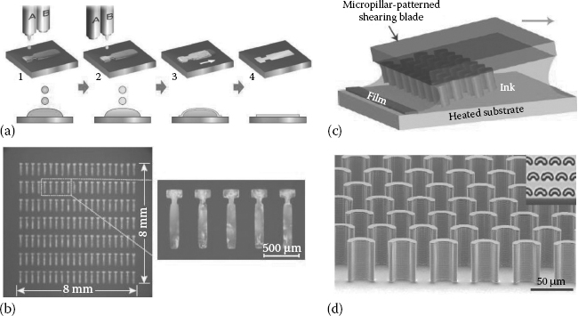
FIGURE 11.4 (See color insert) (a) Solution and (b) overview of a matrix of single crystals obtained with this technique. (c,d) Visual description of the solution-shearing method for originating solution-grown, oriented polycrystalline layers from drops of ink deposited onto substrates (c), and a scanning electron microscopic (SEM) image of the concave-shaped micropillar used for producing the needed shear stress in the deposited solution (d). (Reprinted by permission from Macmillan Publishers Ltd. [Nature] (From Minemawari, H., et al., 475, 364), copyright 2011; reprinted by permission from Macmillan Publishers Ltd. [Nature Materials] (Diao, Y., et al., 12, 665–671), copyright 2013.)
11.3 ORGANIC SEMICONDUCTING SINGLE-CRYSTAL PROPERTIES
In order to achieve the goal of low-cost organic electronics produced on a large scale [55,56,57,58,59,60], besides the need to find a convenient processing technique, a number of issues related to the charge transport in organic materials have to be clarified. When compared with inorganic semiconductors such as silicon or III–V compounds, it seems clear that technology based on organic semiconductors would vastly benefit from a much more systematic, basic understanding of the electronic properties of these materials. In particular, a clear and well-defined comprehension of their electronic behavior (including a complete description of the fundamental electronic states of the charge carriers) has still to be gained and related to their structural properties. In this respect, OSSCs provide a unique example of intrinsic electronic transport in organic materials, thanks to their long-range molecular order and to the limited charge-carrier trapping and hopping phenomena present in thin films, usually due to grain boundaries, interfaces, and structural imperfections. A useful investigation tool in this sense may be found in organic field-effect transistors (OFETs), which can provide precious information on the nature of the charge-transport phenomena in organic materials. Indeed, single-crystal organic transistors, in which the active channel is a single crystal, show the highest mobilities in organic materials, of several tens of cm2 V-1 s-1 [29,35,36,61], since a key parameter contributing to the mobility is the degree of molecular packing and the long-range order. Any process that modifies the molecular packing in the OSSC layer can affect the orbital overlap and therefore the transfer integral, which then affects charge-carrier mobilities. Several reviews have already discussed the chemical structure–molecular packing relationships for a variety of small-molecule OSSCs [62,63]. The methods employed for varying the molecular packing in a controlled way use chemical modifications of the OSSC or specific surface–OSSC interactions, such as the use of interfacial layers in the device-fabrication process or OSSC postprocessing conditions [64,65,66,67].
Nonetheless, the low symmetry of organic molecules leads to anisotropically packed crystal structures, which affects their transport properties (for example, the direction of the strongest p-orbital overlap usually coincides with the direction of the highest carrier mobility [4,28,29,30,35,68]). On the one hand, this asymmetry introduces difficulties for clearly understanding the transport behavior of the organic crystal, but on the other hand it offers the possibility of investigating the correlation between the three-dimensional molecular stacking order of OSSCs and their recently discovered anisotropic electronic transport properties. In particular, in recent years different mobilities have been measured along the three dimensions for micrometer- or nanometer-sized organic single crystals, either vapor deposited [4,28,29,30,35,68] or solution grown [43,51,53,50,69].
By means of space-charge-limited current (SCLC) [29,47,50,70] and by FET analyses [47,49], it is possible to carry out a complete characterization of several key electronic transport parameters of OSSCs.
We have recently reported on the electrical characterization of solution-grown, macroscopic 4HCB single crystals, and we will focus our attention on this specific crystal as a paradigm for OSSCs’ properties and applications.
In particular, we have determined (i) the majority carrier mobility, (ii) the density of states (DOS) distribution of the intrinsic electronic states, (iii) their concentration, and (iv) their energy levels in the bandgap. We provide evidence that all these properties are clearly anisotropic along the three crystal dimensions [49,50]. This anisotropicity of the electronic properties is due to the mentioned complex lattice structure of the 4HCB crystal (Figure 11.2), which was tentatively related to the transport properties by comparing the XRD-derived crystal structure with the three-dimensional anisotropic charge mobilities [47].
Figure 11.5 shows a sketch of the electrical contacts on the crystals, fabricated in alignment with the three main crystal axes and used to carry out the electrical characterization analyses aimed at correlating the crystal’s transport properties with its structural molecular packing.
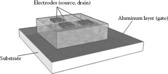
FIGURE 11.5 Layout of a 4HCB single crystal to be probed for anisotropic electronic properties. (From B. Fraboni, C. Femoni, I. Mencarelli, L. Setti, R. Di Pietro, A. Cavallini, A. Fraleoni-Morgera, Adv. Mater., 21, 1835, 2009; B. Fraboni, R. Di Pietro, A. Castaldini, A. Cavallini, A. Fraleoni-Morgera, L. Setti, I. Mencarelli, C. Femoni, Org. Electr., 9, 974, 2008.)
SCLC analyses carried out at room temperature allow the crystal’s electrical transport properties to be assessed and the charge-carrier mobility and the DOS distribution along the three axes to be determined [47,49,50] (Figure 11.6a). Photocurrent spectroscopy analyses allowed the effective electrical bandgap of 4HCB crystals to be determined, estimated at about 4 eV (Figure 11.6b).
Indeed, as shown in Figure 11.6a, the transport properties of 4HCB crystals reflect their anisotropic packing, and a clear difference in mobility values is found along the three axes. Charge-carrier mobilities of 0.1 cm2 V·s−1 can be easily and routinely obtained along the a axis of 4HCB solution-grown crystals, with very reproducible and stable results [50].
While the anisotropic electrical response of OSSCs is extremely interesting from the point of view of fundamental studies, it poses the problem of properly aligning the crystals and the electrodes in order to select and control the appropriate carrier-transport properties needed for specific device applications. Of course, proper determination of the crystallographic orientation of OSSCs is easily obtained via XRD, but this method has some limitations when applied to large arrays of crystals (as, for example, those shown in Figure 11.4b).
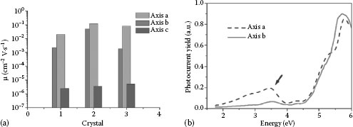
FIGURE 11.6 (a) Charge-mobility values determined from SCLC-based measurements in three different 4HCB single crystals along the three crystal axes, showing a remarkable reproducibility in each case. (b) Photocurrent yields along the two crystallographic axes a and b for a 4HCB single crystal. ((a) Reprinted from Org. Electr., 9, Fraboni, B., et al., 974. Copyright [2008], with permission from Elsevier; (b) reprinted from J. Cryst. Growth, 312, Fraleoni-Morgera, A., et al., 3466, Copyright [2010], with permission from Elsevier.)

FIGURE 11.7 (See color insert) Sketch of linearly polarized IR measurements carried out over 4HCB single crystals and the information achievable with this technique.
(Reproduced with permission from Fraleoni-Morgera, A., Tessarolo, M., Perucchi, A., Baldassarre, L., Lupi, S., Fraboni, B., J. Phys. Chem. C, 116, 2563. Copyright [2012] American Chemical Society.)
An effective way of assessing crystal orientation, more practical than XRD analyses for large numbers of crystals, is linearly polarized infrared spectroscopy (LP-IR). This technique has been demonstrated to be able to identify the crystallographic orientation due to the peculiar response of anisotropic crystals to linearly polarized radiation, allowing the crystal orientation to be clearly identified with no need for more intrusive and time-demanding XRD. In addition, LP-IR can be used to extract extremely useful fundamental information on the electrostatic intermolecular forces occurring within the crystal and possible molecular polarization phenomena, helping to understand the relations between the inner crystal structure and its electronic properties (Figure 11.7) [48,52].
11.4 X-RAY ELECTRICAL PHOTORESPONSE
The low dark current typical of organic semiconducting single crystals, their relatively good mobility, and the possibility of tuning their volume up to cubic millimeters with solution-growth techniques open up the possibility of using them as solid-state radiation detectors for x-rays.
We report here the main results observed on x-ray irradiation of 4HCB OSSCs. As shown in Figure 11.8a, a strong modification is induced in the current measured as a function of applied voltage along the vertical axis when a 4HCB crystal is exposed to an x-ray beam (35 keV, 170 mG s-1). A similar effect is visible along the planar axis (not reported here) [22].
Interestingly, the normalized photocurrent (ION–IOFF)/IOFF versus V curve presents a maximum at rather low voltages for both axes, suggesting that practical devices may be operated at voltages as low as a few tens of volts, hence with low power requirements (Figure 11.8b). The photoresponse has been measured on 4HCB crystals contacted with electrodes fabricated with different materials—a metal (Ag) and a conducting polymer (poly(ethylenedioxythiophene):poly(styrenesulfonate) [PEDOT:PSS])—to assess their charge-collecting properties and the crystal intrinsic response. The results, shown in Figure 11.8c for the vertical and planar axes, clearly indicate that highly reproducible and consistent results can be obtained with different types of electrodes.
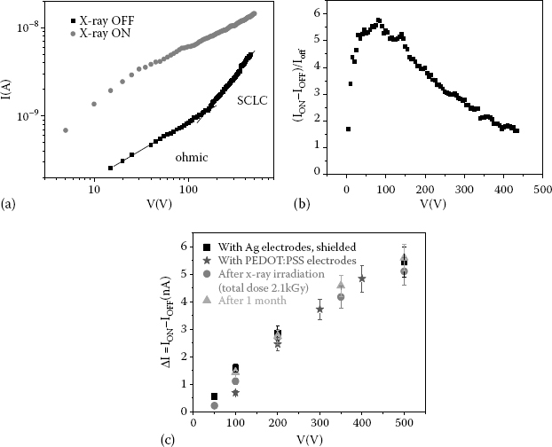
FIGURE 11.8 (See color insert) (a) Current–voltage curves for 4HCB-based devices in the dark (black squares) and under x-ray irradiation from a 35 keV Mo source at 170 mGy s−1 (red circles), for the vertical axis. Under x-ray irradiation, no ohmic–SCLC transition is detected along the vertical axis. (b) The maximum response can be achieved at low bias voltage (<100 V). (c) X-ray-induced current variation ΔI = (ION — IOFF) reported for different bias voltages applied to crystals contacted with Ag electrodes, before (black squares) and after irradiation with a total delivered x-ray dose of 2.1 kGy (red circles). The responses of crystals after an aging period of 1 month (blue triangles) and of crystals contacted with PEDOT:PSS electrodes (green stars) are also reported.
Thanks to these results, all-organic devices have been fabricated using a low-Z organic elastomer as a substrate (poly(dimethylsiloxane) [PDMS]) and a transparent and flexible conducting polymer (PEDOT:PSS) as electrode material. Such devices are composed of proven biocompatible materials and were found to be optically transparent and reasonably conformable (Figure 11.9), suggesting possible applications in bioelectronics.
The radiation hardness of these crystals is also quite remarkable. 4HCB-based devices were continuously exposed for 3 h to a 170 mGy s−1 dose rate (total dose of 2.1 kGy), and then tested under an x-ray beam that was switched on and off; after this rather high-dose irradiation, the devices’ electrical response to x-rays, ΔI, did not vary significantly; moreover, the same devices still provided a reliable response even after aging for 1 month (Figure 11.10). It is noteworthy that all the results reported here have been obtained in air and at room temperature, without any kind of encapsulation. Repeated x-ray-beam on/off cycles did not cause hysteresis or appreciable current drift at any of the bias voltages tested (Figure 11.10). The response time, shorter than 70 ms, is remarkably fast for organic electronic devices.
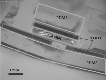
FIGURE 11.9 (See color insert) Optical microscopy image of a cross-sectional view of an optically transparent and bendable all-organic device with a 4HC crystal as the active sensing material. The PDMS substrate, the 4HCB crystal, and the PEDOT:PSS electrodes have been highlighted with color frames.
The response of 4HCB-based detectors is remarkably linear over quite a large range of dose rates (Figure 11.11a): the curves refer to the same single crystal probed along the vertical axis with two Ag electrodes and different applied bias. The fraction of e–h pairs collected at the electrodes following x-ray irradiation was evaluated using the measured photocurrent ΔI =(ION – IOFF). We estimated that about 5% of the impinging photons are absorbed within a typical crystal thickness of 600 μm by calculating the absorption coefficients to the Mo K lines (17.9 and 19.5 keV) with the XCOM code [71], and we estimated a minimum effective efficiency f ≈ 2%, which takes into account both the pair-production efficiency and the collection efficiency of the electrodes. These last two factors will have to be further improved to enhance the organic radiation-detector performance. To this end, future work in this field will focus on dedicated molecular-crystal engineering and device-geometry design and architectures. As a major example, the sensitivity, defined as S = ΔI/D, where D is the dose rate, can be significantly improved by simply improving the electrode geometry, and can reach up to 100 nC Gy-1 at 50 V (Figure 11.11b).
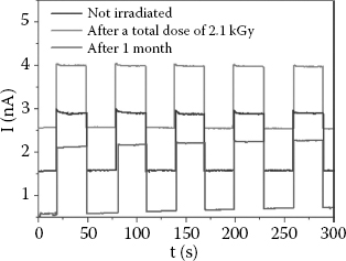
FIGURE 11.10 (See color insert) Electrical response of a 4HCB device to an on-off-switching x-ray beam at a bias voltage V = 100 V. The response is reported for an as-prepared device (black line) after it has been exposed for 3 h to a 170 mGy s−1 dose rate (total dose of 2.1 kGy) (red line) and after 1 month of storage in the ambient atmosphere (blue line).
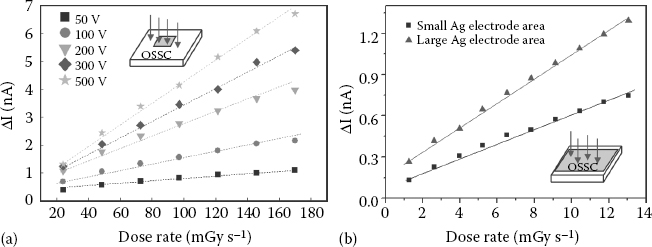
FIGURE 11.11 (See color insert) The x-ray-induced current variation ΔI =(ION – IOFF) is reported for increasing dose rates and different biases for the vertical axis of a 4HCB crystal on a quartz substrate with small-area (a) and large-area (b) Ag electrodes. (The lines are to guide the eye only.)
The organic single-crystal radiation detectors presented here allow x-rays to be detected directly; that is, the incoming x-ray photon is converted into an electrical signal. They provide a linear response to the x-ray dose rate, even for driving voltages as low as a few tens of volts, and they respond to an on/off-switching x-ray beam with no hysteresis effects. They are based on low-cost solution-grown organic molecular crystals (e.g., 4HCB and NTI) and can operate at room temperature, in air, and under ambient light with high reproducibility.
The observed behavior can be ascribed to the combination of different relevant properties of OSSCs: large bandgap, low dark current, good transport properties, ease of growth (by solution), dimension tenability, robust structure, and relatively low environment sensitivity.
4HCB-based detectors have been described in detail as an example, but other OSSCs present similar properties and provide a reliable response even after exposure to significant doses of x-ray irradiation and after being aged for up to 1 month. All-organic (i.e., not containing any high-Z compound), optically transparent x-ray detectors have been fabricated and demonstrated to be as effective, radiation hard, and linearly responsive as metal-containing ones. The overall performances of the devices presented here indicate that OSSCs are promising candidates for a new generation of direct electrical sensors for ionizing radiation, and the anisotropic electrical response of the molecular crystals can be exploited to develop unprecedented device architectures, possibly coupled to the conformable properties of all-organic devices.
As a future outlook, the possibility of directly growing single crystals from solution on a patterned substrate via ink-jet printing processes (see Section 11.2), coupled with the reported possibility of fabricating all-organic transparent radiation detectors (see Section 11.4), opens the way for the development of novel flexible sensor systems. Moreover, the low voltage required to operate OSSC detectors suggests that it might be possible to couple the radiation sensor to an organic electronic readout circuit, all printable on flexible substrates and operated at low bias voltages (typically <40 V if pentacene CMOS logic is employed). Breakthrough applications can be envisaged for this revolutionary sensing system, relevant in health diagnostics, in industrial process control, in citizen security and border control monitoring, and in wearable electronics.
The authors acknowledge financial support from the European Community under the FP7-ICT Project i-FLEXIS (2013–2016).
1. M. Berggren, A. Richter-Dalfors, Organic bioelectronics, Advanced Materials 2007, 19, 3201.
2. K. Müllen, U. Scherf, Organic Light-Emitting Devices: Synthesis, Properties and Applications, Wiley-VCH, Weinheim, Germany, 2006.
3. T. Sekitani, U. Zschieschang, H. Klauk, T. Someya, Flexible organic transistors and circuits with extreme bending stability, Nature Materials 2009, 9, 1015.
4. C. Reese, Z. Bao, Organic single-crystal field-effect transistors, Materials Today 2007, 10, 20.
5. S. Gunes, H. Neugebauer, N. Sariciftci, Conjugated polymer-based organic solar cells, Chemical Reviews 2007, 107, 1324.
6. R. Capelli et al., Organic light-emitting transistors with an efficiency that outperforms the equivalent light-emitting diodes, Nature Materials 2010, 9, 496.
7. E. Roeling, et al. Organic electronic ratchets doing work, Nature Materials 2011, 10, 51.
8. L. Christophorou, J. Carter, Improved organic scintillators in 2-ethyl naphthalene, Nature 1966, 212, 816.
9. G. Hull, N. Zaitseva, N. Cherepy, J. Newby, W. Stoeffl, S. Payne, New organic crystals for pulse shape discrimination, IEEE Transactions on Nuclear Science 2009, 56, 899.
10. P. Keivanidis, N. Greenham, H. Sirringhaus, R. Friend, J. Blakesley, R. Speller, M. Campoy-Quiles, T. Agostinelli, D. Bradley, J. Nelson, x-ray stability and response of polymeric photodiodes for imaging applications, Applied Physics Letters 2008, 92, 23304.
11. T. Agostinelli, M. Campoy-Quiles, J. Blakesley, R. Speller, D. Bradley, J. Nelson, A polymer/fullerene based photodetector with extremely low dark current for x-ray medical imaging applications, Applied Physics Letters 2008, 93, 203305.
12. S. Tedde, J. Kern, T. Sterzl, J. Fürst, P. Lugli, O. Hayden, Fully spray coated organic photodiodes, Nano Letters 2009, 9, 980.
13. R. Newman, H. Sirringhaus, J. Blakesley, R. Speller, Stability of polymeric thin film transistors for x-ray imaging applications, Applied Physics Letters 2007, 91, 142105.
14. M. Atreya et al., Stability studies of poly(2-methoxy-5-(2’-ethyl hexyloxy)-p-(phenylene vinylene) [MEH-PPV], Polymer Degradation and Stability 1999, 65, 287.
15. E. Silva, J. Borin, P. Nicolucci, C. Graeff, T. Ghilardi Netto, R. Bianchi, Low dose ionizing radiation detection using conjugated polymers, Applied Physics Letters 2005, 86, 131902.
16. L. Zuppiroli, S. Bouffard, J. Jacob, Ionizing radiation dosimetry in the absorbed dose range 0.01–50 MGy based on resistance and ESR linewidth measurements of organic conducting crystals, International Journal of Applied Radiation and Isotopes 1985, 36, 843.
17. S. Graham, R. Friend, S. Fung, S. Moratti, High sensitivity radiation sensing by photo induced doping in PPV derivatives, Synthetic Metals 1987, 84, 903.
18. P. Beckerle, H. Ströbele, Charged particle detection in organic semiconductors, Nuclear Instruments and Methods in Physics Research Section A 2000, 449, 302.
19. F. Boroumand, M. Zhu, A. Dalton, J. Keddie, P. Sellin, J. Gutierrez, Direct x-ray detection with conjugated polymer devices, Applied Physics Letters 2007, 91, 33509.
20. A. Intaniwet, J. Keddie, M. Shkunov, P. Sellin, High charge-carrier mobilities in blends of poly(triarylamine) and TIPS-pentacene leading to better performing x-ray sensors, Organic Electronics 2011, 12, 1903.
21. A. Intaniwet, C. Mills, M. Shkunov, P.J. Sellin, J.L. Keddie, High-Z nanoparticles for enhanced sensitivity in semiconducting polymer x-ray detectors, Nanotechnology 2012, 23, 235502.
22. B. Fraboni, A. Ciavatti, F. Merlo, L. Pasquini, A. Cavallini, A. Quaranta, A. Bonfiglio, A. Fraleoni-Morgera, Organic semiconducting single crystals as next generation of low-cost, room-temperature electrical x-ray detector, Advanced Materials 2012, 24, 2289.
23. A. Ohtomo, H. Hwang, A high-mobility electron gas at the LaAlO3/SrTiO3 heterointerface, Nature 2004, 427, 4236.
24. A. Tsukazaki, et al., Observation of the fractional quantum Hall effect in an oxide, Nature Materials 2010, 9, 889.
25. J. Takeya, et al., Very high-mobility organic single-crystal transistors with in-crystal conduction channels, Applied Physics Letters 2007, 90, 102120.
26. A. Briseno, et al., Patterning organic single-crystal transistor arrays, Nature 2006, 444, 913.
27. N. Karl, Charge carrier transport in organic semiconductors, Synthetic Metals 2002, 649, 133.
28. V. Sundar, et al., Elastomeric transistor stamps: Reversible probing of charge transport in organic crystals, Science 2004, 303, 1644.
29. de Boer, et al., Organic single-crystal field-effect transistors, Physica Status Solidi A 2004, 201, 1302.
30. H. Yan, Z.H. Chen, Y. Zheng, C. Newman, J.R. Quinn, F. Dotz, M. Kastler, A. Facchetti, A high-mobility electron-transporting polymer for printed transistors, Nature 2009, 457, 679.
31. V. Podzorov, E. Menard, A. Borissov, V. Kiryukhin, J.A. Rogers, M.E. Gershenson, Intrinsic charge transport on the surface of organic semiconductors, Physics Review Letters 2004, 93, 086602.
32. H.Y. Li, B.C.K. Tee, J.J. Cha, Y. Cui, J.W. Chung, S.Y. Lee, Z.N. Bao, High-mobility field-effect transistors from large-area solution-grown aligned C60 single crystals, Journal of the American Chemical Society 2012, 134, 2760.
33. A.L. Briseno, et al., Patterning organic single-crystal transistor arrays, Advanced Materials 2006, 18, 2320–2324.
34. N. Karl, Growth and electrical properties of high purity organic molecular crystals, Journal of Crystal Growth 1990, 99, 1009–1016.
35. R. Zeis, C. Besnard, T. Siegrist, C. Schlockermann, X. Chi, C. Kloc, Field effect studies on rubrene and impurities of rubrene, Chemistry of Materials 2006, 18, 24.
36. O.D. Jurchescu, J. Baas, T.T.M. Palstra, Effect of impurities on the mobility of single crystal pentacene, Applied Physics Letters 2004, 84, 3061.
37. G. Müller, J.-J. Métois, P. Rudolph (eds), Crystal Growth—From Fundamentals to Technology, 2004, Elsevier, Amsterdam.
38. M. Arivanandhan, K. Sankaranarayanan, P. Ramasamy, Melt growth of novel organic nonlinear optical material and its characterization, Materials Letters 2007, 61, 4836.
39. K. Sankaranarayanan, P. Ramasamy, Unidirectional crystallization of large diameter benzophenone single crystal from solution at ambient temperature, Journal of Crystal Growth 2006, 292, 445.
40. N. Vijayan, R. Ramesh Babu, M. Gunasekaran, R. Gopalakrishnan, R. Kumaresan, P. Ramasamy, C.W. Lan, Studies on the growth and characterization of p-hydroxyaceto-phenone single crystals, Journal of Crystal Growth 2003, 249, 309–315.
41. S. Janarthanan, R. Sugaraj Samuel, S. Selvakumar, Y.C. Rajan, D. Jayaraman, S. Pandi, Growth and characterization of organic NLO crystal: ß-Naphthol, Journal of Materials Science and Technology 2011, 27, 271.
42. R. Li, W. Hu, Y. Liu, D. Zhu, Micro- and nanocrystals of organic semiconductors, Accounts of Chemical Research 2010, 43, 529.
43. S.C.B. Mannsfeld, A. Sharei, S. Liu, M.E. Roberts, I. McCulloch, M. Heeney, Z. Bao, Highly efficient patterning of organic single-crystal transistors from the solution phase, Advanced Materials 2008, 20, 4044.
44. N. P. Zaitseva et al., Neutron detection with single crystal organic scintillators, Proceedings of SPIE 2009, 744911, 744911-(1–10).
45. G. Hull et al., New organic crystals for pulse shape discrimination, IEEE Transactions on Nuclear Science 2009, 56, 899.
46. S.K. Park, T.N. Jackson, J.E. Anthony, D.A. Mourey, High mobility solution processed 6,13-bis(triisopropyl-silylethynyl) pentacene organic thin film transistors, Applied Physics Letters 2007, 91, 063514.
47. B. Fraboni, C. Femoni, I. Mencarelli, L. Setti, R. Di Pietro, A. Cavallini, A. Fraleoni-Morgera, Solution-grown, macroscopic organic single crystals exhibiting three-dimensional anisotropic charge-transport properties, Advanced Materials 2009, 21, 1835.
48. E. Capria, L. Benevoli, A. Perucchi, B. Fraboni, M. Tessarolo, S. Lupi, A. Fraleoni-Morgera, Infrared investigations of 4-hydroxycyanobenzene single crystals, Journal of Physical Chemistry A 2013, 117, 6781.
49. B. Fraboni, R. Di Pietro, A. Castaldini, A. Cavallini, A. Fraleoni-Morgera, L. Setti, I. Mencarelli, C. Femoni, Anisotropic charge transport in organic single crystals based on dipolar molecules, Organic Electronics 2008, 9, 974.
50. B. Fraboni, A. Fraleoni-Morgera, A. Cavallini, Three-dimensional anisotropic density of states distribution and intrinsic-like mobility in organic single crystals, Organic Electronics 2010, 11, 10.
51. A. Fraleoni-Morgera, L. Benevoli, B. Fraboni, Solution growth of single crystals of 4-hydroxycyanobenzene (4HCB) suitable for electronic applications, Journal of Crystal Growth 2010, 312, 3466.
52. A. Fraleoni-Morgera, M. Tessarolo, A. Perucchi, L. Baldassarre, S. Lupi, B. Fraboni, Polarized infrared studies on charge transport in 4-hydroxycyanobenzene single crystals, Journal of Physical Chemistry C 2012, 116, 2563.
53. H. Minemawari, T. Yamada, H. Matsui, J. Tsutsumi, S. Haas, R. Chiba, R. Kumai, T. Hasegawa, Inkjet printing of single-crystal films, Nature, 2011, 475, 364.
54. Y. Diao, B.C.-K. Tee, G. Giri, J. Xu, D.H. Kim, H.A. Becerril, R.M. Stoltenberg, T.H. Lee, G. Xue, S.C.B. Mannsfeld, Z. Bao, Solution coating of large-area organic semiconductor thin films with aligned single-crystalline domains, Nature Materials 2013, 12, 665–671.
55. A. Dodabalapour, Organic and polymer transistors for electronics, Materials Today 2006, 9, 24.
56. C. Brabec, Organic photovoltaics: Technology and market, Solar Energy Materials and Solar Cells 2004, 83, 273.
57. B. Geffro, P. le Roy, C. Prat, Organic light-emitting diode (OLED) technology: Materials, devices and display technologies, Polymer International 2006, 55, 572.
58. A. Misra, P. Kumar, M. Kamalasanan, C. Chandra, White organic LEDs and their recent advancements, Semiconductor Science and Technology 2006, 21, R35.
59. T. Kawanishi et al., High-mobility organic single crystal transistors with submicrometer channels, Applied Physics Letters 2008, 93, 23303.
60. H. Alves, E. Molinari, H. Xie, A. Morpurgo, Metallic conduction at organic chargetransfer interfaces, Nature Materials 2008, 7, 574.
61. H. Li, G. Giri, J.B.-H. Tok, Z. Bao, Toward high-mobility organic field-effect transistors: Control of molecular packing and large-area fabrication of single-crystal-based devices, MRS Bulletin 2013, 38, 42.
62. M.L. Tang, J.H. Oh, A.D. Reichardt, Z.N. Bao, Chlorination: A general route toward electron transport in organic semiconductors, Journal of the American Chemical Society 2009, 131, 3733.
63. J.E. Anthony, A. Facchetti, M. Heeney, S.R. Marder, X. Zhan, n-type organic semiconductors in organic electronics, Advanced Materials 2010, 22, 3876.
64. B.J. Jung, N.J. Tremblay, M.L. Yeh, H.E. Katz, Molecular design and synthetic approaches to electron-transporting organic transistor semiconductors, Chemistry of Materials 2011, 23, 568
65. J.H. Oh, S.L. Suraru, W.Y. Lee, M. Konemann, H.W. Hoffken, C. Roger, R. Schmidt, Y. Chung, W.C. Chen, F. Wurthner, Z.N. Bao, High-performance air-stable n-type organic transistors based on core-chlorinated naphthalene tetracarboxylic diimides, Advanced Functional Materials 2010, 20, 2148.
66. K.P. Goetz, Z. Li, J.W. Ward, C. Bougher, J. Rivnay, J. Smith, B.R. Conrad, S.R. Parkin, T.D. Anthopoulos, A. Salleo, J.E. Anthony, O.D. Jurchescu, Effect of acene length on electronic properties in 5-, 6-, and 7-ringed heteroacenes, Advanced Materials 2011, 23, 3698.
67. J.K. Takimiya, S. Shinamura, I. Osaka, E. Miyazaki, Thienoacene-based organic semiconductors, Advanced Materials 2011, 23, 4347.
68. J. Lee, S. Roth, Y. Park, Anisotropic field effect mobility in single crystal pentacene, Applied Physics Letters 2006, 88, 25216.
69. Q. Tang, et al., Micrometer- and nanometer-sized organic single-crystalline transistors, Advanced Materials 2008, 20, 2947.
70. D. Braga, N. Battaglini, A. Yassar, G. Horowitz, M. Campione, A. Sassella, A. Borghesi, Bulk electrical properties of rubrene single crystals: Measurements and analysis, Physical Review B 2008, 77, 115205.
71. M.J. Berger, et al., XCOM: Photon cross sections database. NBSIR 87-3597. National Institute of Standards and Technology. http://www.nist.gov/pml/data/xcom/index.cfm.