
CONTENTS
7.2 Calibration of Hybrid Pixel Detectors
7.2.2.1 Energy Calibration of Analog Threshold
7.2.2.2 Energy Calibration of Time over Threshold Mode
7.3 Performance and Limitations
7.4 Characterization of Hybrid Pixel Detectors
7.4.1 Practical Considerations
7.4.2 Characterization of CdTe Sensors Bump Bonded to Hybrid Pixel Detectors
7.4.2.2 Verification of the Sensitive Volume and Depth-of-Interaction Effects
7.4.2.3 Electrical Field Distortions around “Blob” Defects
7.5 Outlook and Future Challenges
This chapter will introduce the concept of single photon processing hybrid pixel detectors before moving on to characterize hybrid pixel detectors using synchrotron radiation and in particular monoenergetic pencil beams. The focus will be on the sensor side and especially cadmium telluride (CdTe) sensors with small pixels, but application-specific integrated circuit (ASIC) aspects will also be covered. A monochromatic pencil beam is a very useful tool for detector characterization since both the position and the amount of energy deposited are then known. Together with a hybrid pixel detector that can resolve the response from a single photon, effects in the sensor layer can be studied in detail. The fine segmentation, down to 55 μm, also gives the ability to map how parameters change over the area and, in combination with a titled beam, it is possible to generate a three-dimensional (3-D) map over the sensor volume.
Most of the measurements in this chapter have been performed with the Timepix [1] or the Medipix3RX [2] chip and therefore an introduction to these detectors is included. Methods and results can, however, be generalized to other detector systems.
A hybrid pixel detector consists of two layers, a sensor layer and an electronics layer as shown in Figure 7.1. The advantages of this detector are that the different layers can be optimized for a specific application ex. using a high-Z sensor material to increase x-ray photon absorption and that there is no dead area where the electronics are situated as in monolithic sensors. However, each pixel in the sensor layer must be connected to the corresponding pixel in the read-out layer thus adding a complex processing step and increasing the cost. For particle physics applications, the extra electronics layer and the bump bonds also add extra material causing the particles to scatter. Due to their high performance, hybrid pixel detectors are still preferred over monolithic sensors.
The pixel pitch varies between applications and detectors ranging from approximately 0.25–1 mm for medical computed tomography (CT) detectors [3] to about 50–100 μm for state-of-the-art multipurpose photon counting (PC) chips [1,2,4,5,6] down to 25 μm for the newest prototypes [7].
The Timepix [1] chip is a hybrid pixel detector developed in the framework of the Medipix2 collaboration [8]. The pixel matrix consists of 256 × 256 pixels with a pitch of 55 μm, which gives a sensitive area of about 14 × 14 mm2. Timepix is designed in a 0.25 μm complementary metal–oxide–semiconductor (CMOS) process and has about 500 transistors per pixel (Figure 7.2).

FIGURE 7.1 Schematic of a hybrid pixel detector.

FIGURE 7.2 Timepix chip with a 1 mm thick CdTe sensor.
The chip has one analog threshold and it can be operated in PC, time over threshold (ToT), or time of arrival (ToA) mode. The principles of the different operating modes are shown in Figure 7.3. In the PC mode, the counter is incremented once for each pulse that is over the threshold, while in the ToT mode the counter is incremented as long as the pulse is over the threshold, and in the ToA mode the pixel starts to count when the signal crosses the threshold and keeps counting until the shutter is closed. In the measurements described, only the PC and the ToT modes have been used but the ToA mode is very useful and has applications in mass spectrometry [9,10] and particle tracking [11] among other areas.
While Timepix is a general-purpose chip, the Medipix3RX [2] is much more aimed at x-ray imaging. It can be configured with up to eight analog thresholds per pixel and features analog charge summing over dynamically allocated 2 × 2 pixel clusters. The intrinsic pixel pitch of the ASIC is 55 μm and if bump bonded in this mode, which is called the fine pitch mode, the chip can then be run with either four thresholds per pixel in single pixel mode or with two thresholds per pixel in charge summing mode. Optionally, the chip can be bump bonded with a 110 μm pitch then combining counters and thresholds from four pixels. Operation is then possible in single pixel mode with eight thresholds per pixel or in charge summing mode having four thresholds and a summing charge of 220 × 220 μm2 in area.
As the Medipix3RX is a very versatile and configurable chip there is also a possibility to utilize the two counters per pixel and run in continuous read/write mode where one counter counts while the other one is being read out. This eliminates the read-out dead time but comes at the cost of losing one threshold since both counters need to be used for the same threshold.
The charge summing mode is a very important feature to combat contrast degradation by charge sharing in hybrid pixel detectors with small pixels. The effect of the charge summing mode is showed in Figure 7.4 where it is compared with the single pixel mode for a Medipix3RX chip illuminated by 10 keV photons at the ANKA synchrotron. In this case, the sensor was a 300 μm thick p-on-n silicon sensor with a 55 μm pixel pitch.

FIGURE 7.3 Schematic of the three different operating modes in the Timepix chip showing (a) the signal after the preamplifier, (b) the response in photon counting mode where each pulse is counted once, (c) response in time over threshold mode where the length of the pulse (in clock cycles) is counted, and (d) time of arrival mode where the counter starts counting when the pulse goes over the threshold and then counts until the shutter is closed.
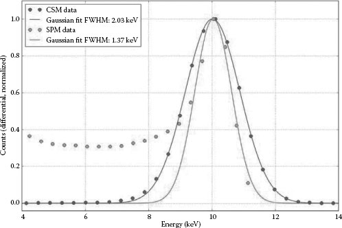
FIGURE 7.4 Comparison between the single pixel mode and the charge summing mode of Medipix3RX.
7.2 CALIBRATION OF HYBRID PIXEL DETECTORS
Before calibrating a hybrid pixel detector, the chip has to be equalized in order to minimize the threshold dispersion between pixels. This is because the threshold that the pixel sees is applied globally but the zero level of the pixel can be slightly different due to process variations affecting the baseline of the preamplifier.
The equalization is done with a threshold adjustment digital-to-analog converter (DAC) in each pixel. The resolution of the adjustment DAC is usually in the range of 4 bits as in the Timepix to 6 bits as in the Eiger chip [6]. The standard way to calculate the adjustment setting for each pixel is by scanning the threshold and finding the edge of the noise, then aligning the noise edges. This adjusts correctly for the zero level of the pixel but gain variations can still deteriorate the energy resolution at a given energy. To correct for the gain mismatch, either test pulses or monochromatic x-ray radiation has to be used for the equalization, thereby equalizing at the energy of interest instead of the zero level. In Figure 7.5 the threshold dispersion before equalization and after equalization with both noise and test pulses is shown for the Medipix3RX chip. A method for the equalization and calibration of the Eiger chip using monochromatic x-ray radiation at several energies can be found in a paper by Kraft et al. [12].
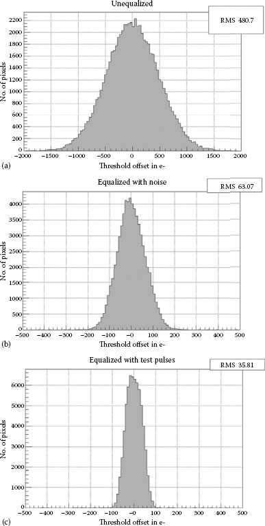
FIGURE 7.5 Threshold dispersion at (a) noise level before equalization and at 8 keV after (b) noise and (c) test pulse equalization for the Medipix3RX chip in single pixel super high gain mode. Note the different scales on the x-axis.
Depending on the chip, two types of energy calibration are necessary: calibration of the analog threshold and calibration of the ToT response. For a strictly PC chip such as Medipix3RX, Pixirad, or Eiger, the only calibration is the calibration of the analog threshold, whereas in a ToT measuring chip, such as Timepix and Clicpix, the ToT response has to be calibrated as well.
7.2.2.1 Energy Calibration of Analog Threshold
To calibrate the threshold, monochromatic photons or at least radiation with a pronounced peak is required. These can be obtained from radioactive sources, by x-ray fluorescence, or from synchrotron radiation. To find the corresponding energy for a certain threshold, the threshold is scanned over the range of the peak and an integrated spectrum or S-curve is obtained. The data are then either directly fitted with an error or sigmoid function or are first differentiated and then fitted with a Gaussian function. From this fit, the peak position and the energy resolution can be extracted. Repeating the procedure for multiple peaks, the result can then be fitted with a linear function and the relation between the threshold setting in DAC steps or millivolts (mV) and the deposited energy in the sensor can be found. A calibration of a Medipix3RX chip in charge summing mode is shown in Figure 7.6 with the corresponding information on the fluorescence peak that was used to generate the radiation.
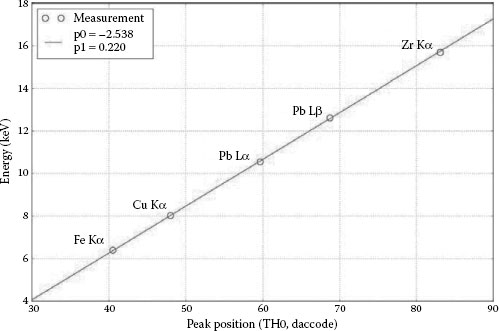
FIGURE 7.6 Energy calibration of a Medipix3RX chip in charge summing mode. The labels show the corresponding fluorescence peak used and p0 and p1 are the coefficients for the linear fit.
7.2.2.2 Energy Calibration of Time over Threshold Mode
For detectors with the ToT capability, for example the Timepix, the ToT response also has to be calibrated. This is slightly more difficult since the ToT to energy relation is not linear but rather a surrogate function. This is because while the amplitude of the pulse is proportional to the energy of the incoming photon, the length of the pulse deviates from linear behavior at low pulse heights due to the shape of the pulse. Equation 7.1 shows the relation between ToT, f(x), and the energy of the incoming photon, x. The equation is taken from [13], where Jan Jakubek presents a calibration procedure for the Timepix chip.
(7.1) |
In Figure 7.7, the fitted calibration function for several pixels is plotted and in Figure 7.8 the energy spectrum from a 241Am source is shown before and after calibration for a few pixels in the detector. This highlights the importance of per-pixel calibration to achieve an optimal energy response.
7.3 PERFORMANCE AND LIMITATIONS
Single photon processing hybrid pixel detectors offer excellent performance; however, it is important to understand the applications and the limitations of the current detectors. By applying a threshold and counting each photon, the noise from integrating the leakage current seen in charge-integrating devices is removed. This is especially important in low-flux measurements where the signal could be completely drowned in noise.

FIGURE 7.7 (See color insert) Calibration functions for several pixels in a Dosepix chip.

FIGURE 7.8 (See color insert) Measured photon energy spectrum for a 241Am source for a few pixels in a Dosepix detector before and after calibration.
Also looking at the contrast-to-noise ratio, in a charge-integrating device the photons are weighted according to their energy, W ∝ E, which means that for a low-contrast imaging task the high-energy photons will mask the more important low-energy photons. A study by Giersch et al. [14] has shown that the signal-to-noise ratio in a low-contrast imaging task such as mammography CT can be increased by 30% by using PC, thus weighting photons W = 1 by 90% by introducing optimal weighting where each photon is weighted by W ∝ E−3.
To minimize the dose to the patient, a high quantum efficiency is very important in medical imaging. To this end, there is a need to move away from silicon because although it is a very well understood material and is available in excellent quality, its atomic number is too low to reach a high efficiency. Figure 7.9 shows the x-ray absorption for silicon (Si), gallium arsenide (GaAs), and CdTe of 1 mm thickness up to 140 keV, which are the three main candidates for x-ray imaging applications. GaAs for medium energies and CdTe/cadmium zinc telluride (CdZnTe) for high energies. Both materials still have their problems, such as point defects and trapping, but their quality is improving. Later in the chapter, the properties of CdTe will be more closely examined and its defects will be characterized.
An intrinsic problem with all high-Z sensor materials is x-ray fluorescence. When a primary photon is absorbed, an electron in the atom is excited and the atom then emits a fluorescence photon as it is de-excited. The range of this photon depends on the material and the electron layer containing the excited electron. Both the range and the yield of the fluorescence photons increase with the atomic number of the material. In GaAs, the fluorescence photons have a mean free path of 16 and 40 μm, respectively, and in CdTe the ranges are 120 and 60 μm for the Kα photons.

FIGURE 7.9 X-ray absorption for a 1 mm thick sensor of Si, GaAs, and CdTe. (Generated with XOP2.3 [15].)
If the distance that the fluorescence photon can travel is comparable or larger than the pixel pitch, this will lead to a degradation of the energy response and a blurring of the picture. This can, to some extent, be corrected for by charge summing, either in the ASCI as for the Medipix3RX or off-line provided that the energy and time information are available from, for example, ToT measurements with Timepix. However, one portion of the fluorescent photons will always escape from the sensor volume and therefore will not be corrected for.
When the pixel size starts to approach the size of the charge cloud, the signal from more and more photons is subjected to charge sharing. Charge sharing creates a characteristic low-energy tail and leads to a reduced contrast and distorted spectral information. To counteract this problem there are two possibilities, either to use larger pixels and then reduce the spatial resolution or to implement charge summing on a photon-by-photon basis.
For lower rates and with detectors that store the energy information in each pixel, using either ToT such as Timepix or a peak-and-hold circuit and an ADC such as Hexitec [16] the charge summing can be done off-line. This requires, however, that a second hit does not occur in the same pixel before the read out. Using this approach, charge that is below the threshold is lost.
Another approach is to sum the charge in the detector as implemented in Medipix3RX, where the analog charge is summed in a 2 × 2 cluster before being compared with the threshold. The advantage of this approach is that it can handle much higher interaction rates and also that even charge below the threshold is summed as long as one pixel is triggered. However, since this has to be implemented in the ASIC, it complicates the design and is less flexible. There is also a practical limit to how many pixels over which the summation can be done. The importance of charge summing when using thick sensors with small pixels is highlighted by Figure 7.10 where the energy response of a 2 mm thick CdTe sensor with 110 μm pixels bump bonded to Medipix3RX is shown both in single pixel mode and in charge summing mode.
Given that the processing of each photon takes a finite time, during high interaction rates there will be problems with pileup especially for medical CT where the photon flux can reach 109 photons mm−2 s−2 in the direct beam. This is caused when a second photon arrives in the same pixel before the first photon is processed. Depending on the detector, the second photon could either be lost or added to the signal of the first photon. The result will be a deviation from linear behavior for the count rate as shown in Figure 7.11. This can, however, be corrected for up to a certain limit, but more problematic is the spectral distortion as an effect of pileup, which is an effect that cannot be easily corrected for.

FIGURE 7.10 Energy response of a 2 mm thick CdTe sensor with 110 μm pixels bump bonded to Medipix3RX in both single pixel mode and charge summing mode (CSM). The source is x-ray fluorescence from praseodymium. Kα and Kβ lines are visible but not clearly resolved.
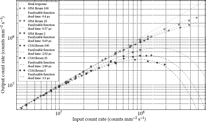
FIGURE 7.11 (See color insert) Count-rate behavior for Medipix3RX in single pixel mode (SPM) and charge summing mode (CSM) for different settings.
Different detectors will have different responses and it is important that the detector used is characterized and suitable for the flux in a specific application. Since the flux is measured per area, smaller pixels are an advantage leading to less photons per second per pixel.
7.4 CHARACTERIZATION OF HYBRID PIXEL DETECTORS
Many synchrotron facilities offer microfocused pencil beams, with a beam size in the range of a few microns. This section describes practical considerations for the setup and information gained from the tests available.
7.4.1 PRACTICAL CONSIDERATIONS
In an effort to combine high spatial resolution with high quantum efficiency many hybrid pixel detectors use a small pixel pitch combined with a thick sensor. For example, both 55 and 110 μm pixel pitches with a 1 mm thick sensor have been tested with Timepix [17] and recently a 110 μm pixel pitch with a 2 mm thick sensor was used with Medipix3RX [18]. Another detector, Pixirad, uses a 60 μm pitch with 650 μm thick sensors [5]. An aspect ratio, in the range of 1:10–1:20, puts very high demands on the alignment of the sensor in respect of the incoming beam because even a slight misalignment would illuminate several pixels and distort the results as shown in Figure 7.12.
For simplicity, the rotation of a sensor in respect of a perfectly aligned sensor with a horizontal x-axis, a vertical y-axis, and a z-axis in the beam direction will be defined, as shown in Figure 7.13. In order to align the sensor, a small visible laser is installed at the beamline. The laser is aimed in the direction of the beam and the reflection of the laser spot of the sensor back to the laser is used for alignment. A large distance of, for example, 4 m, and a small spot in size guarantees that when the reflected spot hits the laser there is a very small rotation around either the x- or y-axis. Assuming that, using only the eye, the spot can be aligned with the laser to a 1 mm precision, then the biggest rotation possible is 0.014°, which could at most have the beam moving 0.25 μm in x or y while traversing a 1 mm thick sensor.
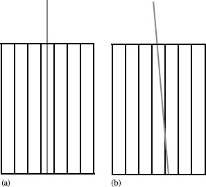
FIGURE 7.12 (a) Good alignment and (b) the effects of a 5° misalignment with a 1:10 aspect ratio.
The alignment of the rotation around the z-axis is then done by positioning the beam in the center of one pixel at the edge of the chip and then moving it to the other side of the chip. This will reveal any rotation around the z-axis. Because of the charge sharing in the sensors used, a movement significantly smaller than one pixel can be determined.
The beams produced by synchrotrons are generally very clean and have excellent energy resolution. However, for some of the tests with hybrid pixel detectors, the beam has to be strongly attenuated using aluminum filters to be able to resolve individual photons. This causes beam hardening since the lower energies are attenuated more than the higher energies. As an example, in calculating the intensities of a 10 keV primary beam and a 30 keV second harmonic passing through a 2 mm aluminum filter, the primary beam is attenuated 150 times more than the harmonic.
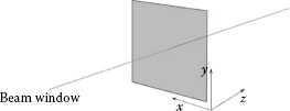
FIGURE 7.13 Sensor orientation.
So, after attenuation, otherwise nonvisible higher-order harmonics of a crystal monochromator might become visible. Figure 7.14 shows a range of harmonics measured with the Medipix3RX chip at B16 and Figure 7.15 shows the attenuation of a 25 keV tilted beam passing through a CdTe sensor bonded to a Timepix chip. With the tilted beam the signal is expected to decrease exponentially (a straight line in log scale) but the plot shows two different slopes, indicating that the primary 25 keV beam dominates in the upper layers and the second harmonic at 75 keV dominates in the lower layers.
The actual amount of harmonics in the beam will vary between beamlines and depends strongly on the filtration but it is something that has to be considered when planning and analyzing a measurement.
7.4.2 CHARACTERIZATION OF CDTE SENSORS BUMP BONDED TO HYBRID PIXEL DETECTORS
To show the types of measurements possible and also report on the results of a new CdTe sensor with very small pixels, this section will go through the measurements performed on sensors with a 55 and 110 μm pixel pitch bump bonded to the Timepix ASIC. Both sensors were 1 mm thick. The CdTe used was grown by ACRORAD [19] using the traveling heater method and processing and hybridization was done at FMF Freiburg. To prevent the material properties from deteriorating, a low-temperature solder process was used. Contacts were intentionally ohmic, which should lead to less polarization and also offers the possibility to operate the same detector in either electron or hole collection mode, which is interesting when characterizing the material.

FIGURE 7.14 Integrated spectrum measured with Medipix3RX showing several harmonics. Monochromator set to 10 keV.
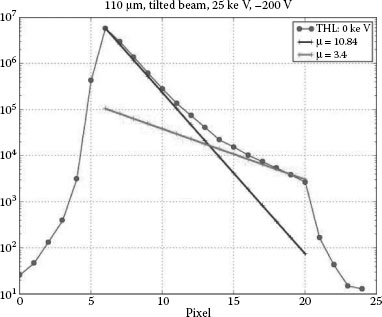
FIGURE 7.15 Attenuation during transmission of a 25 keV pencil beam at 30° through a CdTe sensor.
The μτ product was measured by Greiffenberg et al. [17] to be μeτe = (1.9 ± 0.6)10−3 cm2 V−1 and μhτh = (0.75 ± 0.25)10−4 cm2 V−1 for electrons and holes, respectively, using a particles. The possibility of collecting both electrons and holes is of course essential in this case and having a pixellated ASIC allows for a two-dimensional (2-D) map of the transport properties using a standard 241Am laboratory source.
7.4.2.2 Verification of the Sensitive Volume and Depth-of-Interaction Effects
The depth-of-interaction dependence in the 1 mm thick CdTe sensor with a pixel pitch of 110 μm was investigated at the I15 Beamline at Diamond Light Source [20]. To do this, the sensor was illuminated with a 77 keV monochromatic pencil beam at an angle of 20° to the sensor surface. This meant that the beam passed through 25 pixels before exiting the sensor. First, to verify that the detector was working well and to verify the sensitivity of the whole volume and that there was no problem with the beam, an absorption profile was measured in PC mode. Then, to measure the energy response the Timepix chip was used in ToT mode and spectra were generated for each pixel thus representing a different depth in the sensor. For both of these measurements, the sensor was biased at −300 V to collect electrons.
Figure 7.16 presents the results at 20° and 25°. Much valuable information can be extracted from the plot. It shows that the detector is working correctly throughout the full thickness covering more than three orders of magnitude in count rate, which is expected but nevertheless an important confirmation. Since the y-axis is in logarithmic scale, the straight line of the profile confirms that the incoming beam is dominated by a single energy and the extracted linear attenuation coefficient is consistent with CdTe and 77 keV. Furthermore, having two different angles with a well-known difference between them (given by the rotation stage), it is possible to calculate the absolute angle and verify the alignment.

FIGURE 7.16 Absorption profile of a 77 keV pencil beam at 20° and 25° to the sensor surface.
To investigate the material performance, a good area of the chip was chosen to eliminate the influence from localized defects. Analyzing interactions from individual photons it was also possible to look at the diffusion at different depths and the influence of fluorescence. To minimize the effects of trapping, the sensor was used in electron collection mode, which is the normal way to operate CdTe sensors.
In Figure 7.17, no depth-of-interaction effect is visible even for the lowest layer measured. This is consistent with a signal that is generated very close to the pixel and is completely dominated by electrons as the “small pixel effect” [21] for a detector W/L = 0.11 would predict. This also shows that the trapping of electrons is sufficiently low not to affect the signal on a level that can be measured with the Timepix chip in a 1 mm thick sensor.
7.4.2.3 Electrical Field Distortions around “Blob” Defects
Using a pencil beam it is possible to map distortions of the electrical field in a sensor. The simplest way is to illuminate the sensor with the beam perpendicular to the surface. The beam is first centered on a good pixel so that the initial position is known. Then, scanning over the defect, at each step, the position of the beam is known and compared with the position of the signal.
This method was used to scan a blob defect (Figure 7.18a) in a 1 mm thick sensor with a pixel pitch of 110 μm bump bonded to the Timepix chip. The experiment was carried out at the Extreme Conditions Beamline I15 at Diamond Light Source [20]. The photon energy was 79 keV and the beam size was measured to be 22.4 μm full width at half maximum (FWHM) by scanning the beam over one pixel and then deconvoluting the beam size from the pixel size. The defect was scanned in 110 μm steps putting the beam in the center of each pixel in the defect.

FIGURE 7.17 (See color insert) Time over threshold spectra at different depths in a 1 mm thick CdTe sensor bonded to Timepix. Clusters covering several pixels have been summed together and assigned to the pixel with the highest energy.

FIGURE 7.18 (a,b) Defects in CdTe sensors bonded to Timepix.
The Timepix detector was operated in PC mode using a low threshold of approximately 5 keV. For each step, the signal position was determined using a weighted centroid. Figure 7.19 presents the result of the measurement. An arrow is drawn from the known position of the beam to the position of the weighted centroid of the signal. This gives an indication of the electrical field in the defect as it shows how charge is flowing toward the center of the defect. If the electrical field were perpendicular to the sensor surface, the length of the arrow would be zero. The arrows indicate the movement of electrons so the orientations of the electrical field are in the opposite direction. The number of counts is independent of the beam position indicating that the main effect is a distortion of the field following displacement of the charge from the photon interactions. This distortion of the electrical field is probably due to an excess leakage current in the center of the defect. Further indications of the excess leakage current come from the Timepix chip itself. The chip features a preamplifier scheme proposed by Krummenacher [22] based on a cascoded differential CMOS amplifier operating with a bias current Ikrum. Global DACs control the front-end including the Ikrum current. The maximum leakage current that a single pixel can handle is Ikrum/2 [1]. Returning to the sensor, the area in the defect is unresponsive at normal Ikrum settings; however, by increasing the Ikrum current, and therefore the amount of leakage current that the pixel can handle, the response is recovered.
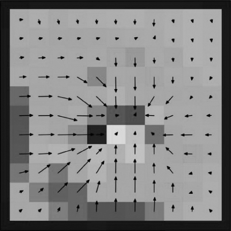
FIGURE 7.19 (See color insert) Arrowplot.
The limitation of this approach is of course that it does not give any information of the depth in the sensor at which the distortion in the field occurs. For that, a tilted beam has to be used, but such an approach requires more time and complex postprocessing. This method is faster and still gives an indication of the field and an accurate representation of how the image would be distorted in an x-ray imaging application.
Another common type of defect in CdTe hybrid pixel detectors is single pixel defects, where one pixel has low or no response while it is surrounded by pixels with a slightly higher than normal response. One such defect was scanned with the same kind of pencil beam as the blob defect but in this case the scan was done only in one row and in subpixel steps of 20 μm.
To investigate the charge transport, the cluster size at each position was studied. A cluster is defined as the pixels responding from a single photon interaction. To be able to resolve these the beam had to be strongly attenuated. The cluster size gives a good indication of the amount of diffusion during the charge transport. As shown in Figure 9.20a the cluster size increases at the edge of the pixels, which is expected since the charge cloud is then spread over two pixels, but it also increases when crossing the defect showing a maximum in the center of the defect pixel.
The total energy deposited in each cluster was also measured using the ToT mode of the Timepix chip. In Figure 7.20b, the total value for the cluster is presented as a function of its position. There seems to be no loss of charge when the beam passes the defect but rather the charge is spread over a larger area and collected in the neighboring pixels.
One possibility for this behavior is the high resistivity in the pixel contact or in the bump bond that connects the pixel. This would result in a lower electrical field and therefore more diffusion. The effect is also more visible with low-energy photons interacting high in the sensor, further strengthening this belief.

FIGURE 7.20 (See color insert) Line scan in 20 μm steps over a single pixel defect in the CdTe detector with 110 μm pixels. The vertical lines show pixel borders. (a) Cluster size; (b) cluster TOT.
The bright lines shown in Figure 7.18 are characteristic of pixellated CdTe detectors. A study by Hamann et al. [23] matched the lines to similar features in a back-reflection white-beam topography map. Further studies with the scanning rocking curve (SRC) showed that the borderlines correspond to mutually tilted regions in the crystal, revealing small-angle subgrain boundaries and/or dislocation networks.
In flood exposures (as Figure 7.18), the lines show a slightly higher count rate (10%) in electron collection mode and lower count rates in hole collection mode. The depth effect of the lines was investigated by scanning the lines with a tilted pencil beam and then reconstructing images from different depths in the sensor shown in Figure 7.21. The scan was also done with different threshold settings to extract information on the pulse height. For a threshold set at 6, 15, or 30 keV, the lines were between 1.1 and 1.3 times brighter than the rest of the matrix but with no significant depth dependence. Looking at the image of a 60 keV threshold there is a strong depth effect with the lines being as much as eight times brighter at the top of the sensor. Within the resolution of the Timepix chip, the lines remain in the same place throughout the depth of the sensor as expected if they are low-angle subgrain boundaries.

FIGURE 7.21 (See color insert) (a,b) Line defects at different depths in a 1 mm thick CdTe sensor for two different threshold settings: (a) 6 keV and (b) 60 keV.
The lines have been correlated with areas that have higher leakage current, but the use of a PC approach with leakage current compensation should not be affected by this. However, variations in leakage current will affect the electrical field in a high-resistivity material. Having the lines more visible even when the trapping should be increased along the subgrain boundaries further strengthens the theory that the effect of field distortion can be seen. This is also supported by the fact that the lines appear darker in hole collection mode since charge carriers of the opposite sign should be diffused instead of focused.
Using the detector in hole collection mode immediately reveals the poor transport properties of holes in CdTe. Looking at the flood exposures in Figure 7.22, the sensor shows a large number of defects and inhomogeneities. Also, a strange circular defect appears in some detectors. It is almost perfectly circular and either unresponsive or with noisy pixels inside. Operating the same chip in electron collection mode the defect is not visible at all.
The defect has been scanned with a pencil beam at 30° in order to characterize it. In hole collection mode the charge is clearly pushed away from the center of the defect (Figures 7.23 and 7.24). The effect depends strongly on the depth of interaction as holes created in the top layer are affected by the electrical field over a longer time than holes created near the pixel contact. Repeating the same scan in electron collection mode does not reveal anything and the sensor is working correctly in the whole scanned region.

FIGURE 7.22 Flood exposure in hole collection mode at different bias for a 1 mm thick CdTe sensor with a 55 μm pixel pitch bump bonded to Timepix.
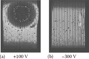
FIGURE 7.23 (See color insert) (a,b) Sum of all scan steps through the circular defect. Shown for both electron and hole collection mode.
The fact that the effect is present throughout the whole depth and is not visible at all in electron collection mode points to it being located at the surface and injecting charge when positively biased. The large current affects the electrical field and repels the charge created from radiation interaction. Given that the defect is only visible in one polarity, it probably behaves as a diode, blocking the current in one direction. To fully understand this defect, further investigations are needed.

FIGURE 7.24 (See color insert) (a,b) A single scan step showing the displacement of the signal.
7.5 OUTLOOK AND FUTURE CHALLENGES
To be a viable alternative for medical imaging, single PC detectors must be available with a high-Z sensor material to provide sufficient absorption up to 140 keV. Currently, the best candidates are CdTe and CdZnTe but even though these materials have greatly improved in recent years, much research is still needed to produce large volumes of high-quality material at a reasonable price. Reducing point defect and polarization will be a key development. Silicon can still be useful in some medical imaging application using lower energies, for example, the edge on silicon strip detectors has shown good results in mammography [24].
On the ASIC side, the big challenge is the high flux in CT measurements since pileup affects both the count-rate linearity and the spectral response. One way to counteract that is to use smaller pixels but this is also a balance since smaller pixels will lead to more charge sharing. In this respect, the Medipix3RX chip offers an interesting combination of small pixels and good energy resolution. Also important for medical applications and imaging applications in general is the size of the detector. Currently, the largest produced module in the Medipix family detectors is 14 × 14 cm2 [25] and even though larger modules are available with the Pilatus chip, these come at a steep price and with relatively large dead areas between sensors.
Efforts have been made to produce large-area detectors using edgeless sensors and through-silicon vias but the technology is still at an early stage. However, there is no doubt that the current movement in medical imaging is toward PC systems with spectral resolution.
1. X. Llopart, et al., Timepix, a 65k programmable pixel readout chip for arrival time, energy and/or photon counting measurements, Nucl Instrum Methods Phys Res A, 581(1–2), (2007), 485–494.
2. R. Ballabriga, et al., The Medipix3RX: A high resolution, zero dead-time pixel detector readout chip allowing spectroscopic imaging, J Instrum, 8, (2013), C02016.
3. W. Barber, et al., Characterization of a novel photon counting detector for clinical CT: Count rate, energy resolution, and noise performance, Proc SPIE, 7258, (2009), 725824.
4. P. Pangaud, et al., XPAD3: A new photon counting chip for X-ray CT-scanner, Nucl Instrum and Methods A, 571(1–2), (2007), 321–324.
5. R. Bellazzini, et al., Chromatic X-ray imaging with a fine pitch CdTe sensor coupled to a large area photon counting pixel ASIC, J Instrum, 8, (2013), C02028.
6. R. Dinapoli, et al., EIGER: Next generation single photon counting detector for X-ray applications, Nucl Instrum and Methods A, 650(1), (2011), 79–83.
7. P. Valerio, et al., A prototype hybrid pixel detector ASIC for the CLIC experiment, J Instrum, 9, (2014), C01012.
8. Medipix, The Medipix2 and Medipix3 collaboration, Medipix, http://www.cern.ch/medipix.
9. V. Pugatch, et al., Metal and hybrid TimePix detectors imaging beams of particles, Nucl Instrum and Methods A, 650(1), (2011), 194–197.
10. J. Jungmann, et al., Biological tissue imaging with a position and time sensitive pixelated detector, J Am Soc Mass Spectrom, 23, (2012), 1679–1688.
11. A. Kazuyoshi, Charged particle tracking with the Timepix ASIC, Nucl Instrum and Methods A, 661(1), (2012), 31–49.
12. P. Kraft, et al., Characterization and calibration of PILATUS detectors, IEEE Trans Nucl Sci, 56(3), (2009), 758–764.
13. J. Jakubek, Precise energy calibration of pixel detector working in time-over-threshold mode, Nucl Instrum and Methods A, 633(1), (2011), S262–S266.
14. J. Giersch, et al., The influence of energy weighting on x-ray imaging quality, Nucl Instrum and Methods A, 531, (2004), 68–74.
15. M. Sánchez del Río and R.J. Dejus, XOP: A multiplatform graphical user interface for synchrotron radiation spectral and optics calculations, Proc SPIE, 3152, (1997), 148–157.
16. J. Lawrence et al., HEXITEC ASIC—A pixellated readout chip for CZT detectors, Nucl Instrum and Methods A, 604(1–2) (2009), 34–37.
17. D. Greiffenberg, et al., Energy resolution and transport properties of CdTe-Timepix-Assemblies, J Instrum, 6 (2011), C01058.
18. T. Koenig, et al., Charge summing in spectroscopic x-ray detectors with high-Z sensors, IEEE Trans Nucl Sci, 60(6), (2013), 4713–4718.
19. ACRORAD, CdTe, http://www.acrorad.co.jp/.
20. Diamond Light Source, I15: Extreme conditions beamline at Diamond Light Source, Diamond Light Source, http://www.diamond.ac.uk/Home/Beamlines/I16.html.
21. L.-A. Hamel, et al., Charge transport and signal generation in CdTe pixel detectors, Nucl Instrum and Methods A, 380(1–2), (1996), 238–240.
22. F. Krummenacher, Pixel detectors with local intelligence: An IC designer point of view, Nucl Instrum and Methods A, 305(3), (1991), 527–532.
23. E. Hamann, et al., Applications of Medipix2 single photon detectors at the ANKA synchrotron facility, in 2010 IEEE Nuclear Science Symposium Conference Record (NSS/MIC), Knoxville, TN, 30 October–6 November, pp. 3860–3863, IEEE.
24. M. Lundqvist, Evaluation of a photon counting X-ray imaging system, IEEE Trans Nucl Sci, 48(4), (2002), 1530–1536.
25. WidePix, http://www.widepix.cz.