
The most important criterion in packaging consists of thermal management. It is not only the avoidance of the maximum temperature rating for device protection, but also the desire to operate at lower temperature. The power semiconductor devices operate better at lower temperature, with performance maintained within the specified data. Moreover, the lifetime of a power semiconductor device depends strongly on the temperature it operates at. A rule of thumb for silicon devices is that failure rates often double for every 10–15°C rise in operating temperature beyond 50°C [1].
After the power loss has been calculated at device level, the cooling system can be dimensioned. Thermal calculations are subsequently performed at all levels:
• At device level, for heat transfer from the semiconductor die to the external heat-sink and/or the selection of the device’s package;
• At converter level, for selection of the heat-sinks or cold-plates and the calculation of the radiated ad conducted heat toward the exterior;
• At equipment level, for selection of the enclosure.
All power semiconductors dissipate their switching and conduction losses and these should be removed as fast as possible. As this power is mainly removed through a contact surface with a cooling system, the whole size of the power converter and the power density within the equipment depend on the quality of the thermal transfer through the selected cooling system. Modern power converters expect a power removal of up to 200–500 W/cm2—that represents about half of the mean power density of the sun’s surface.
A model for a typical thermal circuit of a power semiconductor device is presented in Figure 7.1 and the change in temperature from the junction to the cooling agent (Tj − Ts) under a given power dissipation P is provided by the following relationship:
(7.1) |
where Rthjc represents the junction-to-case thermal resistance, Rthcs represents the case-to-cooling thermal resistance and Rthss represents the thermal resistance of the cooling system from the cooling agent (air, water, liquid) to the surface. It is, therefore, obvious that a lower equivalent resistance will keep the junction closer to the temperature of the cooling agent. The first two terms are provided by the semiconductor device datasheet and they are the same for a given device. The thermal resistance of the silicon itself is only 2–5% of the total thermal resistance, and the thermal properties of the cooling system are more important. Among these, the dependency of the thermal resistance on the thermal conductivity variation with temperature is very important for thermal modeling. Fortunately, this dependency for materials like Aluminum and Copper is minimal, and we can assume a quasi-constant thermal resistance for the entire operation range.
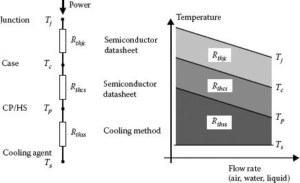
FIGURE 7.1 Equivalent model of a thermal system for a semiconductor device.
The second issue with Equation 7.01 relates to the interpretation of temperatures [2]. Thermal analysis in three-dimensional systems has pointed out the temperature variation on every geometrical direction, even on a state of equilibrium. The temperature values of Equation 7.01 are an average approximation of the reality, and the entire theory herein presented is neglecting the actual temperature distribution. Equation 7.1 can also be seen as an one-dimensional analysis.
The solution for improvement for a given structure is to go to higher ratings in order to minimize the thermal resistance. The last term in Equation 7.1 corresponds to the cooling system, and that depends on the method chosen, the cooling agent, the material and shape of the heat-sink or cold-plate, the flow rate of the cooling agent, and so on. Let us analyze the options we have.
Figure 7.1 shows that the higher the flow rate, the smaller the thermal resistance and the better the cooling. However, the cooling device itself and the connecting pipes, heat-sink, or cold-plate limit the flow rate of the cooling agent. Secondly, let us note the multitude of choices for cooling systems and their selection depends on the system requirements and cost (Figure 7.2).
The cooling agent can be air, water, or a special agent with a larger heat capacity. For example, removing the same power dissipation of 244 W from a three-phase converter produces an increase of 40°C on an air-cooled heat sink and only 2.8°C rise in a water-cooled system. Liquids with better heat capacity are based on different glycol solutions [3].
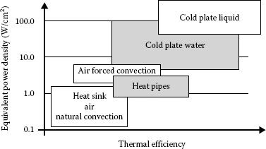
FIGURE 7.2 Thermal efficiency of different methods used for cooling.
The simpler solution consists of air cooling. A heat spreader is therein necessary to interface between the device/heat-sink and the ambient. This can be a simple copper or aluminum plate, or a more complex heat-sink structure. For example [5], the temperature drop across a 1 mm thick copper plate is approximately 0.25°C at a heat flux of 10 W/cm2, and it increases to 2.5°C at 100 W/cm2 or 12.5°C at 500 W/cm2. Heat spreaders are quite effective at low heat fluxes and may become unattractive at higher heat fluxes. This conclusion made room for liquid cooling (Figure 7.2).
Historically, the liquid cooling was not very attractive near electronic equipment. As the power electronics matured, the new development efforts moved from the power electronics converter to the auxiliary equipment, including the heat removal devices. First liquid-cooled systems were introduced in 1982 to large-scale integrated circuits [5]. The emergence of insulated gate bipolar transistor (IGBT) devices in early 1990s has also boasted the use of liquid cooled cold-plates in power electronic equipment. Today, the liquid cooling is the method of choice for medium and high power converters.
Most liquid cooling systems are water based and need to be protected from freezing (Figure 7.3) and this needs to target temperatures where the first ice crystals are formed and the flow is jeopardized. For this reason, ethylene glycol was used in solutions up to 40%. The recent focus on environment recommended the use of propylene glycol instead of ethylene glycol (Table 7.2). Either type of glycol needs to be pure enough in the sense it does not contain other additives like those used in automotive applications.
Once the method has been selected, the type of cold-plate or heat-sink is the next area of focus [5]. Different materials like aluminum or copper are used in manufacturing (Table 7.1) and their shapes can be different to facilitate the easy transfer of thermal energy. Materials and shapes of thermal devices able to handle these requirements are designed and selected based on knowledge of physical laws of thermal conduction, thermal radiation, and nature of forced convection or phase convection. The final criterion here is the cost of the device, as a more complex mechanical structure able to remove more heat will also cost more.
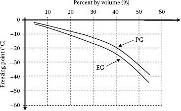
FIGURE 7.3 Freezing point of various cooling agents (EG = ethylene glycol, PG = propylene glycol).
7.1.2 TRANSIENT THERMAL IMPEDANCE
All the previous analyses have focused on steady-state thermal aspects when the average loss of power is known. In many applications, power semiconductor devices are stressed by transient over-currents with large instantaneous dissipation.
Modeling transient thermal impedance requires definition of a new parameter, heat capacity. This represents the rate of change of the heat energy with respect to the material temperature. The heat capacity per volume yields:
(7.2) |
The transient behavior of the junction temperature is related to the time-dependent heat diffusion equation with a simplified solution given by the analog equivalent circuit shown in Figure 7.4, and often called the Cauer model. The equivalent of the heat capacity is a capacitor able to slow down the junction temperature variation when a step change in power is applied. The ground potential represents the ambient temperature, and the heat capacities are connected from each node to the ambient (ground potential). This model can easily be implemented on any software for simulation of electrical circuits. As an alternate option, the Foster model is considering all thermal capacitors connected in parallel with equivalent thermal resistances. More recent computer models consider three-dimensional modeling of the heat transfer.
TABLE 7.1
Thermal Conductivity of Different Materials Used for Heat Extraction
Material |
Thermal Conductivity (Cal-g/cm2/s/°C) |
Water |
1.00 |
Steel |
0.11 |
Aluminum |
0.50 |
Copper |
0.92 |
TABLE 7.2
Liquid Thermal Conductivity
Fluid |
Thermal Conductivity (W/m K) |
Water (fresh) |
0.609 |
Ethylene glycol |
0.258 |
Propylene glycol |
0.147 |
Identical to the analog circuitry, a thermal time constant can be defined as
(7.3) |
Packaging materials and structures are always designed to minimize the thermal resistance as the loss power is transferred usually in average. For this reason, the thermal time constant and the power transient capability of a device are limited. However, it has been proven that power semiconductor devices can withstand large overload capabilities that exceed their average power ratings. Completing Figure 7.1 with the transient model yields the equivalent circuit shown in Figure 7.5. The temperature evolution in space when a pulse power is applied is also shown.
Transient thermal models are very useful in thermal analysis of power converters switched at high frequency with a variable duty cycle. The cooling system should sustain pulses of power with considerable thermal dynamics.
As an example, let us consider a three-phase power converter that supplies intermittently a motor fan. The steady-state operation of electronics has depicted 240 W of power loss. The fan works for 20 s at each 60 s. A very simple Cu plate used for cooling will allow a steady-state temperature increase of ΔTjav = 32 K. The simulation results for the complete thermal dynamics are shown in Figure 7.6.
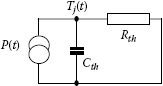
FIGURE 7.4 Transient thermal model.
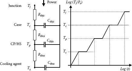
FIGURE 7.5 Transient equivalent circuit and temperature evolution in space.
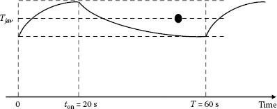
FIGURE 7.6 Transient thermal behavior of the considered example.
7.2 THEORY OF RELIABILITY AND LIFETIME—DEFINITIONS
From a mathematical perspective, reliability represents the probability that a product performs its intended function without failure under specified environment conditions, for certain time. Reliability can also be shown as a probability distribution of cumulative failures. The analytical expression yields as
(7.4) |
Over the years, the term reliability got a wider connotation, as it is mostly used beyond its analytical meaning, to express the quality of being reliable, that is the extent to which an experiment, test, or measuring procedure yields the same results on repeated trials.
The failure rate can be expressed as f(t):
(7.5) |
For a constant failure rate:
(7.6) |
This definition is not very friendly as it deals with very small numbers. As an alternative, we may use the failure rate in a specified time interval of 1 × 10⁹. This allows us to define FIT (failures-in-time) as
(7.7) |
In equipment where high reliability is a must, failure rate of the semiconductor devices usually range from 10 to 100 FIT (1 FIT = 10–9/h) [44].
Mean time between failures (MTBF) is the predicted time between inherent failures of a system during operation. This means:
(7.8) |
Lifetime of an electronic component is specified as the time at which the electrical parameters have drifted out of some specified limits mainly due to wearout (Figure 7.7). In reality, during the time interval with a constant failure rate, failures due to improper use of devices or due to accidental ambient factors may happen and they are generally identified as random failures. As a rule of thumb, if the failure rate during the usage interval (interval with random failures) is above 0.1%, one should revise carefully the design of that system.
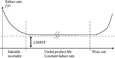
FIGURE 7.7 Bathtub curve for lifetime of a power electronics equipment.
All of these measures for reliability have a statistical character. Data can be depicted from numerous experimental or field test data or determined by accelerated power and temperature cycling tests.
Reliability of power electronics equipment has become a priority for any system developer [6]. Once the knowledge about the power electronics equipment perfected, the studies of reliability became a priority. As of 2012, reliability is one of the most dynamic fields of interest in power electronics. While studies are dedicated to different application fields (integrated circuits [7], energy distribution networks [8], wind energy [9,10], distributed generation [11], photo-voltaic systems [12], high-power converters [13]), this Chapter provides a general introduction to reliability of power electronic equipment.
In order to improve device lifetime and reliability, efforts are made at all phases of device’s life:
• During the manufacturing process, attention is paid to quality. Statistical process control (SPC) is the application of statistical methods to the monitoring and control of a process to ensure that it operates at its full potential to produce conforming product. This is necessary in order to produce as much conforming or reliable devices and systems with the least possible waste.
• During operation, the ambient conditions are severely monitored and the control system adapts depending on the external factors. Advanced control systems are designed to withstand a variety of environmental conditions or variation of parameters, generally considered as uncertain parameters or disturbances. In this respect, modern computer-based simulation and optimization tools allow design under complex criteria. Probably the most important example of a robust control technique [14] is H-infinity loop-shaping, which was developed by Duncan McFarlane and Keith Glover of Cambridge University. The H-infinity loop-shaping method minimizes the sensitivity of a system over its frequency spectrum, and this guarantees that the system will not greatly deviate from expected trajectories when disturbances enter the system. Another example is LQG/LTR, which was developed to overcome the robustness problems of LQG control.
• Given the complexity of operation and failure constraints, modern control systems are joined by expert systems. Design for reliability (DFR) includes an advanced fault management system able to decide on the operation of the power electronic equipment when special situations or random faults occur. Expert systems are able to predict failure, to provide scenarios for getting out of failure mode, and/or operation optimization for minimization of risks. Fault management system is a simple example of an expert system targeting reliability improvement. A particular case is the design with redundancy. This means that if one part of the system fails, there is an alternate success path, such as a backup system. An UPS system might use two batteries. If one battery fails or gets discharged, the UPS still operates using the other battery. Redundancy significantly increases system reliability, and is often the only viable means of doing so.
• Accurate lifetime prediction should help scheduling the replacement of each individual component and the periodic maintenance. This is usually achieved with accelerated test plans. Because reliability is a probability, even highly reliable systems have some chance of failure. A single test is not able to generate enough statistical data. Multiple tests or long-duration tests are usually very expensive. In order to secure the statistical information necessary for failure and reliability analysis, a set of experiments is specifically designed with the method of design of experiments, which has been developed by people like G. Taguchi. The method consists of introducing noise factors into experiments in order to quantify different effects and to use a signal-to-noise metric. The design of experiments method is heavily used in manufacturing for calibration of the robust design process. Different sets of tests are required for assessing the lifetime of various power devices and systems. The purpose of accelerated life testing is to induce field failure in the laboratory at a much faster rate by providing a harsher, but representative environment. In such a test, the device or system is expected to fail in the laboratory just as it would have failed in the field (but in much less time), based on destructive energy equivalence. This helps to discover failure modes or to predict the normal field life from the high-stress life. Establishing the appropriate accelerated test plan is a science by itself.
The failure rate of the entire system is calculated from the failure rates for each individual component. In most systems, like it is the case of power electronics circuits, all components are considered as being important. From reliability point of view, this means that the components are considered as being “in series” within the system. In a series system that includes n components, the overall failure rate λSYSTEM is given by
(7.9) |
where λi corresponds to the individual failure rates of the elements [15].
Even for components manufactured under identical conditions, the failure rates in the field can vary by a factor of 10 depending simply on the conditions the device was used [44]. Each individual component is considered to have a constant failure rate (λ), which is weighed (derated) through a series of stress factors.
(7.10) |
The stress factors (πi) refer to temperature, voltage stress, circuit/application, rating, environment, construction factor, and product quality, respectively. They have the meaning of derating the datasheet information for the constant failure rate depending on manufacturing, environmental conditions, and circuit use of devices.
As an example, let us consider a silicon rectifier diode [44] with a maximum rated current of 1 A, at an ambient temperature of 30°C, and a rated maximum junction temperature of Tjmax = 150°C. The rectifier has an actual operation at a current of 0.5 A, at 40% of the rated voltage, at ambient temperature, on a system fixed to the ground, with a junction temperature of Tj = 100°C. The datasheet also provides the base failure rate of λbase = 0.0010/106 h. The manufacturer is also providing the following weigh factors:
πE = 6.0 for a fixed application (on the ground)
πQ = 2.4 and πC = 1.0 for the specific production line
πT = 8.0 when operated at Tj = 100°C
πS = 0.11 at 40% of the rated voltage
Using the above values, λP is calculated as follows:
(7.11) |
In most cases, the steady-state temperature is the only factor incorporated in the model (πT). For instance, an IGBT device operated always at a junction temperature of 125°C will have a shorter lifetime than the same device operated always at a junction temperature of 75°C. This dependency is illustrated by the Aarhenius law:
(7.12) |
where Edev represents the thermal activation energy of a particular failure, and K is the Boltzman constant = 8.617 × 10⁻⁵ eV/K. This can be shown in a similar form as
(7.13) |
The thermal activation energy (or simply called activation energy) concept comes from chemistry where it represents the minimum amount of energy required to convert a normal stable molecule into a reactive molecule. The activation energy levels for different failure modes of power semiconductors are in the range 0.1… 2.0 [eV].
Since different wear-out mechanisms are possible (see later on, Section 7.3.4.), each one can be provided a failure rate characterized with a different activation energy and the equivalent activation energy value for the entire system is calculated based on the dominant failure [16] or based on a weighed activation energy. Since the energy activation and the weigh factors depend mainly on the manufacturing of power semiconductor device, it is very difficult to maintain a single set of weighs. This is why the use of the activation energy method for reliability calculation has its pros and cons.
It is possible to neglect the variation due to factors other than the steady-state temperature since this is the most important stress factor. Analogous to the Aarhenius equation, other relationships are available to characterize other stress factors. Furthermore, other common ways to determine the life stress relationship are: the Eyring Model, the Inverse Power Law Model, the Temperature-Humidity Model, the Temperature Nonthermal Model.
7.3.3 FAILURE RATE FOR DIVERSE COMPONENTS USED IN POWER ELECTRONICS
The base failure rate, reliability, or MTBF for each individual component is provided by manufacturer or by industry standards. The industry standards are more generic, and do not take into account the specifics of each production line. The manufacturer provided reliability data is based on measurements and accelerated life tests. They provide base values for each product that still needs to be weighed with the actual operation conditions (environment and circuit).
Table 7.3 shows example of data depicted from the U.S. military standard MIL-HDBK-217. As will be shown later on, this type of standards regulation does not provide data about high power switching semiconductor devices, and data needs to be adapted from conventional transistors or modules.
All of these components are present in different power electronic structures. In medium and high power converters, the power semiconductors are more important. As shown before, the failure of the entire system is given by the failure rates for each component. Hence, the most critical component is the DC link electrolytic capacitor.
TABLE 7.3
Example of Failure Rates for Electronic Components
Description |
Type |
MTBF (Years) |
Connector |
Per pin |
2283 |
Semiconductors |
Si diode |
2283 |
Si transistor |
1426 |
|
Resistor |
Carbon |
11,415 |
Wire-wound |
4566 |
|
Film |
2283 |
|
Capacitor |
Electrolytic |
76 |
Tantalum |
114 |
|
Paper |
228 |
|
Ceramic |
456 |
|
Plastic film |
5707 |
|
Magnetics |
Power inductor/copper |
2283 |
Transformer/copper |
570 |
Capacitor lifetime is limited by electrochemical degradation that proceeds in predictable manner, accelerated by environmental factors like temperature and voltage stress. Historically, the lifetime of electrolytic capacitors has progressed from 1000 h at 65°C, 40 years ago, to 15,000 h at 105°C today [17]. The predicted lifetime at a given temperature yields with the Arrhenius law equations used by all commercial capacitor vendors. For instance, a capacitor rated with 10,000 at 105°C, could survive 160,000 at 65°C.
The reliability of the power semiconductor module depends on many different physical and chemical processes. It can be demonstrated that power semiconductor module could contribute better performance for the system reliability than individual components [18]. Moreover, a power module provides a better thermal design and an excellent layout, both with effects on the system reliability. Using a power module supplied from the manufacturer rather than using individual components is recommended for the inverter application.
7.3.4 FAILURE MODES FOR a POWER SEMICONDUCTOR DEVICE
As the most part of the R&D is dedicated to reliability calculation and improvement for the power semiconductor devices, they will be presented in more detail in what follows.
There are two major categories of failure in power electronic equipment:
• Random (accidental) failures
• Wear-out mechanisms
Manufacturers of power semiconductor devices consider reliability within the new technologies [19]. The safe-operating-area needs to be enlarged so that devices are extremely rugged, capable of withstanding current, voltage and temperature conditions well in excess of their nominal continuous ratings.
7.3.5 WEAR-OUT MECHANISMS IN POWER SEMICONDUCTORS
The most observed failures due to wear-out mechanisms for a power semiconductor device are package related and they are accelerated by thermo-mechanical stress [20].
Considering operation of power electronics equipment for a long enough time interval will show changes in parameters. These changes can be globally called wear-out mechanisms. They occur both in the semiconductor die and the mechanical packaging [21].
Examples of wear-out mechanisms in the packaging and assembly of power semiconductors:
• Bond wire
• Bond wire lift-off
• Bond wire heel crack
• Damage of the AL metallization
• Electromigration in the bonding wires
• Solder joints degradation
• Aging of the direct copper bond
• Cracks and void formation
• Delamination of copper metallization
• Die fracture due to other pre-existing defects
Examples of wear-out mechanisms in semiconductor die (mostly similar to those studied in microelectronics) [22,23]:
• Ionic contamination
• Hot carrier injection
• Slow trapping
• Gate–oxide breakdown
• Negative bias temperature inversion
The thermo-mechanical wear-out processes are the most important [24]. Any of these wear-out mechanisms can be analyzed individually with the thermal activation energy concept.
The ageing of devices (wearout) is accelerated by operation under application-related stress factors like the repetitive protected short-circuit [25]. A critical energy has been defined in [25] to account for the cumulative degradation effect of repetitive short-circuits while enough time was allowed between short-circuits for device cooling. It has demonstrated that it takes around 10,000 protected short-circuits to reach failure of a conventional 600 V IGBT [25].
The repetitive short-circuit events produce a thermal cycling with a large temperature difference within the IGBT. This thermal cycling introduces repetitive compressive and tensile stress in the emitter metallization film due to the CTE mismatch between aluminum metallization and the silicon chip. This stress leads to high plastic deformation with effects in increasing of the metallization resistance and weakening of the bond wire contacts (resistance produces more dissipation, hence increase in local temperature, and fatigue follows).
After understanding all the possible wear-out mechanisms and what it takes for them to occur, the design engineers are setting condition monitoring systems able to tell at each moment the actual status of the component or subsystem and how many hours are still available before the next maintenance checkup. Such systems are well known from laptop computers, where the battery status is monitored based on the amount of hours it is used, and the predicted lifetime is at any time reported to the user. Similar systems are to be implemented for IGBT-based equipment and their studies are in a very embryonic state [26]. The idea is to monitor and measure in-circuit the most important device parameters (gate threshold voltage, leakage current, voltage drop in conduction) along with the operating temperature and to assess the performance degradation and ageing of the IGBT device from such information.
7.4 LIFETIME CALCULATION AND MODELING
Lifetime calculation for given equipment comes down to applying the analytical formula onto the lifetime rates for each individual component. The modeling and/or calculation of lifetime rate for each component is done usually independent of the final equipment. The lifetime of each component is investigated by analyzing all the possible failures. A fault tree is built sometimes based on experimental (field) evidence [27]. Each individual failure mechanism is isolated and further investigated by appropriate testing or by physical modeling (Figure 7.8).
If the failure rate for an individual failure mode needs to be determined by experiment, a set of accelerated tests is adopted since most failure mechanisms are based on accumulated degradation (wearout) that occurs after long time in practice.
The second possible approach for determination of the failure rate for a certain failure mode is based on physical description of the system. Equations for operation under specified circuit and environmental conditions are required to qualify the production of failure. At this moment, the method of physics of failure is more developed for semiconductor materials (microelectronics) and under major investigation for thermo-mechanical failures (packaging).
Let us assume some equipment has failed at a given moment after hours of proper operation. The obvious question is “what happened?” and the first reaction would be to blame an external event. If no obvious external event has occurred (there was no mechanical, thermal or electrical stress unexpectedly coming from outside the proper operation of each device/component within the equipment), the investigation should go back toward the manufacturing methods and the technology inside each device. Each device or component within that equipment is subjected to multiple failure mechanisms, each mechanism being triggered by its own accumulated degradation. The multiple mechanism model extrapolates independent acceleration factors for each component’s mechanism of concern based on the component’s stress states. The concept of acceleration factor and the thermal dependency of each accumulated degradation mechanism will be studied in the next section (Figure 7.9).
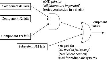
FIGURE 7.8 Example of fault tree for a power converter.
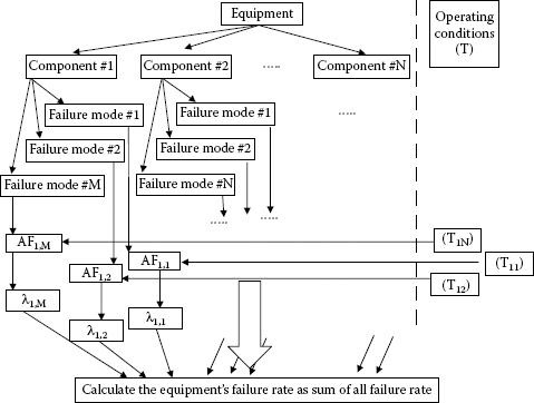
FIGURE 7.9 Multiple mechanism model.
7.4.2 ACCELERATED TESTS FOR ELECTRONIC EQUIPMENT
7.4.2.1 Using the Activation Energy Method
Since the expected lifetime of power electronics equipment is between 10 and 30 years, it is not practical to gather data from actual life experiments. Some technologies or newer generation of devices were not even imagined 30 years ago. For this reason, the lifetime is estimated by accelerating the stress factors. The qualification tests last for a shorter time, and the statistical model of lifetime prediction can be determined more easily.
Given the multiple stress factors from Equation 7.09, it is practical to limit the qualification tests to temperature as the main stress factor. Accelerated tests are therefore designed for temperature as the unique stress factor. Reconsidering the Aarhenius law:
(7.14) |
Helps depicting the time to the failure as
(7.15) |
Therefore, the actual time-to-failure/temperature dependency belongs to the same characteristics with the accelerated-time-to-failure/test-temperature point. By selecting a test stress temperature Ts, and measuring the test-time-to-failure τs, one can get information about the actual time-to-failure τ0 when operated at a lower actual temperature T0 (Figure 7.10). Such tests are also referred to as HAST (highly accelerated stress tests).
It is common to define an acceleration factor:
(7.16) |
Let us consider an example. Several samples for a power converter product have been tested at 125°C and the statistical time-to-failure was determined as 1000 h for a known failure mode with the activation energy of 0.5 eV. Measurements for the consistent operation of the converter in the field show operation at a temperature of a 50°C. The acceleration factor yields:
(7.17) |
Hence, the prediction for the time-to-failure within the actual operation conditions yields:
(7.18) |
If there are multiple known failure modes of the same device, a generic (weighed or averaged) thermal activation energy can be considered. Alternatively, a more accurate modeling would consider all the possible failure mechanisms, each one with its own thermal activation energy and its own accelerated test plan. The lifetime has to be calculated from results pertaining to all failure modes (Figure 7.9). The failure rate in FITs (number fails in 109 device hours) yields:
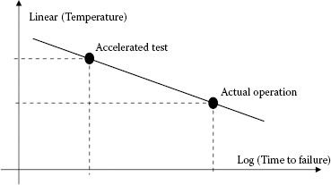
FIGURE 7.10 Accelerated tests for thermal related wear-out.
(7.19) |
where:
• β represents the number of distinct failure mechanisms considered for the study.
• k represents the number of different lifetime tests combined in the calculation of each failure (i).
• xi represents the total number of failures for a specific failure mechanism (one of β).
• TDHj represents the number of test hours before a certain failure (i).
• AFij represents the acceleration factor for the failure (i) associated with the test (j).
• M represents a factor determined by the confidence level for the estimation (so-called Chi square confidence value).
This method works both ways:
• When we want to predict failure rate for each component, independent of the operation, just for simulated accelerated tests, the direction is from accelerated tests to the nominal value (benchmark value).
• Otherwise, we may know a value for the nominal lifetime, and use the actual operating conditions to predict the actual lifetime considering within the acceleration factors the effect of the operating conditions.
The accelerated test plans can be designed for voltage stress or humidity stress. When both the temperature and voltage stress factors are used, the acceleration factor of the test should be calculated as a product A = AFT * AFV, where AFT is the thermal acceleration factor, and AFV is the voltage related acceleration factor. This is provided by the exponential law:
(7.20) |
However, the voltage and/or humidity derate are not very much used in practice for power electronics equipment.
Another accelerated test procedure refers to temperature cycling. This time, the effect of temperature change on the equipment’s lifetime is calculated. Each time the equipment powers up from ambient temperature to the actual operation, there is a gradient of temperature than influences the time-to-failure. This test is very important for the validation of the packaging and overall assembly and it does not require electrical power in the circuit. The device is heated and cooled by an external heat source, like an oven, to produce the variation in ΔTjc. Materials have different thermal expansion coefficients and the temperature cycling induces certain failures due to the thermo-mechanical expansion. Such failures can be package cracking, die cracking, wire-bond lift-off, and an increase in contact resistance.
The Coffin-Manson model is generally used to designing this acceleration test. The time-to-failure τ is proportional to [ΔT]n.
(7.21) |
where A is a constant. The acceleration factor yields:
(7.22) |
where ΔTs is the stress temperature difference and ΔTo is the actual operation temperature difference.
Let us consider an example. A temperature cycling test was designed with a temperature change from −65°C to 125°C. The statistically determined time-to-failure was 1000 cycles (the components failed after around 1000 cycles). The manufacturer of the component provides information about the modeling of the package with n = 6. What is the time-to-failure for the same system performing 100 cycles per day, with an actual temperature cycle between the ambient temperature of 25°C and the steady-state operation at 90°C?
First, we will determine the acceleration factor:
(7.23) |
The expected time-to-failure under actual operation conditions yields:
(7.24) |
7.4.2.3 Accelerated Tests for Power Cycling
Numerous motor drive applications require an operation with frequent acceleration and stops. This is the case of traction power converters for urban trains, elevators and so on. A short-distance train travels for only a few minutes between stops and is expected to operate 30 years in the field. This corresponds to a lifetime of 100,000–135,000 h and 5–10 million travel-stop cycles [32]. Other applications subjected to similar operation include different machine-tools, or home appliance equipment [31]. This operation with large gradients of temperature derived from frequently heating and cooling the power semiconductor devices favors specific wear-out mechanisms. Given the large spectrum of possible load profiles (like different distances between stops, and so on), it is virtually impossible to define a unique test profile. Field reports show that the use of IGBT devices in this operation mode with frequent stops, eventually led to wearout and failure related to
• Disconnection of the aluminum bonding wires from the silicon chips (bond-wire lift-off).
• Increase in module Rthjc.
In order to qualify the power electronics equipment for this type of operation, accelerated tests for power cycling have been designed [32]. These tests involve operation of the device with electrical power (Figure 7.11). The power semiconductor device is set-up for conduction under a permanent gate control. The collector current is externally switched on and off, and a very large value of the current is adopted. The junction temperature is closely monitored with the goal to emulate a very large temperature difference. The greater the variation in ΔTj – c, the greater the thermal stress, and the shorter is the power semiconductor lifetime. The same reasoning as explained in Figure 7.10 is adopted for the design of experiment (Figure 7.12).
Obviously, there are different variations of the test as different parameters and measurement methods differ [32,33,34,35].
A very different approach for the power cycling tests is specified in Section 8.2.6 of the IEC standard 60747-9 of 2001. It is named the “Intermittent operating life test” and is a power cycling test based on controlling the gate of an IGBT to turn on and off for cycling a very large load current. Most of the power cycling tests proposed by industry and academia in the past meets the requirements of the IEC test. However, they do not achieve power cycling by gate control. Hence, the difference between the two methods is that the IEC approach includes switching loss in the device while the switching loss is not present in tests where the device is held permanently on. This is not expected to significantly affect the test results.
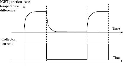
FIGURE 7.11 Principle power cycling.
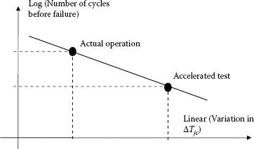
FIGURE 7.12 Accelerated tests with power cycling.
Once the test procedure has been decided on, the engineer needs to define the failure criteria. Usually, this is defined as one or multiple of the following:
• Increase of the conduction voltage drop by 5–20%
• Increase of the thermal resistance Rthjc by 20%
• Increase of the Gate-Emitter threshold voltage by 20%
• Increase of the leakage current by 20%
• Increase of the steady-state gate current by 20%
7.4.3 MODELING WITH PHYSICS OF FAILURE
There is a tremendous recent effort for the development of accurate failure models based on the actual physical operation of the device. The following steps are generally used in this respect:
• Identify the potential failure mechanisms.
• Expose the power semiconductor device to highly accelerated stress to find the dominant root-cause.
• Identify the dominant failure as the weakest link.
• Model the dominant mechanism.
• Combine the data.
• Develop an analytical model for the dominant failure.
7.5 STANDARDS AND SOFTWARE TOOLS
There are different standards that provide guidance for calculation of the reliability performance of electronic components. The most quoted reference is the U.S. Military Handbook for “Reliability Prediction of Electronic Equipment” (MIL-HDBK-217) [36]. The prediction based on MIL-HDBK-217 considers systems as being in a series that means any device failure is as important. A similar effort is assembled in the 3rd issue of Telcordia SR-332 (entitled “Reliability Prediction Procedure for Electronic Equipment”) released in January 2011 [37]. The Telcordia model for reliability of electronics equipment uses a black-box technique. The failure rate is calculated from a steady state failure rate, weighed by quality, stress and temperature ratios:
(7.25) |
Other standards are released by NERC and NIST for the U.S. power systems. Finally, International Electrotechnical Commission has elaborated two standards on the field [8]:
• The IEC 61709 standard was published in 1996, it is derived from a manufacturer standard and it is very similar to MIL standard. The failure rates and the influence factors are extrapolated from field data of items operating in different environmental conditions. They are referred to the equipment manufactured in the first half of 1990s.
• The IEC62380 standard was released in 2004, and compiles data collected in between 1999 and 2001 from the telecommunication sector. However, the standard is applicable to both ground and airborne equipment.
All of these standards provide models for conventional base components like resistors, capacitors, inductors, transformers, transistors and diodes. They do not include models for newer power devices like IGBTs, GTO, IGCT, and the like. There is actually no standard available for models pertaining to these power devices.
The European Power Supply Manufacturers Association has released in 2005 a document entitled “Guidelines to Understanding Reliability Prediction” [38]. The report presents results for an interview of 16 EU companies on the methods they use for reliability prediction. The results are very disappointing. For example the MTTF at room temperature (25°C) of a small 1 W DC-DC converter with 10 components ranged from 95 years to 11,895 years—a variation of 125:1! When it was agreed that the major reason for such variation was an inappropriate assumption to consider the potted product a “hybrid assembly,” re-calculation showed the variation to range from 1205 years to 11,895 years—a variation of 9.9:1.
We should expect in the near future, more effort on defining standards and procedures for reliability prediction. In this respect, let us note that on December 31, 2012, the North American Electric Reliability Corporation (“NERC”) filed with the Federal Energy Regulatory Commission a new reliability standard (EOP-004-2) that impacts the reliability of the power grid.
7.5.2.1 Tools Derived from Theory of Reliability
Information from these standards is used to elaborate software tools for reliability prediction and several examples of software tools are herein briefly revised. These solutions consider the electronic equipment in a kind of static operation, under a constant failure rate, without modeling the change of parameters in time (wearout). They simply convey the standards’ requirements into a software format. Since these solutions are provided by small companies, they may appear and disappear inadvertently, so this list is provided for understanding the current capabilities rather than an ultimate solution.
• DfR Solutions—Offers a software tool called SHERLOCK for reliability prediction within electronic PCB (printed-circuit-boards). The software is able to import bill of materials from a SPICE simulation, to build the FEA, and to define the product lifecycle in respect to vibration, shock, and temperature variation. It also has a section able to perform certain physics of failure analysis for solder joint fatigue, plated through-hole fatigue, ceramic capacitor breakdown, and IC wearout. During the years 2007–2011, a library of over 250 root-cause investigations were reported.
• T-Cube Systems—Offers RELCALC that is a direct implementation of MIL-217 standard. Similar tools are offered for more than 25 years.
• Relex Scandinavia—Offers a similar package called Relex Reliability Studio, since 1986.
7.5.2.2 Tools Derived from Microelectronics
On a different line of thought, wear-out models can be developed [39] for microelectronic devices within programs like:
• FaRBS [40] (the name comes from Failure Rate Based Spice) = It is able to estimate failure rates within microelectronic devices based on physics of failure and the method of sum of failures.
• BSIMProPlus of Cadence [41].
• RelXpert (formerly BTABERT) by Celestry provides a SPICE simulation of both the HCI and NBTI degradation for IC technologies below 0.13 μm.
These programs allow the modeling of the change with time of parameters like threshold voltage, transconductance, gate charge, leakage current, I-V characteristics (including the voltage drop on device). It is worthwhile to also mention the AgeMOS model [42] developed by Cadence, that includes device degradation due to hot carrier injection and negative bias temperature instability.
In 2003, IBM Corporation has elaborated a program called RAMP, able to model the wearout of semiconductor devices like microprocessor (microelectronics). It did use a competing risk model, incorporating failures like electromigration, stress migration, time-dependent breakdown, temperature cycling, hot carrier injection, and negative bias temperature inversion.
7.5.2.3 Power Electronics Specifics
Even from mid-1990s, efforts for computer-based estimation of reliability for power electronics equipment were reported [43]. Since there was not a program able to do both circuit simulation and reliability calculation based on the component’s constant failure rate weighed by the actual operation point, researchers have tried to pass data in between programs in order to achieve this goal [27,39].
As of 2012, a complete program for the prediction of reliability in power electronics is still not available. The knowledge from microelectronics and packaging technologies are complementary and we should expect a solution able to model both types of failures under the same model.
Due to the importance of thermo-mechanical failures caused by the mismatch in the Thermal Expansion Coefficient of the different joined materials within an IGBT, such failures are usually considered as major and followed alone for the estimation of lifetime. They usually lead toward bondwire liftoff or solder layer degradation.
Semiconductor failures like electromigration, time-dependent breakdown, hot carrier injection, negative bias temperature inversion, or even the gate oxide breakdown or passivation are well known in the microelectronics and their activation energy seems to be low enough to prevail also in power semiconductor devices. Their occurrence would change the IGBT’s parameters and accelerate the thermo-mechanical issues. This is probably why the power semiconductor companies direct their reliability efforts into two directions:
• Hot-carrier injection and the sistership phenomena of radiation hardening
• Minimization of technological parameter variation for sustaining a more robust design
Most of the so-called “Hi-Rel” power semiconductor devices are sold in the same packages as conventional IGBTs or MOSFETs. At most, the hermetic packages are considered to alleviate the occasional exposure to special environmental conditions like dust, or humidity.
In conclusion, the simultaneous occurrence of wearout in both microelectronics and packaging should be ideally considered within an advanced model. Applying the competing risk model helps us to reduce the analysis to microelectronics (semiconductor) failures for low power devices (like power supplies MOSFETs), and to thermo-mechanical packaging failures in high power devices like IGBT and IGCT.
Finally, let us note that any of these tools is not complete as nobody did merge them with conventional circuit simulators. This is one step the future should offer. For instance, there is no tool able to compute in a single step the answer to a question like “if in this converter I change the gate resistor from 10 Ohm to 20 Ohm, the MTBF goes from 100,000 h to 145,000 h.”
7.6 FACTORY RELIABILITY TESTING OF SEMICONDUCTORS
All power semiconductor manufacturers pass devices through a series of reliability tests according to their own methodologies [2,44]. Such tests can subscribe to two major classes:
• Initial burn-in tests to minimize the infantile mortality [45]
• Qualification tests based on samples
Even if methods differ from manufacturer to manufacturer, the qualification tests aim at meeting requirements from standards for discrete semiconductor devices like JIS C 7021 (Japan) or IEC60747, IEC60068, and IEC60749 (Europe). Such tests are intended to “pass” or “fail” the products based on certain failure criteria. These tests are accelerated test procedures established for the power device only, and are different from tests shown in Section 7.4.2 that are intended to simulate the actual use of the electronic equipment. They are based on production samples.
These qualification tests can be classified in three groups:
• Chip related tests (high temperature reverse bias test, high temperature gate stress, and so on)
• Stability of the package under specified operation and storage temperature (steady-state and transient)
• Mechanical integrity of the package (vibration and shock)
DFR represents an emerging discipline that refers to the process of designing reliability into products. During system design, the top-level reliability requirements are then allocated to subsystems by design and reliability engineers working together. As shown before, the reliability models use block diagrams and fault trees to provide a graphical means of evaluating the relationship between different parts of the system. These models incorporate predictions based on parts-count failure rates taken from historical data. While the predictions are often not accurate in an absolute sense, they are valuable to assess relative differences in design alternatives.
As an alternative, the physics of failure represents a design technique that relies on understanding the physical processes of stress, strength, and failure at a very detailed component level. This helps the redesign of each component to reduce the probability of failure. Most typically such evaluation of the physics of failure comes down to the test and introduction of new materials. The issues related to the reliability of the highly-integrated power modules as well as of various passive components represent a very active and promising field of research, requiring a multiphysics approach to thermal-mechanical strain control for controlled reliability and full capacity utilization.
The movement of the design effort from circuit design and validation toward proving sustainability and reliability of the design has opened up new R&D directions:
• Analysis of the suitability of a device or system for a purpose, with respect to time
• Determination of the capacity of a device or system to perform as designed, within conventional context or while taking advantage of new materials or knowledge
• Calculation of the resistance to operation under extreme conditions or in failure mode of a device or system, as well as the ability of a device or system to fail without catastrophic consequences
• Calculation of the probability that a functional unit will perform its required function for a specified interval under stated conditions
Pure reliability engineering relies heavily on mathematical models such as reliability prediction, Weibull analysis, thermal management, reliability testing, and accelerated life testing. Because of the large number of reliability techniques, their expense, and the varying degrees of reliability required for different situations, a more systematic and/or academic approach is recently considered.
The issues related to the reliability of the highly-integrated power modules as well as of various passive components represent a very active and promising field of research, requiring a multiphysics approach to thermal-mechanical strain control for controlled reliability and full capacity utilization.
A structural introspection outlines possible topics of research around a power module:
• Influence of semiconductor fabrication defects and defect migration under operation
• Heat-fatigue phenomenon in semiconductor modules, under thermal cycle and power cycle
• Stress at the bond wire–bond pad interface within a power semiconductor device is able to recommend the proper shape of the connection and to model the fatigue
• Stress at insulation substrate-base plate
With the increasing interest in reliability, there are numerous recent reports of cases when the reliability concerns were considered in the design phase. For instance, [46] reports a method for the on-line manipulation of the switching frequency and current limit to regulate the losses in order to prevent over-temperature and hence the power cycling failures in IGBT power modules.
This chapter makes an introduction to the thermal and reliability aspects related to the design of medium or high-power power electronics equipment. Thermal calculation is well known and was previously used to properly size the cooling systems.
The recent years has shown an increasing interest in reliability prediction. The theory of reliability is herein revisited and the peculiar aspects of applying this theory to power electronics equipment are revealed. Faults can occur through degradation of performance in both semiconductor die and thermo-mechanical setup. The most important failure mechanisms need to be qualified with experimental tests or by investigation of the physics of failure and analytical modeling. The experimental tests need to be designed based on theories of design of experiments, for either temperature cycling or power cycling. The analytical modeling needs a greater understanding of the physics of phenomena occurring during failure. In either case, monitoring of the actual operation characteristics helps accurate estimation of the lifetime. This helps anticipating failures and proper service or maintenance scheduling.
Finally, principles of DFR help us to consider reliability into early phases of design, in order to increase the product robustness and lifetime.
The entire field of reliability prognosis and estimation is under major investigation and we may expect to see more standards and software tools in the near future.
1. Sparrow, E.M., Chevalier, P.W., and Abraham, J.P. 2006. The design of cold plates for the thermal management of electronic equipment. Heat Transfer Eng. 27(7), 6–16.
2. Lutz, J., Sclangenotto, H., Scheuermann, U., and De Doncker, R. 2011. Semiconductor Power Devices—Physics, Characteristics, Reliability. Springer, Heidelberg/Dordrecht/London/New York.
3. Anon. 2002. Thermal management products. Application Note, Ferraz-Shawmut.
4. Sueker, K.H. 2005. Power Electronics Design—A Practitioner’s Guide, Ed. Newness/Elsevier, Amsterdam/Boston/Heidelberg/London/New York/Oxford/Paris/San Diego/San Francisco/Singapore/Sydney/Tokyo.
5. Kandlikar, S.G. and Hayner, II, C.N. 2009. Liquid cooled cold plates for industrial high-power electronic devices—Thermal design and manufacturing considerations. Heat Transfer Eng. 30(12), 918–930.
6. Blaabjerg, F. 2012. Power electronics and reliability in renewable energy systems. IEEE IECON Keynote Speaker.
7. Wyrwas, E.J. and Bernstein, JB. 2011. Quantitatively analyzing the performance of integrated circuits and their reliability. IEEE Instrumentation and measurement Magazine, February 2011, pp. 11–31.
8. Anon. 2007. Advanced power converters for universal and flexible power management in future electricity networks, Report D6.1, Project co-funded by the European Community under the Sixth Framework Programme.
9. Tavner, P. 2010. Reliability and availability of wind turbine electrical & electronic components. Durham University Document.
10. OKeefe, M. 2009. Thermal stress and reliability for advanced power electronics and electric machines. NREL Presentation at 2009 U.S.DOE Hydrogen Program and Vehicle Technologies Program Annual Merit Review and Peer Evaluation Meeting.
11. Waseem, I., Pipattanasomporn, M., and Rahman, S. 2009. Reliability benefits of distributed generation as a backup source. IEEE Power and Energy Society General Meeting, PES’09, pp. 1–9, http://ieeexplore.ieee.org/xpl/mostRecentIssue.jsp?punumber=5230481.
12. Kaplar, R., Marinella, M., and Brock R. 2011. Stress testing of semiconductor switches for PV inverter applications at Sandia national laboratories. Utility-Scale Grid-Tied PV Inverter Reliability Workshop, Sandia Laboratories.
13. Wolfgang, E., Amigues, L., Seliger, N., and Lugert, G. 2008. Building-in reliability into power electronic systems. ECPE Workshop, pp. 246–252.
14. Kozola, S. 2008. Reliability analysis and robust design using MATLAB® products. LMCS Journée nationale pour la modélisation et la simulation 0D/1D, 17th April.
15. Calleja, H., Chan, F. 2010. Reliability: A neglected topic in the power electronics curricula. J. Power Electron. 10(6), 660–666.
16. Lall, P. 1996. Tutorial: Temperature as an input to microelectronics—Reliability models. IEEE Trans. Reliabil. 45(1), 3–9.
17. Parler, S. 2000. Reliability of CDE electrolytic capacitors. CDE Internet Paper.
18. Liu, J. and Henze, N. 2009. Reliability consideration of low-power grid-tied inverter for photovoltaic application. 24th European Photovoltaic Solar Energy Conference and Exhibition, Hamburg/Germany, September.
19. Blake, C., McDonald, T., Kinzer, D., Cao, J., Kwan, A., and Arzumanyan A. 2005. Evaluating the reliability of power MOSFETs. Power Electron. Technol. 40–44, November.
20. Lu, H., Bailey, C., and Yin, C. 2009. Design for reliability of power electronics modules. Microelectron. Reliabil. 49, 1250–1255.
21. Ye, H., Lin, M., and Basaran, C. 2002. Failure modes and FEM analysis of power electronic packaging. Finite Elements Anal Design 8, 601–612.
22. Li, X., Qin, J., and Bernstein, J.B. 2008. Compact modeling of MOSFET wearout mechanisms for circuit-reliability simulation. IEEE Trans. Device Mater. Reliabil. 8(1), 98–121.
23. Shen, C.C., Hefner, Jr, A., Berning, D.W., and Bernstein, JB. 2000. Failure dynamics of the IGBT during turn-off for unclamped inductive loading conditions. IEEE Trans. Industry Appl. 36(2), 614–624.
24. Patil, N., Das, D., Goebel, K., and Pecht, M. 2008. Failure precursors for insulated gate bipolar transistors. 2008 Int’l Conference on Prognosis and Health Management.
25. Arab, M., Khatir, Z., and Lefebvre, S. 2008. Investigations on ageing of IGBTs under repetitive short-circuit operations. Power Electron. Europe 5, 22–24.
26. Yang, S., Xiang, D., Bryant, A., Mawby, P., Ran L., and Tavner P. 2010. Condition monitoring for device reliability in power electronic converters: A review. IEEE Trans. Power Electron. 25(11), 2734–2752.
27. Smith, M.A. and Atcitty, S. 2009. Power electronics reliability analysis. SANDIA Report SAND2009-8377, Printed December.
28. Anon. 2010. Power Semiconductor Reliability Handbook. Alpha and Omega Semiconductor, May.
29. Celaya, J.R., Patil, N., Saha, S., Wysocki, P., Goebel, K. 2009. Towards accelerated aging methodologies and health management of power MOSFETs (Technical Brief). Annual Conference of the Prognostics and Health Management Society.
30. Chamund, D. and Newcombe, D. 2010. AN 5945 IGBT Module Reliability. Dynex Semiconductor, pp. 1–8, October.
31. Neacsu, D.O. 2010. Towards an all-semiconductor power converter solution for the appliance market. IEEE Industrial Electronics Conference IECON, Glendale, AZ, USA, November.
32. Beutel, A.A. 2006. A novel test method for minimising energy costs in IGBT power cycling studies, PhD Thesis, University of the Witwatersrand, South Africa.
33. Schuler, S. and Scheuermann, U. 2010. Impact of test control strategy on power cycling lifetime. PCIM.
34. Amro, R.A. 2009. Packaging and interconnection technologies of power devices, challenges and future trends, world academy of science. Eng. Technol. 49, 691–694.
35. Amro, RA. 2006. Power cycling capability of advanced packaging and interconnection technologies at high temperature swings. PhD Thesis, Chemnitz University of Technology.
36. Anon. 1990. MIL-HDBK-217F = Military Handbook—Reliability Prediction of Electronic Equipment, Original copy of 1990 (with subsequent revisions).
37. Anon. 2011. SR-332 = Reliability prediction procedure for electronic equipment. Telcordia (www.tecordia.com), January.
38. Anon. 2005. Reliability guidelines to understanding reliability prediction. European Power Supply Manufacturers Association, 24 June.
39. White, M. and Bernstein, J.B. 2008. Microelectronics reliability: Physics-of-failure based modeling and lifetime evaluation. NASA JPL Publication 08-5 2/08.
40. Bernstein, J.B., Gurfinkel, M., Li, X., Walters, J., Shapira, Y., and Talmor, M. 2006. Electronic circuit reliability modeling. Microelectron. Reliabil. 46, 1957–1979.
41. Anon. 2003. BSIMPro, Cadence datasheet.
42. Anon. Cadence virtuoso UltraSim full chip simulator datasheet. Cadence Design Systems. Available from: http://www.cadence.com/.
43. Kamas, LA. and Sanders, S. 1996. Power electronic circuit reliability analysis incorporating parallel simulations. IEEE Workshop, Computers in Power Electronics, Portland, OR, USA, pp. 45–51.
44. Anon. 1998. Semiconductor device reliability. Mitsubishi high power semiconductors. Application Note, August.
45. Gerstle, D., and Lee, P. 2005. Impact of burn-in on power supply reliability. Power Electron. Technol. 20–25, September.
46. Murdock, D.A., Torres, J.E.R., Connors, J.J., Lorenz, R.D. 2006. Active thermal control of power electronic modules. IEEE Trans. Industry Appl. 42(2), 552–558.