
8.1 ANALOG PULSE WIDTH MODULATION CONTROLLERS
The pulse width modulation (PWM) controller represents the final module within the feedback control path (Figure 8.1). It is therefore suitable to implement this module in the same technology as the control module. If the feedback control is achieved with analog circuits for high-speed, closed-loop control, the PWM controller should also be analog.
The basic role of the PWM module is to convert a reference signal to a train of pulses with a duty cycle variable upon the reference [17,18,19,26,29]. In a three-phase system, the reference is represented by a set of three-phase variables, normally symmetrical, and the PWM pattern is delivered for the six switches of the three-phase inverter.
The simplest implementation of the PWM controller separates PWM generation for each inverter leg. The conversion from reference to the upper switch control signals is achieved by comparing the reference with a triangular signal that has constant magnitude and frequency. This has been shown in Chapter 3. Figure 8.2 illustrates the simplest possible PWM generator with a simple operational amplifier. This operational amplifier provides rail-to-rail output.
The negative input of the operational amplifier sees a triangular waveform generated by charging and discharging the capacitor C from the output voltage. The positive input of the operational amplifier sees a voltage derived from the positive feedback through R4 and R3 and the input voltage VREF. Basically this side operates as a Schmitt trigger comparator, and the input voltage VREF controls the output pulse duty cycle. The pulse width is accordingly modified around half of the switching period depending on the polarity and value of the input voltage. Finally, the low-side switch control is achieved by reversing the control signal for the high side.
This solution does not provide a synchronization of the generated PWM with an external signal, and the period of the generated signal has its own variations due to supply voltage and temperature. An improved solution uses the integrated circuit (IC) timer 555 with input for synchronization and analog reference. The command pulses can be achieved with the same circuit timer 555, or both the command pulses and PWM can be generated within the same device, the dual timer 556. The 555 used to generate the command pulses can be applied as input to all three phases. The PWM is generated on each phase with an additional 555 circuit (Figure 8.3).
Alternative solutions use the same triangular signal for all three channels and they are based on accurate voltage oscillators (Figure 8.4).
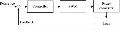
FIGURE 8.1 Schematics of the feedback control loop including a power converter.
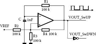
FIGURE 8.2 Simple PWM generator based on operational amplifier.
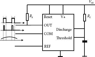
FIGURE 8.3 PWM generator with 555 oscillator.
There are many similar solutions for analog implementation of the PWM controller; all of them work on the principles explained here. The most advanced solutions also include Shutdown pins for each channel in order to discontinue the PWM generation when a fault occurs. Moreover, modern requirements may differ with respect to the power delivered within the PWM signals.
Designed primarily for power supply control, TL5001 from Texas Instruments follows this type of structure, with a dead-time generator and an open collector output transistor able to control the final power-driver stage. Additional features such as under-voltage lockout and short-circuit protection are included.
Given the limited flexibility in changing PWM parameters, these analog-based solutions are hardly used. They still remain a valuable choice in high-frequency servo-drives where the whole controller needs to be implemented in analog due to the extremely high bandwidth required for the control loops. Modern alternatives include high-speed field programmed gate arrays (FPGA) [16] or application-specific integrated circuit (ASIC) devices with predefined control loops and a PWM generator.
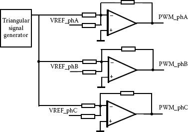
FIGURE 8.4 Schematics of a three-phase PWM generator with unique triangular generator.
8.2 MIXED-MODE MOTOR CONTROLLER ICs
Motor drives in the horsepower range can be controlled with ICs without too many external components. This became a standard requirement for appliances or servo-drives when costs had to be reduced for commercial purposes.
There are many excellent mixed-mode IC-technology solutions in the market. They are designed to control low-voltage motor drives with applications in the automotive and consumer sectors. These controllers incorporate analog controllers, PWM generators with protection and deadtime circuitry, and gate drivers. The most advanced solutions also include power supply for the high-side MOSFET transistor instead of a conventional bootstrap external supply. In several automotive applications, the gate driver needs a separate power supply as the DC bus voltage may decrease below the limit required for proper gate control. For instance, A3948 [1] from Allegro Microsystems includes a boost inductor with three pairs of drivers to maintain gate control voltage.
Control systems are grouped around two application classes: the general brushless DC (BLDC) motor able to provide continuous rotation and the stepper motor able to provide start/stop operation or great positioning. Both provide integrated control solutions in mixed-mode IC technology.
The first generation of step-by-step motor incorporated the PWM current controller and the power stage within the same design, as in the Allegro A3966, in which the required phase reference currents are set by an external reference. Further developments in technology pushed for a complete solution, including a digital-to-analog controller to set current levels (A3967–A3977). The digital interface in these models allows communication with higher hierarchical levels. Further R&D is dedicated to specific applications and it includes transmission of fault conditions over the serial or parallel digital communication interface.
All these solutions are at the edge of IC technology and the future may see new products dedicated to higher power levels or with more digital and analog functions for better protection and control. For the moment, these solutions are limited to the low-voltage converter bus and small power motors.
8.3 DIGITAL STRUCTURES WITH COUNTERS: FPGA IMPLEMENTATION
8.3.1 PRINCIPLE OF DIGITAL PWM CONTROLLERS
The same implementation of a timer followed up by a comparison with the reference signal can be implemented in digital with counters and compare units. Modern microcontrollers have incorporated compare units along their timers/counters that make straightforward the PWM implementation. A single-channel PWM can be implemented with a counter, as in Figure 8.5.
PWM signals for the six switches within a three-phase inverter can be generated in several ways with counters. Generally, one signal is generated for each phase and a complementary pair of signals for the low side or the high side is achieved by a logical inversion. The designer must pay attention to the polarity within the gate driver in order to send the proper control signal to the controlled insulated gate bipolar transistor (IGBT)/MOSFET. As a rule of thumb, the gate drivers used or built in the U.S. generally do not invert the control signal polarity, whereas those made in Europe or Japan do change the control signal polarity. This is why all PWM from microcontrollers initially designed for the Japanese or European markets have negative outputs, expecting the gate driver to reverse the signal polarity.
Finally, the design engineer needs to verify if the digital system can build the deadtime by itself or whether an external deadtime generator is necessary. Sometimes, the gate driver itself is able to generate fixed values of deadtime.
PWM can be generated with counters for a three-phase inverter in one of the following topologies:
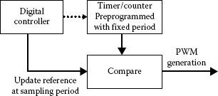
FIGURE 8.5 Principle of counter/timer use in single-channel PWM generation.
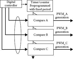
FIGURE 8.6 Three-phase PWM generation with a single counter.
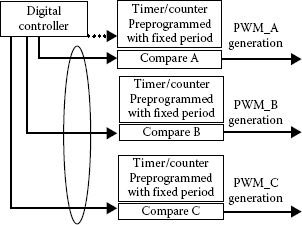
FIGURE 8.7 Three-phase PWM generation with 3 counters and 3 compare.
• A single common counter and three compare units, one for each phase, using the same counting device (Figure 8.6)
• A counter and a compare unit for each individual phase (Figure 8.7)
Depending on the internal structure of each timer, generation of the pulse width can be different. Figure 8.8a shows a left-aligned variable pulse width control, Figure 8.8b a right-aligned PWM, and Figure 8.8c a center-aligned PWM. The last one is a logical result of using the first two solutions back-to-back. Commercially available PWM generator circuits usually implement the center-aligned approach.
Some of the digital PWM ICs have been available in the market since the late 1980 s. Due to simplicity in designing with FPGA and ASIC, these PWM circuits no longer represent an appealing solution, but their principle of implementation can be used as a starting point for modern FPGA [16] or ASIC solutions.
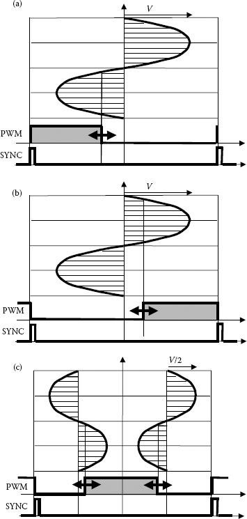
FIGURE 8.8 (a) Left-aligned, (b) right-aligned, and (c) center-aligned PWM.
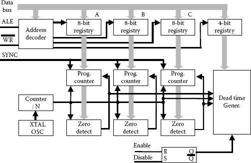
FIGURE 8.9 Block diagram of SLE 4520.
8.3.2 BUS COMPATIBLE DIGITAL PWM INTERFACES
Figure 8.9 shows the block diagram of the Siemens SLE4520 circuit. A similar solution has been implemented by Dynex.
The SLE4520 circuit is designed as an external interface for any 8-bit microcontroller and its operation can be programmed from microcontroller or microprocessor through a data bus and a control signal bus. The time constant or pulse width associated to each phase can be stored within an 8-bit registry and loaded into counters at each SYNC signal. The programmable counters count down to zero when the state of the switching signals for the inverter control change. The deadtime constant can be programmed within a 4-bit registry. When a fault occurs in the power stage, the emergency shutdown pin is activated and it cancels out the PWM signals through the RS flip-flop.
Similar solutions for digital devices able to generate PWM with or without deadtime are developed to directly interface on the data and address bus of modern microprocessors or digital signal processors (DSPs) [20,23,24,25]. The same idea is actually used in custom-made FPGA or ASIC devices, but it is worthwhile quoting more examples of digital devices available for PWM generation from a processor bus.
The IXDP610 from IXYS can provide a single-channel pair PWM control for a switching power converter bridge [21,22]. It has a complete digitally programmable interface from an 8-bit microprocessor. This has a digital comparator, comparing a counting timer with a preprogrammed constant followed by a deadtime generator. The IXDP610 is able to control power PWM devices that have switching frequencies between zero and 390 kHz, 7-bit or 8-bit resolution, and up to 11% deadtime. The output is able to drive directly 20 mA and it is suitable for opto-couplers, gate driver circuits, or low-power power modules. It also features a pulse-by-pulse shutdown protection against over-current, over-voltage or over-temperature, controlled by a logic signal from protection sensors.
8.3.3 FPGA IMPLEMENTATION OF SPACE VECTOR MODULATION CONTROLLERS
Space vector modulation (SVM) represents a special case in which a digital method is required to calculate time intervals to be loaded in counters/timers, followed up by another method able to define the switching sequence. There are numerous solutions possible for digital hardware implementation. One of them is next presented [2] and it considers an SVM generation with only three states during each sampling period (active1—active2—zero state). The following interval will have a reversed sequence (active2—active1—zero state), in which the zero state is always selected with only one switching difference from the last active state.
The memory look-up table can be reduced if we take into consideration the symmetries of the three-phase system as well as the symmetries around the bisectrix of each generalized 60° sector. The most significant bits (MSB) of the angular coordinate reflect the sector number and they are used to select the proper switching sequence in the second memory look-up table. The fourth MSB is used to define the position within each sector and also to establish the sequence of the active states. The last four bits of the angular coordinate are used to read the ta, tb time constants needed for SVM generation. This memory look-up table stores these constants for an interval of 30° only (24 increments within 30°). Each time constant is defined on eight bits and this resolution is considered as enough for this PWM application.
An external periodic signal is used as the system clock and a frequency divider counts the sampling interval period. The definition of the pulse width is limited by having only 28 = 256 points for a sampling interval, as shown in the definition of the memory look-up table. The overflow of the sampling period counter changes the state of a flip-flop D. The outputs of this flip-flop control the sequence of the time intervals ta and tb through two OR gates. Finally, a “switch” module is used to designate the meaning of two signals A1 and A2 corresponding to the different meanings of ta and tb in the first half of the 60° sector and in the second half of the 60° sector. For instance, generation of a position at 23° and a modulation index of 0.6 leads to t1a=ta(V1)=0.36 Ts
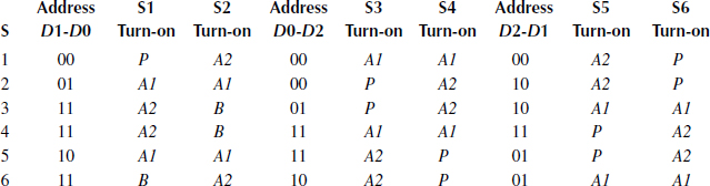
Using two memory look-up tables is not convenient, especially because they are of different sizes. The switching sequence can be defined with a combinatorial circuit and a series of multiplex circuits (Figure 8.10). Observing all the possible switching sequences, the synthesis can be developed as shown in Table 8.1.
Figure 8.11 shows the logic decoder used instead of the memory look-up table and is built up of a divider of six Johnson counters [D0-D1-D2]. The outputs of these counters can be used as addresses for the multiplex circuits having P, A1, and A2 as inputs. Table 8.2 illustrates this decoding of the end of counting signals.
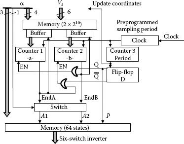
FIGURE 8.10 Principle of pure digital implementation of an SVM algorithm.
Other digital or FPGA syntheses of the SVM algorithm can be found in [3,4,5,6,7]. Many of them implement the SVM algorithm in a straightforward manner with calculation of Equation 5.30 followed by switching sequence decoding. The latter module can be changed from one SVM algorithm to another, for instance, in order to reduce losses (see Chapter 5).
The final stage before firing the gates of the power semiconductor devices is represented by the deadtime generator. The role and calculation of the deadtime interval have been explained in Chapter 3. The deadtime generator is usually implemented together with the PWM algorithm, but special circuits for deadtime generation also exist.
TABLE 8.1
Defining the Switching Sequence from the End of Counting Signals
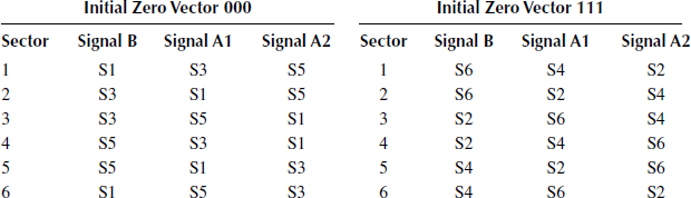
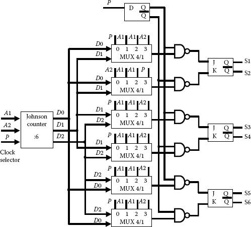
FIGURE 8.11 Example of SVM digital synthesis with multiplex circuits.
TABLE 8.2
Proposed implementation
8.3.4 DEADTIME DIGITAL CONTROLLERS
A solution for deadtime implementation with counters is shown in Figure 8.12 and it corresponds to IXYS circuits IXDP630/631PI [21,22]. The deadtime is always eight clock periods and the clock can be an external crystal or an RC oscillator circuit. Controlling the clock period, one can adjust the deadtime interval. The same IC is able to generate deadtime on all three phases separately. An additional “output enable” signal is able to shutdown all or each output. The operation of this circuit can be understood from Figure 8.12. Each positive edge of the control signal SIN delays the positive edge of the gate signal S_High and each negative edge of the control signal SIN delays the positive edge of the gate signal S_Low. Negative edges of S_High and S_Low directly follow the appropriate edges of the control signals.
8.4 MARKETS FOR GENERAL-PURPOSE AND DEDICATED DIGITAL PROCESSORS
8.4.1 HISTORY OF USING MICROPROCESSORS/MICROCONTROLLERS IN POWER CONVERTER CONTROL
Chapter 1 presented the main control functions required for implementation on the digital control system platform. There are two directions of development in the digital world able to implement all these functions.
The first direction focuses on architectures of general-use microprocessors. These devices achieve incredibly fast running of the control code, and include many functions implemented in the software. The evolution of microprocessors in the last 25 years started with families of bit-slice devices, such as INTEL3000 or AMD2900; 8-bit microprocessors such as INTEL I8080, ZILOG Z80, and I8085; 16-bit microprocessors such as I8086, Z8000, Motorola 68000, and Texas Instruments 16008/16032; and 32-bit microprocessors scuh as 68020 or I80385. They were upgraded in the late 1980 s with arithmetic coprocessors used in tandem, such as INTEL 80826/80287, National Semiconductor NS 32016/32081. This evolutionary step also included other LSI circuits:
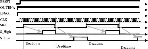
FIGURE 8.12 Time diagram of the deadtime generator circuit IXDP630/631PI.
• High-speed hardware multipliers able to calculate 24 × 24 bits in fixed point in 200 ns, and 16 × 16 in 34 ns (for instance, MPY016 K-TRW)
• Arithmetic modules for calculation in variable points up to 80 bits (e.g., AMD 511, 9512), which work as slave coprocessors to the main microprocessor device
• Multichannel acquisition systems (e.g., AD162, AD364, DAS1150) or dedicated interfaces to existing microcomputers in digital systems, such as INTEL, PROLOG, MOSTEK, TI, or DEC, and so on
• Fast RAM memories, with double port access and huge capacity
• Special digital circuits used to fast interface to microprocessor buses
• Circuits dedicated to generation of the multichannel PWM for control of power converters
• Complex digital circuits containing ROM-I/O-Timer peripherals dedicated to extension of existing microprocessors (e.g., MC6846 used in conjunction with Motorola 6800 device)
In order to fully understand this evolutionary step, let us take an example. Zilog Z80 was a quite widely used 8-bit microprocessor family in the 1980 s. The clock speed was limited to 4 MHz and the peripheral functions were achieved on separate chips from the main device. A special device called PIO-Z80 was dedicated to the parallel I/O, another one to the serial communication SIO-Z80; a special memory access unit DMAC-Z80 and a timer/counter circuit CTC-Z80 completed this family. A fully operational microsystem was required to contain all these ICs on a common printed-circuit board with all the data, control, and address buses accessible from outside. Once this board was realized and tested, coding was done directly on assembly language without any real-time debugger or the possibility to visualize the operation through a monitor program.
All these digital solutions of the late 1980 s or early 1990 s had, however, a quite limited processing speed. Some of them are still in use due to their generality and simplicity. An alternative able to increase the general operation speed considers off-line processing and storage of the control results in a large memory look-up table. The best example is offered by implementation of different PWM algorithms through memory look-up tables. Initially, there was a substantial limitation due to the inherent limited speed of access to these memory look-up tables. Modern ROM devices can achieve access times sufficient for the switching of modern power converters. We will come back to these solutions few years later with the advent of FPGA devices.
The second major direction of development was in modern microcontrollers designed for industrial applications and including dedicated peripherals within the same silicon die. These microcontrollers incorporated on the same chip more memory and I/O interfaces along with their MUX, A/D converters, timers, PWM channels, and so on. Several examples that met with success in the beginning of the 1990 s are still in use today:
• INTEL 8051 (with its versions 8031, 8751, 8052, 8032, and different manufacturers like Siemens or Philips) contains:
• An 8-bit microcomputer with its own clock generator
• A dedicated module for Boolean processing
• kB of ROM (8031 without memory, 8751 equipped with EPROM, and 8052 with 8 kB and a BASIC interpreter)
• 128 bytes RAM (with 256 at 8052)
• Two 16-bit timer/counter circuits (8052 equipped with three such counters) used especially for PWM generation
• Four programmable I/O, bidirectional, with option for each bit to read, write and program
• Serial I/O channels
• Two external interrupt inputs, that can be enabled or disabled by software (8052 equipped with six interrupts including two external inputs)
• Dedicated registers for arithmetic operations, stack management, I/O latches
• A strong assembly language with 111 instructions, enhanced with interpreter for BASIC or PL/M
• INTEL 80186 microcontroller created after the 80196 microprocessor with an architecture similar to the 8086-2 but also including:
• A clock generator at 8 MHz
• Two high-speed Direct Memory Access (DMA) channels
• Programmable interrupt controller with five levels of priorities
• Wait state generator
• Dedicated bus controller
• Possible coprocessor interface
• Software compatible with 8086 and option for programming in ASM86, PL/M86, PASCAL 86, FORTRAN86, LINK86, C, and so on
• INTEL 8096 16-bits microcontroller with enhanced interfaces to analog and digital systems. Different versions include:
• kB or no memory
• Four or eight 10-bits A/D channels with a conversion time of 42 μs
• Five I/O ports
• Serial output port
• One external interrupt
• PWM output
• Four channels for fast capture and event timing with the existing counter
• Six fast outputs programmable to generate pulses at fixed time intervals with a resolution of 2 ms
• Two timers of 16 bits each, one for real-time synchronization and the second for countdown of external events
• Watchdog circuit
• Assembly language with interpreter for PL/M
• Additional microcontroller examples from the same historical class are Motorola MK 68200, MK3870, NEC μPD 78312, INTEL 8748, Philips PCB8049, MAB 4048, and so on.
8.4.2 DSPS USED IN POWER CONVERTER CONTROL
All these efforts to add more functions to microcontroller chips have not been enough for modern applications, and semiconductor engineers have moved forward to DSP devices [20,23,24,25]. DSPs have emerged in the communications business for fast processing of information from data and signals. They are characterized by very quick clock rates and additional processing circuitry within the same chip. It is normal to expect a 16 × 16 multiplication calculated within 100 ns on any of these devices.
Lately, the use of DSPs in power conversion control has been widened by dedicated motor control DSPs equipped with special peripherals designed for multiphase converter control. These devices are generic, are called Motor Control DSPs, and they feature three-phase power conversion PWM control useable in both machine drive and three-phase grid-tied applications. The main DSP producers in the world are—in an arbitrary order—Texas Instruments, Motorola, and Analog Devices. A brief description of the features of each type of DSP and its specifics in controlling three-phase power conversion follows.
The largest DSP market share belongs to Texas Instruments. Their DSPs have passed through a series of iterations and versions in the last 10 years. The TMS320 family of DSPs [23,24,25] is made on a Harvard architecture that allows execution of several operations simultaneously for increased running speed.
The first use of the DSP to control power converters seems to be based on TMS32010/32020, a general use DSP. Its features include:
• Working on 16 bits with an instruction cycle of 160 ns
• A small RAM memory of 144 × 16 bits
• A parallel 16-bit module for a 160 ns multiplication
• Eight I/O ports of 16 bits
• An external interrupt
• Special registers for data processing
• A 16-bit timer
• Interface for memory access in multiprocessor mode
In the early 1990s, Texas Instruments had developed a set of peripherals for motor drive control under the name Event Manager. This was their first generation motor control DSPs, TMS320F(C)24x, and it was optimized in the second generation TMS320F(C)240x that was released in the late 1990s. In 2002, TI released the third generation motor control DSPs, TMS320F(C)280x, which had a very high-speed Central Processing Unit (CPU), able to run programs at a clock frequency of 150 MHz. Section 8.5 will present in detail all hardware and software possibilities for PWM implementation on a TI DSP using the Event Manager.
Analog Devices has another good DSP program with motor control features. Several architecture solutions have been tried and developed at Analog Devices and the most remarkable probably refers to the development of a motor controlled coprocessor. The first solution, called ADMC201, was subsequently developed into ADMC330, ADMC401, and finally incorporated as a peripheral of a DSP circuit within the same package. Section 8.7 will reiterate the historical importance of this architecture development.
The DSP family ADSP-219x represents another solution from Analog Devices with many applications in power electronics [20]. This 16-bit fixed-point DSP core is able to perform 160 MIPS in its modern versions. Other power converter control-related peripherals include:
• On-chip RAM 8 k Words shared between program RAM and data RAM
• External Memory Interface with dedicated Memory DMA Controller for data and instruction transfer
• Eight-channel, 14-bit analog-to-digital converter system with up to 20 MSPS sampling rate
• Three-phase 16-bit center-based PWM generation unit with 12.5 ns resolution at 160 MHz core clock
• Dedicated 32-bit encoder interface with companion encoder event timer
• Dual 16-bit auxiliary PWM outputs
• Three programmable 32-bit timers
• Sixteen general-purpose I/O pins
• SPI and synchronous serial interface
Other DSPs of the same generation are NEC7720, Fujitsu MB8784, and STC-DSP128.
The large number of customers and the extensive use of these DSPs in the world have encouraged development of software libraries dedicated to DSP applications. Programmable in both assembly language and C language, these devices helped develop a software culture and a style for programming proper to motor-drive applications. Recent efforts will probably provide code modularity and automatic software validation. Conventional development tools have been extended in the loop viewers and automatic programming tools. Companies like MathWorks have produced systems able to include the DSP system in a PC-based simulation program for quick development and debugging of new codes dedicated to power converter control.
8.4.3 PARALLEL PROCESSING IN MULTIPROCESSOR STRUCTURES
In parallel with the tremendous development in DSP devices, engineers have tried to use digital systems with parallel processing for control of power converters. These systems allow more processing power even if they do not directly benefit from special peripherals. The whole control algorithm is therefore brought down to the time scale of the PWM algorithm.
The software operation in a multiprocessor system is based on a waiting list for processes, special set of instructions for creation of parallel tasks, a minimal context for fast communication between processes, several timers, and an evolved interrupt system. Selection of the communication protocol between parallel micro-systems is very important and there are several options available: series transfer, parallel transfer through handshaking, DMA transfer, FIFO transfer, double-port RAM memory transfer, and multiple bus architecture.
A device in this category, INMOS Transputer 414, uses for execution reduced instruction set controller processors able to run with 32 bits at 50 ns and to communicate internally at high speed.
The same tendency to use parallel hardware is seen in the development of software platforms. The simplest microprocessors need to model numerous concurrent events sequentially. Assembly language is the quickest way to implement these models, though programs written in assembly language often have sequences that are redundant and too detailed. To simplify this process, many engineers use high-level programming languages like C, PL/M, PASCAL, Visual BASIC, and so on. Programming is therefore reduced to establishing clear tasks and writing special modules for each task. The main program is then grouping these tasks based on priority levels.
The sequential processing of tasks does not extract all benefits from the parallel processor hardware. The first programming language that consistently expressed parallelism in execution was APL [8]. However, the task was computed through computing power distribution, since, at that time, real parallel hardware was not available. The programming language ADA represents an important evolutionary step, especially in conjunction with the specialized 32-bits microprocessor iAPX432. The first truly parallel evaluation of tasks was carried out with the programming language OCCAM, which was able to achieve synchronization and communication between tasks on different hardware. OCCAM is the programming language for transputer, but it can be adapted to any other computer with minimal modifications.
OCCAM shares tasks in individual processes that run separately by communicating between them. The whole program can be seen as a network of interconnected processes. The synchronization between processes requires that all of them run in the time required by the slowest process and that results are reported at each step. Transputer devices simulate this concurrency through software time-slicing, followed by communication through the four serial communication channels. This structure can be extended further, if necessary.
Despite the computing power of these parallel architectures, they are not used in large series production of power converters. Manufacturing operations require a reduced number of terminals to be soldered and a cheap semiconductor solution. Furthermore, firmware considerations also encourage the use of a simpler software-based solution.
8.5 SOFTWARE IMPLEMENTATION IN LOW-COST MICROCONTROLLERS
8.5.1 SOFTWARE MANIPULATION OF COUNTER TIMING
Many microcontrollers do not benefit from a dedicated motor control peripheral and they can implement PWM algorithms using software. A minimal timer is still required for real-time accounting. The software has to calculate the time intervals necessary for the next sampling interval and to sequentially program the timer for each state. Obviously, the resulting PWM cannot have a very large PWM frequency, given the real-time requirements, but it may satisfy many low-cost applications.
Consider an implementation of the conventional SVM algorithm using a single timer circuit and a parallel interface for inverter control. This digital structure imposes some requirements in designing the software controller:
• Each time constant must be calculated by the software on the basis of general SVM relationships. This will limit the maximum frequency of the fundamental waveform able to be generated by this system.
• The timer channel should produce an interrupt at the beginning of each time interval followed by a software compensation for all delays produced by this approach.
• A parallel interface is used to generate the PWM output signals on each interrupt produced by the counter.
A time diagram for this approach is presented in Figure 8.13. Due to the pure software implementation, the switching frequency is limited in the support processor and not too many other features can be run on the same platform. The advantage, however, is an extremely reduced list of hardware requirements: a simple timer and software processing of the comparison result is enough.
This solution is not very practical, though, and another solution is presented in Figure 8.14, in which four timer channels are used for synthesis of each sampling interval. The end of each timing interval produces the start of the following counter and the timing of the next inverter state. The same software structure is required to calculate the PWM.
8.5.2 CALCULATION OF TIME INTERVAL CONSTANTS
The second major requirement to implement a PWM algorithm is that the constants to be loaded within timers for counting the different state intervals must be determined very quickly.
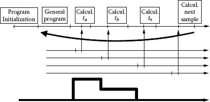
FIGURE 8.13 Time diagram of a pure software implementation of SVM.
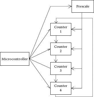
FIGURE 8.14 SVM software implementation based on four counters.
Chapter 5 showed the symmetries in the generation of an SVM algorithm, symmetries after each 60° interval and around the bisectrix of each interval. This can help in reducing the size of the look-up table required to implement the SIN/COS function. Many DSP or microcontroller devices already have in their ROM memory a brief SIN look-up table, usually with 256 or 512 points over a complete cycle. If a higher resolution is required, a new look-up table can be generated by a computational software package like MATLAB or MATHCAD and incorporated with the control program. The number of points within the SIN look-up table determines the resolution in defining each pulse width. This is important for high-switching frequency applications with advanced controlllers. Because memory is not generally a serious constraint, incorporation of a high-resolution SIN look-up table is not a problem in modern microcontrollers.
A totally different approach that is able to take advantage of the computing speed of modern controllers while saving memory requirements is to approximate the reference signals by interpolation. Different mathematical approaches for interpolation are available and they can be used to extend the range of a SIN look-up table from what is already installed in the microcontroller or DSP ROM memory to what the current requirements are to generate the PWM.
An alternative solution to achieving interpolation is fuzzy logic. The theory of fuzzy logic was first proposed in a paper of Professor Lotfi Zadeh in 1965 [9]. For many years this theory was not of interest until, in the 1970s, a series of books extensively presented the mathematical aspects of fuzzy logic [10,11]. In the early 1990s, many papers tried to implement concepts of fuzzy logic in the control of power converters, especially in replacing conventional PI controllers with fuzzy logic controllers. But it did not really succeed in power converter applications, mainly due to existence of other conventional nonlinear control methods and some difficulties in implementation.
A special feature of the fuzzy logic theory was outlined at the 1992 IEEE conference for fuzzy logic systems, where it was repositioned as a logic of interpolate thinking.
This section presents an example of the use of fuzzy logic to implement the interpolation concept, which generates an SVM from a SIN look-up table with a reduced number of points [12,13].
Consider a PWM model with 24 points over the fundamental cycle. The zero states of the model are shared equally during each sampling interval. To simplify the explanation the demonstration is limited to a generalized 60° sector. The fuzzy logic-based control relations can then be expressed as
If α=i*π12⋅ then Ka=Ki with i=0,…,4. |
(8.1) |
This says that for a reduced number of five angular coordinates over the 60° sector, we know precisely what the time constants for each active vector are. The whole set of angular coordinates is therefore described by five fuzzy subsets. Figure 8.15 presents the membership functions for each variable. This choice of the membership functions along with a linear defuzzification method presents less distortions when equivalence with an identical crisp system is sought. Besides, this is very simple to implement. The effect of different approximation approaches in the output phase voltage is shown in Figure 8.16.
The linear defuzzification approach produces a very good interpolative approximation, each harmonic of the output phase voltage having an error below 10−5 of the precise calculation method. This is also reflected in the total harmonic distortion (THD) calculation for the output phase voltage. Figure 8.17 shows the similarity between the two methods.
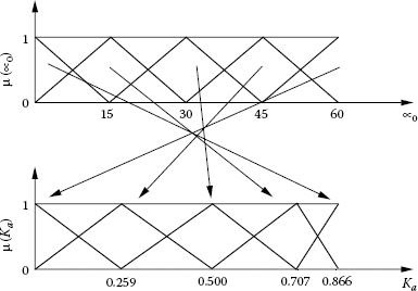
FIGURE 8.15 Fuzzy subsets for the proposed method.
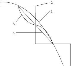
FIGURE 8.16 Effect of different approximation methods in the output phase voltages: (1) sinusoidal PWM; (2) staircase PWM; (3) center-of-gravity defuzzification; and (4) linear defuzzification.
A software implementation algorithm for this method is presented next along with a numerical example:
1. Calculate the polar coordinate of the next desired vector position (Vs, α).
Example: (Vs, α)=(0.45, 212°)
2. Define α0 as the angular coordinate within the generalized sector.
α0=212°–(INT(212/60))60=32°
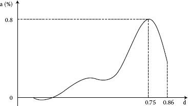
FIGURE 8.17 Relative differences between the two methods.
3. Fuzzy estimation of the time intervals allocated to each active vector Ka, Kb based on α0.
Define the sector number:
I=INT(α/15)+1=3
Calculate the membership degree of α0 to the left subset:
μ1(α0)=(15 * 1–α0)/15=0.86
Calculate the membership degree of α0 to the right subset:
μ2(α0)=1–μ1(α0)=0.14
Calculate the time interval by linear defuzzification:
Ka=(μ1(α0)*KI+μ2(α0)*KI+1)=0.86*0.5+0.14*0.707=0.528
Calculate the second time interval by linear defuzzification:
Kb=(μ1(α0)*K6–I+μ2(α0)*K5–I)=0.86*0.5+0.14*0.259=0.467
4. Determine the actual time constants by multiplication with the sampling interval period.
5. Calculate t01 = 0.5 * (T – ta – tb).
6. Select the appropriate switching pattern (t01 → ta → tb or t01 → tb → ta).
7. Timer programming.
This fuzzy logic-based approach can be extended to V/Hz control of three-phase induction motor drives. The V/Hz characteristic is not linear for the whole range, but requires some nonlinearity in the low-frequency range in order to compensate for the voltage drop on the stator resistances. This nonlinearity can also be mapped with a fuzzy logic-based variable. The resulting controller has two inputs and can be implemented based on the rule table shown in Table 8.3. The linquistic degrees are general without any relationship to their language sense. Each rule can be interpreted as:
IF α is NS (negative small) AND f is PS (positive small), THEN ta is NS (negative small).
The membership functions are considered triangular, symmetrical, with prototypes provided by the time constants calculated for the 24-pulse PWM case. The resulting control surface is shown in Figure 8.18, comparing the ideal and approximate cases.
8.6 MICROCONTROLLERS WITH POWER CONVERTER INTERFACES
Given the large market for low-power motor drives with applications in appliances and servo-drives, some manufacturers have developed microcontrollers dedicated to motor control. The pressure to make these devices low cost is extremely high and giving up features not necessary in basic inverter control applications could make them very competitive. Along with a simple, low-cost 8-bit central processing unit, these devices benefit from dedicated hardware interfaces for PWM generation and A/D conversion and data acquisition. Different communication interfaces complete the internal structure, which is optimized for motor drive applications.
TABLE 8.3
Rule Table for The Fuzzy Logic Controller
αf |
Negative Big (NB) |
Negative Small (NS) |
Positive Small (PS) |
Positive Big (PB) |
Negative big (NB) |
Positive big (PB) |
Positive big (PB) |
Positive medium (PM) |
Negative big (NB) |
Negative medium (NM) |
Positive big (PB) |
Positive medium (PM) |
Zero (Z) |
Negative big (NB) |
Negative small (NS) |
Positive small (PS) |
Zero (Z) |
Negative small (NS) |
Negative big (NB) |
Zero (Z) |
Positive small (PS) |
Zero (Z) |
Negative medium (NM) |
Negative big (NB) |
Positive small (PS) |
Zero (Z) |
Negative small (NS) |
Negative medium (NM) |
Negative big (NB) |
Positive medium (PM) |
Zero (Z) |
Negative small (NS) |
Negative medium (NM) |
Negative big (NB) |
Positive Big (PB) |
Zero (Z) |
Negative small (NS) |
Negative medium (NM) |
Negative big (NB) |
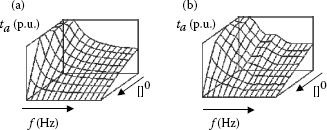
FIGURE 8.18 Controller surfaces: (a) ideal and (b) approximative.
A good example within this category is the NEC μPD78098x [14]. This class of microcontrollers has seven channels of programmable timer/counters for event management along with a low-cost central processing unit running at 8 MHz. Using a 10-bit timer for PWM generation, it has dedicated circuitry able to generate three pairs of output signals (inverter control) and a programmable 8-bit deadtime generator. Eight 10-bit A/D conversion channels are also available for power converter feedback control. A UART communication interface may place this device as a lower level controller in a hierarchical structure.
Because of the limited clock frequency (8 MHz), the PWM cannot be generated with a carrier frequency of 15.6 kHz (64 μs) or higher when the timer is programmed to an 8-bit resolution or on 3.9 kHz (256 μs) for the 10-bit resolution. The clock frequency is scaled for different switching frequencies below these values. For higher switching frequencies, the 8-bit or 10-bit resolution cannot be achieved, and the timer should work with multiple interrupts from the same timer and should divide the frequency by an appropriate value.
Motorola provides a similar device that can run at up to 32 MHz, and that has a fault-tolerant PWM controller for motor drive applications. The Motorola 68HC08 family also includes a deadtime generator and an interesting deadtime compensation capability [27,28]. These are created around the so-called Timer Interface Module, which also provides capture features. Finally, this device includes USB, CAN, and SPI interfaces with plans for a local interconnect network. As in many modern microcontrollers or DSPs, it has an in-circuit flash option.
8.7 MOTOR CONTROL COPROCESSORS
Any digital feedback control solution can be implemented into a general-purpose processing unit, but the particular control and measurement of a power electronics system requires special peripherals. Current research is aimed at improving the performance of power-dedicated peripherals, and placing it along with the main computing unit.
Another direction of research is toward application-specific peripherals outside of the main processing unit in the form of a digital coprocessor [15].
Analog Devices’ ADMC201/./331 is the most well-known commercial solution using this approach. Developed for motor control applications, it has modular blocks that implement the vector control method within the same programmable digital system. Developed initially as a partner for ADSP2105, it is used in conjunction with other DSPs or microcontrollers as well.
The latest descendent of this family has been incorporated along a 26 MIPS fixed-point central processing unit within the ADMC401. It includes:
• Eight-channel simultaneous sampling A/D converters
• Three-phase 16-bit PWM generator
• Two 8-bit auxiliary PWM outputs
• Park direct and reverse digital transform based on angular coordinates
ADMC331 includes predefined hardware mathematical functions used in motor control, such as vector transforms based on angular coordinates. Hardware based vector transforms provide substantial time saving in a three-phase system control. The feedback control loops can run at higher rates implementing control loops with larger bandwidth.
More recently, International Rectifier developed a similar device (Accelerator TM) able to provide a feedback control loop with a bandwidth of 5 kHz by using FPGA support [15]. Again, all elements of a vector control algorithm were included in VHDL models and implemented within a flexible FPGA structure, providing fast parallel processing of the field orientation algorithm. The system makes possible code modularity and portability for specific applications. This digital system is designed to sit on the DC power bus and to directly control the power device’s gate circuitry. Isolation of the communication interface with the higher hierarchical level is provided.
8.8 USING THE EVENT MANAGER WITHIN TEXAS INSTRUMENT’S DSPS
Texas Instrument’s has manufactured a set of DSP devices dedicated to motor control applications. The particular peripheral module of these DSPs is called Event Manager and it has all functions necessary for motor control. There are slight differences between the Event Manager included in the ‘24x device, ‘24xx device, and ‘280x device, but all are meant to help power converter control. We refer to the Event Manager from the ‘24xx devices only noting slight differences where possible. The ‘24xx series was the most used in early 2000s.
There are two Event Managers within the ‘24xx device, each including:
• Two general-purpose timers that are used to implement different PWM algorithms, quadrature encoder or generation of the sampling period for different control systems. They can work on the DSP clock or on an external clock and can have programmable periods and counting directions. There are local programmable compare modules able to detect a time moment and to release an interrupt or to set an output. An interesting feature allows starting A/D conversion synchronized with a timer operation.
• Three compare units that direct PWM generation by comparing timer values and predefined time constants. Each compare unit has two associated PWM outputs, working on a time base provided by one of the timers. Outputs of the compare units can be programmed easily for different purposes, including carrier-based PWM generation or hardware SVM generation.
• PWM circuitry that include:
• A hardware SVM state machine used for hardware implementation of one version of the SVM algorithm
• Symmetrical or asymmetrical PWM generators
• Programmable deadtime generator
• Programmable output logic
− Three capture units that have two-level deep memory FIFO stacks, able to provide a time stamp for external events, useful in synchronization of events.
− Quadrature encoder pulse circuit used to interface with encoder sensors. It is able to decode and count the quadrature encoder pulses from an optical encoder.
− Interrupt logic and interface with the central processing module. A special power drive protection interrupt logic is included for fast shutdown of the PWM and power stage.
The Event Manager included in the ‘24x device was more complex and had additional functions. However, these functions were not used much and were replaced by other implementation alternatives.
8.8.2 SOFTWARE IMPLEMENTATION OF CARRIER-BASED PWM
Chapter 3 presented different carrier-based PWM algorithms. Their implementation is straightforward with a comparison of the reference signal with a triangular high-frequency waveform. The triangular waveform can be generated with a General-Purpose Timer programmed with the sampling interval period. Each of the continuous counting up, counting down, or up- and down-counting modes may be used resulting in asymmetrical or symmetrical PWM generation. The comparison with the reference is ensured by the three available compare units, each one already tied within the Event Manager to a pair of PWM outputs. The compare units are updated at each sampling interval interrupt. The time intervals to be uploaded into the compare units of the Event Manager are centered around the constant corresponding to half of the sampling interval.
For instance, in order to implement a sinusoidal PWM with subunitary modulation index m and a sampling interval Ts, the period register of the general-purpose timer should be programmed with the integer N_Ts corresponding to the sampling interval, and each compare unit should be updated with
{N−Ta=12N−Ts [1 + m sin α]N−Tb=12N−Ts [1 + m sin (α+2π3)]N−TC=12N−Ts [1 + m sin (α+4π3)] |
(8.2) |
where α is calculated in increments depending on the sampling period and the fundamental period.
8.8.3 SOFTWARE IMPLEMENTATION OF SVM
The simplest solution for software-based implementation of the SVM algorithm on the Event Manager of Texas Instruments’ DSPs is to use the symmetrical PWM-generation feature previously described in Section 8.8.2. The ON-time intervals for each switch can be calculated based on Equations 5.41, 5.42, 5.43, 5.44, 5.45, 5.46 and on the proper definition of the switching reference function. Each sector has the option to generate a switching pattern starting from the zero vector 000 or from the zero vector 111. This can be programmed by selecting the polarity of the PWM output signals. Figure 8.3 is an example of SVM generation of a vector position within the first 60° sector, using active vectors 100 and 110.
The time constants used within the PWM generation on the first 60° sector with compare modules are (Equations 8.3 and 8.4):
When starting from 000:
{N−Ta=T04N−Tb=T04+T12N−TC=T04+T12+T22 |
(8.3) |
where T1 and T2 are calculated using Equations 5.41, 5.42, 5.43, 5.44, 5.45, 5.46 and T0 using Equation 5.47.
When starting from 111:
{N−Ta=T04+T12+T22N−Tb=T04+T12N−TC=T04 |
(8.4) |
where T1 and T2 are calculated with Equations 5.41, 5.42, 5.43, 5.44, 5.45, 5.46 and T0 with Equation 5.47.
A different set of equations should be calculated for each 60° sector. The software routine for SVM generation also requires the proper selection and programming of the first zero vector used for each sector. Because this implementation uses both zero vectors on each sampling interval, all the sampling intervals over one fundamental frequency cycle can be programmed to start from the same zero vector, either 000 or 111. No additional programming is required on each sampling interval but for the change of the time constants within the compare units.
Similar implementations based on the reference function can be conceived with a timer that counts up or down.
8.8.4 HARDWARE IMPLEMENTATION OF SVM
The Event Manager provides a hardware solution to implement the SVM. The user has to program the required polarity of the output PWM signals to enable the hardware implementation of the SVM and to start a general-purpose timer in the continuous up- or down-counting modes.
At each sampling interval, the appropriate interrupt routine has to receive or calculate the vector coordinates of the desired position of the voltage vector (Vd, Vq) to define the sector the vector belongs to. Each sector is characterized by two adjacent vectors Vx and Vx+60 and they are programmed with the calculated vector codes in the Event Manager. Note that Texas Instruments’ code programming definition of the sectors is the reverse of the convention used in this book. The hardware SVM generator also provides an option to select the vector to be used first in the sampling interval. The Event Manager will next use the switching pattern corresponding to these vectors for specified amounts of time.
The user software has to calculate the time intervals allocated to the first (T1) and the second (T2) active vectors on the sector as well as the time interval required for the zero state (T0). Section 8.5 gives some hints to implement this calculation. The resulting constants are loaded as 0.5 * T1 in the first compare unit and 0.5 * (T1 + T2) in the second compare unit.
At the beginning of each sampling period the outputs are compared to the switching pattern representing the first preprogrammed active vector. We get the first compare match at 0.5 * T1 from the beginning of the timer up counting. The outputs are switched to the pattern corresponding to either Vx, if this is selected as the first vector on the sector, or Vx+60, if this is selected as the second vector on the sector.
At the second compare match, at 0.5 * (T1 + T2), the pattern is switched to a zero vector (000 or 111), whichever is closer to the last active vector (or switching pattern). The timer continues to count up to the programmed period, then slopes downwards, counting down. The next match occurs for the compare register loaded with 0.5 * (T1 + T2). This is used to enable the switching pattern for the “second” active vector. At the second match of the slope counting down, the switching pattern of the “first” active vector is transferred to the outputs.
The resulting waveforms are symmetric with respect to the middle of the sampling period. Figure 8.19 shows the two possible ways to generate a vector within the first sector (active vectors 100 and 110) while using the hardware generator within the Event Manager (Figure 8.20). Switching patterns only for the high-side IGBTs are shown. Low-side IGBTs are controlled in a complementary mode.
Notice that only a zero vector is used on each sampling interval, allowing the use of same zero vector for a whole 60° sector. The first consequence relates to lack of switching on one of the inverter legs for 60° and this reduces switching losses. In other words, the hardware implementation of the SVM method within the Event Manager represents a reduced-loss PWM algorithm, suitable for motor control, in which current usually lags behind the voltage. This method (Method DD1) has been already analyzed in Chapter 5, Figure 5.26. At the price of some extra switchings per fundamental period, other reduced-loss SVM algorithms may be implemented on the same hardware.
A deadtime generator is also included within the Event Manager. A single value should be programmed for all six outputs and if the deadtime generator is enabled, the rise-up (turn-ON) of each of the output signals is delayed by a preprogrammed time interval. The deadtime interval depends on clock period, clock prescaling, and the 4-bits programming constant covering all time intervals required by modern power semiconductors.
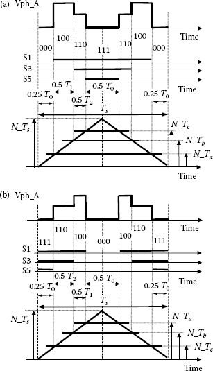
FIGURE 8.19 Example of vector synthesis using the hardware SVM generator. (a) Starting the sampling interval with 100. (b) Starting the sampling interval with 110.
Texas Instruments’ DSPs also include several PWM channels able to work individually directly from a timer. The procedure for programming each individual PWM channel is very easy, starting from setting up a timer as the period counter and loading a compare constant in a special register. When the timer reaches the value preloaded within the compare register, an interrupt can be generated and an output toggles.
Any new development and implementation of the PWM generators follow the development in digital hardware technologies. One of the most important achievements over the last 5 years was the explosion of the flash memory technology [30,31] and it created a new implementation opportunity for the PWM generators [34].
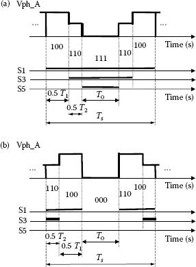
FIGURE 8.20 Example of vector synthesis using the hardware SVM generator.
Flash memory is a nonvolatile memory that can be electrically erased and reprogrammed. It provides a lower cost with more functionality than previous technologies for nonvolatile memory. The first flash memory device was invented in 1981 by Fujio Masuoka at Toshiba Corporation. The technology has been adopted steadily since then, topping $20B in 2006, which meant 34% of the entire market of memory devices. Later on, it went up to 50% of the entire memory market.
The success of the flash memory technology reflected in the control of power converters as well. The 2011 generation of power conversion microcontrollers (formerly known as “Motor Control DSPs”) are introducing more on-chip flash memory as well as DMA (Direct Memory Access) circuitry [32,33]. The principles of using DMA circuitry in power conversion control is known from the early 1980 s [35] when external DMA interface circuits were paired with microcontrollers for better memory access. However, the microcontroller devices did not use this feature too much until 2011. Now, both the TI’s Piccolo series and the Zilog’s Z16FMC series are introducing DMA control for both internal and external flash memory [32,33].
Another recent technology development is related to access to external large-size flash memory with improved single-, dual-, or quad-I/O SPI interfaces. The Serial Peripheral Interface principles are known for quite a while, and this serial communication interface is mostly used as a simpler alternative to more complex solutions like RS232, RS485, and so on. The baud-rate yields limited by its 1-bit serial transfer of information. The newer versions extend the same principle to communication on 2 or 4 wires along with the appropriate communication management. The speed can be thus increased up to 320 MHz by sending and receiving 2 or 4 bits of data at a time.
The use of flash memory within the digital control platforms benefits from the principles shown previously in Section 3.7 as binary programming PWM. Instead of the conventional comparison of a reference with a carrier signal implemented on different timer structures, the novel approach uses optimized PWM stored in large look-up tables. This allows complex optimization at the pulse level otherwise impossible to be achieved within power converter products.
Numerous algorithms for PWM optimization are reported over the last 30 years. They were not very successful in industrial application due to the extensive digital resources necessary for implementation as well as the somewhat reduced generality. Extensive memory look-up tables can be nowadays implemented within flash memory, independent of the control system. Moreover, synchronized sampling at various frequencies is possible within the same peripheral.
A novel architecture involving flash memories is proposed in [34] and shown in Figure 8.21. Flash memory chips are organized in 2n blocks, each made up of 2m sectors, each made up of 2q pages of memory. The 2-axis output of the control system provides the start address for a memory look-up table containing a table of 128 words of 8-bit, each of them defining the inverter state at a given moment of time. Similar to the binary programmed PWM presented in Section 3.7, this table is read with a constant clock frequency, and the data is transferred to the 6 gate drivers of the three-phase power converter.
The solution shown in Figure 8.21 [34] is based on a 64MB flash memory. As of 2012, external flash memory chips at $2 are available from companies like Numonyx (M29W640), ST-Microelectronics (SST25VFO64C), Spansion (MirrorBit 64). This low-cost compares to that of stand-alone bus compatible PWM interfaces like Siemens SLE4520 and Ixys IXDP610 [21,22], or companion FPGAs [16].
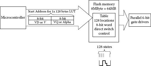
FIGURE 8.21 Hardware architecture with flash memory.
Alternatively, complete PLC and FPGA solutions can be considered to include control logic and memory-based PWM generators within the same device.
The emerging flash memory technology provides an opportunity for the power conversion control designer to reconsider the PWM generation. It is our conclusion that the optimal PWM algorithms previously reported in academic laboratories become now more viable for industrial success with flash memories.
The specific of the new architecture is that either the DMA circuitry or the multi-I/O SPI protocols allow reading a 128-word page of data with a start address only, independent of the microcontroller software run. Contrary to the organization and operation of conventional memory look-up tables where reading each location needs microcontroller intervention, the (vd,vq) address is sent to the memory only once as a start address, and the entire 128-words PWM sequence is transferred to the gate drivers without other intervention of the main microcontroller.
This allows a large variety of state sequences over the sampling frequency that corresponds to the 128 clock periods. Within the conventional PWM generators, the sequence of states over a sampling period is the same over the entire fundamental cycle. As shown in Section 4.2, the state sequence is derived from operation of counters as up-counting, down-counting, or up/down-counting. Previous solutions also agree on the use of 4 states over the sampling period like [zero state -> active vector 1 -> active vector 2 -> zero state], for the entire fundamental cycle. The novel architecture eliminates such limitation.
Possible criteria to be considered for optimization of the PWM waveforms follow the previous sections and are not detailed herein:
• Optimal sharing of the zero sequence states (as demonstrated in Figures 5.17 and 5.18)
• Variation of the pulse frequency by alternating the use of 3, 4, or 5 identical pulses for each position within a 60° sector, depending on the angular coordinate
• Over-modulation based on optimal pattern
As shown within the previous chapters of the book, these criteria are independent of each other and the same look-up table can be used at different fundamental frequencies, different clock frequencies, or different operation points. The use of these optimization criteria within PWM generators leads to the results incorporated in Figure 8.22.
8.10 ABOUT RESOLUTION AND ACCURACY OF PWM IMPLEMENTATION
Given the large number of digital platforms able to accommodate the implementation of PWM generators, it is worthwhile to master the specifics of accuracy and resolution for PWM algorithms. Let us explain these for the two major types of implementation: counter-based and memory-based. Since we limit our discussion to the core PWM generator, we will consider the counter-based structure as generic for any digital implementation, including DSP and PLC/FPGA solutions.
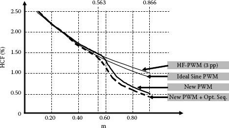
FIGURE 8.22 HCF for 3.6 kHz switching frequency and the optimal PWM.
Most of PLC/FPGA solutions used to implement the PWM algorithms follow the same counter-based structure as the microcontrollers [7,8,9,10,11]. PLC/FPGA(s) offer a higher level of parallelism than microcontrollers [11], and this is used for implementation of faster protection and compensation algorithms like current-based dead-time compensators, or deadbeat current control for bandwidth challenged applications. Such features do not interfere with the core counter-based implementation of the PWM algorithms.
By definition, the resolution of a PWM generator represents the smallest change it can detect in the ideal reference it is provided. Due to the counter-based implementation, modern microcontrollers measure resolution as time increments. High resolution PWM channels go down to 150 ps, and this is most useable for switching frequencies above 200 kHz. Typically, operation within 1–25 kHz does not require high resolution PWM. For instance, a TMS320x280x microcontroller with a system clock of 100 MHz can generate 20 kHz PWM with 12.3 bits resolution on regular PWM, and 18.1 bits on high resolution PWM mode [35].
Limit cycles in voltage-controlled high frequency power supplies may result from the signal quantization and refer to steady-state output oscillations at frequencies lower than the converter switching frequency [36]. This is not the usual case in three-phase converters (open-loop or current controlled) since the current/voltage ripple is way larger than the measurement resolution, and the uncertainty is given by harmonics/ripple rather than by quantization.
The comparison is schematically shown in Figure 8.23.
Figure 8.24 shows that reproducing a sine-wave reference on 12 and respectively 8 bits, in order to generate PWM at 3.6 kHz (72 pulses per 50 Hz fundamental period) produces comparable results in the output voltage due to low-frequency sampling.
By definition, the accuracy of a PWM generator is the degree of closeness of the generated pulse to the actual desired value. The physical size of the memory look-up table limits the accuracy for the memory-based PWM implementation. What is considered today a feasible solution based on widely available and affordable flash memories of 64 MB allows an accuracy of 0.4%. Larger memory devices with appropriate faster access will emerge to better carry on the implementation of the memory-based PWM generator architecture with multiple optimization criteria.
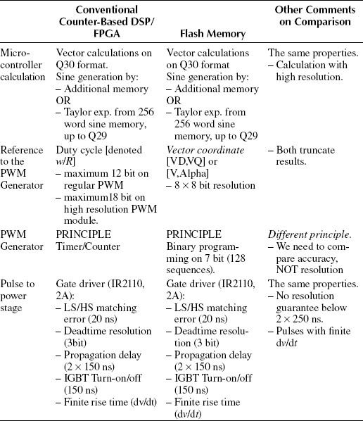
FIGURE 8.23 Comparison of two methods.
This chapter presented the trends in the control of medium and high-power converters. Different theoretical principles for defining a PWM channel by analog or digital means were introduced along with various implementation solutions using modern microcontrollers and DSPs. This chapter is rich in presenting novel solutions to a state-of-the-art power converter control structure.
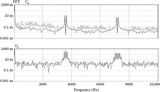
FIGURE 8.24 The effect of quantization resolution on harmonics: top figure = sinusoidal reference quantized on 12, respectively, 8 bits, and sampled at 3.6 kHz by software program; bottom figure = output PWM voltage for a single leg converter, at 50 Hz fundamental, with a reference quantized on 12, respectively, 8 bits, and sampled at 3.6 kHz.
1. Bob, C. 2003. Getting more out of your motor—Motor driver ICs integrate more functions. Allegro Microsystems, Application Note.
2. Neacsu, D.O. 1993. A new digital controller for SVM algorithms. IEEE SCS, 1, 101–104.
3. Tzou, Y.Y. and Hsu, H.J. 1998. FPGA realization of space-vector PWM control IC for three-phase PWM inverters. IEEE Trans. PE, 12(6), 953–963.
4. Sangchai, W., Wiangtong, T., and Lumyong, P. 2000. FPGA-based IC design for 3-phase PWM inverter with optimized space vector modulation schemes. IEEE Midwest Symposium on CAS2000, pp. 106–109.
5. Deng, D., Chen, S., and Joos, G. 2001. FPGA implementation of PWM pattern generators for PWM invertors. Canadian Conference on Electrical and Computer Engineering, pp. 225–230.
6. Tonelli, M., Battaiotto, P., and Valla, M.I. 2001. FPGA implementation of a universal space vector modulator. IEEE IECON, pp. 1172–1178.
7. Cirstea, M., Aounis, A., McCormick, M., and Urwin, P. 2001. Vector control system design and analysis using VHDL (for induction motors). IEEE PESC, pp. 81–84.
8. Iverson, K.E. 1962. A Programming Language, John Wiley and Sons, New York.
9. Zadeh, L.A. 1965. Fuzzy sets. Inf. Control 8, 338–353.
10. Negoita, C.V. and Ralescu, D.A. 1975. Applications of Fuzzy Sets to Systems Analysis. Birkhauser Verlag and New York Halsted Press, Basel.
11. Mamdani, E.H. and Assilian, S. 1974. An experiment in linguistic synthesis with a fuzzy logic controller. Int. J. Man Mach. Stud. 7, 1–13.
12. Neacsu, D., Stincescu, R., Raducanu, I., and Donescu, V. 1994. Fuzzy logic control of a PWM V/f inverter-fed drive. ICEM’94, Paris, France, vol. III, pp. 12–18.
13. Saetieo, S. and Torrey, D. 1998. Fuzzy logic control of a space vector PWM current regulator for three-phase power converter. IEEE Trans. PE 13, 419–426.
14. Anon. 2000. NEC 78098x MCU, NEC, Datasheet Document No. U12804EJ2V1DS00 (2nd edition). Published February 2000.
15. Moynihan, F. 2000. Fundamentals of DSP-based control for AC machines. Analog Dialogue, 34(1), 334.
16. Takahashi, T. 2001. FPGA-based high performance AC servo motor drive—Accelerator TM configurable servo drive design platform. International Rectifier.
17. Mohan, N., Undeland, T., and Robbins, W. 2002. Power Electronics, 3rd edition. John Wiley and Sons, New York.
18. Thorborg, K. 1988. Power Electronics. Prentice Hall, London, UK.
19. Holtz, J. 1992. Pulsewidth modulation—A survey. IEEE Trans. IE 39, 410–420.
20. Anon. 2003. Mixed signal DSP controller ADSP-21990. Analog devices. Datasheet.
21. Anon. 1998. Inverter Interface and Digital Deadtime Generator for 3-Phase PWM Controls, IXYS Datasheet Documentation, pp. 1–20.
22. Anon. 2001. Bus compatible digital PWM controller. IXYS IXDP610 Documentation.
23. Anon. 2001. TMS320LF/LC240xA DSP Controllers Reference Guide—System and Peripherals. TI Literature no. SPRU357B.
24. Yu, Z. 1999. Space Vector PWM with TMS320C24x/F24x using hardware and software determined switching patterns. TI Literature no. SPRA524, March 1999.
25. Doval-Gandoy, J., Iglesias, A., Castro, C., and Penalver, C.M. 1999. Three alternatives for implementing space vector modulation with the DSP TMS320F240. IEEE PESC.
26. Trzynadlowski, A.M. 1994. The Field Orientation Principle in Control of Induction Motors. Kluwer, Dordrecht.
27. Anon. 2001. DSP56301 User’s Manual—24-Bit Digital Signal Processor, Motorola Documentation no. DSP56301UM/AD, Revision 3, March 2001.
28. Anon. 2001. MC68HC908MR32 & MC68HC908MR16 Advance Information—HCMOS Microcontroller Unit, Motorola Documentation no. MC68HC908MR32/D, Rev. December 2001. REV 5.
29. Neacsu, D. 2005. Implementation of PWM algorithms. IEEE PESC.
30. Yinug, F. 2007. The rise of the flash memory market: Its impact on firm behavior and global semiconductor trade patterns. US International Trade Commission, Journal of International Commerce and Economics, Internet Version, July 2007, pp. 137–185.
31. Zitlaw, C. 2011. The future of NOR flash memory. EE Times, May.
32. Anon. 2011. Piccolo Microcontrollers. Texas Instruments Corp., March.
33. Anon. 2011. Motor Control MCUs Z16FMC Series Product Specification. Zilog Corporation.
34. Neacsu, D.O. 2012. Novel microcontrollers with direct access to flash memory benefit implementation of multi-optimal space vector modulation. IEEE Trans. Industrial Informat. 8(3), 528–535.
35. Rajashekara, K.S., Vithayathil, J. 1982. Microprocessor based sinusoidal PWM inverter by DMA transfer. IEEE Trans. IE 29(1), 46–51.
36. Anon. 2011. TMS320x280x—High Resolution PWM—Reference Guide. TI literature SPRU924F, Revised, October.
37. Peterchev, A., Sanders, S. 2003. Quantization resolution and limit cycling in digitally controlled PWM converters. IEEE Trans. PE, 18(1), 301–308.