
10.1 MARKET AND TECHNOLOGY CONSIDERATIONS
Currently, most power converter products are already well defined and accepted by many customers. Hence, the corporate effort is to produce it cheaper and more efficiently by excellence in operations. The process of improving the well-known topologies into fabrication is based on new packaging methods for the hardware as well as novel control architectures and platforms. Moreover, both the fabrication process and the component selection within the design process are now highly optimized.
Different R&D institutions have adopted this philosophy and embarked in product optimization. For instance, the Office of Naval Research (ONR)—a top research sponsorship institution of the U.S. Department of Defense—has sponsored and led a series of programs in mid-1990s and early 2000s meant to demonstrate and improve capabilities in power conversion with focus on packaging, power density, and control architecture. The two major programs including both academia and industry were the Power Electronics Building Block (PEBB) and later the Advanced Electrical Power Systems (AEPS).
Despite targeting mostly naval applications, these programs set-up the basis of standardization and packaging for any medium power application (tens to hundred kW). Later on, ABB has extended the PEBB program into the multimegawatt range. More recently, different aviation electronics producers adopted PEBB as a technology of choice for the development of future more-electric aircraft systems.
In early and mid-2000, ideas that emerged from the PEBB and AEPS programs were assimilated by large power semiconductor manufacturers and designed-into the development of Intelligent Power Modules. The basic description of these IPM devices follows herein, while Chapter 18 a will enter an advanced research topic for developing novel technologies and circuits based on these IPM devices.
The IC technology has experienced an impressive development during the last 30 years. The number of transistors on the same chip has continuously doubled at each other year. This tremendous technology capacity combined with the progress in computer aided-design has allowed emergence of very-large-scale integrated circuits (VLSI) able to achieve high performance in signal processing and size reduction of the electronics equipment.
Similar advancements were possible within the collateral efforts of the power semiconductor manufacturers. Progress has been achieved in packaging of the gate driver, sensing logic, and power semiconductor under the same hybrid IC package. This emerged into a new set of devices—often called “intelligent power modules”—that steadily reached a certain standard of usage in low power range (Figures 10.1 and 10.2). These IPM devices contain a full gate driver with sensing and protection capabilities [1,2].
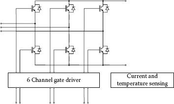
FIGURE 10.1 Typical circuitry within an IPM device.
10.1.2 ADVANTAGES AND DRAWBACKS
Advantages of the IPM-type devices consist of
• Improved reliability since the power semiconductor module could contribute better performance for the system’s reliability than individual components [19].
• Improved reliability since a power module provides a better thermal design and layout, both with effects on the system reliability. Using a power module supplied by manufacturer rather than multiple individual components is recommended for the inverter application [19].
• Two to three times better power cycling capability than using conventional power switches.
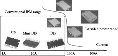
FIGURE 10.2 Examples of packages and power rating for IPM devices.
• Lower parasitic inductance than within the discrete solutions with benefits in voltage spike reduction, and possible operation at higher switching frequency with lower switching loss.
• Simplified power connection (VDC +, VDC−, A,B,C).
• Microcontroller connection through 6 logic-level inputs.
• Propagation delays for all low-side and high-side IGBTs are matched.
• Protection against over-current and over-temperature faults is secured.
• Reduction of system’s volume and weight.
• Easier debugging and field repair of the electronics equipment.
The drawbacks of IPM modules are
• Maximum power ratings were reduced up to recent products.
• Switching frequency is limited due to thermal constraints.
• Still require DC bus capacitor and passive filtering since these modules follow the conventional back-to-back topology.
Performance improvement when using IPM devices instead of discrete devices came from a series of technology achievements such as:
• IGBT device technology –> reduction of power loss.
• Packaging materials –> better heat extraction.
• Improved gate driver control.
Recent IGBT devices aim to deliver benchmark VCE(ON), with zero temperature coefficient, at lowest conduction loss possible, together with soft switching transients able to reduce EMI. The IGBT technology evolved sub sequentially since early 1990s as it follows:
• Punch-through planar IGBT
• Suitable for voltages 250 V–1200 V,
• Cost effective technology, optimized for either speed or short-circuit rating up to 10 μs.
• Nonpunch-through planar IGBT
• Suitable for voltages 600 V–1200 V,
• Optimized for ruggedness,
• Short-circuit tolerance up to 10 μs at higher switching frequency.
• Field-stop trench IGBT
• Suitable for voltages 350 V–650 V,
• Optimized for both conduction and switching performance,
• Rated for 5 μs short-circuit capability,
• Allows higher current rating in smaller packages.
• Punch-through trench IGBT
• Suitable for voltages 600 V
• Cost effective technology at low switching frequencies (below 1–5 kHz),
• Rated for 3 μs short-circuit capability,
• Allows higher current rating in smaller packages.
• Field-stop trench IGBT
• Excellent conduction and switching characteristics,
• Rated for 10 μs short-circuit capability,
• Allows higher current rating in smaller packages.
Different manufacturers have marketed technologies similar with each other, with small variations from this historical evolution. The multiple options for technology development allowed the specialization of the IGBT chip depending on application. The IPM devices emerged first for application to appliance and “white goods” products. The application is therein a motor drive that does not need a switching frequency higher than 5 kHz, with transitions generally below 5 kV/μs (or 5 V/ns). Hence with the main focus of the design process yields on reduction of the conduction loss.
In order to get the most benefit from these new IGBT chips, the gate driver itself is optimized. The gate driver ICs aiming at improved performance are using at least different gate resistors for turn-on and turn-off. The most advanced devices are also considering dynamic control of the transition slope on dependence of the switched current [3,4,5]. Since the gate driver can change its driving speed based on the switching current as discussed in Chapter 2.5, it is possible to achieve simultaneously low loss and low noise (Figures 10.3 and 10.4).
The third key technological advent that made IPM success possible relates to package fabrication (Figure 10.2).
The transfer mold technology was first used and it is based on copper lead frames. For larger power levels, the requirements for heat extraction are more demanding and the heat transfer through the copper leads was not enough. A step forward came with integration of cooling structures like mold resin and aluminum heat-sink. Further on, higher power levels require even more heat extraction which is nowadays possible with integrated ceramic substrates.
As opposed to the low-power IC technology, the substrate of a power module must carry higher currents, provide larger voltage insulation, and deal with increased amount of power loss and heat. The role of the substrate in a power module is to provide the circuit connections and to provide cooling since it is common for the substrate to face operation up to 150° or 200°C. The most used substrate technologies are the Direct Bonded Copper substrate, and the Insulated Metal Substrate.
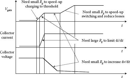
FIGURE 10.3 Nonlinear gate resistance.
Direct Bonded Copper (DBC) substrates are composed of a ceramic tile like alumina and a sheet of copper bonded to one or both sides. The copper and ceramic tile are heated to a controlled temperature, in an atmosphere of nitrogen and oxygen, until a copper-oxygen eutectic forms which bonds successfully both to copper and the oxides used as substrates. The top copper layer can use printed circuit board technology to draw an electrical circuit, while the bottom copper layer is usually kept plain for cooling by attachment to a heat spreader or heat-sink.
The advantages of Direct Bonded Copper technology are
• Low coefficient of thermal expansion, which ensures good thermal cycling performances (up to 50,000 cycles)
• Excellent electrical insulation
• Good heat spreading characteristics
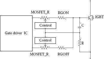
FIGURE 10.4 Possible implementation of the controlled (nonlinear) gate resistance.
The ceramic material used within Direct Bonded Copper technology can be:
• Alumina (Al2O3) = widely used because of its low cost despite the lower thermal performance (24-28 W/mK) and despite being somewhat brittle. Over the years, the thickness of this substrate was reduced from 0.63 to 0.38 mm for most applications in order to reduce the thermal resistance (Rth) from the semiconductor chip to the heat sink.
• Aluminum nitride (AlN) = offers better thermal performance (> 150 W/mK) at higher cost.
• Beryllium oxide (BeO) = despite representing another option for good thermal performance, it is not very much used since it is somewhat toxic.
Insulated metal substrate (IMS) technology starts from a metal base-plate like aluminum, covered with a thin layer of dielectric like an epoxy-based layer, followed by a layer of copper (35 μm to more than 200 μm thick). Due to this structure, the Insulated metal substrate (IMS) technology is a single-sided substrate and it can accommodate components on the copper side only.
Power modules can be designed with or without a base-plate. If the base-plate is missing, the Direct Bonded Copper (DBC) substrate is directly placed on the heatsink. Alternative solutions for the copper base-plate include composite materials such as AlSiC or Cu-Mo, mostly used in traction applications due to their low thermal conductivity and high costs.
The heat removal performance is obviously related to the performance of the materials used for packaging of the power modules. Consequently, the development and improvement of new materials influence size and weight of the power semiconductor modules. Therefore, the contemporary R&D effort is dedicated to justifying the new opportunities within the power topology itself. It is thus interesting that the application circuitry yields to follow timely the advent of novel packaging technologies.
A completely different approach considers the integration of a printed-circuit-board within the same package of a conventional base-plate module [6]. Hence, some of the control features are implemented locally within the same power module.
As an extreme case, there are some varieties of IPM devices that contain the micro-controller on the same package with the power semiconductor devices. However, they are not very much used since it was not proven that such approach can pass all the EMI and safety standards. There is also a somewhat limited adaptability to any control platform already developed in-house by the converter system integrator.
10.2 REVIEW OF IPM DEVICES AVAILABLE
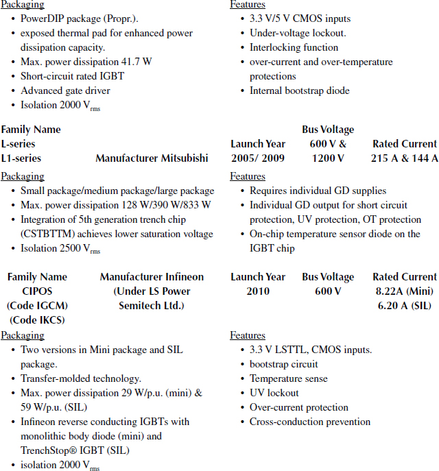
Each major power semiconductor manufacturer came with its own solution for power modules since the first IPM products in late 1990s [7]. Table 10.1 provides some examples of conventional IPM devices. The quoted numerical data is just an example able to sustain the theory developed within this chapter and there is no intention to compare performance. Many other manufacturers like Cyntec and Sanyo (now within ON Semiconductor) may have not been included herein simply for space reasons.
TABLE 10.1
Examples of 3-Phase IPM Technologies in Arbitrary Order [2,8,9,10]

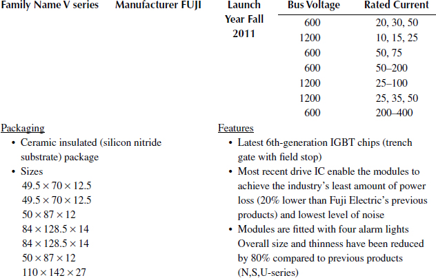
A new generation of high power devices has been launched in late 2011 and they can be seen as an important leap forward for their expanded power in the range of 100 s Amp (Table 10.2). We are seeing this as a very important technological advance since it pushes the envelope of this technology across the entire low-voltage IGBT product range (low voltage in the sense of power systems that is below 1500 V).
TABLE 10.2
Latest High Power IPM Product Announcements [11]
The advent of IPM devices has opened some new R&D opportunities for the system designer which does not have to worry about the optimization of the low-level design for the gate driver and protection. The power electronics designer can therefore focus on performance achievements at system or power circuitry level. New multiswitch topologies can hence be created and some of them are presented in Chapter 18.
These IPM devices are integrating semiconductor devices along with their cooling structures, with very limited or without passive components. The power electronics designer benefits now from all these topologies that do not contain passive components. It generally does worth trading the integration of multiple semiconductors against the reduction of the passive components count in power electronics equipment. This is the core idea of the advanced research presented in Chapter 18. They all can be subscribed to a design trend for all-semiconductor power conversion solutions able to increase the reliability, and maintainability.
Designing a power circuit with IPM devices includes setting up the following low power external components [12]:
• Bootstrap power supply should supply the high-side gate circuit without dropping below the UVLO threshold (typically around 11 V);
• Bypassing the local power supply for the HVIC;
• Certain IPM devices come with internal thermistor for temperature monitoring and over-temperature protection;
• Certain IPM devices come with an option for external resistor to sense current, and others have the sensing circuitry already internally.
Among all these tasks, the design decision for the floating (high-side) power supply is the most open to debate. The conventional supply of each channel is done with a topology called bootstrap power supply (Figure 10.5). This is based on charging the supply (bootstrap) capacitor for the high-side circuitry during the conduction time of the low-side IGBT from the low voltage power supply used for the circuitry related to the low-side device. After turning-off the low-side IGBT, the gate driver (protection and control) of the top-side IGBT is supplied from the energy stored within the bootstrap capacitor.
The bootstrap capacitor is usually a ceramic MLCC capacitor able to behave well in high frequency while storing the required energy. While a combination of ceramic and electrolytic capacitors was traditionally of choice, the recent availability of ceramic capacitors with large capacitance value suggests the setup of the bootstrap capacitor with a single ceramic capacitor. This is usually selected with a value of 1 to 47 μF, and rated at 25 V.
The bootstrap diode needs to withstand 1.5 times the bus voltage, and this becomes usually a requirement for a 1000 V diode when used along a conventional 600 V IPM. Moreover, it has to be a fast recovery diode, 50 ns or better, at 1–2 A.
Finally, inserting a damping resistor (Rboot = 1 to 5 ohms) in series with the bootstrap diode is an effective way to eliminate some important problems like:
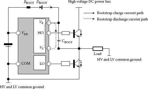
FIGURE 10.5 Principle of bootstrap power supply.
TABLE 10.3
High-Side Power Supply Requirements
Topology |
Figure |
Comments about ton/toff |
Bootstrap Possible? |
Simple parallel |
Normal PWM |
Yes |
|
Interleaved |
Normal PWM |
Yes |
|
Parallel assembly diode/CSI |
1/3 cycle |
Maybe w/special design |
|
Multilevel |
Normal PWM |
Yes |
|
Conventional matrix w/CSI |
Large toff |
No |
|
Direct converter w/VSI |
Normal PWM |
Yes |
|
Novel topology |
Large toff |
No |
• EMI noise due to possible reverse recovery charge of the bootstrap diode.
• Overcharge of the bootstrap capacitor by a negative spike on the VS voltage, spike induced by the stray inductance on the negative line.
Some other minor precautions are required at the design of the HVIC and at the start-up of the entire operation.
The issue with this cost-effective bootstrap power supply comes when using the IPM in a nonconventional way. For instance, the special case of using IPMs within the special topologies is proposed later on in Chapter 18. These cannot benefit from the low-side conduction due to the large interval of pause in operation.
Table 10.3 reviews the power supply requirements in this respect.
A possible solution to this matter consists of the independent supply of each gate driver. This is done in industrial systems with special flyback configurations. In the case of topologies built with multiple modules, such option is not feasible and also departs from the goals of modularization and reduction of passive components. The possible elimination of passive components and a design close to the all-semiconductor approach improves reliability and reduces loss [13].
A switch-mode unregulated dc/dc converter can be used instead and this is an ideal circuit substitute for the bootstrap diode (Figure 10.6). For instance, the RECOM dc/dc switch-mode converter comes in a small SIP4 package, works without a requirement for external components and without heat-sink, while offering unregulated 15 V/15 V conversion, 1000 V isolation, 2 W output (133 mA) at an efficiency of 80–85%. It can accommodate a capacitive load of up to 680 μF, more than enough for a large majority of gate driver applications. Multiple other manufacturer options are available.
For a numeric design, consider a maximum gate current request of 4.5 A for 500 ns, the minimum supply capacitor required to minimize the voltage drop at 1 V yields:
(10.1) |
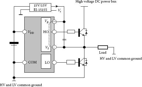
FIGURE 10.6 Using the unregulated 15/15 V power supply, with 1000 V isolation.
A ceramic capacitor MLCC of 10 μF at 25 V, in a surface mount 1206 package can be adopted for any IRF IRAMS. Alternatively 22 or 47 μF nominations are also available in ceramic surface mount technology.
The use of a dc/dc hybrid converter is obviously more expensive, but it solves a series of problems with bootstrap power supply and can provide for a great laboratory setup needed to develop new control algorithms for all the novel topologies proposed in Table 10.3.
10.3.2 CLAMPING THE REGENERATIVE ENERGY
The main use of IPM devices relates to AC loads and the designer should address the operation with an inductive load after the operation of the switches ceases for voluntary or involuntary reasons. This may be the case of a faulty condition when all the switches turn-off for the protection of the drive and the energy from the load needs a path to discharge. Otherwise damage to the power semiconductor devices can occur.
The most used method for de-energizing the load in such situations consists of a current path through diodes. Moreover, the intermediary DC bus capacitor of a back-to-back configuration may need sometimes a quicker discharge or voltage limitation through a brake resistor. Such brake or discharge resistor is connected across the DC capacitor with a 7th switch. While the back-to-back converter topology is inherently using the existing diodes within the two IGBT six-packs, any of the direct (matrix) converters proposed in Chapter 18 needs to use an additional dual diode bridge circuitry from input to output. Such additional clamp circuitry is mostly needed even if it is not shown in the main circuit topology drawing.
On the other hand, the conventional IPM devices are intended for low power applications, with currents below 50 A. In such case, the preferred protection is conventionally based on varistors as shown in Section 6.2.4. For all the other operation modes requiring a regenerative discharge of the load, these converters are four-quadrant and they can easily manage the energy flow from the load to the grid.
1. Motto, E. 1998. Application specific intelligent power modules—A novel approach to system integration in low power drives. PCIM Conference.
2. Bhalerao, P. and Wiatr, R. 2008. New intelligent power module series. PCIM Europe, 2, pp. 21–22.
3. Motto, E.R. and Donlon, J. 2006. Speed shifting gate drive for intelligent power modules. IEEE APEC.
4. Neacsu, D.O., Nguyen, H.H. 2002. US Patent #6,459,324—Gate drive circuit with feedback-controlled active resistance.
5. Neacsu, D.O. 2001. Active gate drivers for motor drive applications. IEEE PESC2001, Vancouver, Canada, June.
6. Giacomini, D., Bianconi, E., Martino, L., Palma, M., 2000. A new fully integrated power module for three-phase servo motor driver applications. International Rectifier Application Paper.
7. Tolbert, L. 2012. Smart integrated power module. Project ID: APE046, 2012 U.S. DOE Hydrogen and Fuel Cells Program and Vehicle Technologies Program Annual Merit Review and Peer Evaluation Meeting.
8. Anon. 2008. IRAMS10UP60B-iMotion Series. Integrated power hybrid IC for appliance motor applications. International Rectifier’s Datasheet.
9. Anon. 2010. STGIPS10K60A—IGBT intelligent power module. ST Microelectronics’ Datasheet.
10. Lee, J.B., Lee, J.H., Cho, J., Chung, D.W., and Frank, W. 2010. AN-CIPOS mini-1-Technical Description, Infineon/LS PowerSemitech Application Note.
11. Shimizu, N., Karasawa, T., Takagiwa, K. 1012. New lineup of large-capacity “V-Series” intelligent power modules. Fuji Electr. Rev. 58(2) 65–69.
12. Schimel, P. 2011. A few useful tricks for modular inverter design. IEEE APEC special session SP-2.2.1.
13. Neacsu, D.O. 2010. Towards an all-semiconductor power converter solution for the appliance market. IEEE Industrial Electronics Conference IECON, Glendale, AZ, USA 2010.