
11.1 REDUCING SWITCHING LOSSES THROUGH RESONANCE VERSUS ADVANCED PWM DEVICES
It has been shown in the introduction that a switching operation is adopted in high-power converters in order to reduce losses and to improve efficiency. However, the operation of the power semiconductor devices is far from ideal and losses still occur. It has also been shown in Chapter 2 that these losses arise during ON-time and during transient events.
Losses during ON-time are called conduction losses and they depend entirely on the voltage drop across the switching device. Modern MOSFET devices feature very low Rds(on) [1]. For instance, the CoolMOS devices can switch up to 85 A at 600 V and benefit from an Rds(on) of 35–70 mΩ (see the topmost IXYS IXKK 85N60C), while the newest Q2-Class HiPerFET devices can switch up to 80 A at 500 V and benefit from an Rds(on) of about 60 mΩ. Other conventional high voltage MOSFETs have Rds(on) in the range of 150–200 mΩ. Versions of these technologies of MOSFETs can be switched up to 1200 V. Analogously, new technologies reduce the ON-state voltage drop across insular gate bipolar transistors (IGBTs) to the range of 2–3.5 V. Trench-gate IGBTs are recommended for low conduction loss with their collector–emitter voltage drop of 1.5–2.2 V (for instance, see Powerex CM200DU-12F for 200 A at 600 V) [2]. All these technology advancements are remarkable, and efforts will continue in the coming years on the same lines. Conduction loss, however, is technology-dependent and cannot be minimized by application topology. The only thing the designer can do is to estimate the weigh of the conduction versus switching loss within the application and select the proper power switch. If low conduction loss is more important for the application, devices with lower conduction loss should be selected. If, on the contrary, operation at a high switching frequency is required, devices with short transient times should be selected.
The second major category of losses is due to the transients of the voltage and current at turn-on and turn-off of the power semiconductor devices. When power devices change their conduction state, voltage and current have finite transitional slopes that superimpose for a short time, creating switching loss. The amount of switching loss at turn-on or turn-off of any switching device depends on both the technical characteristics of the power device and the application circuit. Here, there is room for improvement and for energy saving by the designer of the circuit. We dedicate this chapter, therefore, to understanding what energy savings are achievable with help from the circuit design engineer.
A complete analysis of the switching processes within power semiconductor devices has been presented in many books or papers. We limit this presentation to understanding the timing of a switching process. Figure 11.1 shows device behavior at turn-on. These waveforms have also been presented in Chapter 2 along with the definition of the most appropriate gate-driver design.
The semiconductor’s power loss is calculated with the product of drain-source (collector–emitter) voltage and source (emitter) current. This product is obviously large during the switching process. At turn-on, the current changes its state before the voltage change and the sequence of transitions is reversed at turn-off. Furthermore, the turn-off of the IGBT or bipolar power transistors is characterized with a tail current that increases the switching loss.
The minimization of the switching loss is possible by reducing the time interval when both voltage and current are not close to zero. Different gate-driver techniques account for a controlled slope of voltage and current transitions. There are however limits to this minimization. The transition of current cannot be too steep as it would produce large voltage spikes in all the circuit parasitic inductances. The voltage slope is generally limited within the semiconductor device technology and the resulting parasitic capacitances have finite values.
Observing Figures 11.1 and 11.2 brings into focus the timing of the current and voltage waveforms as another possible solution for loss minimization [3]. Obviously, the switching loss depends on the amount of time between the voltage and current transitions. If somehow, we could move the voltage transition before the current transition, as shown in Figure 11.1, the switching loss would approach zero. Analogously, moving the transition of current before the transition of the voltage minimizes loss in the turn-off process.
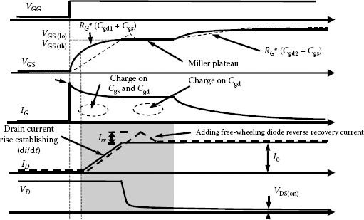
FIGURE 11.1 Generic turn-on waveforms for an IGBT/MOSFET power device.
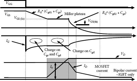
FIGURE 11.2 Generic turn-off waveforms for an IGBT/MOSFET power device.
Chapter 1 explained the role of power semiconductor devices in processing high power and the importance of maintaining simple circuit schematics. Changing the sequence of voltage and current slopes will definitely complicate the circuit schematic and this is the major trade-off a power circuit designer will face when selecting the proper topology for a power-conversion system. To keep the circuit schematics at a reasonable level of complexity, resonant circuits are used to change the sequence of voltage and current slopes. These can freely oscillate or they may require synchronization with the power-switching pattern. Such synchronization usually requires the introduction of more switches, and a pertinent analysis should be done to justify the energy lost in the newly added devices versus the switching-loss savings in the main power stage.
This chapter introduces the Reader to the philosophy of using resonant power converters in high-power conversion systems and provides several examples for circuits. Given the dynamic market for power semiconductor devices, the goal here is not to provide a comprehensive analysis of all possible switching devices, but to present the reasoning that will help a power electronics engineer to make the right topology selection decision.
11.2 DO WE STILL GET ADVANTAGES FROM RESONANT HIGH POWER CONVERTERS?
Let us start with a bit of history. The first widely used power semiconductor device was the silicon-controlled rectifier (SCR), also called thyristor. This device could be turned-on by a control signal and conduct current like a diode before the external circuit conditions turned it off. The use of this device in inverter type of applications required special turn-off circuits. Some of these turn-off circuits were built with resonant L–C networks.
The development of GTO (gate turn-off) devices for high-power conversion circuits simplified the inverter building. The GTO devices had a very large tail current at turn-off and efficiency optimization brought back the need for resonant circuits.
Later on, IGBTs became the main choice for power semiconductor devices. In 1982, RCA and General Electric virtually simultaneously announced the discovery of this device [4]. It seemed to be the perfect device for switching high power and, in the early 1990s, almost all production of power converters in the 10–100 kW range was based on IGBTs.
First generation IGBTs, however, continued to have large switching losses. Reducing switching loss in IGBTs was one of the most important subjects of R&D efforts in the early 1990s. Hundreds of papers or patent applications were written and, probably, every researcher in this field was, in one form or another, involved in researching new, resonant-power converters for high-power applications. These circuits were actually not entirely new, as they could be adapted from resonant converters built much earlier with SCR or GTO devices.
Two important research directions have emerged from these preoccupations [5]. The first addresses the invention and development of new, resonant-converter topologies. A possible classification of these solutions for inverter applications follows and more detail is provided in a further section.
Classification by the position of the resonant circuit:
• Resonant circuit in the DC bus allows a simplified six-switch converter topology
• Resonant circuit on each converter leg (pole voltage)
• Resonant circuit around each semiconductor switch
• Resonant circuit in the output
Classification by the signal used in reducing losses:
• Zero voltage switching: the voltage is kept at zero during the switching process
• Zero current switching the current is null during the change of conduction state
Classification based on the complexity of the resonant circuit:
• Free-running, continuous, resonant operation
• Synchronized resonant swing before the desired switching of the main device
This R&D direction has also addressed the mathematics of calculating the resonant-circuit operation, the resonant-component selection, and the possible variations in the values of the resonant circuit’s passive components.
The second research direction addresses the system implications of resonant circuits and efficiency improvements. The following topics have been analyzed:
• Understanding the reduction in switching loss at the power-switch level by comparison with a hard-switched device.
• Evaluating the additional loss introduced by the resonant circuit and the switching circuit managing the release of the resonant swing.
• Understanding the additional stress in the power semiconductor devices and addressing the trade-offs between efficiency improvement and weak switch utilization.
• Implementation of the digital controller with the most appropriate switching pattern timing in the power stage and for the resonant circuit.
The major merit of this second direction in R&D efforts was to acknowledge the potential drawbacks of using resonant converters and to establish a proper comparison of losses at the system level rather than at the switch level. Some researchers defend the use of resonant converters by claiming that the spread of losses over several devices and components would help the cooling system. This is entirely true and moves the use of resonant converters into a much general class of applications.
In the early 1990s, power converters with soft-switching operations were reported to save up to 10% of the switching loss. More recent implementation solutions are claiming a reduction in power loss of between 2% and 5%. Attention should be paid to how these savings are estimated.
Throughout the 1990s, semiconductor technology evolved continuously and the latest IGBT generation features excellent switching times and substantial loss reduction. The IGBTs’ relatively long turn-off time—they required as much as 2 ms to turn off—was a major shortcoming of the first generation. Technology improvements made possible turn-off in less than 200 ns. The latest generations of IGBTs especially designed for switched-mode power supplies and UPS applications can turn off in less than 100 ns. This reduces loss and makes IGBTs compatible to or better than MOSFETs in high-voltage applications that operate at more than 100 kHz. The maximum attainable switching frequency has also changed over the years from 10 kHz to more than 100 kHz [6,7].
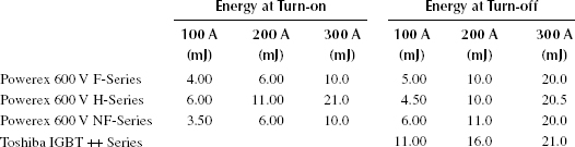
To better assess the developments in IGBT technology, let us consider data from Tables 11.1 and 11.2. These are datasheet extracts. We acknowledge that measurement and reporting conditions vary from manufacturer to manufacturer, and we show this data only to assess the level of expected switching loss in hard switched converters. The data are in no way a direct performance comparison. It is important to note that such levels of switching loss make it difficult to further improve resonant circuits.
TABLE 11.1
Switching Loss Comparison for 100 A IGBT Devices (Energy Per Pulse)
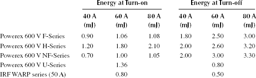
TABLE 11.2
Switching loss comparison for 400 A IGBT devices (energy per pulse)
The advent of technology in the power semiconductor industry and the required complexity in the control circuit of resonant converters minimized the application of this technique within the large-scale production of power converters in the range of 10–100 kW. Almost all manufacturers of power converters took a conservative approach in maintaining production of hard-switched converters and targeting efficiency improvement by reducing parasitics, timely commissioning of new semiconductor devices, and working towards the most optimal gate-driver circuits.
However, there are many applications where resonant circuits are the best choice [5,8,9].
• Many high-voltage and high-power converters continue to use SCRs, GTOs, or older generation IGBTs that may benefit from resonant-circuit techniques.
• Power converters used in very high-temperature environments may benefit from a reduction of losses in the main switching devices or a slight transfer of losses in the resonant circuit.
• The use of very modern or advanced power semiconductors at the edge of their ratings. For instance, building power converters with the new CoolMOS or HyperFET devices allow switching at 600 V and 200 kHz of a current of 20–50 A. If increasing the switching frequency further provides any benefit to the application (size of magnetics, for instance), resonant switching is a good choice.
• Building power converters to fit extremely small spaces may require the use of resonant converters.
Let us consider the switching of power semiconductor devices under zero voltage or zero current and make this analysis independent of the circuit topology.
11.3 ZERO VOLTAGE TRANSITION OF IGBT DEVICES
11.3.1 POWER SEMICONDUCTOR DEVICES UNDER ZERO VOLTAGE SWITCHING
Switching loss can be reduced by bringing the voltage across the semiconductor device at zero before the turn-on process. The resonant circuit should be activated at switching instant only and this suggests the use of the term “quasi-resonant” for this class of converters.
It is important to understand the physics inside the power semiconductor devices switched at zero voltage in order to better assess the energy savings and possible failure associated with this operation mode.
Figures 11.1 and 11.2 emphasize the drain-source (emitter–collector) voltage trip during the Miller plateau of the gate voltage. The gate-drain capacitance provides a feedback path from drain to the gate that increases the equivalent charge needed for switching in the gate circuit. The total dynamic input capacitance results are greater than the sum of the static electrode capacitances. This effect, called the Miller effect, was first studied by John Miller for vacuum tubes. During the first voltage rise of the gate voltage, the gate-to-source capacitance gets charged, and during the flat portion (Miller plateau), the gate-to-drain capacitance gets charged. The total drive charge is typically higher for the Miller capacitance than for the gate-to-source capacitance. The width of the Miller plateau strongly depends on the amount of voltage seen on the drain (collector) of the power semiconductor device. Figure 11.3 shows the dependence of the gate voltage on drain current and voltage at turn-on. At the second voltage slope, both capacitances are charged as required by the switching of both voltage and current in the power stage.
During a zero-voltage transient, the Miller plateau disappears, as there is no voltage difference requiring additional charge into the gate-to-drain capacitance. This is important at the design of the gate circuit, as the overall charge is reduced and the stress in the gate driver is diminished.
Keeping in mind this behavior of the gate circuit, let us consider the selection of the proper power semiconductor device for a zero-voltage transition (ZVT). Usually, the switching performance is analyzed based on a combination of required gate charge and transconductance. Let us compare two devices with the theoretical characteristics shown in Figure 11.4. The first slope of the gate voltage is determined by the gate-source capacitance, which is larger for the second device. The second device has a higher transconductance and therefore requires less voltage on its gate for the given amount of collector current. This results in a faster device and in the interesting conclusion that the device with the smaller gate capacitance is not always the fastest.
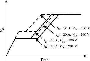
FIGURE 11.3 Gate voltage at turn-on for different current and voltage levels.
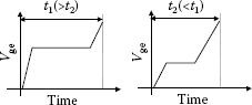
FIGURE 11.4 Different gate characteristics.
Considering the same power devices for a comparison of their operation under zero-voltage transient outlines the advantage of selecting devices with smaller gate capacitances, as the transconductance effect is reduced by the zero voltage present in the drain (collector).
Let us consider Figure 11.2 in relation to the turn-off of a power semiconductor device. The turn-off process can be seen as the reverse of the turn-on, except for the tail current characteristic of IGBT devices and not present in the switching of the power MOSFETs. The existence of the tail current can be explained with the pseudo-Darlington connection of two transistors in the IGBT model (Figure 11.5). The base of the second (the PNP) bipolar transistor is not accessible for additional control and its turn-off is totally dependent on the internal physics of the device. As the MOSFET channel stops conducting, electron current ceases, and the IGBT current drops rapidly to the level of the whole recombination current at the inception of the tail. The lifetime of the minority carriers at this junction, therefore, slows down the overall transient time by introducing a time interval to remove the tail current. Traditional lifetime-killing techniques and/an n1 buffer layer to collect the minority charges at turn-off are commonly used to speed-up this recombination process. Because these techniques reduce the gain of the PNP transistor, they also increase the voltage drop on the IGBT device. Moreover, this solution of lifetime killing to collect minority charges at turn-off may increase turn-on losses due to a quasi-saturation condition at turn-on. The existence of the tail current limits the use of a zero-voltage transient at the turn-off of IGBT devices [5,10,11].
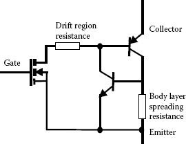
FIGURE 11.5 Equivalent circuit for an IGBT device.
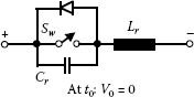
FIGURE 11.6 Quasi-resonant circuit for ZVT, with initial zero voltage on capacitor.
The operation of the quasi-resonant power converters providing ZVT can be defined on the basis of the initial conditions in the resonant circuits or the circuit topology. A first solution is shown in Figure 11.6, where the resonant cycle starts with zero voltage across the resonant capacitor. After the switch turns-off, a resonant circuit is formed with a resonant capacitor Cr and inductor Lr. If the period of the resonant circuit is chosen such that the voltage across the switch is again zero when turn-on is desired, then switching loss is minimized.
An alternative to this solution is shown in Figure 11.7. The Cr is now connected to an external potential Vref constant during the resonant cycle. The equivalent small-signal models of the circuits shown in Figures 11.6 and 11.7 are identical.
Let us take a very simple example to illustrate this principle [5].
Figure 11.8 shows a single-switch buck converter with commutation at zero voltage. Chapter 3 has already shown the reduction of three-phase converters to simple buck or boost power stages. Understanding this simple resonant circuit helps the development of complex three-phase resonant converters.
The operation of the power switch within this power converter follows the same control characteristics as the conventional buck converter and we can consider the load filter L–C as being ideal (Figure 11.9). Its equivalent effect is a constant DC load current denoted by IL.
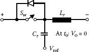
FIGURE 11.7 Quasi-resonant circuit for ZVT, with initial zero voltage on capacitor.
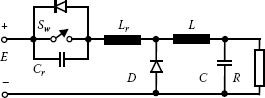
FIGURE 11.8 Quasi-resonant circuit for ZVT, with initial zero voltage on capacitor.
Let us start the analysis with the turn-off process. The voltage across is initially zero. The load current IL circulates through the resonant inductor Lr and the resonant capacitor Cr. This produces the linear increase of the voltage at the capacitor terminals.
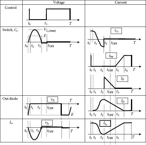
FIGURE 11.9 Voltage and current waveforms.
(11.1) |
The voltage across the resonant inductor lr is maintained null due to the constant load current. This implies a linear variation of the voltage across the buck diode D.
(11.2) |
At moment t1, the diode D has a positive bias and turns-on.
(11.3) |
The resonant circuit can be characterized with a resonant frequency fr and a characteristic impedance Zr.
(11.4) |
(11.5) |
These are also related by the following equations:
(11.6) |
(11.7) |
Equation 11.3 can be written in dependence with these variables.
(11.8) |
If the characteristic impedance Zr is chosen very large, the time interval t1 can be considered very small or at least much smaller than the switching period of the buck converter.
During the following time interval, the diode D conducts the load current and the switch Sw remains in the off state. The input voltage E is seen across the resonant circuit Lr–Cr and the voltage across the resonant capacitor Cr is given by:
(11.9) |
vcr(t)=E+Zr⋅IL⋅ sin [ωr⋅(t−t1)] |
(11.10) |
where the initial value of the current through the resonant inductor has also been considered.
The sinusoidal voltage across the resonant capacitor Cr reaches a peak voltage vCr(max) and then decreases to zero.
(11.11) |
The moment of time when voltage reaches zero yields:
t2=t1+1ωr⋅[π + arcsin (EZr⋅IL)] |
(11.12) |
The current through the resonant circuit in this moment is given by:
iCr(t2)=iLr(t2)=−IL⋅√[1−[EZr⋅IL]2] |
(11.13) |
The current through the output diode at t2 yields:
iD(t2)=IL+IL⋅√[1−[EZr⋅IL]2] |
(11.14) |
When the resonant voltage prepares for the negative swing, the anti-parallel diode turns-on. This ensures the circulation of the current through the inductance Lr until the energy is discharged. During this interval, the voltage across the Lr is maintained constant. The current passing through Lr and the anti-parallel follows a linear variation:
iDSw(t)=iLr(t)=[−IL√[1−[EZr⋅IL]2]]+EL⋅(t−t2) |
(11.15) |
The current through the output diode D yields:
iD(t)=IL⋅[1+√[1−[EZr⋅IL]2]]+ELr⋅(t−t2) |
(11.16) |
The moment of time t3 when the current through the resonant inductor and the anti-parallel diode vanishes yields from Equation 11.14:
t3=t2+1ωr⋅Zr⋅ILE⋅√[1−[EZr⋅IL]2] |
(11.17) |
When the switch Sw turns-on, the current circulates through Sw, the resonant inductor Lr and the output diode. Because the output diode is still in the ON state, the voltage across the resonant inductor equals the input voltage E. The current will continue the linear variation from zero to the load current IL determining the same variation of the current through Dsw, Lr, and output diode D.
iDSw(t)=iLr(t)=[−IL√[1−[EZr⋅IL]2]]+ELr⋅(t−t2) |
(11.18) |
iD(t)=IL⋅[1+√[1−[EZr⋅IL]2]]+ELr⋅(t−t2) |
(11.19) |
The output diode current will eventually vanish at a moment of time t4 that is given by:
(11.20) |
where the results from Equations 11.16 and 11.17 are considered.
Finally, after the moment t4, the switch is the only device carrying current towards the load through the resonant inductor Lr. The state of this switch can be changed at any time and the entire operation cycle is repeated.
It is important to note that the moments t2 and t4 are very important, as they limit the possible variation of the ON and OFF time intervals within the controller operation. Their values are given by Equations 11.12 and 11.20 and these are dependent on both the passive components Lr and Cr as well as on the load current and supply voltage. The load current is the only variable parameter during the operation of the power stage.
The proper operation of the resonant circuit should respect the following constraint:
(11.21) |
It can be seen that the ZVT can be obtained for certain current levels and that light loads do not concur to reduction of the switching loss. One can also notice that the switching loss for a light load is anyhow reduced.
This converter can control the output voltage only by changing the period of the entire cycle that modifies the value of T or the moment when the switch is turned off. The duration of the OFF state is dictated by the circuit conditions. The averaged output voltage can be calculated by:
(11.22) |
This, unfortunately, is dependent on both the load current and the input voltage and can be controlled only by the cycle period. However, this analysis illustrates the operation of a simple resonant circuit and does not have as its objective the design of a complete power converter.
The voltage across the power switch is increased to Cr(max) from the input voltage E. Depending on the current level, this can be up to twice as much as the input voltage. This obviously means to overrate the power switch. When using IGBTs, there is not much difference in the conduction losses in devices of 600 and 1200 V. However, using MOSFETs implies a substantial difference between Rds(on) of devices rated at 250, 500, and 600 or 1000 V, as they are the result of different technologies. The ratio of Rds(on) can be twice as much. Moreover, there is more current passing through the switch and the conduction loss is larger. A fair loss comparison should definitely include both the optimization of the switching loss and the change in the conduction loss.
Many power conversion applications require a power transfer from a low-voltage source to a high-voltage load through a step-up conversion [3]. Figure 11.10 shows a possible resonant circuit for this condition. The input inductance L can be modeled with a current source.
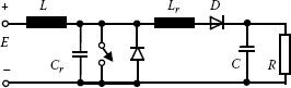
FIGURE 11.10 Step-up power converter.
Let us assume that the general operation of this boost converter is not modified by the presence of the resonant circuit, and let us start the analysis at the moment when the switch is turned-off. At that moment, the current through the Lr and the voltage across the Cr are zero. The output diode is also in the OFF state. The quasi-constant input current is linearly charging the Cr.
(11.23) |
(11.24) |
At the time t1, the voltage across the capacitor Cr reaches the output voltage V0 and the voltage across the output diode reverses its polarity. The time interval t1 can be calculated with:
(11.25) |
where the previous notations for ωr and Zr are considered.
At the moment t1, the diode turns on and the switch Sw maintains its OFF state. The input current is now shared between the resonant capacitor Cr and the output branch of Lr and diode D. The inductance Lr and the capacitor Cr form a resonant circuit supplied by the load equivalent voltage V0. This resonant circuit starts with the voltage across the capacitor equaling the load voltage.
(11.26) |
The voltage across the resonant capacitor increases from V0 to a maximum value and then decreases to zero.
(11.27) |
At moment t2, this voltage reaches zero.
(11.28) |
The resonant swing of the voltage reaches zero only if Zr*IL > V0. The current through the Cr is given by:
(11.29) |
and it has the final value
(11.30) |
Analogously, the resonant current through the Lr and output diode is given by:
(11.31) |
After moment t2, the resonant circuit has the tendency to swing the voltage across capacitor to negative values, but the anti-parallel diode turns-on and clamps this voltage. The Lr has a constant voltage across its terminals and the current through this inductance varies linearly from its initial value at t2.
(11.32) |
The current through the anti-parallel diode is given by:
(11.33) |
The moment t3 when this current vanishes is determined as:
(11.34) |
Unfortunately, this time interval depends on both the input current and the output voltage and it cannot be influenced by control.
The power switch should be controlled for the ON state at any moment during the time interval (t2, t3), before the anti-parallel diode would turn-off. In this way, the switch turns-on after the resonant current reverses its direction at t3. The linear discharge of the resonant current through the output Lr continues until t4.
(11.35) |
The switch stays in the ON state for the rest of the switching cycle and the load diode remains in the OFF state. The entire operation can be understood with the waveforms showed in Figure 11.11.
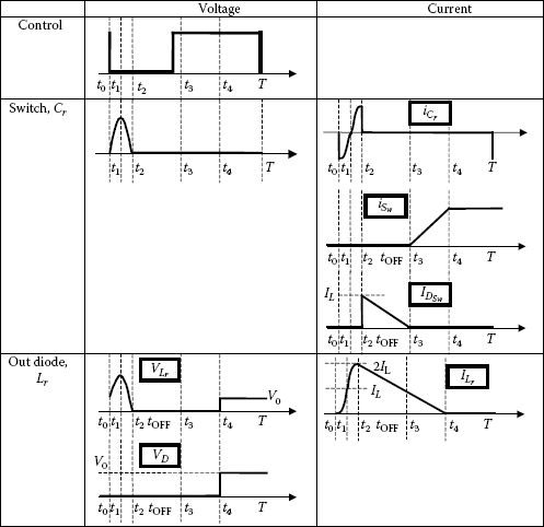
FIGURE 11.11 Voltage and current waveforms.
11.3.4 BI-DIRECTIONAL POWER TRANSFER
Many applications require a bi-directional circulation of the load current and the previous power stage is enhanced by the use of a dual module of MOSFET devices. To derive the resonant operation of such a two-switch converter, first let us note that the switch and the resonant inductor are in series, and their sequence can be changed without altering the operation of the converter (Figure 11.12). Replacing the buck diode with an assembly of switch, diode, and resonant capacitors leads to the sequence shown in Figure 11.13. The output filter does not have any effect on the resonant operation in the power stage and only a constraint of a constant load has been considered (Figure 11.14). The same operation will occur in a power stage without filter but with a constant load.
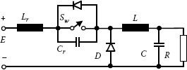
FIGURE 11.12 Another form of circuit from Figure 11.8.
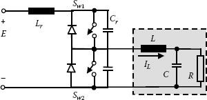
FIGURE 11.13 Power stage with dual module.
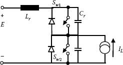
FIGURE 11.14 Equivalent model for the single leg converter of Figure 11.13.
Understanding the resonant operation of this converter implies analyzing separately the step-up and step-down power transfer from the “load” to the “input”. This can be achieved by considering the Sw2 as the power-commuting device and the diode D1 as the freewheeling diode for the step-up conversion from load, and Sw1 as the power commuting device and the diode D2 as the freewheeling diode for the step-down conversion. The same intermediate states occur for a negative load current.
Let us consider now the switch Sw1 in conduction and the current getting out of converter and circulating towards the load. When Sw1 is turned-off, both switches are in the OFF state and the parallel capacitors are charging from the load current. The high side capacitor that was initially discharged increases its voltage. The low-side resonant capacitor charged at the bus voltage, is now discharged with the load current. The pole voltage decreases according to the resonant circuit. The resonant swing of the voltage reaches zero before commanding the turn-on of the switch Sw2 if the initial value of the load current is large enough. If there is not enough energy in the load current, the switch Sw2 will be commanded when there is still voltage across it and it will turn on with switching loss (Figure 11.15).
Of most interest to us is the extension to the three-phase conversion systems. Figure 11.16 builds upon the theory developed in Chapter 3 and illustrates the principle of resonant circuitry applied to a three-phase conversion system. It is interesting to note that the resonant circuits shown in figure somehow occur naturally from the building of the power stage. The output capacitances (Coss) of the power MOSFETs or IGBTs and the bus-bar parasitic inductances represent a good starting point for constructing this resonant circuit.
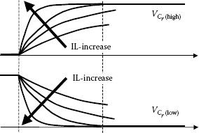
FIGURE 11.15 Resonant capacitors voltage.
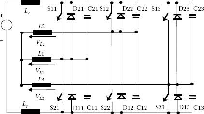
FIGURE 11.16 Three-phase system with resonant circuits.
One can notice the equivalence between this presentation of the Zero Voltage Transition (ZVT) methods and the resonant snubbers shown in Chapter 6, Section 6.2.5.5.
11.4 ZERO CURRENT TRANSITION OF IGBT DEVICES
11.4.1 POWER SEMICONDUCTOR DEVICES UNDER ZERO CURRENT SWITCHING
Let us re-analyze the switching of the power devices shown in Figures 11.1 and 11.2 with the condition of zero current in the drain circuit [1,12]. The first slope of the gate voltage ends faster due to the reduced Miller threshold at zero current. This is also explained in Figure 11.3. However, the Miller plateau is still dependent on the voltage from the drain-source (collector–emitter) circuit. After the voltage swings towards zero within a turn-on process, the current may be allowed to increase slowly to the actual value of the load current through a series inductance (Figure 11.17).
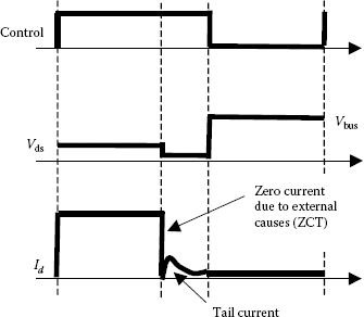
FIGURE 11.17 Turn-off characteristics with Zero Current Transition (ZCT).
The zero current switching at turn-off is ensured with an external circuit that cancels any drain current before the actual turn-off command. Excess charges thus get trapped within the power semiconductor device and they start decaying through internal recombination. The drain-source voltage has a fast rise after the turn-off command. This voltage is supported within the reverse-biased p-base drift region junction (Figure 11.5).
After the supply voltage has reached the drain-source (collector–emitter) circuit, the remaining process is a recombination that characterizes the tail current. This results in a turn-off current bump in the drain (collector) circuit. The excess carrier in the drift region can be swept away into the MOSFET channel in parallel with the recombination process if the gate voltage is still applied to maintain the inversion layer and the MOSFET channel. It is important to maintain the control voltage in the gate circuit, before all carriers are swept out through the MOSFET channel, in order to reduce the current tail and the current bump in the power circuit. This reduces switching loss accordingly. This brief analysis outlines the benefits of zero current transition (ZCT) in turn-off switching.
The ZCT class of resonant power converters is characterized by placing an inductor in series with the power switch and counting on a zero current at turnoff. Figure 11.18 shows a simplified circuit based on an additional voltage potential Vref and Figure 11.19 presents a solution without any other voltage source. This resonant circuit reduces losses at the turn-off of the power switch. Achieving zero current through the switch at turn-off is possible with a sinusoidal variation of the current through the resonant inductor Lr. Unfortunately, this swing of the current reaches a peak value of twice the load current and this large current passes through the power switch during the ON state. The rating of the switch should be increased and the conduction losses will increase accordingly.
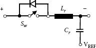
FIGURE 11.18 Quasi-resonant circuit for ZCT.
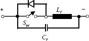
FIGURE 11.19 Quasi-resonant circuit for ZCT.
This resonant circuit reduces losses at the turn-off of the power switch. Achieving zero current through the switch at turn-off is possible with a sinusoidal variation of the current through the resonant inductor Lr. Unfortunately, this swing of the current reaches a peak value of two times the load current and this large current passes through the power switch during the on state. The rating of the switch should be increased and the conduction losses will increase accordingly.
Let us explain the operation of a resonant circuit for ZCT within a buck converter. The simplified circuit diagram is shown in Figure 11.20.
The operation of the buck converter should not change from the conventional power converter and the load current is assumed constant during the resonant cycle in Figure 11.21. Let us start this analysis with a zero current through the Lr and a zero voltage across the Cr, the load current being sustained by the output diode D.
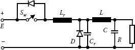
FIGURE 11.20 Quasi-resonant circuit for ZCT.
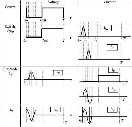
FIGURE 11.21 Voltage and current waveforms.
At t0, the switch is turned on and current starts to circulate through the Lr and the power switch with a linear variation.
(11.36) |
(11.37) |
The current through the output diode D is given by the difference between the load current and the current through the resonant inductor:
(11.38) |
At the moment of time t1, the current through the output diode reaches zero and the diode turns-off. Using Equation 11.7 yields:
(11.39) |
After t1, the load current passes through the power switch and the Lr. The Cr is no longer clamped at zero voltage and it can produce an additional current through the switch and the Lr. This capacitor starts to charge from zero voltage. The current through the Lr is now calculated for the resonant circuit Lr–Cr with initial zero voltage on the capacitor:
(11.40) |
(11.41) |
This current has a sinusoidal variation from the initial value equaling the load current to a maximum value and it is decreasing later to zero. The moment when the current vanishes yields:
(11.42) |
The voltage across the capacitor has a harmonic variation during the resonant cycle.
(11.43) |
The maximum voltage across the Cr is calculated with:
(11.44) |
It is important to calculate the amount of energy required by the resonant circuit in order to extend its swing to zero. This happens when the current in Equation 11.41 can reach zero and it yields:
(11.45) |
It can be seen that this solution does not work for large load currents. The maximum current through the power switch and resonant inductor is calculated as:
(11.46) |
This current can be more than two times the load current. The conduction loss within the switch is definitely increased by this additional current circulation.
After t2, the switch turns-off at zero current and both the power switch and the output diode are in the off state. The Cr takes over the entire load current and this produces the capacitor discharge.
(11.47) |
The linear variation of the voltage can be expressed as:
(11.48) |
The output diode turns-on at t3 when this voltage equals zero.
(11.49) |
After the output diode turns-on, the load current is circulated through this diode while there is no current circulation through the power switch and the Lr. After this moment t3, the power switch can be turned on at any time and the entire cycle is repeated.
Because the main power semiconductor switch turns-off according to the resonant cycle, the output voltage does not depend on the duty cycle of the control signal but on the resonant period.
(11.50) |
The current through the power switch is several times larger than the load current and this should be rated for larger currents. Further, the conduction loss is increased with this current circulation and this trade-off should be considered at the design of the power stage.
The principle of ZCT can also be applied to step-up converters. It is assumed that the operation of the resonant circuit does not affect the main function and operation of the original step-up converter. The only modifications are the presence of the series’ resonant inductor Lr and the parallel resonant capacitor Cr.
Let us start the analysis with the turn-on event (Figure 11.22). In the beginning, both the power switch and the output diode are in conduction and the voltage across the Cr is kept equal to the load voltage (Figure 11.23). The input current is split between the Lr and the load current. The current through the Lr inductance has a linear variation:
(11.51) |
FIGURE 11.22 Step-up converter with ZCT.
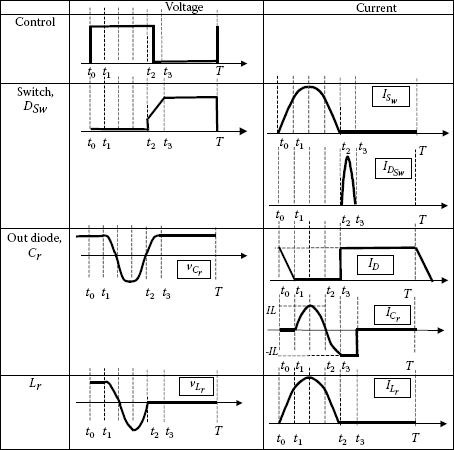
FIGURE 11.23 Voltage and current waveforms.
(11.52) |
The load current equals:
(11.53) |
and reaches zero at t1.
(11.54) |
After t1, the parallel resonant circuit Lr–Cr remains in the circuit and the Lr current is the result of the differential equation:
(11.55) |
with the following solution:
(11.56) |
The voltage across the parallel resonant circuit varies based on:
(11.57) |
The current through the Lr increases from the initial value to a maximum value and decreases to zero at the moment of time t2.
(11.58) |
This current also turns-off the switch under a ZCT. The resonant voltage at this moment reaches:
(11.59) |
After t2, the switch is in the OFF state and the resonant current continues through the anti-parallel diode. After the entire negative cycle of the current, the anti-parallel diode turns-off when current reaches zero again.
(11.60) |
The voltage across the capacitor Cr and inductance Lr moves to a level given by the following:
(11.61) |
The next switching of the main power device should occur after this time moment in order to be ready for another conduction interval.
The operation of this very simple resonant circuit determines an output voltage depending on the input voltage through a relationship with the resonant period as parameter. More complex circuits should be developed to ensure full control of the duty cycle and output voltage.
11.5 POSSIBLE TOPOLOGIES OF QUASI-RESONANT CONVERTERS
All the circuits presented and analyzed in the previous sections allow for low switching loss due to the zero voltage turn-on. Unfortunately, they represent a very simple solution without too many control features. Constraints in reduction of the switching harmonics push for precise ON and OFF time control. This implies use of more evolved circuit configurations. Several examples are shown in this section without a comprehensive analysis.
We can define a group of resonant three-phase power converters based on resonant circuits on each leg of the three-phase power converter. The operation of these resonant circuits is based on inverter pole measures. Several examples are shown in Figures 11.24 and 11.25. The first one represents a derivative of the circuit shown in Figure 11.13 and it is suitable for a zero voltage transient. The next evolutionary step takes place in the Auxiliary Resonant Commutated Pole Inverter (ARCPI, Figure 11.25). This has the ability to stop and release the resonant process at precise moments, controlling it by the use of the bi-directional switch. Pulse width modulation algorithms can therefore be improved and the harmonics in the load optimized. Different versions of these circuits have been proposed and their optimization focuses on the reduction of the ratings for the power semiconductors and passive components used in the filter.
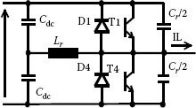
FIGURE 11.24 Conventional resonant pole inverter.
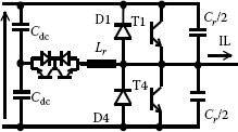
FIGURE 11.25 Auxiliary resonant commutated pole inverter.
Another class of converter moves the resonant circuit on the DC side in an effort to leave the main power stage unchanged from the hard-switched operation [10,11,12,13,14,15,16]. Advantages in packaging at module- or converter-level are therefore achieved. The resonant circuit on the DC bus produces a resonant swing of the voltage that is able to reduce the entire bus to zero. All power semiconductor devices in the main converter can, therefore, change their conduction state during this zero voltage interval.
The immediate drawback is the operation of the resonant cycle with pulse width modulations (PWMs), as there are limitations in the resolution of the PWM algorithm. The main six-switch power stage disperses the resonant train of pulses from the DC bus to the three phases according to a sinusoidal law. All power semiconductor devices should be rated for double the DC bus voltage in the circuit shown in Figure 11.26. However, this is the simplest solution for a resonant DC bus.
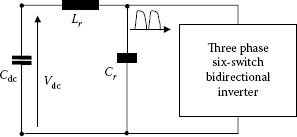
FIGURE 11.26 Simple resonant DC link three-phase inverter.
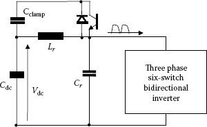
FIGURE 11.27 Resonant DC link three-phase inverter with a clamp circuit.
As this rating constraint is not easily achieved in a three-phase converter, a clamping circuit is introduced (Figure 11.27) to limit the voltage trip to high peaks by paralleling another capacitor that changes the period and impedance of the resonant circuit. The peak voltage is now limited to
(11.62) |
However, this solution does not allow any control of the pulse width and all pulses should be constructed with multiples of the resonant period. An alternative solution is shown in Figure 11.28 and consists in breaking the resonant cycle during the desired pulse width of the output voltage.
11.6 SPECIAL PWM FOR THREE-PHASE RESONANT CONVERTERS
The major issue with PWM control of resonant PWM three-phase converters consists in the minimum pulse-width required for allowing the resonant swing of either voltage or current waveforms. Several excellent PWM methods suitable for PWM control of resonant converters have been presented in Chapter 4, Section 5. Both the staircase PWM and the third harmonic injection PWM are good for the control of resonant power converters.
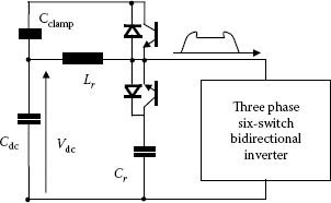
FIGURE 11.28 Fully controlled quasi-resonant DC link inverter.
A special class of three-phase resonant power converters is based on a continuous oscillation of the resonant Lr-Cr circuit. The PWM algorithm should therefore consider pulses with their width as multiples of the resonant period. Special optimization routines can be used to improve the PWM pattern. A good example in this direction has been already presented in Chapter 3, Section 7.3 as a binary programmed PWM algorithm.
P11.1 |
Determine the requirements of both the power switch Sw and the diode D for the converter shown in Figure 11.8 and operated according to Figure 11.9. Use all equations from 11.1 to 11.20 for this calculation. |
P11.2 |
Determine the requirements of both the power switch Sw and the diode D for the converter shown in Figure 11.10 and operated according to Figure 11.11. Use all equations from 11.23 to 11.35 for this calculation. |
P11.3 |
Determine the requirements of both the power switch Sw and the diode D for the converter shown in Figure 11.20 and operated according to Figure 11.21. Use all equations from 11.36 to 11.50 for this calculation. |
P11.4 |
Determine the requirements of both the power switch Sw and the diode D for the converter shown in Figure 11.22 and operated according to Figure 11.23. Use all equations from 11.51 to 11.60 for this calculation. |
P11.5 |
Demonstrate Equation 11.62. |
1. Anon. 2002. What is the benefit of CoolMOS in phase shifted ZVS bridge topology? Infineon Application Note, January.
2. Anon. 2000. Using IGBT modules. Powerex Application Notes.
3. Mohan, N., Undeland, T., and Robbins, W. 2002. Power Electronics. 3rd edition. John Wiley and Sons, New York.
4. Wheatley, C.F., Jr. and Becke, H. 1982. U.S. Letters Patent No. 4,364,073: “Power MOSFET with an Anode Region”, RCA, December 14.
5. Bose, B.K. 1992. Power electronics—A technology review. Proc. IEEE, 80, 1303–1334.
6. Travis, B. 2000. IGBTs come of age in switchers—New high-speed IGBTs can beat MOSFETs in conversion efficiency and silicon area in switching supplies operating at 100 kHz and faster. EDN 27, 42–46.
7. Ambarian, C. 1997. WARP SpeedTM IGBTs—Fast enough to replace power MOSFETs in switching power supplies at over 100 kHz. IRF Application Note, IRF Technical Paper, 1–6.
8. Huth, S. and Winterheimer, S. 1993. The switching behavior of an IGBT in zero current switch mode. Fifth European Conference on Power Electronics and Applications, vol. 2, pp. 312–316, 13–16 September.
9. Vlatkovic, V., Borojevic, D., and Lee, F.C. 1994. Soft-transition three-phase PWM conversion technology. IEEE PESC Conference Record 1, Taipei, pp. 79–84.
10. Divan, D.M. 1986. The resonant DC link converter—A new concept in static power conversion. IEEE-IAS Annual Meeting Conference Record, pp. 648–656.
11. Divan, D.M. and Skibinski, S. 1987. Zero switching loss inverters for high power applications. IEEE-IAS Annual Meeting Conference Record, pp. 627–634.
12. Imbertson, P. and Mohan, N. 1993. Asymmetrical duty cycle permits zero switching loss in pwm circuits with no conduction penalty. IEEE Trans. Ind. Appl. 29, 212–125.
13. Divan, D.M., Venkataramakan, G., and De’Doncker, R.W.A.A. 1993. Design methodologies for soft switched inverters. IEEE Trans. Ind. Appl. 29, 126–135.
14. Dehmlow, K., Heumann, R., and Sommer, R. 1992. Resonant inverter systems for drive applications. EPE J 2, 225–232.
15. Alexa, D. 1995. Resonant circuit with constant voltage applied on the clamp capacitor for zero voltage switching at the power converters. Elec. Eng. 78, 169–174.
16. Trivedy, M., Shenai, K., and Larson, E. 1997. Critical evaluation of IGBT performance in zero current switching environment. IEEE Conference Record, pp. 989–993.