
12.1 SOLUTIONS FOR REDUCTION OF NUMBER OF COMPONENTS
Previous chapters have extensively analyzed the three-phase converter based on six power semiconductor switches. One of the major preoccupations for the use of this conventional topology within industrial products is related to cost reduction. It has been shown that the largest cost share corresponds to building the power stage.
Accordingly, one approach to cost reduction would rely on seeking new topologies with a reduced number of components. This is especially important for applications in the horsepower range up to several tens of kilowatts.
Different solutions have been reported in the literature during the last twenty years or so. An important research direction has been dedicated to new grid interfaces with power factor correction. Some of them, including the single-switch, three-phase AC/DC converter, were analyzed in Chapter 9.
Constraints of variable frequency and magnitude for AC motor-drive applications have limited the efforts for new power converters used for simplified three phase AC sources. All reported solutions combine advantages and disadvantages versus the conventional six-switch inverter and none of them have really captured the market. These new solutions different from the conventional six-switch converter must be understood and studied for their merits and for the opportunity they provide to open up new directions for further research. They can be grouped in two categories:
• New inverter topologies: with reduced component count.
• Direct converters: to employ a single-power stage without intermediate DC link capacitor to perform direct AC/AC conversion.
12.1.1 NEW INVERTER TOPOLOGIES
The most well-known topology with reduced component count is shown in Figure 12.1 [1,2,3,4,5,6,7,8,9,10,11,12]. It is based on two inverter legs while the third phase is taken from the DC capacitor mid-point. This topology has proven merit to be considered for industrial implementation. For this reason, a special part of this chapter is dedicated to its full analysis. Similar application to AC/DC conversion stages has been considered.
An interesting combination of this topology, with a single-phase front-end converter, enabled use of a six-pack module for implementation of the whole AC/DC/AC conversion (Figure 12.2) [13]. The drawback is in the larger value of the DC capacitor bank. The two conversion stages (AC/DC and DC/AC) are controlled independently of each other and the additional control module manages the DC voltage within two threshold levels. A quick comparison with conventional topologies outlines the larger DC voltage on the bus. This aspect will be detailed in Sections 12.2 and 12.3.

FIGURE 12.1 Topology for a B4 inverter.

FIGURE 12.2 Reduced component count AC/DC/AC converter.
A completely different approach to reducing the number of components in the AC/DC/AC power electronic conversion supports a unidirectional load current (Figure 12.3a) [14,15,16,17]. If the load is a three-phase AC machine, it can be proven that this DC component does not affect the torque production but only increases the machine losses. Each leg is reduced to a DC/DC converter with a variable reference, as shown in Figure 12.3b.
These waveforms can be characterized mathematically by
i1d=Im⋅[u(ωt)−u(ωt−120)]⋅ sin ωt+Im.[u(ωt−120)−u(ωt−240)]⋅ sin (ωt−60) |
(12.1) |
(12.2) |
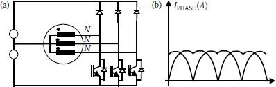
FIGURE 12.3 New DC/AC topology with unidirectional currents.
(12.3) |
One can verify that the difference between two reference currents is a purely sinusoidal wave. For instance: i1−2d = Im sinφt. It is very important to note that this set of phase currents produces a rotating magnetic field in the machine. In order to demonstrate this, let us first apply the vectorial transform (5.1) to the current waveforms shown in Figure 12.3b. This yields
(12.4) |
where
(12.5) |
After some calculation:
(12.6) |
The set of currents from Figure 12.3b generates a rotating magnetic field with constant angular speed and magnitude. A set of currents will be induced in the short circuited rotor and this will generate another magnetic field. The interaction between the stator and rotor magnetic fields produces a constant electromagnetic torque. The special shape of currents operates the induction machine under unstable conditions and the whole theory of induction machine dynamic model is not applicable here. Analysis should be performed on each interval separately. Stator and mutual equivalent inductances yield:
LsX=LsA+12⋅Ms(A,C)=Ls+12⋅MsLsY=LsC−12⋅Ms(A,C)=Ls−12⋅MsMs(X,Y)=√32⋅Ms(A,C)=√32⋅Ms |
(12.7) |
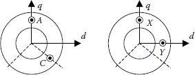
FIGURE 12.4 Transformation of (A,C) to (X,Y) system to prove the operation of the IM drive with the proposed currents.
where LsA = LsB = LsC = Ls and Ms(A,C) = Ms. The resulting voltage equations are similar to traditional dynamic equations for machine modeling except for the values of these inductances. The waveforms of the rotor currents are identical with those carried out for the same drive fed by sinusoidal currents with Im/√3.
A physical explanation of the machine operation is shown in Figure 12.4. Let us consider the time interval with a current passing through the wirings A and C of the stator while the current through the second phase B is zero. An equivalent bi-phase system can be derived for the first 2π/3 rad only if the flux in each wiring produced by the (X,Y) bi-phase system is the same as that produced by the (A,C) system.
Despite the interesting mathematical demonstration of the torque production, this three-phase power converter cannot be practically implemented in the form shown in Figure 10.3a. This is because the currents through the DC mid-point and DC capacitors flow in the same direction and have a tendency to discharge C1 and overcharge C2. In order to prevent this, a special DC/DC converter is proposed in [1,2] to regulate the voltage of the capacitors. This complicates the power stage design.
An alternative solution is proposed in Figure 12.5 [17]. One of the phases is built with a reversed direction and a different number of turns. This solves the problems in the DC bus if that phase current is double the value of each of the other two currents.
Unfortunately, this implies a specially built electrical machine, as shown in Figure 12.5.
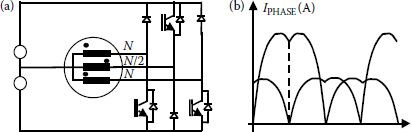
FIGURE 12.5 Implementation of the idea from Figure 12. 3.
Using the proposed converter and waveform solution increases losses in the induction machine. A simplified loss estimation is shown here.
• Stator copper losses
PCus=Rs⋅[12⋅π⋅2π∫0i2sdωt]⇒PCus=0.40⋅Rs⋅I2m=1.2067⋅Rs⋅[i2ds+i2qs] |
(12.8) |
When using the same induction machine (IM) as in a conventional case, an increase of 20.67% stator copper loss occurs.
• Rotor copper losses
When supplied with the proposed current waveforms, the rotor current’s sinusoidal waves and the rotor copper losses can be approximated as identical with the conventional case.
• Iron losses
A resistor equivalent to the stator iron losses can be included in the simplified IM equivalent model. This will be passed by a current equal with the difference between the stator current and the current through the magnetizing inductance. For a given torque, the stator losses can be somewhat reduced by a proper adjustment of the magnetic flux.
Even if these converter solutions are not very practical, they represent good conceptual advances in power converter technologies. Taking into account advanced mathematical theory may lead to new topologies in the future and understanding these advanced converters is a great start in researching emerging conversion approaches.
Given the cost and size of the passive filter components on the intermediary DC bus, solutions for direct conversion have been sought. First, a very simple but practical solution is presented in [18] and it represents the IGBT equivalent (Figure 12.6b) of a conventional SCR-based AC controller (Figure 12.6a) able to generate a three-phase system of voltages with a constant frequency and variable magnitude.
When high-side IGBTs are controlled, they connect the load to the grid. In contrast, when the low side IGBTs are turned-on, they short the load and separate it from the grid. A train of pulses is created and the root mean square value can be regulated appropriately.
These two topologies are recently revisited by employing Reverse Conducting IGBT devices (IGBT-RC), able to optimize the construction of the power stage.
In many motor-drive applications, both frequency and voltage need to be controlled and this can be achieved with different topologies of matrix converters. Given the importance of matrix converters within the power electronics landscape, Chapter 16 will present the conventional 9-switch matrix converters, and Chapter 18 will introduce special matrix converter topologies built of Voltage Source or Current Source 6-switch converters.
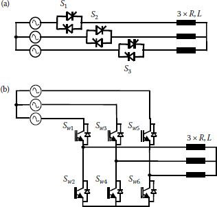
FIGURE 12.6 IGBT-based AC controller.
12.2.1 VECTORIAL ANALYSIS OF the B4 INVERTER
A new inverter topology with reduced count of components is built with two legs of the conventional inverter while the third phase is collected from the mid-point of the DC capacitor bank (Figure 12.1).
Let us first understand how this power converter operates. The third phase is taken from the mid-point of the capacitor bank and its pole voltage (M-Z) is always fixed at VDC/2. The phase voltages are constructed through a control on the other two inverter legs. The first consequence is the lack of zero states: there is no way the three pole voltages can be at the same potential during operation. This means that pulse width modulation (PWM) should be developed based on the remaining active vectors. A rule of operating a voltage source three-phase inverter says that we should always have one switch ON across each inverter leg.
This limits the number of the control states to four as shown in Table 12.1. A set of phase voltages can be generated by a combination of these states.
Phase voltages can be calculated from the pole voltages, as shown in Chapter 3. The appropriate equations are just adapted here to our inverter topology.
(12.9) |
TABLE 12.1
Possible Inverter States and Their Appropriate Voltages
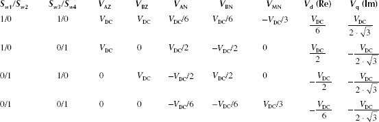
{va=vAZ−[vAZ+vBZ+vMZ]3vb=vBZ−[vAZ+vBZ+vMZ]3vc=vMZ−[vAZ+vBZ+vMZ]3 |
(12.10) |
The first attempts of using this topology have generated PWM with a conventional reference-triangle carrier based method. The reference waveforms have been considered sinusoidal with a 60° phase shift between each other. The pole voltages for the inverter legs can be written as:
(12.11) |
where fa and fb account for the high-frequency components due to switchings. If the load is heavily inductive or a motor drive, it is a good approximation to neglect these harmonics and to consider the effect of the waveforms in fundamental frequency only. It yields:
vNZ=VDC2+13⋅[V⋅ cos [ωt]+V⋅ cos (ωt−π3)]=VDC2+13⋅V⋅[2⋅cos[ωt−π6]⋅ cos (π6)] |
(12.12) |
(12.13) |
and
{va=[VDC2+V⋅ cos (ωt)]−[VDC2+1√3⋅V⋅ cos [ωt−π6]]vb=[VDC2+V⋅cos (ωt−π3)]−[VDC2+1√3⋅V⋅ cos [ωt−π6]]vc=[VDC2]−[VDC2+1√3⋅V⋅ cos [ωt−π6]] |
(12.14) |
{va=V⋅[cos (ωt)−1√3⋅cos (ωt)⋅√32−1√3 sin (ωt)⋅12]vb=V⋅[ cos (ωt−π3)−1√3⋅ cos [ωt−π6]]vc=−1√3⋅V⋅cos[ωt−π6] |
(12.15) |
In conclusion, this topology can be controlled by two sinusoidal references with 60° out of phase from each other in order to produce a symmetrical three-phase system. Moreover, these two references should be phase shifted with 30° from the desired first phase voltage (Figure 12.7).
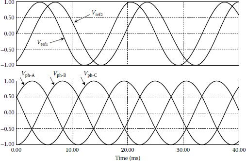
FIGURE 12.7 Phase information for the reference functions and desired fundamental phase voltages on the load (see Equations 12.11 and 12.12).
A similar control can be achieved by vectorial analysis. Let us apply transform relationship (5.1) to the phase voltages shown in Table 12.1. A vector in the complex plane will correspond to each operation mode. It is important to note that a different notation of the phase voltages in Figure 12.1 will produce other positions in the complex plane for the active vectors. The vectors shown in the complex plane of Figure 12.8 have magnitudes of VDC/√3 and, respectively, VDC/3.

FIGURE 12.8 Vectorial representation of the active vectors corresponding to the B4 inverter.
The generation of a symmetrical three-phase system assumes displacement of the tip of the voltage vector on a circular trajectory. The maximum radius of this circular locus is achieved when the trajectory is tangent to the polygon. It yields:
(12.17) |
Let us remember that the maximum voltage obtainable from a conventional six switches inverter was 1/√3⋅VDC (see Equation 5.31). The B4 inverter needs a double DC voltage in order to produce the same output phase voltage and this is a serious drawback of this topology. It produces increased voltage stress on the power semiconductor devices and electrical machine. The absolute value of the peak-to-peak ripple on the DC bus capacitor voltage is also increased. Finally, the third phase current circulates through the DC bank capacitor and this produces large variations of the voltage between the two capacitors. This can be corrected with large capacitors.
The two-leg inverter produces asymmetrical phase voltages as shown in Figure 12.9.
Since one leg circulates currents through the DC capacitor bank, asymmetries of the operation may introduce a third harmonic on the line-to-line voltages. The content of the third harmonic for the leg connected to the capacitor bank is twice as large as the third harmonic in the other two legs as they add up into the first one.

FIGURE 12.9 Typical phase voltages for the converter of Figure 12.1.
PWM generation takes into account the following constraints due to the asymmetries in operation:
• Decomposition on two adjacent vectors provides the average relationship.
• Because there is no true zero vector, two vectors with opposite directions are considered for equal time intervals to synthesize a zero-voltage state.
• There are always two possibilities for zero vector generation. It is preferred to use the “short” vectors for this since the “long” vectors produce larger voltage drop on the inductive load and larger ripple.
• In consequence, each vector generation is made with minimum three vectors: two short and one long.
• Several state sequences are possible.
The reduction of the number of switches determines cost reduction as well as conduction loss reduction in the power stage.
12.2.2 DEFINITION OF PWM ALGORITHMS FOR the B4 INVERTER
Two Vector PWM methods are herein investigated.
Method 1
The idea of vectorial decomposition on two neighboring vectors is considered for the two-leg inverter. If we consider the desired position of the voltage vector in between V2 and V3, the time intervals associated with each state are given by:
(12.18) |
{t2=Vs⌊V2⌋⋅Ts⋅cosϕt2=Vs⌊V2⌋⋅Ts⋅ cos ϕt13=Vs⌊V3⌋⋅Ts⋅sinϕ⇒t1=12⋅[Ts−Vs⌊V2⌋⋅Ts⋅cos ϕ−Vs⌊V3⌋⋅Ts⋅ sin ϕ]t0=2⋅t13=2⋅t1=Ts−t2−t13t3=Vs⌊V3⌋⋅Ts⋅ sinϕ+12⋅[Ts−Vs⌊V2⌋⋅Ts⋅ cosϕ−Vs⌊V3⌋⋅Ts⋅ sinϕ] |
(12.19) |
{t2=Vs⌊V2⌋⋅Ts⋅cosϕt1=12⋅[Ts−Vs⌊V2⌋⋅Ts⋅cos ϕ−Vs⌊V3⌋⋅Ts⋅ sin ϕ]t3=12⋅[Ts−Vs⌊V2⌋⋅Ts⋅ cosϕ−Vs⌊V3⌋⋅Ts⋅ sinϕ] |
(12.20) |
When vectors V1–V3–V4 are used, these equations are the same with V4 instead of V2. Moreover, there are several possibilities for the state sequence:
00-10-11-11-10-00 or 11-10-00-00-10-11
As a final verification, the ON-time of the upper switch on the first leg can be calculated as the sum of the time spent on V2 and V3:
ta=12⋅[Ts+Vs⌊V2⌋⋅Ts⋅ cos ϕ+Vs⌊V3⌋⋅Ts⋅ sin ϕ]=12⋅Ts⋅[1+12⋅m⋅ cos ϕ+√32⋅m⋅ sin ϕ] |
(12.21) |
(12.22) |
The ON-time of the high side switch of the second leg is t3:
tb=12⋅[Ts−Vs⌊V2⌋⋅Ts⋅ cos ϕ+Vs⌊V3⌋⋅Ts⋅ sin ϕ]=12⋅Ts⋅[1−12⋅m⋅ cos ϕ+√32⋅m⋅ sin ϕ] |
(12.23) |
(12.24) |
These results are similar with the previous carrier based PWM generation but with a different reference for angular coordinate measurement.
Method 2
The ON-time calculation is achieved in the same way. The difference is in the PWM sequence. The bisectrix of the angles between active vectors split the complex plane in four sectors. A different state sequence is considered for each such sector:
285 < ϕ < 15°: |
11-10-00-10-11 |
15 < ϕ < 105°: |
01-11-10-11-01 |
105 < ϕ < 195°: |
00-01-11-01-00 |
195 < ϕ < 285°: |
10-00-01-00-10 |
Comparative results
Comparative results between the two methods are shown in Table 12.2. It is important to extend the comparison to each phase or line-to-line voltages since they are different even when controlling the same power converter (Figure 12.9).
12.2.3 INFLUENCE OF DC VOLTAGE VARIATIONS AND METHOD FOR THEIR COMPENSATION
The DC link voltage is subject to larger ripple than in a conventional six-switch inverter [19,20]. Over and above the expected ripple produced by the rectifier power supply, there is another set of opposite components in each of the DC voltages caused by the phase current circulating through the capacitor bank. These components are stronger depending on the load current level. Moreover, variations of the DC bus voltage have a different influence on each phase voltage in comparison with the six-switch inverter where all phase voltages have been influenced in the same manner.
TABLE 12.2
Adaptation from [8]
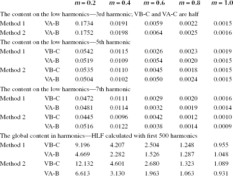
Source: Blaabjerg F., Kragh, H., Neacsu, D.O., and Pedersen, J.K. 1997. Comparison of modulation strategies for B4-inverter. EPE ’97, vol. 2, pp. 378–385.
TABLE 12.3
Considering Individual Voltages VD1, VD2 on Capacitors
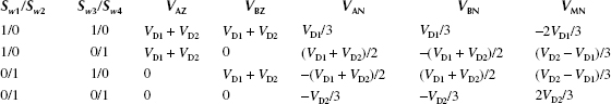
Chapter 5 has shown that variations of the DC bus voltage can be corrected by a proper adjustment of the SVM algorithm through a feed-forward compensation. The same general concept can be applied to the B4 inverter as well. In this respect, Table 12.1 is rewritten in Table 12.3, based on individual voltages on DC capacitors.
Now, we can rewrite Equation 12.20 by taking into account these values.
{t2=3VsVD1+VD2⋅Ts⋅cos ϕ−VD2−VD1VD1+VD2⋅Tst1=12[Ts−3⋅VsVD1+VD2⋅Ts⋅cos ϕ+√3⋅VsVD1+VD2⋅Ts⋅sin ϕ]t3=12⋅[Ts−3⋅VsVD1+VD2⋅Ts⋅cosϕ+√3⋅VsVD1+VD2⋅Ts⋅sinϕ] |
(12.25) |
The effectiveness of compensation can be understood by observing Figures 12.10 and 12.11.
This example of feed-forward compensation works well before the modulator saturates or tends to go in overmodulation. In other words, the time constants calculated with Equation 12.20 should remain positive at any operation point. Let us note ΔV as the absolute value of the ripple within any of the V1 or V2 and RV the normalized value of this ripple:
(12.26) |

FIGURE 12.10 Vector decomposition.
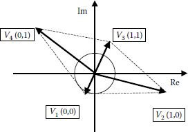
FIGURE 12.11 Deformation of the active vectors due to ripple in the DC bus voltages.
After some calculation, these limits can be computed as
(12.27) |
Graphical representation of these constraints defines the maximum operational range of this feed-forward method (Figure 12.12).
12.3 TWO-LEG CONVERTER USED IN FEEDING A TWO-PHASE IM
Two-phase IMs (induction machines) are used in several low-power applications around or below 1 kW, especially in automation equipment. They have a reduced starting torque, when compared to the DC machines, linear control characteristics, and can be controlled through advanced methods such as field-orientation. The major drawbacks are the reduced efficiency and power factors.
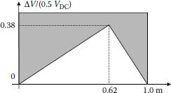
FIGURE 12.12 Maximum correctable ripple by the proposed method.
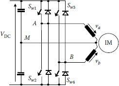
FIGURE 12.13 Two-phase motor drive.
A two-phase inverter with the same power stage as the two-leg inverter (B4) is used for feeding this motor drive (Figure 12.13). This inverter can be supplied from a single-phase diode rectifier suitable to this power level. PWM operation of the IGBT or MOSFET devices building the two-phase inverter ensures variation of both frequency and magnitude of the output voltages. These voltages should be 90o out of phase for a proper torque production within the induction motor. Each inverter leg is PWM-operated between voltage levels of (–VDC/2) and (VDC/2) as shown in Figure 12.14.
The advent of hybrid and electric vehicles opened the door to an impressive development of power electronics solutions for the automotive market. The typical motor drive connection to a high voltage battery pack is shown in Figure 12.15. It consists of a boost (step-up) converter able to increase and regulate the battery voltage to a certain established value. The second stage is a single-phase or a three-phase inverter able to generate a controlled waveform with a high content in fundamental.
The efficiency and cost are driving automotive applications and this supported the appearance of a new inverter topology able to minimize the component count. Both the boost and inverter functions are achieved within the same power stage that is usually called Z-source converter [21,22] (Figure 12.16). This new converter introduces additional zero vector states. During the zero-states from the conventional inverter operation, the DC link is short-circuited like within the operation of a current source converter. Hence the “Z-source” name. When all IGBTs are short-circuited across the DC link (shoot-through), the entire converter works like a boost converter, allowing an increase of the current through the inductors. During the conventional active states of the inverter operation, the DC side voltage equals 2*Vcap – Vbatt, and that is supposed to be regulated by the boost interval. The voltage across capacitors is increased by the current from the two boost inductors even if the load current also acts against the charging of the capacitors.

FIGURE 12.14 Significant waveforms at control of a two phase motor drive with 4 kHz switching frequency. Waveforms shown for m = 0.5 and 50 Hz fundamental.

FIGURE 12.15 Typical dual-stage automotive motor drive.
Waveforms of Figure 12.17 show the quite large second harmonics present in the capacitor voltage, inherent for the operation of a single-phase inverter. A detail of the control signals is shown in Figure 12.18.
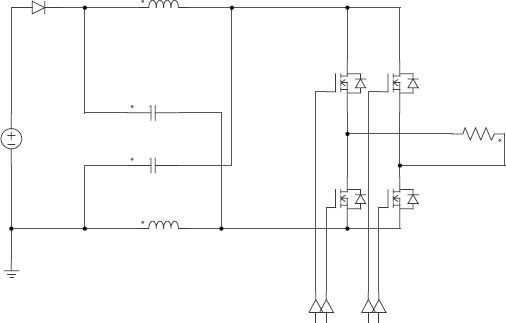
FIGURE 12.16 The Z-source inverter (single-phase version).
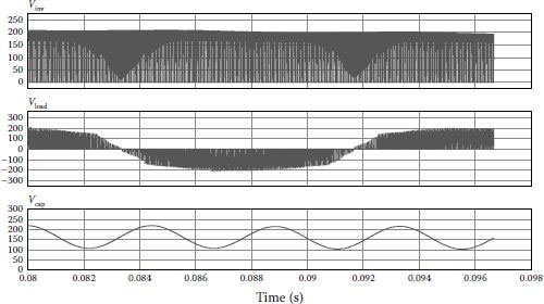
FIGURE 12.17 Waveforms for the generation of 120 Vac from a 120 Vdc battery. The output passive LPF filter is not shown (C = 1 mF, L = 0.5 mH, fsw = 10 kHz, sinusoidal modulation).
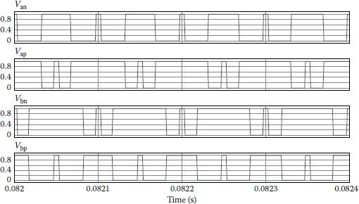
FIGURE 12.18 Zoom on the control signals for the IGBT devices.
The design reduces to the proper sizing of the short-circuit interval along with the conventional sinusoidal modulation control. The peak value of the fundamental of the output voltage yields:
(12.28) |
where Vinv is the voltage at the input of the power converter stage. This is like the output of a boost converter and can be calculated from:
(12.29) |
where To is the shoot-through time interval over a switching cycle T, or D = To/T is the shoot-through duty ratio. Hence, one can define a global voltage gain as:
(12.30) |
The boost factor B is limited by the modulation index M, since a large modulation index M will decrease the available zero-state interval and allow an even shorter shoot-through interval (Figure 12.19).
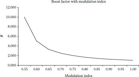
FIGURE 12.19 Maximum ideal boost factor (Bmax) at different modulation index (M).
For this reason, improved control solutions have been proposed over the years to increase the available boost factor [22]. An alternative design can consider generation of the desired output voltage from a larger Vinv voltage, that is a lower modulation index M and a larger boost factor B. However, the product B*M yields is also limited.
During the last 20 years of emerging development in power converters, engineers have tried to explore new three-phase solutions for energy conversion. Several topologies are presented in this chapter and they are intended to open new ideas in design of power converters. Each of these solutions has advantages and disadvantages that make them usable in special applications only.
1. Covic, G.A., Peters, G.L., and Boys, J.T. 1995. An improved single phase to three phase converter for low cost AC motor drives. Proceedings of PEDS’95, Singapore, vol. 1, pp. 549–554.
2. Eastham, J.F., Daniels, A.R., and Lipcynski, R.T. 1980. A novel power inverter configuration. IEEE IAS 2, 748–751.
3. van Der Broeck, H.W. and Van Wyk, J.D. 1984. A comparative investigation of a three-phase induction machine drive with a component minimized voltage-fed inverter under different control options. IEEE Trans. IA 20, 309–320.
4. van Der Broeck, H.W. and Skudelny, H.C. 1988. Analytical analysis of the harmonic effects of a PWM AC/AC drive. IEEE Trans. PE 3(2), 216–223.
5. Blaabjerg, F., Freysson, S., Hansen, H.H., and Hansen, S. 1995. A new optimized space vector modulation strategy for a component minimized voltage source inverter. IEEE APEC 2, 577–585.
6. Blaabjerg, F., Freysson, S., Hansen, H.H., and Hansen, S. 1995. Comparison of a space-vector modulation strategy for a three-phase standard and a component minimized voltage source inverter. Proceedings of EPE’95, vol. 1, 806–813.
7. Blaabjerg, F., Neacsu, D.O., and Pedersen, J.K. 1997. Adaptive SVM to compensate DC Link voltage ripple for component minimized voltage source inverters. IEEE PESC 1, 580–589.
8. Blaabjerg F., Kragh, H., Neacsu, D.O., and Pedersen, J.K. 1997. Comparison of modulation strategies for B4-inverter. EPE’97, vol. 2, pp. 378–385.
9. Jacobina, C.B., da Silva E.R.C., Lima, A.M.N., and Ribeiro, R.L.A. 1995. Vector and scalar control of a four switch three phase inverter. IEEE IAS 3, 2422–2429.
10. Kim, G.T. and Lipo, T.A. 1995. VSI-PWM inverter/rectifier system with a reduced switch count. IEEE IAS Thirteenth Annual Meeting, Orlando, FL, USA, vol. 3, pp. 2327–2332, 8–12 October.
11. Ribeiro, R.L.A., Jacobina, C.B., da Silva, E.R.C., and Lima, A.M.N. 1996. AC/AC converter with four switch three-phase structures. IEEE PESC 1, 134–139.
12. Alexa, D. 1995. Static frequency converter with double-branch inverter for supplying three phase asynchronous motors. EPE J. 5(1), 23–26.
13. Enjeti, P. and Rahman, A. 1993. A new single-phase to three-phase converter with active input current sharing for low cost AC motor drives. IEEE Trans. Industry Appl. 29(4), 806–813.
14. Pan, C.T., Chen, T.C., Hong, Y.H., and Hung, C.M. 1995. A new DC link converter for induction motor drives. IEEE Trans. EC 10(1), 71–77.
15. Neacsu, D.O., Gatlan, C., and Gatlan, L. 1999. A three-phase sinusoidal current rectifier with three unidirectional switches and input transformer. EPE’99, September 2–4.
16. Neacsu, D.O. 1999. Current-controlled AC/AC voltage source matrix converter for open winding induction machine drives. Proceedings of the 25th Annual Conference of the IEEE Industrial Electronics Society, San Jose, CA, USA, vol. 2, pp. 921–926, 29 November–3 December, 1999.
17. Welchko, B. and Lipo, T.A. 2001. A novel variable frequency three-phase induction motor drive system using only three-switches. IEEE Trans. IA. 37(6), 1739–1745.
18. Ziogas, P.D., Vicenti, D., and Joos, G. 1992. A practical PWM AC controller topology. Conference Record of the 1992 IEEE IAS Tenth Annual Meeting, IEEE-IAS, Houston, TX, USA, pp. 880–887, 3–5 October.
19. Lee, J.Y. and Sun, Y.Y. 1986. Adaptive harmonic control in PWM inverters with fluctuating input voltage. IEEE Trans. IE 33(1), 92–98.
20. Enjeti, P. and Shireen, W. 1992. A new technique to reject DC link voltage ripple for inverters operating on programmed PWM waveforms. IEEE Trans. PE 7(1), 171–179.
21. Peng, F.Z., 2003. The Z-source inverter. IEEE Trans. Industry Appl. 39(2), 504–510.
22. Peng, F.Z., Shen, M., and Qian, Z. 2005. Maximum boost control of the Z-source inverter. IEEE Trans. Power Electron. 20(4), 833–838.