
Chapter 15
EMI Standards and Measurements
This chapter discusses typical applicable standards for electromagnetic interference (EMI) compliance, basic measurement techniques and diagnostic tools. It details the mandatory limits for conducted and radiated EMI as per CISPR-22 and FCC (Federal Communications Commission) Part 15. Peak, quasi-peak, and average limits are explained. Common mode and differential mode noise concepts are introduced. The Line Impedance Stabilization Network (LISN) is described. Ways to separate common mode and differential mode components for diagnostic purposes are also presented.
Part 1: Overview and Limits
Sooner or later, every power supply designer finds out the hard way that if anything has the potential to cause a return to the drawing board at the very last moment, it is either a thermal issue, a safety-related issue, or a stubborn EMI (electromagnetic interference) problem. Of these, EMI may be the least predictable and time-bound of all. It turns out to be a veritable “balloon” — if we try to “push” in the emissions spectrum at one frequency, it “bulges” out at another. If we manage to achieve compliance with conducted emission limits, we may find it was at the expense of radiated limits, and so on.
EMI in power supplies is admittedly a challenging area, partly because a lot of uncharacterized parasitics enter the stage, each vying for attention. So, bench tweaking is not going to be completely avoidable. But with a clear insight into the principles, any major redesign should never be required. We have to be cautious however, in applying the terminology and concepts relating to EMI from the area of digital networks (signal integrity issues), directly to switching power supplies. Sure there are great similarities, but the devil is in the details.
The Standards
Electromagnetic interference (EMI) is just one aspect of the area of electromagnetic compatibility (EMC, see Figure 15.1). In our electromagnetic world, all electrical devices need to coexist with each other, and be “good neighbors” — not causing too much interference to others, and not being overly sensitive to others’ interference either. For example, we need to assure a prospective buyer that his or her new set-top box is not going to malfunction whenever someone in the adjacent building just turns on an electric shaver or vacuum cleaner. Both aspects of EMC, emissions and susceptibility, are, therefore, regulated by various international EMC laws. These are the two sides of the coin called EMC. As we can easily foresee, switching power supplies are best labeled as culprits, not victims.
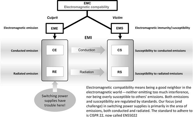
Figure 15.1: The EMI/EMC “tree” (emissions and susceptibility).
Recognizing that the local environment plays a role in defining the amount of received interference and its level of acceptability, EMI limits are split into two basic application categories.
• Class A, corresponding to commercial/industrial equipment/environment. Their corresponding limits are relatively relaxed.
• Class B, corresponding to domestic or residential equipment. Their corresponding limits are relatively stringent.
Rather broadly stated, Class B limits are roughly about 10 dB lower than Class A limits. This represents a ratio of about 1:3 in terms of the amplitudes of the emission levels (20×log(3)≈10 dB).
Note that when in doubt as to where a certain piece of equipment may be used eventually, we need to design it for Class B requirements.
There is another major compliance requirement for us to be able to sell a product in the marketplace, and that is based on safety. In many countries, EMC and safety compliance are clubbed together under a regional conformity mark. The CE mark (i.e., European Conformity mark) is one such example. Another is the CCC mark (China Compulsory Certification, required by the People’s Republic of China. i.e.. mainland China). Such marks indicate compliance to both the required EMC standard and the safety standard.
The generally accepted international EMI standard has been historically called CISPR-22. In the European Union, applicable products need to comply with EN55022 (this is basically just CISPR-22 after getting ratified and mandated for use in the European Union). On the other hand, the generally accepted international safety standard is IEC 60950-1 (historically called IEC 950, then IEC 60950, and so on). In Europe, applicable products need to comply with EN60950 (the ‘Low Voltage Directive’), which is essentially the same as IEC 60950-1 (after getting ratified and passed into law). Though there are certain parts of Europe, especially the Scandinavian regions, where compliance to IEC 60950-1 is required with some additional requirements referred to as national/regional “deviations.” In the US, the IEC 60950-1 safety standard has been adopted as UL 60950-1 (currently in 2nd Edition).
As indicated, in the US, the issues of safety and EMC are taken up separately, and there is no combined conformity mark. The “UL mark” (Underwriters Laboratory Inc.) indicates compliance to product safety standards, whereas “FCC certification” (Federal Communications Commission) reflects compliance with EMI standards.
There are differences between the EMI standard CISPR-22 and the US standard (FCC Part 15). We will discuss the differences later. But very generally speaking, it is said that if a power supply meets CISPR-22, it will likely meet FCC standards. Furthermore, FCC often accepts certification to CISPR-22. So, in general, CISPR-22 has become the underlying standard to comply with across the world (for IT-related equipment and power supplies).
EMI Limits
In Figure 15.2, we have plotted out the EMI limits imposed by the CISPR-22 and FCC standards. We see there are “conducted” EMI limits expressed in μV or dB μV as a function of frequency. This is the actual voltage drop measured across a certain resistor within special receiving equipment as we will see. Then there are “radiated” EMI limits expressed in μV/m or dB μV/m, representing the measured electric field “E” at a specified distance from the emitter (culprit), measured by an antenna in a special chamber. Why measure only electric fields, not magnetic fields? Because the two are proportional to each other at great distances as we will learn.
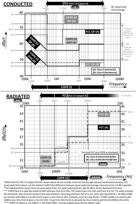
Figure 15.2: Plots of conducted and radiated EMI limits as per CISPR-22 and FCC part 15.
In Figure 15.3, we have collected the numbers from Figure 15.2 into easy lookup tables. Alongside, are sample calculations to show how to calculate μV from dB μV and vice versa. We still need to explain certain key terms contained in these two figures and in the accompanying sample calculations. We will do that further below.
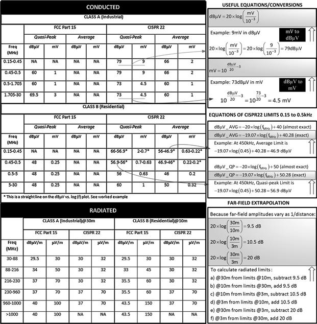
Figure 15.3: Tables of conducted and radiated EMI limits and useful equations.
We observe that standard conducted EMI emission limits are typically only up to 30 MHz. We can ask — why weren’t the limits set higher? The reason is that by 30 MHz, any conducted noise is expected to automatically suffer severe attenuation in the mains wiring, and therefore won’t really be able to travel far enough to cause interference “further down the road.” However, since cables can radiate and send electromagnetic fields over great distances, typical EMI radiation limits cover the range from 30 MHz to 1 GHz.
Comparing the (conducted emissions) Class A quasi-peak limits of FCC and the CISPR-22 in Figures 15.2 and 15.3, and then doing the very same comparison for the Class B limits, we can justifiably ask — do the numbers imply that the FCC standards are more stringent than those of CISPR-22? Not really. The first difference is that FCC measurements are done at much lower (US) line voltage levels, whereas CISPR measurements are done at roughly twice that voltage. So, we may be comparing apples to oranges. Further, though FCC has no defined average detection limits (only quasi-peak), the language allows for a relaxation of the quasi-peak limits (by 13 dB) if a quasi-peak reading exceeds the average by more than 6 dB. Therefore, practically speaking, equipment compliant to CISPR will very likely be found compliant to FCC limits.
Some Cost-Related Rules-of-Thumb
A brief look at possible costs:
• The FCC spectrum for digital equipment (currently) begins at 450 kHz, while the equivalent CISPR/EN regulations start at 150 kHz. So, FCC compliance can be achieved with a relatively small and inexpensive filter.
• CISPR/EN Class A compliance often requires a filter with at least twice the volume of the FCC-level unit. This filter can therefore be up to 50% more expensive.
• CISPR/EN Class B compliance can require a filter with 3–10 times the volume of the FCC unit, and could cost up to four times more.
Note: CISPR limits apply to line voltages of 230 VAC, whereas FCC limits are tested at US line voltage (115 VAC). For a given output power, the input operating current is higher if the input voltage is less. Therefore, if any equipment is designed to operate at US line voltages, thicker copper is required in the filter chokes, and that is somewhat of a cost adder.
EMI for Subassemblies
EMC is generally considered a system-level concern, since from the legal perspective, it applies only to the end-equipment. So, a component power supply (also called an “OEM” power supply or a “subassembly,” e.g., the one inside our desktop computer) does not usually have to meet any EMI/EMC standard per se, unlike a stand-alone power supply. The ultimate EMC responsibility rests with the system manufacturer. However, take the case of a component off-line power supply (the front-end power converter for the system). Here, a major component of the observed EMI measured at the input of the system will clearly be coming from the power supply. So, it certainly won’t help if the power supply itself is producing more EMI than the limits that apply to the overall system. We should then keep in mind that when the power supply is integrated with the equipment, there are always some hard-to-predict interactions between the power supply and the rest of the system — through the connectors, wiring, chassis, grounding, and so on. So, the final EMI spectrum is not necessarily just the arithmetic sum (in dB) of the different subassemblies. Keeping this in mind, the system manufacturer would most likely call out for a front-end converter to maintain its EMI to less than 6–10 dB below the legal limits. That would usually leave enough headroom for the rest of the system, as also for unexpected interactions between the power supply and the rest of the system. In addition, certification labs themselves may require submitted prototypes to be at least 2–3 dB below certification limits — so as to leave margin for variations in subsequent production lots. Summing all this up — the practical resulting situation for (front-end) OEM power supplies is simply this — yes, they don’t need to comply with the legal EMI limits, in fact they need to be better (than component power supplies).
What about DC–DC converters that happen to be positioned deep inside the equipment (like point of load converters and bricks)? Again, there are no legally applicable EMI/EMC standards for these per se. Further, since they are likely to be preceded by various circuits and filters, surge suppressors, fuses, capacitors, inrush limiters, and so on (e.g., inside the front-end AC–DC power supply too), there is usually an adequate (and fortuitous) EMI barrier already present, that prevents noise from the DC–DC converter from getting on to the AC mains lines via conduction. Further, if we assume there is in effect an EMI radiation shield present (e.g., the grounded metal enclosure), radiated EMI may also not be of great concern. Therefore, typically, for low-power on-board DC–DC converters, no dedicated input filter stages may ever be required. However, if such a filter does become necessary, it can usually just be a simple single-stage LC circuit — possibly even using a small ferrite bead inductor as the “L” of the LC filter. Sometimes, just one such LC filter stage may be good enough to service several paralleled DC–DC converters.
Despite the above natural EMI buffers that are usually present, manufacturers of DC–DC converter modules are often going through the trouble of profiling the EMI spectrum present at the (unfiltered) inputs of their products. The purpose is that, whether legally required or not, the information will come in handy for the system designer when he or she makes EMI-related decisions later. Further, very often nowadays, even the outputs of DC–DC converters are being EMI-profiled.
Electromagnetic Waves and Fields
Light, radio-frequency (RF) waves, infrared (IR) radiation, microwaves, and so on, are all electromagnetic waves. For all these, the basic relationship connecting their wavelength λ (in m), their frequency f (in Hz), and the speed of the wave u in the medium of propagation (in m/s), is given by λ=u/f. For a wave propagating in free space (or air), the speed u is called “c” and has the value 3×10⁸ m/s. An easy form to remember is
![]()
The ratio c/u is always greater than 1, and is called the index of refraction of the material (through which the wave travels at the speed u). Note that though c is popularly called the velocity of light, it is the same for any electromagnetic wave. It can be shown that c=1/√(μoεo), where μo is the permeability of free space (vacuum or air) and εo is the permittivity of free space. μo and εo are fundamental constants, since they represent the properties of our universe.
We may remember from our physics class that if a piece of electronic equipment has any dimension close to λ/4, it can end up radiating (or receiving) the corresponding frequency very effectively. This is the principle behind a radio antenna. (Note that a symmetrical antenna has a total physical length of λ/2, but that comes from balanced sections of length λ/4 placed on each side). So, what if an antenna is much shorter than the “optimum length” of λ/4? Antennas are actually quite effective down to less than λ/10 — which explains why we can pick up almost all the FM stations well enough from a (fixed length) whip antenna on our car. What if the antenna is much longer than λ/4? In that case, we can intuitively consider the antenna as being in effect, clamped at λ/4 — the remaining length is basically superfluous. Therefore, it seems wise to never judge an antenna by its length alone, and we need to keep this in mind especially when designing a PCB for a switching power supply. There, we must minimize large areas of copper with swinging voltages on them (e.g., the switching node), and also reduce the enclosed area of any current loop, especially those containing high-frequency harmonics. This was discussed in Chapter 10.
When we plug a piece of equipment into the AC power lines, its input cable (AC line cord) can combine with the wiring of the building to form a giant antenna. This can produce strong radiated interference that can affect the operation of other devices in the vicinity. In addition to the radiation process, the emissions can also just keep conducting down the mains wiring, thereby directly entering other similarly plugged-in devices. Therefore, there are distinct radiated emission limits and conducted emission limits specified within all EMI regulatory standards.
We have realized that it would be a mistake to jump to the conclusion that a certain cable length or PCB (printed circuit board) trace is either “too short” or “too long,” and therefore not contributing to a certain stubborn EMI peak that we may be observing. Further, we should keep in mind that any antenna is as good a receiver, as it is a transmitter. So, we could have a situation where radiation is originally generated by the output cables, but then picked up by the input cables (by radiation), from which point onward it gets conducted into the wiring of the building (or/and radiated once again). In fact, we will find that the input and output cables are often responsible for a lot of high-frequency EMI noise, both in the radiated spectrum and the conducted spectrum.
Concerns about cable length take on a whole new meaning when they are coupled with circuits containing modern high-speed digital chips. Such chips are themselves powerful EMI emitters, but with the help of inadvertent antennas like the surrounding PCB traces and cables, and also with the inadvertent help of various board, component, and enclosure parasitics, they can put on quite a show, courtesy Maxwell.
Maxwell showed that whenever an electric field (the “E-field” — dimensions V/m) varies with time it produces a magnetic field (the “H-field” — dimensions A/m), and vice versa. In fact, the better-known Faraday’s law of induction (without which no transformer in the world would exist) is actually the first of the set of four Maxwell’s unifying equations. So, we learn that the E and H fields appear simultaneously, the moment the original magnetic or electric source has a time variance. At some distance away, these fields combine to form an electromagnetic wave — that propagates out into space (at the speed of light).
We can ask — what really makes modern digital chips, and modern switching converters, so much worse than their predecessors, from the standpoint of EMI? That is because of the escalating frequencies involved. Smaller and smaller PCB traces and lead lengths can become effective antenna at very high frequencies. So, we are nowadays getting painfully aware of the fact that as the frequency increases, the intensity of these fields (at a certain distance) also increases. Note however, that when talking about switching power converters, the “frequency” that we are talking about is not necessarily the basic PWM switching frequency (which is only of the order of say 100–1000 kHz). We are referring more to the exceedingly fast transition times — which are of the order of 10–100 ns. The Fourier analysis of such a switching waveform will reveal a large amount of very high-frequency content, associated with the actual switch transitions. These sharp voltage and current edges are what really exacerbate the problem as we will see in Chapter 18.
Maxwell’s equations are usually written out in a way that doesn’t fully reveal the following fact clearly: it really does not matter whether we are talking about waveforms of switched voltages (time-varying E-fields) or of switched currents (time-varying H-fields) — eventually, their respective equations are complementary, and very similar. More important, these two fields become proportional to each other at a large distance away, constituting an electromagnetic wave, one that becomes self-sustaining and can, therefore, travel great distances on its own (yes, across galaxies). It also follows that if we “kill” one component of an electromagnetic wave (either its E-field or H-field), we will manage to kill the entire electromagnetic wave. Therefore, we often use RF (radio-frequency) shielding or electromagnetic shielding. However, if we want to suppress slowly varying fields, and/or near-fields, we often use electrostatic shields and/or magnetic shields.
To go back to our physics class for a moment, in general, circuits that cause fields can be sorted into four basic classes:
The electrostatic class is simply a fixed distribution of charges. Since the charges do not move, no current flows. The basic building block here is the “charge dipole,” where two equal and opposite charges are placed a certain distance apart (one may be at infinity), or we could have a wire held at some fixed voltage. In either case, we have an electric field E that does not vary with time. There is no associated magnetic field (H is zero) based on Maxwell’s equations. There is therefore no concept of wave impedance here, and the ratio of E to H is infinite.
Magnetostatic circuits consist of DC current loops. This is the dual of the electrostatic case. There is a constant magnetic field H present that is time invariant. Field information doesn’t propagate in this case either.
The third class above is a time-variant electric circuit. We could start by thinking of a slowly varying electrostatic circuit. Consider these to be more or less equivalent cases:
(a) A charge dipole where the charges vary sinusoidally.
(b) A current element where current flows back and forth sinusoidally along a line (charges would build up and reverse at the ends, so this is equivalent to the previous example).
(c) Any collection of open-ended wires driven by arbitrary voltage sources, including dipole and whip antennas, as well as low-speed leads exiting circuit boards and driven by common mode voltages (“common mode” is explained a little later).
(d) A short, sinusoidally varying current element known as a “Hertzian dipole.” “Short” just means small in comparison with a wavelength at the drive frequency. If it is short, we can assume the current is uniform over the wire at any instant.
By Maxwell’s laws close to such an electric source, we get not only an electric field, but also an associated magnetic field. The electric field contains components that vary as 1/r3, 1/r2, and 1/r, where r is the distance from the dipole. The magnetic field contains components that vary as 1/r2, and 1/r. Far away, the 1/r2 and 1/r3 components have decayed sharply due to the increasing distance. Finally, both E and H fields are left with an approximate 1/r variation, so their ratio E/H becomes a constant. Note that from our physics class, we remember that the field from a point source (charged particle) varies as 1/r2. That is clearly not true for time-varying fields.
The dual to the Hertzian dipole in our fourth case above, is a sinusoidally excited current loop. The electric and magnetic fields for a sinusoidally driven infinitesimal current loop mirror those for the Hertzian dipole. Here, the near field magnetic field exhibits 1/r3, 1/r2, and 1/r behavior, while the electric strength has components that fall off as 1/r2 and 1/r. Far away, both E and H exhibit 1/r behavior.
The ratio of the E and H fields is called the wave impedance. Far away, it is a constant. This is shown in Figure 15.4. In general, the proportionality constant between E and H depends on the material of propagation, and equals E/H=√(μ/ε), where μ in this case is the (absolute) permeability of the material and ε its permittivity. Note that ε is the electrical analog of the magnetic parameter μ that as we know describes the extent to which a given material allows itself to become magnetized by an external magnetic field. We also note that the units of E are V/m, and H is A/m. Therefore, the ratio E/H has the units V/A, which is simply resistance (ohms). If the material of propagation is air or vacuum (free space), E/H=√(μo/εo)=120×π=377 ohms. E/H=377 Ω is called the wave impedance in free space, or the intrinsic impedance of free space.
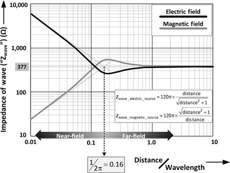
Figure 15.4: Electric and magnetic impedances in free space.
From Figure 15.4, it also becomes clear why it is often colloquially said that “electric fields have high impedance,” whereas “magnetic fields have low impedance.” A small circular current loop of trace on a PCB produces magnetic fields, but a strip of copper or metal with a swinging voltage on it (e.g., a heatsink) forms a source of electric fields. Of course, once there is time variance involved, the H-field leads to an associated E-field, and an E-field produces H-fields. At a great distance, the E and H fields become proportional to each other and form an electromagnetic wave. We define the boundary between what is considered a “far-field” and what is a “near field,” as the distance ~λ/6~0.16λ away from the EMI source.
Extrapolation
We see that far fields decay as per 1/r (inversely proportional to distance). So, if the field at distance r1 is E1 and at r2 it is E2, they are related as
![]()
The ratio of the fields expressed in decibels, is by definition
![]()
For example, if x1 is 10 m, and x2 is 100 m, the field strengths are different by
![]()
Or E1 is 20 dB greater than E2. Alternatively expressed, fields decay as per 1/r, or 20 dB per decade (of distance). So, as distance changes by a factor of 10, the field falls by 20 dB — provided it is a far-field. And if we can confirm that it indeed is a far-field, then the amplitude of the field becomes entirely predictable. For example, if we know the far-field at a given point in space, we can use the preceding physics to accurately predict its value at any another point in space (again, provided that point is also within the far-field region). We call this technique “inverse linear distance extrapolation.”
In standard radiated EMI tests, the specified measurement range of frequencies is 30 MHz and above (usually up to 1 GHz). We ask: from what distance can these frequencies be considered far-fields? For 30 MHz, the distance in meters that marks the boundary between near-field and far-field is, as per Figure 15.4
![]()
For 1 GHz it is proportionately smaller. In other words, if an antenna is placed at least 1.6 m away from the radiating source (say at 3 m), and we measure the field at that point, we can then use inverse linear distance extrapolation to predict the field amplitude at any other (further) distance — say 10 m, 30 m, and so on.
For confirming compliance to Class B limits, FCC generally requires the antenna distance to be 3 m, whereas CISPR requires 10 m. For confirming compliance to Class A limits, FCC specifies the distance to be 10 m, whereas CISPR requires 30 m. The good news is that 3 m is certainly far-field for all frequencies in the radiated range of interest, and we should be able to apply extrapolation to ultimately compare apples to apples. These normalized limits are shown side by side in Figure 15.2. Here, we have done two things to the original FCC limits. (A) The original FCC limits are in μV and μV/m, not dB μV and dB μV/m as used by CISPR-22. In Figure 15.3, we have included sample calculations showing how we can convert between the two. (B) We have extrapolated the Class A FCC limits to 30 m and the Class B FCC limits to 10 m, to compare them with the CISPR limits.
Note: From Figure 15.2, it might seem that both Class A and Class B FCC limits are identical, at 29.5 dB μV/m, over the range 30–88 MHz. But don’t forget that Class A limits are shown at 30 m, whereas Class B limits are at 10 m. We know from the extrapolation factor calculations in Figure 15.3 that the field at 30 m will be exactly 9.5 dB lower than its value at 10 m. So, in fact, the FCC Class A limits are exactly 9.5 dB (~10 dB) higher, and therefore more relaxed than FCC Class B limits, when compared at the same distance from the EMI emitter.
Note: The near-field/far-field definition in Figure 15.4 assumes the EMI emitter is a point source. Therefore, especially in the case of a 3-m test, some further validation may be necessary to prove that we really do have only far-fields.
Quasi-Peak, Average, and Peak Measurements
We have not yet explained what the rationale is behind the two types of limits — average and quasi-peak (for the conducted EMI limits in Figure 15.2).
Historically, quasi-peak (or almost-peak) was meant to simulate human responses to noise. Humans have a slowly increasing level of aggravation or annoyance to a persistent disturbance. Therefore, to simulate this (subjective) response, there are built-in attack and release rates in quasi-peak detection. Conceptually, it works like a peak detector followed by a lossy integrator. Applied to a switching power supply, we note that in quasi-peak detection, the signal level is effectively weighted according to the repetition frequency of the spectral components constituting the signal. So, the result of a quasi-peak measurement will always be dependent on the repetition rate. The higher this repetition frequency (e.g., switching frequency), the higher the measured quasi-peak level.
Because of the finite charge and discharge time constants involved in quasi-peak detection, the spectrum analyzer must sweep considerably slower in quasi-peak setting. The entire EMI measurement process thus becomes very slow. To avoid delay, peak detection can be carried out, as it is much faster. However, we will then always get the highest reading, followed by quasi-peak and then by average (see Figure 15.5).
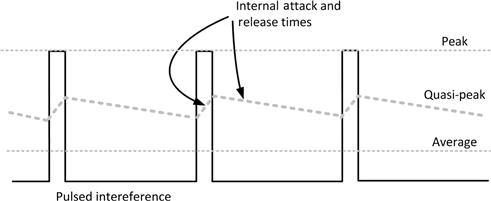
Figure 15.5: Average, quasi-peak, and peak readings of a pulsed wave.
Part 2: Measurements of Conducted EMI
Differential Mode and Common Mode Noise
Here, we clarify the concepts of “common mode” and “differential mode” noise in conducted EMI. Initially, we are going to stick to more conventional descriptions of these parameters. But in Chapter 16, we will start discussing certain nuances/differences that can arise in applying the concepts to the area of power conversion.
Conducted emissions fall into two basic categories
• Differential mode (DM), also called symmetric mode or normal mode.
• Common mode (CM), also called asymmetric mode or ground leakage mode.
Looking at Figure 15.6, “L” stands for Live (or “Line” or “Phase”), “N” for Neutral, and “E” is the “Safety Ground” or simply, “Earth” wire. “EUT” stands for Equipment Under Test. Note that the Earth is shown represented by the IEC symbol for Protective Earth (ground with a circle around it), occasionally labeled “PE” in literature. The DM noise generator is across the L and N pair. It tries to push/pull a current Idm through these two wires. No current flows through the Earth connection on account of this noise source.
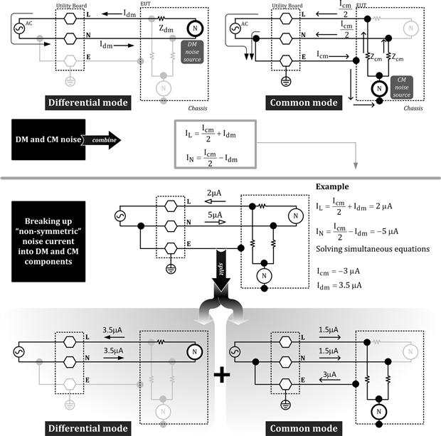
Figure 15.6: Differential and common mode noise with a worked example.
To avoid confusion, we should note that the net common mode current going through the Earth is called “Icm” in our case (Icm/2 in each line). However, in related literature, this is often called “2Icm” (Icm in each line).
Note: There is nothing special about the DM noise current direction as indicated in the figure. It can well be the other way around — that is, going in through either L or N, and coming out of the other. In off-line power supplies, we will see that in fact, the direction reverses every AC half cycle.
Note: The designer may realize that the basic AC input operating current of the power supply is also differential in that sense — since it flows in through one of the L or N wires and leaves by the other. However, the Idm shown in Figure 15.6 does not include this component. That is because the operating current, though differential, is not considered to be “noise.” Further, its main components (and also its key harmonics) are of very low-frequency, being virtually DC, and well below the range of standard conducted EMI limit curves (150 kHz to 30 MHz). The standards regulating line harmonics were discussed in Chapter 14. However, it must not be forgotten that the operating current of the power supply can DC-bias the EMI chokes, and can thereby adversely affect the performance of the EMI filtering and also of any current probes being used to gather data. So, though we can certainly ignore AC (line) while discussing EMI, we should realize it can have a major though indirect effect on the performance of the filter.
In Figure 15.6, the CM noise source is shown connected at one end to Earth. On its other side, it is assumed that the noise source sees equal impedances on each of the L and N lines. It will therefore drive equal noise currents into these two wires, and in the same direction. We realize that if the impedances are unbalanced, we will get “mixed mode” (MM) noise current distribution (in the L and N wires). And that is in fact a common scenario in actual power supplies. Note that this mode is equivalent to a mixture of true-CM noise mixed with some DM noise as demonstrated in the worked example in Figure 15.6.
Just as common mode noise generated by a power supply flows into the mains wiring, it can also flow into the output. Engineers often instinctively tend to disregard common mode noise present in the output of their power supplies, instead focusing at the input only. But it is important to understand what both components are, for the following two key reasons:
(a) As mentioned previously, in telecom networks and distributed power applications, the common mode noise will use the long output cables as a giant antenna.
Also, by their very nature, common mode currents in power supplies usually have much higher high-frequency content than differential mode currents. They therefore also have the capacity to cause severe radiation (besides causing inductive and capacitive coupling to nearby components and circuits). An oft-repeated rule-of-thumb is that a mere 5 μA of common mode current in a 1 m length of wire can cause FCC Class B radiation limits to be violated. For FCC Class A limits this number goes up to 15 μA. Note also that the shortest standard AC power cord is 1 m in length. We thus see the importance of reducing common mode noise currents both at the input and output of a power supply.
(b) In terms of qualifying the power supply itself, engineers typically have a target spec for output noise and ripple measurement. That is actually a differential measurement. Engineers spend a long time trying to get the oscilloscope probe positioned correctly on the output terminals (with minimum length of probe ground wire), simply to avoid picking up common mode noise via radiation. But common mode noise can still affect the differential ripple measurement. Because, if the power supply is providing power to a real subsystem (not a resistive “dummy test load”), then looking into the input of this subsystem, we will rarely (if ever), see equal (balanced) impedances (i.e., from each of its input terminals to the Earth ground). So, what really happens is that any “common mode” noise existing previously on the output rails of the power supply, now becomes a differential input voltage ripple (of high frequency). It takes on the profile of mixed mode currents as shown in Figure 15.6. We will see that no amount of common mode rejection ratio (CMRR) in the subsystem will help completely, since the erstwhile pure common mode noise is now partly differential. The subsystem could start misbehaving as a result of that. Summarizing: common mode noise gets converted into differential mode noise if the line impedances are unequal. For the very same reason, even at the input of the power supply, we always use balanced filters. In general, reducing common mode noise at the point of creation is a high priority. But after that, equalizing the line impedances becomes important. The latter can often be achieved by placing balanced filters at the input and output of the power supply, and also at the input of the subsystem that it powers — for example, two inductors, one on each input line, instead of just one inductor.
Note: There is nothing special about showing the CM noise current in Figure 15.6 coming out of the equipment (through both the L and N wires). It could well be in the reverse direction. And like DM noise in an AC–DC power supply, it too could be sloshing back and forth, depending on what part of the incoming AC half cycle we are on, at a given moment.
Note: We will see that in an actual power supply, differential mode noise is initiated by a swinging (pulsating) current — but the DM noise generator is itself closer to a voltage source. On the other hand, common mode noise is initiated by a swinging voltage, but the CM noise generator itself behaves more like a current source. That is actually what makes common mode noise so much more “stubborn” — like any other current source, it demands a path to flow through. And since its path can include the chassis, the enclosure can then become a large high-frequency antenna too.
Measuring Conducted EMI with a LISN
For measuring EMI, we need to use an ISN (Impedance Stabilization Network). In off-line power supplies, this is called a LISN (Line Impedance Stabilization Network) — also called an AMN (Artificial Mains Network) (see Figure 15.7 for a simplified schematic). Note that the LISN, as recommended for CISPR-22 compliance, is detailed in another standard called CISPR-16. It provides the following functions:
• It is a source of clean AC power to the power supply, being virtually transparent to the line frequency component. This allows normal operation of the equipment under test (EUT, e.g., the power supply).
• It blocks any extraneous noise from the AC line from entering the measurement area (by two 50 μH chokes), and thereby keeps it ready for clean measurements on the EUT.
• It similarly blocks noise from the power supply from entering the AC line, and instead, diverts it into the measurement area.
• It blocks the AC line component from entering the measurement area by means of two 0.1 μF blocking capacitors.
• It provides a stable and balanced impedance to the emanating noise, attempting to replicate the typical impedance normally presented by the AC wiring to the noise.
• The diverted noise is then measured by the measurement receiver/spectrum analyzer.
• Most importantly, the LISN makes the measurements repeatable, anywhere in the world.
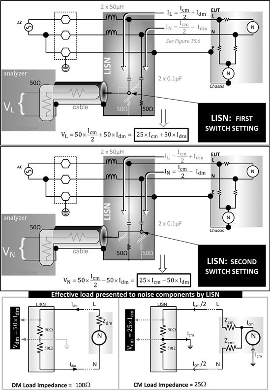
Figure 15.7: Simplified schematic of LISN and the load it presents to the CM and DM noise.
Note that we have implicitly assumed that
• The inductance (50 μH) is low enough not to impede (AC) line current (50/60 Hz) at all — but high enough to be considered “open” over the frequency range of interest (150 kHz to 30 MHz).
• The blocking capacitance (0.1 μF) is low enough not to pass the AC (line) voltage — but high enough to appear as a “dead short” over the frequency range of interest.
The combined noise current is diverted into 50 Ω resistors as seen from Figure 15.7. To ensure signal integrity, the receiver (measuring instrument) is set to 50 Ω impedance setting, and that is what the high-frequency noise “sees” when looking into the coaxial cable. Note that on the LISN, we have two switch settings, one for measuring the voltage across the resistor in one phase (L), and the other position for measuring the other phase (N). But since the receiver already presents 50 Ω to the noise currents on the channel being measured, the discrete 50 Ω resistor is disconnected on that channel. Then, to maintain balance, a discrete 50 Ω resistor is placed on the other channel as indicated in the figure.
In the lower part of Figure 15.7, we follow the paths of the DM and CM components separately, and realize that the LISN presents a load impedance of 100 Ω (two 50 Ω in series) to the DM component, and a load impedance of 25 Ω (two 50 Ω in parallel) to the CM component. Note that in both cases, one of the “two 50 Ω” resistors is discrete, while the other is the input impedance of the receiver.
As we flick the switch on the front panel of the LISN, we will measure the following noise voltages
![]()
![]()
Both the VL scan and the VN scan obviously need to comply individually with the limits in Figure 15.2.
How different can the VL and VN scans be? In fact, the above two equations may have inspired a rather misleading statement in related literature. It is often stated: “if the noise emission is predominantly DM, the VL and VN scans will look almost the same. The scans also look identical if the noise is predominantly CM. And if the VL and VN scans look very different, that implies that both CM and DM emissions are present.” However, in the case of an off-line (AC–DC) power supply, this statement is not true. Because, it would imply that somehow the emissions on the L and N lines are different. However, we know that in any typical off-line power supply (with an input bridge rectifier), the L and N lines are essentially symmetrical — both from the viewpoint of the operating current and, therefore, the noise spectrum. So, every successive AC half cycle, the operating current, and the noise distribution get transposed from one line to the other. True, at any given moment, the noise on L will be quite different from that on N, but when averaged over several AC cycles (as any spectrum analyzer would do), equality (symmetry) is restored. Any remnant differences between the VL and VN scans can be traced back to some undocumented asymmetries between the two halves of the test circuit, or some severe radiation source impinging asymmetrically on the cables, or on traces/wires very close to the inlet of the power supply (between the EMI filter and the AC inlet socket).
In Chapter 17, we will see that the frequency response (sensitivity) of the LISN is not “perfect” because its inductors and blocking caps are not ideally large. Understanding the actual frequency response of the LISN helps us a great deal in designing cost-effective EMI filters.
Simple Math for Estimating Maximum Conducted Noise Currents
From Figures 15.2 and 15.3, we see that over the range 0.15–0.5 MHz, CISPR Class A restricts the average voltage to 2 mV. We already know that the impedance presented by the LISN to the CM noise is 25 Ω. So, if we know voltage and resistance, we know current. In this case the maximum permissible CM current is 2 mV/25 Ω=0.08 mA or 80 μA. This, however, assumes no DM noise component. So, in general, if we assume equal contributions coming from CM and DM noise, we should halve the target to 40 μA. Over the range 0.5–30 MHz, CISPR Class A restricts the voltage to 1 mV, or 40 μA. We can target 20 μA. Similarly, FCC Class A restricts the voltage to 1 mV from 0.45 MHz to 1.7 MHz. Therefore, the maximum permissible CM current is 40 μA over this range. From 1.7 MHz to 30 MHz FCC Class A allows 3 mV, or a maximum of 120 μA, and so on. For DM noise, we should use 100 Ω instead of 25 Ω to calculate the maximum permissible noise current. In Chapter 18, we will do a more detailed calculation.
Separating CM and DM Components for Conducted EMI Diagnostics
We observe that the standards do not require us to measure the CM and DM components individually, but rather a certain sum as described in the preceding equations in Figure 15.7. However, there are times when engineers do want to see both the CM and DM components separately — for troubleshooting and/or diagnostic purposes. So, various people have come up with clever ideas to separate the CM and DM components. Some of these are presented in Figure 15.8.
• The first is a device called the “LISN MATE,” which is quite rare now. It was invented by an engineer named M.J. Nave. It provides about 50 dB attenuation for the DM component, but the CM component comes right through (slightly attenuated — by about 4 dB).
• The next one in the figure is a transformer-based device. It exploits the fact that common mode voltages cannot cause transformer action — because transformer action requires a differential voltage be applied, so as to produce current in the windings, and thereby cause the flux to swing within the core. Unlike the LISN MATE, in this case both CM and DM noise components are outputted.
Note: Both methods above unfortunately require modifications to the standard LISN — because they invoke a certain math between the VL and VN components. However, a LISN normally provides either VL or VN at any given moment — not both (at the same time as required here). We can modify the traditional LISN, but that is not only tricky to do, but also hazardous because of the high voltages involved. Therefore, a completely different approach is to simply buy a LISN explicitly designed for the purpose of providing separate CM and DM noise scans (besides providing the necessary “summed up” scan for achieving compliance).
• Finally, we have shown two current probes, wired up in such a way that they are actually solving two “simultaneous equations” on the L and N wires. They separate the CM and DM components. Note that by doing these two measurements at the same time (using two probes rather than one), we have retained valuable information about the relative phase relationship between the CM and DM components.
Note: The bandwidth and current capability of the current probes used for noise measurements are important. For very high currents (up to thousands of Amperes if necessary), a possible choice is current probes based on the “Rogowski principle.” The output from a Rogowski probe depends not on the instantaneous current enclosed, but on the rate of change of current. So, instead of just placing several turns around the wire to be sensed, as in a typical current transformer, the Rogowski probe effectively takes an air-cored solenoid and then bends that in a circle around the sensed wire (like a doughnut). Such probes are also considered virtually non-invasive. The usual lab active current probes (which also measure DC, and therefore include a Hall sensor), are usually just not suited for these high-bandwidth noise measurements.
Note: When viewing pulse transition times below 100 ns, or emission noise frequencies above a few Megahertz, it is advisable to keep the cable length small. Thereafter, we must terminate the cable at the oscilloscope, or measuring instrument, with a 50 Ω resistor. However, most modern oscilloscopes incorporate a selectable 50 Ω input impedance. Correct termination of cables prevents standing wave effects. Note that, with this 50 Ω termination, the measured voltage is approximately half of what it really is because we essentially have a voltage divider formed by the cable and the terminating resistor. Oscilloscopes will usually automatically correct for this, if they “know” that there is a 50 Ω termination present. Also note that fast-rising pulses can produce spurious ringing, due to high-frequency current crowding on the surface of the cable shield. This can be suppressed by threading the measurement cable through one or more ferrite beads (or toroids). For example, some report that they obtained good results by placing three turns through four ferrite cores of about 1 in. inside diameter, 2 in. outside diameter and 1/2 in. thickness.
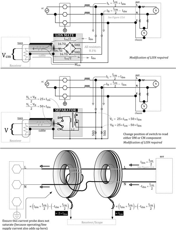
Figure 15.8: Ways to separate CM and DM components for troubleshooting.
In the upper part of Figure 15.9, we show a practical technique to separate that part of the conducted emissions spectrum attributable to radiation pickup occurring within the power supply itself. We see how to identify these as E-fields or H-fields. For this experiment, we need to cut the PCB traces just before the input bridge, and then route the AC power from a canned filter outside the enclosure. The ends of the existing filter are kept either open (to receive E-fields) or connected together through a small loop (for seeing the H-fields). The other end of this EMI filter is then routed as usual to the LISN and spectrum analyzer. We can thus see the “extraneous” radiation-based noise being picked up by the internal EMI filter via radiation inside the power supply. It will give us an indication if a heatsink for example is causing severe E-fields, or if a certain magnetic component is causing severe H-fields. We can also wave a small plate of thick copper (connected to Earth) in suspected areas to see which component may be the actual source of the fields. For analyzing the source of magnetic near-fields, a slab of ferrite (from a typical EMI suppression kit) works better than a copper plate and that can be waved around similarly (no need to Earth it).
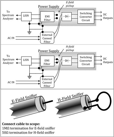
Figure 15.9: Analyzing magnetic and electric field sources inside a power supply and near-field sniffers made from a coaxial cable.
Caution: AC power is NOT to be applied through the LISN in the above experiment. This will cause a serious hazard to the user. Also, any plate/slab must be well-wrapped in insulating tape to prevent accidental contact with nearby components.
Near-Field Sniffers for Radiated EMI Diagnostics
Radiated EMI measurements for compliance, are always done in the far-field zone of Figure 15.4. That means the receiving antenna is placed so far away that radiation irregularities resulting from the actual geometry of the product are ignored. All the fields are in effect, aggregated and lumped together, and the overall spectrum subjected to a test. So, though a far-field test can tell whether the product passes or fails as a whole, it cannot point to, leave aside pinpoint, the actual source of a problem. For example, it cannot tell if there is an opening in the metal enclosure that is leaking too much radiation. And if so, where it may be. In order to locate the source of a problem, why not just come closer and look? That is why near-field sniffers are good diagnostic tools. We did that in the upper part of Figure 15.9 for correlating with a conducted EMI scan. We created, what was in effect, a near-field sniffer so we know the radiated fields in a particular location (around the EMI filter), which may be causing us to fail the conducted EMI test. That technique points to a more general way to “sniff” out locations elsewhere in the power supply with high local electric fields and high magnetic fields. In the lower part of Figure 15.9, we show how a simple coaxial cable, connected to a receiver or scope, can be turned into either an E-field sniffer or an H-field sniffer. We move it around inside the power supply to locate strong sources of EMI. Then, on the basis of frequency, we try to correlate a certain stubborn EMI peak (in the far-field spectrum) to an abnormally radiating component or section of the power supply.