
Chapter 14
The Front End of AC–DC Power Supplies
This deals with the tricky front-end design of AC-DC power supplies, both with and without power factor correction. The universal input flyback serves as an example of the latter. Detailed derivations and plots are included to pick the right capacitance per watt (uF/W) for meeting a given holdup time. It is also shown how this impacts the RMS current stress in the input bulk capacitor and the flyback transformer design. In the next part, active power factor correction using a boost converter is discussed in great detail, starting from the slow transformation of a standard fixed input voltage and fixed output current DC-DC boost converter. All the equations for RMS current stresses are thus derived and a complete PFC choke design procedure is also carried out based on the equations and principles uncovered in Chapter 5. Core losses in PFC chokes are also discussed along with interesting techniques like PFC-PWM anti-synchronization and interleaved PFC.
Overview
The front end of an AC–DC power supply is often neglected or trivialized. It is however one of the trickiest parts of the design. It can define the cost, performance and reliability of the entire unit.
Of existing front end applications, the typical low-power application is supposed to be “the lowest” of them all. To the untrained eye this consists of a simple 4-diode (full-wave) bridge rectifier followed by a cheap aluminum electrolytic bulk capacitor. Functionally it seems self-explanatory: the bridge rectifies the AC, the bulk capacitor filters it, and that rail becomes the input of what is essentially just a high-voltage DC–DC switching converter just ahead (or a transformer-based variant thereof). We notice that in this power range, the switching converter is often a flyback. Therefore “cheap and dirty” is perhaps the first thing that springs to mind. But wait: what should the RMS rating of the bulk capacitor be? What is its expected lifetime? How do we guarantee a minimum “hold-up time”? Have we forgotten the input differential-mode (i.e. DM) filter chokes? Are they saturating by any chance? And why is the common-mode filter (i.e. CM) choke running so hot? (See Chapters 15 to 18 for an understanding of input filters for tackling electromagnetic interference.) Also, does the design of the front end have any effect on the size of the transformer of the switching (PWM) stage? All these questions will be answered soon and we will realize nothing about a low-power front end design is either cheap or dirty!
Moving to medium- to high-power AC–DC power supplies, we usually have an active power factor correction (PFC) stage placed between the bridge rectifier and the bulk capacitor. That stage is also sometimes taken for granted – PFC stages are often considered to be just a plain high-voltage Boost converter stepping up a varying input (the rectified line voltage) to a steady ~400 V rail, which then forms the input of what is usually a Forward converter (or a variant thereof). Young engineers quickly learn to lean on some well-known PFC ICs out there, like the industry workhorse UC3854, for example. Yes, these almost turn-key PFC solutions do help a lot, especially with their abundant accompanying design notes. But do we really know everything very clearly at the end of it? For example, how do we optimize the PFC choke design? What is its dissipation? What about the dissipation in the PFC switch? What are the RMS equations for diode and switch stresses? What is the required RMS (ripple) current rating of the output bulk cap? And details aside, at the supposedly basic level of understanding, we can ask the following “trick question”: how on earth did a DC–DC converter ever end up producing a sine-wave input current in the first place? Is that the natural (effortless) behavior expected of any standard DC–DC Boost converter responding to a sine-wave input voltage? If not, what changes were required to make that a reality? And can we at least say with confidence that for a given load, the output current of the PFC Boost converter stage is a constant as in a conventional Boost? The answers are not obvious at all as we will see in Part 2 of this chapter.
Part 1: Low-Power Applications
The Charging and Discharging Phases
Please refer to Figure 14.1 as we go along and try to understand the basic behavior here. What complicates matters is that the bridge rectifier does not conduct all the time. On the anode side of the diodes of the bridge rectifier is the sine-wave input, i.e. the AC (line) waveform. On the cathode side is the result of the rectified line voltage applied across a smoothing (bulk) capacitor. This relatively steady capacitor voltage is important because functionally, it forms the input rail for the PWM (switching) stage that follows, and thereby affects its design too.
Note: Keep in mind that even in our modern all-ceramic times, mainly because of the large “capacitance per unit volume” requirement here, the high-voltage bulk cap is still almost invariably an aluminum electrolytic. Therefore life concerns are very important here. See Chapter 6 for life calculations. We really need to get the RMS rating of this cap right.
Note: We have a full wave bridge rectifier here. So it is convenient (and completely equivalent) to simply assume the input is a rectified sine wave as shown in Figure 14.1. We don’t need to consider what “strange” things can happen when the AC sine wave goes “negative”! In effect, it doesn’t. But all this should be quite obvious to the average reader.
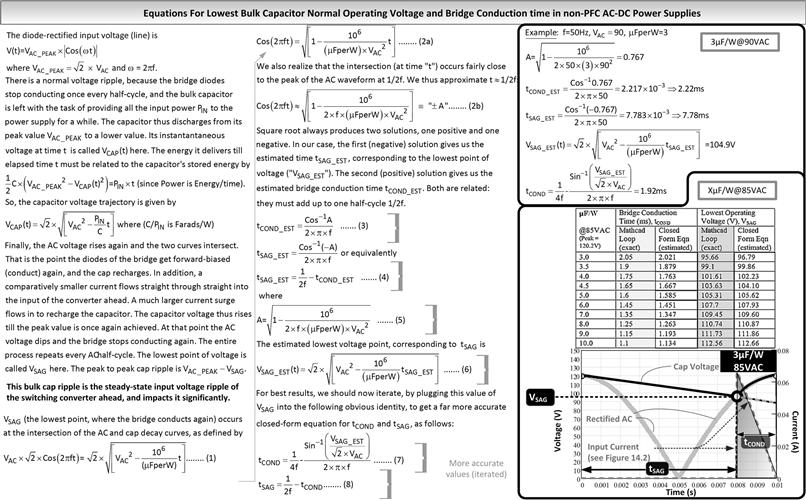
Figure 14.1: Calculating the conduction time and lowest voltage in steady operation.
The appropriate diodes of the bridge get forward-biased only when the magnitude of the instantaneous AC line voltage (the anode side of the bridge) exceeds the bulk capacitor voltage (the cathode side of bridge). At that moment, the bridge conduction interval (let us call that “tCOND” here) commences. Fast-forwarding a bit, a few milliseconds later, the AC line voltage starts its natural sine-wave descent once again. As soon as it dips, the anode-side voltage (line input) becomes less than the cathode-side voltage (the bulk capacitor). So, at that precise moment, the diodes of the bridge get reverse-biased and the conduction time interval tCOND ends. After tCOND, we enter what we are figuratively calling the “lean season” or “winter” here, the reason for which will become obvious soon. Note that since the repetition rate in our case is twice the line frequency, calling the line frequency “f” (50 Hz or 60 Hz), we see that the lean season lasts for exactly (1/2f) – tCOND, because it is basically just the rest of the time period till tCOND occurs again.
During this lean season, no “external help” can arrive – the diodes have literally cut off all incoming energy supplies from the AC source. The bulk capacitor therefore has to necessarily provide 100% of the power/energy requirement being constantly demanded by the switching converter section. In effect, the capacitor takes on the role of a giant reservoir of energy, and that is the main reason for its presence and size. This lean season is therefore often referred to as the “discharge interval” (of the cap), whereas tCOND is often called the “charging interval”.
After the conclusion of this “lean season”, the bridge conducts once again (when the AC voltage rises). So, tCOND starts all over again. But, connecting the dots, we now realize that by the required energy balance in steady state, the energy pulled in through the bridge during tCOND must not only provide all the instantaneous input energy being constantly demanded by the switching converter stage, but also completely replenish the energy of the bulk cap – i.e. to “restock” it, so to say, for the next lean season (when the bridge stops conducting again).
In terms of the widths of the two intervals involved: the diodes typically conduct for a much smaller duration than the duration for which they do not conduct. We can visualize that this ratio will get even worse for larger and larger bulk capacitances. The reason for that is that since the voltage across a very large cap will decay only slightly below its max value (relatively speaking), and since its max value is equal to the peak AC voltage, the diodes will get forward biased for only extremely short durations, very close to the peak of the AC input voltage waveform (see Figure 14.1). In such cases, we realize that since all the energy pulled out of the bulk cap during the “lean season” must be replenished in a comparatively smaller available time tCOND, the energy/current inrush spike during tCOND will necessarily be both very thin and very tall – since the area under the input current/energy curve must remain almost constant.
Increasing the Capacitance, Thereby Reducing tCOND, Causes High RMS Currents
We present a useful analogy here that we are calling the “Arctic analogy”. Consider situation where we have to provide winter food supplies for 10 scientists stationed in an Arctic camp. Suppose each scientist consumes 30 kg of food per month. So together, they need 300 kg of food per month. In the first possibility, suppose the summer is 2 months long. Also assume that summer is the only time we can transport food into the camp. So during those two summer months we need to send (a) winter supplies for 10 months (10×300=3000 kg), and (b) food for the two ongoing summer months (2×300=600 kg). That is a total of 3600 kg (a year’s supply as expected), delivered over 2 months, i.e. at the rate of 1800 kg per month on an average. In the second case, suppose summer was just 1 month long. Calculating similarly, we realize we now need to deliver a year’s supply in just 1 month, i.e. at the rate of 3600 kg per month on average.
That is what happens in a low-power AC–DC power supply too. During tCOND (summer), energy (food) is pulled in from the input source (supermarkets). During this period, the inputted energy goes not only into sustaining the PWM section (the scientists), but also recharging the bulk cap (the Arctic warehouse). During the lean season (winter), all the energy (food) required to sustain the PWM section comes only from the bulk capacitor. And so, very similarly, if we reduce tCOND (the summer months) by half, the current/energy amplitude (the food transported per month) will double.
But why is that a problem? The problem is that though the average value of current does not change if we halve tCOND, (check: IAVG=I×D=2I×D/2), the RMS value of the current goes up by a factor ~1.4. Check: I×√D ≠ 2I×√(D/2)=√2×I×√D=1.4×I×√D. Generalizing, if we reduce tCOND by the factor “x”, the RMS of the input current will increase by approximately the factor √x. Alternatively stated, the RMS of the input current must vary as 1/√tCOND. We can check this relationship out: if tCOND halves, the RMS input current will increase by the factor √2 as expected. Further, we can say that the peak current is roughly proportional to 1/tCOND. We can check this out too: if tCOND halves, the peak input current will increase by the factor 2 as expected.
Be clear that so far we are only referring to the current flowing in through the input filter chokes (the diode bridge current). We are not talking about the capacitor current, though that is very closely related to the bridge current as described in detail later, in Figure 14.2.

Figure 14.2: The peak/RMS current stresses in the capacitor, bridge and EMI filters.
We know that the heating in any resistive element depends on IRMS2. So now it becomes clear why the filter chokes start to get almost “mysteriously hot” if the bulk capacitor is made injudiciously large causing tCOND to reduce as a result. The reason is the RMS has become much higher now.
We also know that if tCOND halves, the peak current doubles. But we know from Chapter 5 that the saturation current rating (and size) of any magnetic component depends on IPEAK2. So we conclude that if tCOND halves, the size of the filter choke will quadruple. And if we didn’t expect that or plan for it upfront, we can be quite sure our filter choke will start saturating, reducing its efficacy significantly.
Note: In Chapters 15 to 18 we will learn that common mode filter chokes have equal and opposite currents through the coupled windings, so core saturation is not actually a major concern for them, though heating certainly is. However, for differential mode chokes, both saturation and heating are of great concern. So in general, the input peak and RMS current must both be contained, by not selecting an excessively large bulk cap.
We are seeing a familiar trend: a peaky input energy/current shape causing huge RMS/peak stresses that can dramatically affect the cost and physical sizes of related components. In general, we should always remember that “a little ripple (both voltage and current) is usually a good thing” in switchers and we shouldn’t be “ripple-phobic”. We had received the same lesson in Chapters 2 and 5 when we decided to keep the current ripple ratio r at an optimum of around 0.4 (±20%) rather than trying to increase the inductance injudiciously to lower r. But, eventually, we must keep in mind it is all about design compromises. For example, in the case under discussion here, reducing the bulk cap injudiciously can have also led to adverse effects. For example, it can cause the PWM switch dissipation to increase significantly, besides requiring its transformer to be bigger. In other words, there is no clear answer – it is just optimization as usual.
The Capacitor Voltage Trajectory and the Basic Intervals
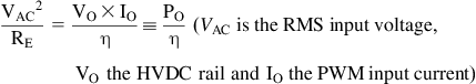
We are interested in computing the cap voltage as a function of time as it discharges (decays) during tCOND (as we continue to pull energy out of it). There are many possibilities in the way we can discharge a capacitor and the corresponding voltage trajectory it takes. For example, if we connect a resistance to the capacitor, it will discharge as per the familiar exponential-based capacitor discharge curve (~e−t/RC) discussed in Chapter 1. Suppose we were to attach a constant current source “I” across the bulk capacitor. Then its voltage would fall in a straight line as per the equation ΔV/Δt=I/C. However, in our case here, we are connecting a switching converter across the cap. Its basic equation is PIN=VO×IO/η, where η is the efficiency (the input power of the converter is the power being pulled out of the capacitor). This power is clearly independent of the input voltage (assuming the efficiency η is almost constant). In other words, PIN is virtually constant irrespective of the capacitor voltage. So, the switching converter presents itself to the cap, not as a constant resistance or constant current load, but as a constant power load, which means the product “VI” is constant as the cap decays. The corresponding trajectory can be plotted out with this mathematical constraint, as shown in Figure 14.1.
In Figure 14.1 we try to find the corresponding diode conduction time tCOND and the corresponding lowest capacitor voltage VSAG. The required math and the underlying logic are presented therein. The basis of these computations is as follows: we are trying to find the intersection of two distinct curves, the rectified sine-wave AC input and the capacitor discharge curve.
In the process of deriving the closed-form (estimated) equations we have needed to make an initial assumption: that the instant at which the intersection (lowest voltage) occurs (t=tSAG) is situated just before the instant at which the AC voltage reaches its peak (t=1/2f). However, we then iterate and get very accurate estimates from the closed form equations. To prove the point, within Figure 14.1, we have also gone and compared the closed-form estimates with the more accurate numerical results obtained from a very detailed iterative Mathcad file, one that did not make the above simplifying assumption. We see from the embedded table in Figure 14.1 that the comparison is very good indeed (after the iteration). We conclude it is OK to use the closed-form equations (judiciously). In Figure 14.1 we have also included a numerical example to calculate tCOND, tSAG and VSAG, the three key terms of interest here.
The reader will observe that we are ultimately trying to scale everything to Capacitance per Watt (usually called “μFperW” or “μF/W”). The advantage of doing that is the curves and numbers become normalized in effect. So, by scaling the capacitance proportionally to the (input) wattage, we can then apply the results to any power level. There will be worked examples shortly, to illustrate this procedure.
Note: Look hard at the plot in Figure 14.1 to understand why an error in the estimated tSAG will not create a big error in VSAG, provided we plug the first-estimate tSAG into in the capacitor discharge curve, not in the AC curve.
Note: We are consistently ignoring the two forward diode drops that come in series with the input source during tCOND – an assumption that can affect the calculated VSAG by a couple of volts. However that is still well within component and other tolerances, so it is fair to ignore it here in the interest of simplicity.
Tolerating High Input Voltage Ripple in AC–DC Switching Converters
The bulk capacitor voltage ripple can be expressed as ±(VAC_PEAK−VSAG)/2×100%. For example, from Figure 14.1, we see that at 85VAC and for 3μF/W, the cap voltage will vary from a peak of 120 V (i.e. 85×√2) to about 96 V. The average is therefore (120+96)/2=108 V. That constitutes a voltage ripple of 24 V/108 V=0.2, i.e. 22%, or ±11%.
We realize that the input ripple to the high-voltage switching converter stage is no longer within the usually declared “rule” of <±1% input voltage ripple, for selecting the input capacitance of a typical low-power DC–DC converter. In fact, in commercial AC–DC applications, an input voltage ripple of up to around ±15% may be considered normal, or at least acceptable/permissible, if not desirable.
As indicated previously, for several reasons, using a huge bulk capacitance, just to smoothen out the voltage ripple, is really not a commercially viable option and nor does it help improve overall system performance. So it is actually preferable that we learn to tolerate, if not welcome, this rather high input ripple – by using workarounds to the problems it can cause. For example, we know that at least the controller IC certainly needs much better input filtering, or it can “misbehave”. The recommended solution to that problem is to add a small low-power, low-pass RC circuit just before the supply pin of the controller IC. That brings the input ripple as seen by the IC down to a more acceptable level (around ±1%). The high voltage ripple of around ±10% is then only “felt” only by the power stages, and that is deemed acceptable.
We realize that some of the ripple present on the input power rail gets through to the output power rail of any converter too. That aspect was discussed in Chapter 12. To combat this effect, an LC “post filter” (perhaps just using a cheap rod inductor followed by a medium-sized capacitor) can be added to the output of the converter.
However, eventually, it is undeniable that the input voltage ripple applied to the converter (power) section is rather large, and does affect the converter’s design and overall performance (also of its input EMI filter). To re-iterate, there is no right answer to what the “correct” amount of ripple is – it is based on optimization and careful design compromises.
How the Bulk Capacitor Voltage Ripple Impacts the Switching Converter Design
We realize that the peak voltage applied to the switching converter is fixed – it is simply the (rectified) peak of the AC line voltage. Therefore the amount of input ripple we allow, indirectly determines two other important parameters: (a) the lowest instantaneous input voltage VSAG, and (b) the average input voltage applied to the converter. Why are these important? We take up the latter first.
(A) As voltage at the input of the converter (bulk capacitor voltage) undulates, so does its duty cycle as the converter attempts to correct the varying input and create a steady output voltage. We know that in a flyback topology for example, as we lower the input voltage, the input current (and its center of ramp IOR/(1 – D)) goes up on account of the increase in D at low input voltages. So the RMS current in the switch will go up significantly on account of higher input voltage ripple. Since the input voltage is undulating between two levels (VAC_PEAK and VSAG), the normally accepted assumption is to take the average value of the input voltage ripple, VIN_AVG, as the input voltage applied to the switching converter. This is OK for the purpose of calculating the (average) duty cycle and thereby the (average) switch dissipation and so on. Efficiency estimates can also be done using this average input voltage.
![]()
For example, in a typical universal input flyback (3μF/W @ 85VAC), the average input voltage is typically 108 V as mentioned above (often taken to be 105 V to account for the bridge diode drops too).
(B) The amount of ripple also determines VSAG. We need to ensure that the switching converter’s transformer does not saturate at VSAG. In other words, using an average voltage for deciding transformer/inductor size is a mistake. Magnetic components can saturate over the course of just one high-frequency cycle, leave aside a low-frequency AC cycle. And if that happens, immediate switch destruction can follow. Therefore, the core size selection procedure for a flyback, as presented in Chapter 5, should actually be done at least as low as VSAG. Even better, we should do the design typically about 10–20% lower than VSAG – or till the point of the set undervoltage lockout and/or max duty cycle limiting and/or current limiting.
Note: Any calculations related to required copper thickness, and any other heat-related components, can be selected using the average voltage VIN_AVG given above since heat is determined on a continuous (averaged) basis. For example, the switching transformer size is determined by VSAG, but its thermal design (wire gauge and so on) is determined by VIN_AVG.
General Flyback Fault Protection Schemes
This is a good time to discuss flyback protection issues briefly. We indicated above that a flyback power supply can easily blow up at power-up or power-down because of momentary core saturation. This was discussed briefly in Chapter 3 too. It is just not enough to design the transformer “thinking” that the lowest input voltage is going to be VSAG. Because in reality, the input of the flyback does go down all the way to zero during every single power-down.
The strategy to deal with the ensuing stress is as follows. We first need to know what the value of VSAG is (during normal operation). Because that represents an operating level we do not want to affect, or inadvertently “protect” against. Thereafter, we must place an accurate undervoltage lockout (UVLO) and/or a corresponding switch current limit just a little below VSAG. Note that if the current limit is set too high (commensurate with a much lower input voltage), we can suffer from the dangers of core saturation on power-up and power-down if the core has been designed only for VSAG, or just a little lower. On the other hand, if the current limit is set too low, corresponding to a higher minimum input operating voltage, and/or the UVLO level is set too high, we start to encroach into the region of normal operation, which is obviously unacceptable.
The underlying philosophy of protection is always as follows: any protection barrier must be built around normal operation and just a little wider. Note that if the power supply has also to meet certain holdup requirements (to be discussed shortly), the protection will usually have to be set at even a lower voltage, or the bulk capacitor and/or core will need to be significantly oversized.
Note: One common misconception is that carefully controlling the maximum duty cycle is all that is required to protect a flyback during power-up and power-down. It does help, and certainly, it should be set fairly accurately too. However, it is not enough by itself. Because, duty cycle is rather loosely connected to the DC level of current in CCM, as has been explained several times in previous chapters. So we also need current limiting and undervoltage lockout (UVLO) protection.
Note: Typically, the normal operating duty cycle for an AC–DC flyback operating at its lowest rated AC input voltage (e.g. 85VAC) is set to about 50–60%, as discussed in Chapter 3 (see worked example 7 in particular). Therefore, a maximum duty cycle limit (Dmax) of about 60–65% is usually set for ensuring reliability under power-up and power-down. It is not considered wise to use a controller IC with any arbitrary Dmax. For example, there are some integrated AC–DC Flyback switchers that are built around what is to us at least, an inexplicable and arbitrary “78% max duty cycle limit” (e.g. Topswitch-FX and GX). Another mystifying example is the LM3478, a flyback switcher IC with a “100% max duty cycle” (perhaps the only one such IC in existence, because normally, 100% max duty cycle is acceptable, and even desirable, for Buck ICs, but never for Boost or Buck-Boost topologies).
We must mention what happens at high input voltages. At that input point, a universal input power supply (90–270VAC), will have a rectified peak DC of 270×√2=382 V. Even if the flyback has a good zener/RCD clamp to protect itself from voltage overstress at this input, it can still be destroyed merely by an inadvertent current overstress. But how can that happen at high voltages? Let us do some simple math here. To keep the equations looking simple, we simply designate VMIN and VMAX as the minimum and maximum input voltages going to the switching converter (i.e. the minimum and maximum cap voltages) respectively. Their corresponding duty cycles are designated DMAX and DMIN. Note that here DMAX is not the max duty cycle limit of the controller IC but the duty cycle at the lowest operating input voltage. For a flyback we thus get
![]()
Eliminating VO (or equivalently VOR)
![]()
So,
![]()
Note that we can divide both the numerator and denominator above by √2 and it would still be valid. So, we can just directly plug in the AC voltages in the equation above. For example, if we had designed the flyback with a DMAX of 0.5 (ignoring ripple in this particular discussion), the operating duty cycle at 270VAC would be
![]()
We had stated that it is always desirable any protection barrier be just a little wider than normal operation. So, the obvious problem we can foresee here is related to the fact that we have set the max duty cycle (protection level) at 65% for the purpose of catering to low input voltages (along with the rather stressful power-up and power-down scenario discussed above). However, now we also realize that the 65% duty cycle limit is too wide for protection of the flyback at 270VAC operation, because at 270VAC the normal operating duty cycle is only about 25%. It is in fact true that we can easily destroy any such poorly designed AC–DC flyback power supply by simply inducing core saturation at high input voltages. All we need to do is create a sudden overload at 270VAC, and the control loop will naturally react by pushing out the duty cycle momentarily to its maximum (65% in this case) in an effort to regulate the output. In going from 90VAC to 270VAC, the applied voltage across the transformer goes up three times. Therefore, in addition to that problem, if the time for which that high voltage gets applied to the transformer remains the same it was at low voltages, we have a major problem in the form of three times (300%) the voltseconds under sudden overloads at high line as compared to sudden overloads at low line. We also know that magnetic components can easily saturate purely due to excess applied voltseconds. For example, in our case here, even though the center of the inductor ramp has come down by a factor of two at high line (remember, the center of ramp varies as per 1 – D), the increased AC current swing riding on top of it, due to the excessive applied voltseconds described above, can cause the peak instantaneous current under overloads at 270VAC to significantly exceed even the worst-case peak currents observed at 90VAC. So, this situation can cause easily transformer core saturation, and in fact, far more readily than possible at low line.
So, how do we guard against this high-line overload scenario? The easy way to close this particular vulnerability of the flyback/Buck-Boost/Boost topologies, is called ‘Line Feedforward’. In many low-cost flyback power supplies using the popular UC3842 IC for example, a large additional resistor of around 470 k to 1 M is almost invariably found connected from the rectified high voltage DC line (HVDC rail) to the current sense pin (on the IC side). That way, a voltage dependent current gets summed up with the normal sensed current coming in through the typical 1 k or 2 k resistor connected to the sense resistor placed in the Source lead of the switching FET. In effect, the additional high-value resistor raises the sensed current pedestal (its DC value) higher and higher as the input voltage is raised. So, the current limit threshold of the IC is reached much more readily at high line, even for much smaller switch currents. We can say that, in effect, the max duty cycle has gotten limited at high line, to just a little more than required for normal operation. This input/line feedforward technique therefore provides necessary protection under the overload scenario described above, provided the high-value resistance mentioned above is rather carefully set.
The Input Current Shape and the Capacitor Current
In Figure 14.1, we had shown a triangular-shaped current waveform to represent the input (bridge) current. Theoretically, that is the correct shape as can be seen from the detailed derivation in Figure 14.2. In reality, because of input/line impedances along the way, the actual observed input current (bridge) waveform is perhaps closer to a triangle with rather severely rounded edges. Note that it is certainly not a rectangular current waveshape, as often simplistically assumed in literature (e.g. older Unitrode Application notes). The predictions of peak and RMS currents based on the theoretical triangular waveshape, as derived in Figure 14.2, are accurate, if not a little pessimistic (since they ignore line impedances), but they certainly can, and should, be used for doing a worst-case design.
In general, the bulk capacitor current waveform can be derived from the bridge current by subtracting the DC value IIN from the bridge current as per the procedure shown in Figure 7.5 and Figure 7.6. Alternatively, the diode current is simply the capacitor discharging current with IIN added to it as indicated in Figure 14.2.
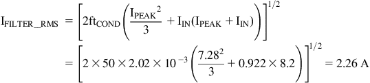
In Figure 14.2, we have also provided some quick lookup numbers in gray for the most basic low-cost case of 3μF/W @ 85VAC. An embedded example in the figure shows how to use these quick lookup numbers to quickly scale and estimate the peak currents and also the capacitor ripple current, for any application. For example, we have shown that a power supply drawing 30 W at its input, and using 90μF of bulk capacitance (i.e. 3μF/W), has a peak diode current of 2.43A at 85VAC. This is based on the quick lookup number of 0.081A/W provided for the case of 3 μF/W @ 85VAC.
In Table 14.1, we have consolidated all the required equations and also provided quick look-up numbers for several μF/W cases (including 3 μF/W). This table is perhaps all we need for designing a low-power AC–DC front end. However, there are certain “holdup time” and capacitor tolerance considerations that we will discuss soon, which could affect our final choice of μF/W and also the switcher’s transformer design.
Table 14.1. Design Equations and Quick Lookup Numbers for Low-Power Front-End Design.
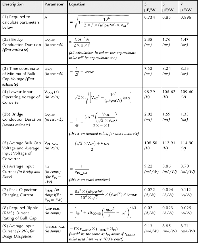
Notes: Calculations are meant to be done from top to bottom, in that order.All A/W and μF/W numbers are normalized to PIN=1W.All numbers are for 85VAC and Line Frequency f=50 Hz.
Further, there is actually a much simpler and intuitive way to estimate several stress parameters, based on the “Arctic winter analogy” we had presented in a preceding section. We will look at that shortly.
How to Interpret μF/W correctly
Some semiconductor vendors, intending to showcase their small evaluation boards to demonstrate how “tiny” their integrated flyback switchers are, often calculate the input capacitance based on a supposedly “universal rule of 3 μF/W”. Though we do have some reservations about this number itself as discussed later, the way these vendors apparently choose to interpret this number makes their recommendations really questionable.
These vendors apply the “3 μF/W rule” to the output wattage, not the input wattage. That is not consistent. Keep in mind that the input bulk capacitor is handling output power plus the loss. So the input cap really doesn’t care about the output power per se, only the input power. In other words, a 3 μF/W rule, if considered acceptable, should be applied to the bulk cap based on input watts, not output watts. Otherwise we will end up with contradictory design advice.
Note: For example, if there is a 50 W power supply with 80% efficiency, this vendor would recommend an input capacitor of 50×3=150 μF (nominal). But then, along comes another 50 W power supply, this time running at say, only 50% efficiency (to exaggerate the point). The vendor would however still recommend 150 μF. However, with these recommendations in place, we will find that the two power supplies will have very different input capacitor waveforms and very different tCOND, tSAG and VSAG. So they must be different cases now, even though the vendor seemed to say the two power supplies would behave similarly with their recommendations. However, had we instead kept the capacitances per input watts of the two supplies the same, we would have arrived at exactly the same tCOND, tSAG and VSAG for both cases. And so, to get the same (normalized) waveform shapes, we need to actually use 62.5 W×3 μF/W=187.5 μF in the first case, and 100 W×3 μF/W=300 μF in the second case (assuming we are willing to accept 3 μF/W in the first place).
Worked Example using either Quick Lookup Numbers or the “Arctic Analogy”
Example
We are designing an 85 W flyback with an estimated efficiency of 85%, for the universal input range of 85 to 270VAC. Select an input bulk cap tentatively, and estimate the key current stresses.
The Input power is 85 W/0.85=100 W. Let us tentatively select a 300 μF/400 V capacitor. We have thus set CBULK/PIN=300 μF/100 W=3 μF/W. We can work out the key stresses (@ worst-case 85VAC) in two ways.
Method 1: Let us use the quick lookup numbers presented in Table 14.1 for the 3 μF/W case here.
(a) tCOND=2.02 ms, from Row 2b.
(c) Average Cap voltage is 108.5 V, from Row 5.
(d) Average Input Current (and average bridge current) is 9.22 mA/W×100 W=922 mA, from Row 6.
Note: Bridge dissipation is about 2×1.1 V×0.922 A=2.0 W (assuming each diode has a forward drop of 1.1 V as per datasheet of bridge). We have used the exact value of average line current here, one that is unaffected by error in tCOND estimate. Since average capacitor voltage is 108.5 V, we get input power as 108.5×0.922=100 W as expected.
(e) Capacitor RMS current (predominantly a low-frequency component, to correctly pick capacitor ripple rating) is 0.02×100=2.0 A, from Row 8.
(f) RMS Input Current (to correctly pick AWG of all input filters) is 0.022×100=2.2 A, from Row 10.
(g) Peak Input Current (to rule out differential-mode input filter saturation) is 0.081×100=8.1 A, from Row 11.
Method 2: Here, we need the logic of the Arctic analogy presented earlier. We do need the closed-form equations of Figure 14.1 to estimate tCOND and VSAG. We also refer to some of the geometric RMS equations in Table 14.1 (based on Figure 7.4).
(a) tCOND=2.02 ms, from the table or equations in Figure 14.1.
(b) VSAG=96.8 V, from the table or equations in Figure 14.1.
(c) Average Cap voltage is therefore (85×√2 + 96.8)/2=108.5 V.
(d) Average Input Current (and average bridge current) is IIN=100 W/108.5 V=922 mA. We are using the terminology shown in the plot inside Figure 14.2.
(e) Now, using the Arctic analogy, we have to provide
εIN=PIN×t=100 W×10 ms=1000 mJ=1 J every half-cycle. This is analogous to one year’s food supply and we have to supply all of this in tCOND=2.02 ms (summer). Since by definition, ε=V×I×t, the average supply current during tCOND must therefore be I=ε/Vt → 1 J/(108.5×2.02 ms)=4.56 A. The average input current throughout the half-cycle is 0.922 A from above. This is the pedestal on top of which is the triangular portion of the input current (see Figure 14.2). The average of all this must equal 4.567 A. So, we get the peak input current (into cap) as
![]()
(f) The peak input current (through filter and bridge) is the peak cap current plus IIN which is going to the switcher section, as shown in the plot in Figure 14.2. So the peak input current is 7.28 A + 0.922=8.2 A. This agrees very well indeed with the estimate of peak input current in step (g) of Method 1 above.
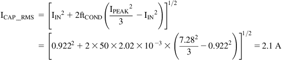
This agrees very well indeed with the estimate of cap RMS current in step (e) of Method 1 above.
(h) The input filter RMS current is
This agrees very well indeed with the estimate of cap RMS current in step (f) of Method 1 above.
We now realize that armed primarily only with the Arctic analogy, we could get through all the stress estimates accurately, without resorting to complicated equations. Further, we are no longer tied to any specific values of μF/W. We could have chosen any capacitance at all to proceed. This illustrates the sheer power of understanding basic principles, rather than just leaning on cumbersome math and simulations. Further, we see that carefully selected intuitive analogies like the Arctic analogy do a lot to bolster basic understanding.
Accounting for Capacitor Tolerances and Life
A typical aluminum electrolytic cap may have a nominal tolerance of ±20%. In addition, we have to account for its end-of-life capacitance, which could be 20% lower than its starting value. If we do not account for these cumulative variations upfront, we run the risk sooner or later, of encountering a much lower VSAG than we had expected or planned for, and also a much lower holdup time (as discussed further below). Therefore a thorough design will calculate a certain minimum capacitance, say “X” μF, but then use an actual nominal capacitance 56% higher, i.e. 1.56×X μF (check: 1.56×0.8×0.8=1).
For example, a 30 W universal input power supply running at 90% efficiency has an input power of 30/0.9=33.3 W. Using the 3 μF/W rule, we get 33.33×3=100 μF. But this is just the minimum capacitance we need to guarantee here. The capacitor we should actually use must be at least 156 μF nominal. Therefore, we will go out and pick a standard cap value of 180 μF (nominal). The required voltage rating of the cap is obviously 265VAC×√2 → 400 V since it has to handle the highest voltage across it.
But all this introduces another complication. We now actually need to split our front-end design phase into two distinct design steps at this point – we certainly can’t base any of our estimates on the starting value of 100 μF anymore.
Step 1: We realize that the initial capacitance can actually be 20% higher on account of tolerances, i.e. CMAX=1.2×180 μF=216 μF. A high capacitance leads to a much smaller worst-case tCOND, which in turn leads to much higher peak and RMS currents in both the input filter chokes and the RMS current through the bulk cap. So, to correctly pick the ripple current rating of the input cap, the wire gauge of the input filter chokes and also the saturation rating of the differential mode input chokes, we must now consider the lowest possible tCOND as calculated above – based on CMAX=216 μF. That corresponds to a maximum μF/W of 216/33.33=6.5 μF/W. Looking at Figure 14.1 we see we can easily interpolate between the Mathcad values for 6 and 7 μF/W to get tCOND=1.4 ms and VSAG=108.6 V. These are all we need to work out the stresses using the Arctic analogy! Or we can use the more detailed equations in Table 14.1.
Step 2: On the other hand, to find the worst-case “hold-up time” (explained further below), the worst-case dissipation in the switch and the appropriate wire gauge selection and resulting dissipation of the switching transformer, we should use the maximum tCOND (based on lowest capacitance). The lowest capacitance value the selected bulk capacitor can exhibit over its useful life is CMIN=180 μF×0.8×0.8=115 μF. That is a minimum μF/W of 115/33.33=3.45 μF/W. This is the value we need to use for this step of the design. Basically, on this basis, we need to work out the maximum tCOND and the lowest VSAG during normal operation (over the life of the product). Then we find out the lowest average input to the switching converter (VIN_AVG) and use that voltage for finding the average duty cycle and corresponding RMS stresses in the switching converter stage in the usual fashion, as discussed in Chapter 7. Then we need to look at the holdup time charts provided below, to work out the lowest cap voltage during an input dropout event so we can correctly size the flyback transformer.
Note that in both cases above, we usually do not need to perform any of the stress/dissipation calculations at high line, because the worst case currents are at low line (for a flyback). Also, faced with a possibility of either 50 Hz or 60 Hz line input frequency, we note that 50 Hz gives the worst case results. So we are mostly ignoring the 60 Hz case in this chapter.
Holdup Time Considerations
Holdup time is the duration for which the output of the power supply/converter stays within regulation on loss of input power. The intent is simple: incoming power quality (e.g. AC mains) is not always clean and/or assured. So, to avoid frequent nuisance interruptions, we try to provide a small, but guaranteed duration, for which the input power can go away, or just sag below the declared input specifications of the power supply/converter, and then come back up, without the load/system connected to the output of the converter from ever “knowing” that something transpired at the input of the supply/converter. In the process, the output of the supply/converter may droop by a very small but almost unnoticeable amount (typically <5% below nominal or within the declared output regulation range of the supply). Holdup time is therefore a buffer against ever-present vagaries in input supply quality.
Note that if the input voltage is really collapsing (as in an outage), holdup time may be used to keep things alive for just a while, deliver some sort of flag or advance warning of the impending outage, and thereby provide a few milliseconds for the load/system to perform any necessary housekeeping. For example, the system may store the current state, configuration or preferences, or even a data file currently in use, so as to recover or recall them quickly when power returns.
Though the underlying concept and intent of holdup time is always the same as described above, its measurement, testing and implementation need to be treated quite differently when dealing with DC–DC converters, PFC-based AC–DC power supplies or non-PFC-based AC–DC power supplies, the latter being the topic of discussion here. Some make the mistake of trying to apply textbook equations meant for achieving a certain holdup in DC–DC converters, to AC–DC power supplies. There are major differences in all possible implementations as explained below.
Consider the case of an AC–DC power supply providing, say 12 V output, which then goes to a point-of-load (POL) DC–DC converter that then converts the 12 V to 5 V. On the 5 V rail is our load/system that we need to keep alive by guaranteeing a certain holdup time. In principle, we can try to meet the required holdup time in a variety of ways.
(a) We can simply try to increase the output cap of the POL converter in a brute-force fashion, so as to reduce the output droop. Let us test this out. Suppose the POL converter is a 12 V to 5 V Buck converter delivering 3 A with 80% efficiency. With a typical 5% allowed output droop, the lowest output voltage would be 5×0.95=4.75 V. Using the equation for a capacitor discharging, and targeting a modest holdup time of 10 ms, we get the corresponding capacitor requirement.
![]()
![]()
No typo here, that really is 123 000 μF! Obviously a very impractical value.
(b) Let us try to beef up the input capacitor of the POL converter instead. Suppose we imagine for a moment that the input source to the POL converter just “went away” briefly, leaving the input capacitor of the POL converter the task of providing all the necessary power requirement. We also assume this Buck converter has a certain switch forward drop and a maximum duty cycle limit, due to which it needs a certain guaranteed “minimum headroom” of say 2.5 V above the output rail, to be able to regulate. In effect, we are allowing the POL converter’s input capacitor voltage to droop from 12 V to 7.5 V, and we then expect that the output will stay regulated during this decay. However, remember that the input cap of this DC–DC stage has to handle the input power, not the output power. So the correct equation to use here is
![]()
![]()
This is about 30 times better than trying to meet holdup time directly at the output, but still way too high.
Note: The perceptive reader will notice that there can be problems with our assumptions above. In the first case, we tried to add capacitance to the output of the switching converter, imagining it would do something to prop up the output under all cases. However, if the input rail of the POL converter is being driven by, say, a synchronous output stage of the AC–DC supply, that stage can source or sink current. It can thus forcibly drive the input rail of the POL converter down to zero during an AC/line dropout. In that case, the output cap of the POL converter will also get forcibly discharged to zero through the body-diode of the switching FET of the POL converter, rendering it incapable of providing any holdup time. For the same reason, if we try to beef up the input cap of the POL converter, we could still be in trouble. The solution in such cases is to place a diode in series with the input of the POL converter – so, even if the output rail of the AC–DC stage gets pulled down to zero, the series diode would then get reverse-biased and prevent the input rail of the POL converter from being dragged to zero.
(c) Since the amount of capacitance required is still too high, we realize we need to move further “up the food-chain” if we want to provide holdup time of the order of several milliseconds in a practical manner. We finally reach the input side of the AC–DC power supply. We discover that that leads to far more acceptable capacitance values. Why? Because to achieve a certain holdup time tholdup, we basically have to provide a reservoir able to store and provide a certain fixed amount of energy equal to PIN × tholdup. But we also know that the energy storage capability of a capacitor goes as C×V2. So as we increase V, we get a dramatic increase in energy storage capability, even with smaller C. That is why any holdup time requirement is best met upstream – preferably on the input side of the AC–DC power supply – i.e. at its front end.
Let us understand why the AC input voltage source sags or drops out in the first place, and what its implications are. Most input disturbances originate locally. For example a large load may suddenly start up nearby, like a motor or a resistive/incandescent load. That can draw a huge initial current, causing a voltage dip in its vicinity. We could also have unspecified wiring flaws, or local faults/shorts, which will eventually activate a circuit-breaker, but will produce momentary dips in the line voltage till that happens. Some relatively rare voltage sags/dropouts can originate in the utility’s electric power system. The most common of those are a natural outcome of faults on distant circuits, which are eventually segregated by self-resetting circuit breakers, but only after a certain unavoidable delay during which sags/droops result. Much less common are sags/dropouts related to distant voltage regulator failures. Utilities have automated systems to adjust voltage (typically using power factor correction capacitors, or tapped switching transformers), and these also can fail on rare occasions. All these can lead to temporary sags/dropouts.
To create a level of acceptable immunity from such events, the international standard IEC 61000-4-11 (Second Edition 2004), calls for a minimum holdup time of 10 ms. This is actually intended to correspond to one half cycle of 50 Hz line frequency. Most commercial power supply specifications call out for a holdup time of 20 ms, and that number is intended to correspond to one complete AC cycle (two half-cycles).
However, looking at the reasons listed above for line disturbances, we realize that in almost all cases, when the input power does resume, it remains “in sync” with the previous “good” AC half-cycles. In other words, we should try and visualize line dropout in terms of missing AC half-cycles, not in terms of any fixed time interval of, say, 10 ms or 20 ms, and so on. We will see that that line of thinking can lead to significant cost savings.
Looking more closely at Figure 14.1, we can visualize that the situation for compliance to a certain holdup time spec depends on when exactly the dropout is said to have commenced. For example, if the input source drops out just before the bridge conducts again (i.e. close to and just before tSAG), that would represent the worst-case. Because in that case we are starting off the dropout-related part of the capacitor decay from the lowest possible operating voltage point, and we will ultimately arrive at a much lower voltage at the end of the dropout time. In contrast, the best case occurs just after the capacitor has been fully peak-charged. The IEC standard does not require that we should test holdup time either in the worst-case condition, or in the best-case. It just recommends that any input voltage changes occur at zero crossings of the AC line voltage, though it also leaves the door open for testing at different “switching angles” if deemed necessary. There is also the question whether the input AC voltage should be set to 115VAC (nominal), or as a worst-case: 90VAC, or even 85VAC.
There are many OEMs that demand aggressive holdup testing of power supplies – by asking for the input to be set at 85VAC, and commencing the dropout just before VSAG. That does increase the bulk capacitor/transformer size/cost significantly. However, especially in such cases, it is valuable to try and convince the OEM to talk of holdup in terms of the number of half-cycles missed, not in terms of a fixed duration expressed in ms. In doing so, we can recoup some of the higher costs.
The curves in Figure 14.3 show the trajectory for different μF/W, computed from the Mathcad program alongside. We can see that for example, one full missing AC cycle (two half-cycles) is in reality a little less than 20 ms (by the amount tCOND). Note that what we have been calling VSAG so far is now designated VSAG0, since it corresponds to zero missing half-cycles, or “normal operation”. To account for dropouts, we now have VSAG1, VSAG2, VSAG3 and so on, corresponding to 1, 2 and 3 missing half-cycles, respectively. The numbers for VSAGx are presented in the lookup tables within Figure 14.3.
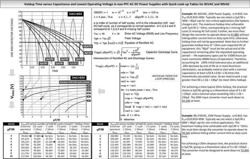
Figure 14.3: Holdup design chart based on missing half-cycles (not time).
Note that in Figure 14.3, we are establishing something close to 60VDC as the lowest acceptable point for flyback operation during a line dropout. So, looking at the curves and tables in Figure 14.3 we conclude that, based on an assumption of the most aggressive holdup testing:
(a) If the required holdup is one half-cycle (~10 ms), we can certainly use 3 μF/W, though we also should verify that the selected capacitor meets the ripple current requirement, so as to guarantee its life as per the procedure shown in Chapter 6.
(b) If the required holdup is two half-cycles (~20 ms), we must use at least 5 μF/W. Clearly, 3 μF/W is just not sufficient.
The above statements are based on the worst-case assumption of 85VAC input combined with a dropout commencing just before tSAG0 occurs. But, to enable the holdup time feature, we must also design the flyback such that it is able to deliver full power down to ~60VDC. For example, the protection circuitry we talked about must be moved out just past this lower operating limit.
Note: We do not have to size the copper of the transformer or use heatsinks for the switch/diode rated for continuous 60VDC operation, because we only need to deliver power at such a low voltage momentarily.
Note: A frequently asked question on capacitor selection is: what is the dominant criterion for selecting the HVDC bulk capacitor in non-PFC universal input AC-DC flybacks? The answer is as follows. Usually, with a 10–20 ms holdup time requirement, we may discover that we need to oversize the cap somewhat (getting higher capacitance as a bonus), simply because otherwise, its ripple current rating is inadequate. So here, it the RMS rating that ultimately dominates and determines the capacitor – its size and thereby its capacitance. But the holdup time spec is not far behind. So, for a holdup time of 30–40 ms, we will usually end up selecting a cap that automatically meets the required ripple current rating. In general, we can calculate and select a capacitor that meets the ripple current rating, and then separately calculate and select a capacitor that meets the required holdup time. Finally, we simply pick the larger of the two.
To allow a flyback to operate reliably down to 60VDC, the most important concern is to ensure that its transformer can handle the adverse stress situation gracefully (and without duty-cycle/undervoltage/current limit protections kicking in). Most universal input flybacks are designed to operate down to that low level, albeit momentarily. But it is also interesting to observe that commercial flyback transformer cores do not seem any bigger than what we may have intuitively expected on the basis of the worked examples and logic presented in Chapter 5. There are several reasons/strategies behind that. One “technique” comes from vendors of some integrated power supply ICs (e.g. Topswitch®). In their design tools they seem to “allow” designers to deliberately use a “peak BSAT” of ~4200 Gauss, which we know is far in excess of the usually declared 3000 Gauss max for ferrites (see Chapter 5). We do not bless that approach on these pages for that very reason. However, in the next section we present a design example that shows a legitimate way to stick to a max of 3000 Gauss, and yet keep the core size unchanged, while meeting the new holdup time requirements too. Of course, nothing comes for free, and there are some attached penalties as we will soon see.
Two Different Flyback Design Strategies for Meeting Holdup Requirements
Armed with all the detailed information on sags presented in Figure 14.3, we can do a much better job in designing a practical universal input AC–DC flyback. We go back to the design example we had initiated in Chapter 5, starting from Figure 5.19. In Figure 14.4 we show how to incorporate holdup time into those calculations. Our first step is to look at the right-hand side table of Figure 14.3 and pick a practical value of capacitance (e.g. 5 μF/W for meeting ~20 ms holdup time). We realize we now need to design the flyback such that it can function down to 73.5 V instead of the 127 V number we had used earlier. Note that we are relaxing our holdup spec just a bit, by demanding we comply with the holdup requirement at a minimum of 90VAC, not at 85VAC, which is why we have gotten 73.5VDC here instead of the earlier target value of ~60VDC.

Figure 14.4: Two practical flyback designs approaches for meeting holdup time requirements.
In fact, there are two possible design strategies as detailed in Figure 14.4, one that leads to a bigger core and one that doesn’t. Both are limited to a max BSAT of 3000 Gauss. The design approaches are otherwise quite different as described below.
(a) We can design the transformer for an r of 0.4 at 73.5 V, in which case the transformer will be no bigger than a transformer designed for r=0.4 at 127 V. We will explain the reason for that shortly.
(b) We can design the transformer for an r of 0.4 at 127 V, in which case, to be able to function reliably down to 73.5 V, we would need to choose a bigger core.
In Figure 14.4, using the first approach, we proceed exactly as we did in Figure 5.19, but we design the flyback at 73.5 V instead of 127 V. To our possible initial surprise, the required energy handling capability of the core (and its size) remains the same as at 127 V. Note that we haven’t even had to play with the air gap. Why is that? And how do we reconcile these results with our repeated advice to design the flyback transformer at the lowest input voltage?
The answer to this puzzle takes us back to Figure 5.4. That tells us something very fundamental: that a flyback transformer (or a Buck-Boost inductor) is unique because it has to store all the energy that the power supply delivers, and no more (let us ignore losses for now). We showed the term Δε was directly related only to the power (via the equation Δε=PIN/f), with no direct dependence on the input voltage (or D), unlike the other topologies. Then we moved on to Figure 5.6 and showed that the peak energy handling requirement of the inductor/transformer was not just the change in stored energy per cycle Δε, but εPEAK. That relationship was
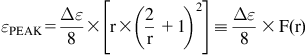
We should recognize that F(r) increases as r decreases.
We thus realize that for a flyback, since Δε does not depend on the input voltage it is r, and only r (besides of course the power rating of the converter), that determines εPEAK, and thereby the size of the core. So if we set r=0.4 at 73.5 V or r=0.4 at 127 V, and go no lower in cap voltage, the size of the core will be the same in both cases. However, if we set r to 0.4 at 127 V, and then a line dropout occurs, one that we wish to ride through via a holdup time specification, problems will arise. From Figure 2.4 we see that for a Buck-Boost, r decreases as the input voltage falls (D increases). In Figure 5.7 we had also explained that the term F(r) above rises steeply if r decreases far below 0.4. In other words, if we have chosen the inductance of the transformer such that r was set to 0.4 at 127 V and then a dropout occurs, the instantaneous r of the converter will decrease significantly, causing εPEAK to rise steeply. Therefore, if the core has not been sufficiently oversized to deal with this momentary stress situation, it will saturate. That is why in the two design approaches above, we will get differently sized cores.
In simple language this means, it is not necessary to increase the size of a flyback transformer, or even to change its air gap (z-factor) to meet any holdup requirements. We just need to reduce the number of turns and thereby reduce its inductance (higher r). Of course we do need to set correspondingly higher current limits, and so on.
As mentioned in Figure 14.4, the first approach does have problems. By setting r to 0.4 at such a low voltage of 73.5 V, as opposed to setting r to 0.4 at 127 V, the peaks current would increase much more at high line, and have higher RMS values too. Further, the system will go into DCM much more readily at light loads. In fact, even at the max rated load, it is most likely to be in DCM at high line. These are all the drawbacks of trying not to increase the size of the transformer while complying with the required holdup time specification. Nothing comes for free.
Finally, based on our preferences and design targets, we could decide which of the two above-mentioned transformer design approaches to pick. Better still, we may like to use a compromise solution. For example, we may want to set r=0.3 instead of 0.4 at 73.5 V. That will give a slightly bigger core, but better efficiency and performance at high line.
Part 2: High-Power Applications and PFC
Overview
Let us conduct a thought experiment. Suppose we apply an arbitrary voltage waveform (with a certain RMS value VRMS) across an infinitely large resistance. We know that the resistor stays “cold”, which indicates no energy is being lost inside it. Now suppose we pass an arbitrary current waveform (with a certain RMS value, IRMS) through a piece of very thick copper wire (assuming it has zero resistance). The wire still doesn’t get hot, indicating no dissipation occurs inside it (ignore dissipation elsewhere). To emulate these two operations, we now substitute a mechanical switch. One moment it is an infinite resistor (switch open), the next moment a perfect conductor (switch closed). Expectedly, the switch itself remains cold whatever we do and however we switch it (any pattern). We can never dissipate any heat inside an ideal switch. The perceptive reader will recognize this was the very basis of switching power conversion as explained in Chapter 1.
However, if we are a little misguided and put a scope across the mechanical switch we would see an arbitrary voltage waveform with a certain RMS value. Then, if we put a current probe in series with the switch, we would see an arbitrary current waveform with a certain RMS too. Then, suppose we do some “simple math” and multiply the RMS voltage across the switch (over a certain period of time) with the RMS current passing through it (over the same period of time). The product VRMS×IRMS would obviously be a large, non-zero number. But is that number equal to the power dissipated in the switch? Clearly no, since the switch is still cold. So what went wrong? In effect our “simple math” has misled us into thinking there was some dissipation in the switch. The “dissipation” we calculated above was not the real power, but the ‘Apparent Power’.
![]()
When dealing with AC power distribution, in which we use sine-wave alternating current (AC) voltages, this is equivalently written as
![]()
Note that “AC” is another name for “RMS”. For example, when we refer to the US household mains input as 120VAC, this is a sine wave with an RMS value of 120 V. Its peak value is 120 V×√2=170 V.
The real (or true) power is, by definition, the average power computed over a complete cycle
![]()
We actually ran into a similar potential discrepancy in the previous section where we had a worked example based on the ‘Arctic analogy’ though we did not point it out at that time. We recall we had shown that a 100 W (input power) converter with a 300 μF bulk cap, had an input RMS current of around 2.26 A (approximate). The apparent power was therefore, by definition, 85VAC×2.26 A=192 W. Whereas we know for a fact, that the real (or true) input power was only 100 W (108.5 V×0.922 A=100 W).
To document such situations, the term “power factor” was introduced. It is defined as the ratio of the real power to the apparent power. So in our example above, the power factor was 100/192 ~ 0.5. In principle, power factor can range from zero to unity, with unity being the best possible case. We should also have connected the dots by now, and realized that higher and higher bulk capacitances will only make things worse in a low-power AC–DC front end – by causing the power factor to decrease even further, thereby causing much higher heating in related components.
Note that above, we have already indicated the underlying problem with low power factor – that even though only the “apparent” power is said to have increased, the effect of this apparent power is very real in the sense that the dissipation in nearby components increases significantly.
There is a growing demand that AC–DC power supplies, besides other mains appliances, have high power factors. A key reason is higher associated equipment and transmission costs to utility companies. But first, let us take a deep breath by recognizing that common household electricity meters don’t charge us for “apparent power”, only for “real power”, or it is possible we would have acted with much greater personal haste in ensuring power factor correction (PFC) is implemented in all household appliances/power supplies. However, a low power factor does impact us directly, especially at higher power levels – by limiting the maximum RMS current we can pass through our household wiring, thus indirectly limiting the apparent power and also thereby the useful power we can get from it. Keep in mind, that if we have a “15A-rated” outlet, we are not allowed to exceed 15 A (RMS) even momentarily. Circuit breakers would likely go off to protect the building and stop us in our tracks.
Here is a specific numerical example to show the power limiting imposed by a low power factor. We are basing it on the standard 120 V/15 A outlet circuit commonly found in offices and homes in the US. In principle, this outlet should not be used to handle anything more than 120 V×15 A×0.8=1440 Watts of power. Note that we have introduced a derating factor of 0.8 above, thus effectively maintaining a 20% safety margin (which will also prevent nuisance tripping of any circuit breakers in the bargain). Note that the computed 1440 W max in effect refers to the maximum apparent power, not the real power, since heating in the wiring depends only on IAC (or IRMS), and therefore on the apparent power, not on the useful power going through the wire (at least not directly). So, assuming that the overall efficiency of our AC–DC power supply is 75%, the power supply can be rated for a maximum output power of 120 V×(15 A×0.80)×0.75=1080 Watts. That would correspond to exactly 1440 W at its input (check: 1080/0.75=1440). But this assumes the power factor was unity. If the power factor was say, only 0.5 for example, as is quite typical in simple bridge-plus-cap front ends, the maximum output power rating of our power supply can only be 120 V×(15 A×0.80)×0.75×0.5=540 Watts. Check: 540/(0.75×0.5)=1440 W. Further, in effect, we are also wasting the current-carrying capability of the AC outlet. Had we reduced the peak/RMS currents for a given output power, we could have raised the output power significantly. The best way to do that is to try and achieve a higher power factor.
In this chapter we are not going to go deep into concepts of reactive power versus real power and so on, other than to point out that a load consisting of a pure resistor (no capacitor or inductor present) dissipates all the energy sent its way, so its power factor is unity. The basic reason why we got a power factor of less than 1 in our low-power AC–DC front-end was very simply the input capacitor. And for the same reason, if we have a circuit consisting exclusively of pure inductors and/or pure capacitors (no resistors anywhere), the power factor will be zero. We can only store energy, never dissipate it, unless we have a resistor present somewhere. Because, though any L/C circuit would seem to initially take in energy from the AC source (judging by the observed overlap between the voltage and current), in a subsequent part of the AC cycle the relative signs between the voltage and current would flip, and at that moment, all the energy that was taken in (i.e. stored) would start being returned to the AC source. So the real (net) incoming power (computed as an average over the whole cycle) would be zero, but the apparent power would not. And the power factor would then be zero too.
We conclude that the way to introduce power factor correction in AC–DC power supplies is to make the power supply (with its load attached as usual) appear as a pure resistor to the AC source. That is our design target in implementing PFC.
What exactly is so special about a resistor’s behavior that we want to mimic? If we apply a sine-wave voltage waveform across a resistor, we get exactly a sine-wave current waveform through it. If we apply a triangular voltage waveform, we will get a triangular current waveform. A square voltage will produce a square current and so on. And there is no time delay (phase shift) in the process either. We conclude that at any point in any arbitrary applied waveform, the instantaneous voltage is always proportional to the instantaneous current. The proportionality constant is called “resistance” (V=IR). That is what we want to mimic on our PFC circuit: it should appear as a pure resistor to the AC source.
Note: There are no mandatory/legal requirements that call for say the power factor to be greater than 0.9, or in fact any fixed number. Yes, we do have to keep in mind the max load limitations expressed above. But other than that, we are actually free to have any power factor per se. However, there are international standards that limit the amplitude of low-frequency (line-based) harmonics (50 Hz, 100 Hz, 150 Hz and so on) that we can put on the AC line. Because, if we run high-power equipment drawing huge, low-frequency surges of current from the line, in effect we are polluting the AC environment, potentially affecting other appliances on the same line. The most common standard for power supply designers to follow for low-frequency line harmonics is IEC 61000-3-2, now accepted as the European norm EN61000-3-2. This specifies harmonic limits for most equipment, including AC–DC power supplies, drawing between 75 W to 1000 W from the AC mains. Note that the 75 W refers to the power drawn from the mains line, and is not the output power of the AC–DC power supply. For example, a “70 W flyback” with 70% efficiency is actually a 70/0.7=100 W device as far as EN61000-3-2 is concerned, and it will thus be required to be compliant to the harmonic limits. EN61000-3-2 places strict limits up to the 40th line harmonic (2000 Hz). Indirectly, that demands nothing other than conventional active power factor correction (PFC). All other methods of “line harmonic reduction” (including cumbersome passive methods involving big iron chokes) have a very high risk of falling foul at the very last moment, perhaps due to just one unpredictable harmonic spike, and thereby getting stuck in qualification/pre-production forever. For similar reasons, exotic methods like “valley-fill PFC” may seem academically interesting, and a real wonder to analyze on the bench (virtual bench or a real one). But in a real production environment, we may discover at the very last stage, that they display astonishingly high electromagnetic interference (EMI) spectra. In fact the valley-fill method is usually acceptable only in lighting fixtures (e.g. electronic ballasts), because mandatory EMI limits are then generally more relaxed than the typical EN550022 Class B limits that apply to most AC–DC power supplies (lighting fixtures fall under EN55015). Standard active Boost PFC method is therefore all we will cover in this chapter, that being the best-known and most trustworthy method of complying with EN61000-3-2 without fears or tears.
Note: We are not going to talk much about the actual nitty-gritties of fixed-frequency (CCM) Boost PFC implementation schemes here, since implementations abound, but all of them eventually lead to the same resultant behavior. It is the behavior that we are really trying to document and understand here. Because that is what really helps us understand PFC as a topic, and thereby correctly pick/design the associated power components and magnetics. We can just continue to rely on the abundant information already available concerning controller-based details, as provided by the numerous vendors of PFC ICs like the UC3854 for example.
How to get a Boost Topology to exhibit a Sine-wave Input Current?
Basics first: we start by a very simple scenario. Suppose we have a DC-DC converter in steady state, with a regulated output “VO”, and very gradually, we increase its input voltage. What happens to the input current? We are assuming that the input is changing really slowly, so for all practical purposes, at any given instant, the converter is in steady state (“quasi steady-state”). Now, what if the applied input voltage is a low-frequency rectified sine wave? Do we naturally get a low-frequency sine-wave input current too? Because if we do, we can stop right there: we are getting a sine-wave current (in phase) with a sine-wave voltage, and so by our preceding discussion, this is already behaving as a pure resistor, and therefore the power factor must be unity. We don’t need to do anything more! There are no line harmonics in theory.
Unfortunately, that is just not what happens in any DC-DC switching topology. Because, we know that if the input voltage decreases, then to keep to the same instantaneous output power, we definitely need to increase the instantaneous input current. And, if the input voltage rises, the input current needs to decrease to keep the product IIN×VIN constant (=PIN). This is shown in the upper schematic of Figure 14.5. Note that the input current goes extremely high at low input voltages, and also that the diode/output current is constant. The purpose of the output capacitor in any standard DC-DC Boost converter such as this, is to merely smoothen out the high-frequency content of the diode current. The low-frequency component of the diode current is a steady DC level, and needs no “smoothening”.
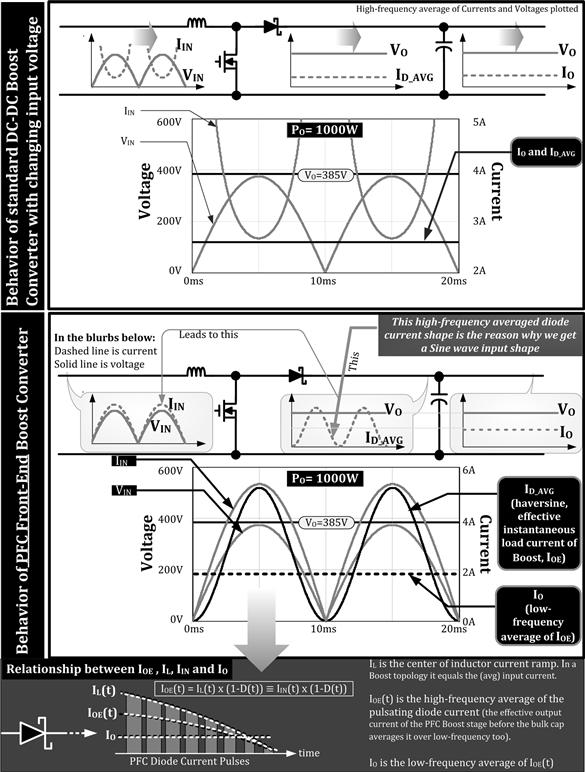
Figure 14.5: How a PFC Boost stage behaves as compared to a standard DC–DC Boost converter.
Let us see what steps we can take to make the standard Boost converter appear as a resistor to the source. The culprit is clearly our enforced requirement of a constant instantaneous output power, which in turn translated into a constant input power requirement. Naturally, the current increased when the voltage was low, rather than decrease as in any resistor. In principle, we want to create some type of control loop that does the following (however it actually implements it): we want to lower the effective (instantaneous) load current requirement as seen by the Boost stage to zero when the input voltage is zero, so that IO/(1 – D), which is the input current level of a Boost (center of ramp) remains finite. If we can accomplish that, we ask: can we appropriately “tailor” the instantaneous load current requirement, so that besides just limiting the input current to finite values, we actually get a pure sine-wave current at the input? In principle, there is no reason why we can’t do that. The only question is: what should the load current shape be to accomplish that? We can peek at the lower schematic of Figure 14.5 as we go along for the next part of the discussion.
Setting a time-varying instantaneous output current IOE(t), we get
![]()
IOE(t) is the effective (or instantaneous) load current as seen by the switching Boost converter. In other words, if we average out the high-frequency content of the current pulses passing through the PFC diode, we will no longer be left with a steady DC level “IO”, as in any conventional Boost converter, but a slowly varying current waveshape – one with a significant low-frequency component. This current waveform is called “IOE(t)”. Of course the load, connected to the right of the Boost output cap, demands a constant current. So, the bulk cap is now responsible for smoothening out, not only the high-frequency component of the diode current pulses, but also its slowly varying low-frequency component, and then passing that smoothened current as IO to the load.
Basically, any Boost PFC IC, irrespective of its actual implementation, ends up programming this correctly shaped load current profile, which then indirectly leads to the observed sine-wave input current. This was also indicated in the lower schematic of Figure 14.5. But keep in mind, that despite the seemingly big difference between the two schematics in Figure 14.5, at any given moment, the PFC Boost converter is (a) certainly in quasi steady state, and therefore, (b) if we set the appropriate load current at a given instant, all our known CCM DC–DC Boost converter equations are still valid at that instant. Because, the underlying topology is unchanged: it is still a Boost topology, just one with a slowly varying load profile.
Here is the math that tells us the required load current waveshape to achieve PFC. We first set the requirement and then work backwards.
![]()
K is an arbitrary constant so far. The input voltage is a rectified sine wave of peak value VIPK, with the same phase. So
![]()
The ratio of the input current and input voltage is thus independent of time and is called the “emulated resistance” RE.
![]()
This is what we wanted to achieve all along: the PFC stage (with a load connected to it as usual), appears as an emulated resistance RE to the AC source. We can also intuitively understand that if the load connected to the PFC stage starts demanding more power, RE must decrease to allow more current to flow in from the AC Source into the PFC stage. So we expect RE to be inversely proportional to PO, the output power of the PFC stage.
Note that we can typically assume that the PFC stage has a very high efficiency (greater than 90%, often approximated to 100% for simplicity). So the input power of the PFC stage is almost equal to its output power. That output power then becomes the input power of the PWM stage that follows. The PWM stage has a typical efficiency of about 70–80% and its output power is thus correspondingly lower. However, here we are talking strictly in terms of the input and output power relationships of the Boost PFC stage alone. We thus write
Since VAC=VIPK/√2, we get
![]()
So, the proportionality factor K is
![]()
Now considering each instant of the PFC stage as a Boost converter with a certain varying input, we know that the input current is
![]()
We already know that
![]()
Therefore we get
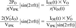
Solving, the desired equation of the instantaneous load current (required to create a sine-wave current input) is
![]()
In other words, we need IOE(t) to be of the form sin2(xt) if we want to get a sine-wave current at the input. That is the golden requirement for any PFC Boost stage, using any controller IC.
Note that the load current IO passes through the geometrical center of the IOE(t) curve (see Figure 14.5 carefully). That stands to reason, since the average of IOE(t) over a full AC half-cycle must equal the load current of the PFC Boost stage – a capacitor just smoothens, it cannot add any net current component.
We look more carefully at the plots inside Figure 14.5 (generated from a Mathcad file), and realize that IOE(t) is a sin2(xt) function, and similar in shape to a sine (or cosine) function translated upwards so as to bring its lowest point coincident with the horizontal axis. This is called a “haversine”. By definition
![]()
So we can say “if the load current of a Boost stage with an AC voltage input, is programmed to be a haversine, we will get a sine-wave input current”. That is in a nutshell, what a CCM Boost PFC stage does, any controller IC specifics notwithstanding.
Having intuitively understood how a Boost PFC stage performs, we can look at the detailed calculations in Figure 14.6, Figure 14.7 and Figure 14.8 for all the necessary RMS/Average current equations required, including a numerical example for implementing holdup time in PFC front end stages.
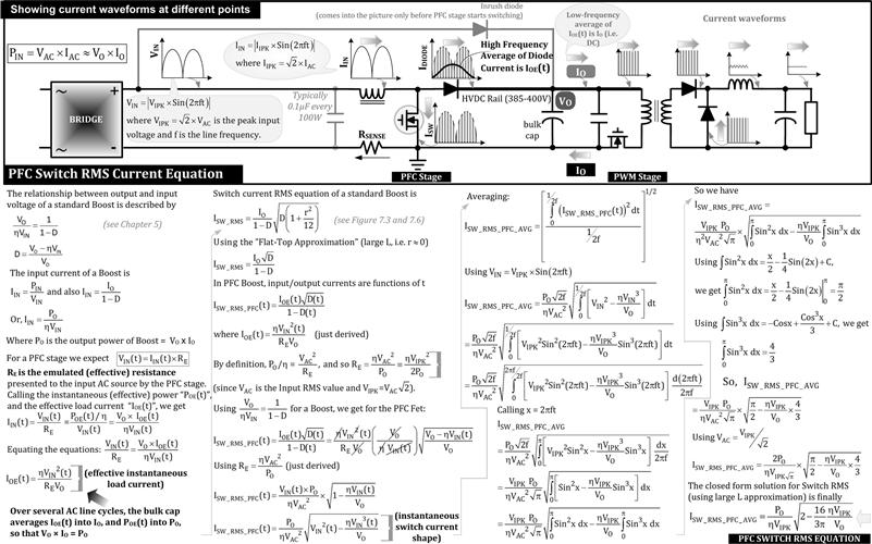
Figure 14.6: PFC switch RMS current equation.
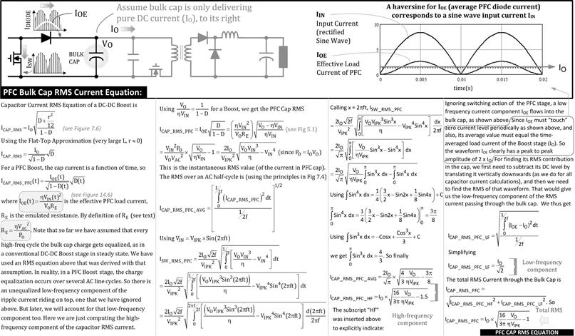
Figure 14.7: PFC input current and capacitor RMS equations.

Figure 14.8: PFC diode, filter, choke and capacitor holdup equations.
Finally, in Figure 14.9 we have presented the key variations graphically plotted with respect to line voltage. On the y-axis we have the currents per Amp of load current (flowing out of the bulk capacitor). For example, at a typical setting of 385 V for the high-voltage DC rail (‘HVDC’), this corresponds to 385 V/1 A=385 W power going into the PWM stage of. On the x-axis we have the ratio of conversion VIPK/VO. A numerical example is also provided alongside.
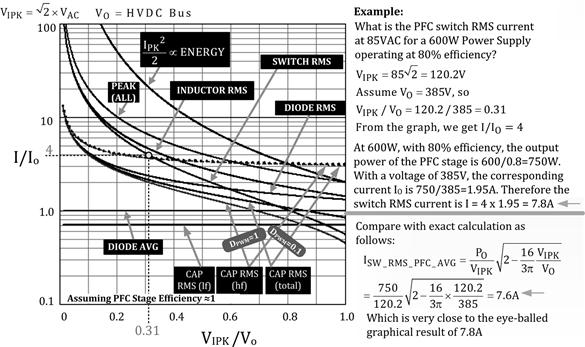
Figure 14.9: Quick lookup curves for estimating current stresses in the PFC stage.
Anti-Synchronization Technique for PFC and PWM Stages
Some power factor control ICs offer “synchronization capability” but that phrase usually means that the PFC stage is in-phase with the PWM stage. In other words, whenever the PFC switch turns ON, so does the PWM switch. In contrast, out-of-phase (anti) synchronization offers a dramatic reduction in the ripple rating (and cost) of the bulk cap.
Note: We had talked about this for the low-power AC–DC front end too. In the case of a PFC front end, because of the high bus voltage (~385 V), a typical 20–40 ms holdup time spec is met rather easily and automatically even for smaller capacitors. Therefore, the dominant factor, one that ultimately determines the final selection of the bulk cap in PFC designs, is not the holdup time, but the capacitor’s ripple rating (the RMS current passing through it). So this anti-synchronization scheme does translate into significant cost savings.
This anti-synchronization scheme was introduced as a combo IC a few years ago, and billed as the industry’s first “leading edge/trailing edge modulation scheme” PFC/PWM controller IC. What this IC essentially tried to accomplish was based on the following intuitive thought process: we know that the PWM draws current out from the bulk capacitor, whereas the PFC dumps current into it. What if we could make these opposing currents cancel out inside the cap (i.e. no resultant current)? In other words, what we want to do is to turn ON the PWM switch at the very same moment the PFC switch turns OFF. This is an out-of-phase (or anti-synchronization). But the (varying) duty cycle of the PFC stage at any given instant is not necessarily going to be the same as the (constant) duty cycle of the PWM stage. So the cancelation cannot be perfect. However, viewed in its entirety over one AC half-cycle, we can certainly assert that a good part of the freewheeling (diode) current on an average, will head straight into the PWM stage without getting recycled through the bulk capacitor, thus saving the latter from a good deal of RMS heating. Because of the duty cycle mismatch, it is hard to provide any easy closed-form equation for calculating the net reduction in the RMS current through the capacitor. So, not surprisingly, there was in fact no such detailed application information provided for the combo IC mentioned above, and could also be the reason why it never caught on. However there are several commercial products, especially in Europe, that have since, successfully used this technique for years, possibly based on practical in-house experience and know-how.
Note: The combo IC also had a crippling design flaw actually. It had a single shutdown pin, that when activated turned OFF both the PFC and PWM stages together. In practice, we want more flexibility. For example, we may want to turn-off the switching FET of the PFC stage quickly to protect it against a momentary line fault condition, but keep the PWM section running in the interim for holdup purposes. Or we may want to turn OFF the switching FET of the PWM stage (only), to turn its output OFF when demanded. In that case we would prefer to keep the PFC stage switching along, albeit at almost zero load, so that when the output of the power supply is asked to resume again, there is no long waiting time for the PFC stage to come back up from scratch.
The combo-IC we talked about above, had an unnecessary complication too. It had a clock of fixed frequency as usual. But whereas the PWM switch would turn ON at the clock edge (normal technique), the PFC would switch OFF at the clock edge. We remember that in most power converters, regulation is achieved by varying the moment at which the switch turns OFF, whereas the turn-on is determined by a clock. That is traditional ‘trailing-edge’ modulation. So, in this combo IC, the PWM worked in the conventional way, but the PFC used (opposite) ‘leading-edge’ modulation. The moment of turn-off was pre-ordained (due to the anti-synchronization demand), so the turn-on edge had to be varied to produce regulation. In effect, we now have to regulate the PFC pulse width knowing beforehand that the PFC switch must turn OFF at a certain moment and then reverse-calculate the exact moment we need to turn the PFC switch ON. No doubt this is all done silently by the control loop, but it does lead to rather complicated stability characteristics. So, to avoid this, in actual lab experiments conducted by the author in Germany, it was obvious that an easier way using standard parts was also possible. A UC3854 PFC-IC was used along with a common UC3844 PWM IC. The two ICs were synchronized (with a small resistor in series with the timing capacitor of the UC3854), such that the turn-off edge of the 3844 output reset the clock of the UC3854. So now the 3854 turns ON at the exact moment the 3844 turns OFF. Both are now performing trailing-edge modulation. The only change is that, in effect, the clock (and switch turn-on moment) of the UC3854 has been somewhat handed over to the UC3844 to control. In principle we could also reverse the order: use the UC3854 as the ‘master’ to have the 3844 turn ON the moment the 3854 turned OFF. This also works (but remember that the designated slave must always have a slightly lower set frequency than the master, to allow the master to dominate it slightly and safely). Both schemes were tried out on the bench and verified using Mathcad. Intuitively, in the latter case, a slight inherent line frequency modulation was expected at the output of the PWM stage. However, in practice, no such modulation was observed on the bench prototype. So both techniques worked – both being trailing-edge schemes, and both with PFC-PWM anti-synchronization at work.
In Figure 14.10 we have plotted out the ripple currents for 90VAC and 270VAC respectively, vs. the PWM stage duty cycle. We see that using synchronization, we get the highest percentage improvement at low line (only the total RMS is shown). The corresponding numbers are provided in the embedded table for quick lookup.
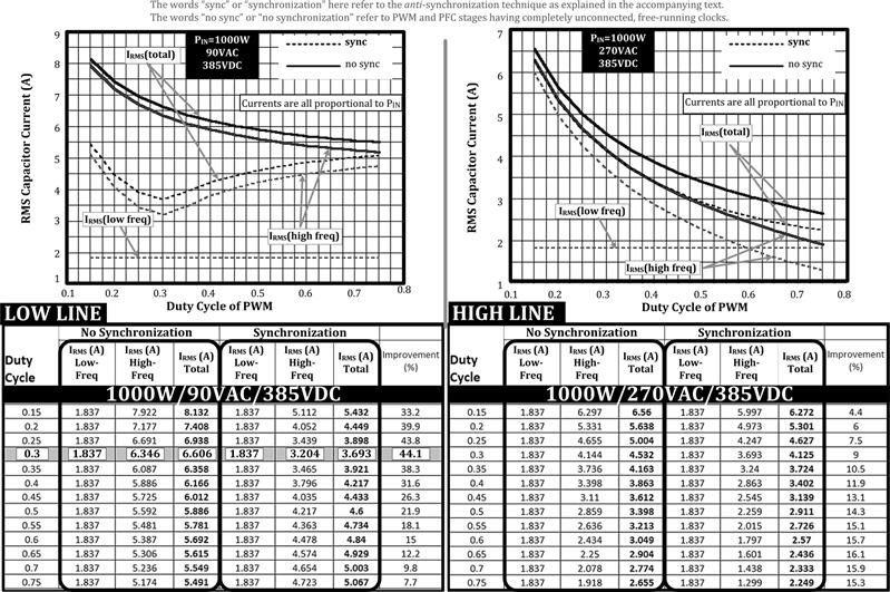
Figure 14.10: Quick lookup curves and tables for PFC-PWM anti-synchronization.
We must not forget that a capacitor is chosen not on the basis of a perceived ripple current “improvement”, but on the actual ripple current through it. We may see a big “improvement” as compared to what it would have been at that particular input voltage without synchronization, but the question is: what is its absolute value and its worst-case? We should evaluate both extremes of input voltage, and pick the higher of all the RMS currents thus reported. That would be the worst case number to check the capacitor rating against, i.e. the criterion for its selection.
The conclusions from the embedded table in Figure 14.10 are
(a) The maximum improvement (and the lowest absolute value) for the RMS current is at around DPWM=0.325. With a conventional single-ended Forward converter with a duty cycle set to about 0.3–0.35, the improvement due to synchronization is less than around 40%.
(b) In fact over the duty cycle range of 0.23–0.4, we can expect more than 32% improvement.
Capacitor RMS Current Calculations With and Without Anti-Synchronization
For the purpose of estimating the life of the Aluminum capacitor we need to know the breakup of the RMS components with respect to frequency as explained in Chapter 6. Note that very often, for the PFC stage, we implicitly assume PIN ≈ PO because of the typically (>90%) efficiency. Here is a sample calculation for capacitor selection.
Example
We have a worldwide (universal) input 70 W flyback running off the PFC stage. Its efficiency is 70%. What are the components of the capacitor RMS current at a set duty cycle of 50% at 90VAC?
In terms of the power rating of the PFC stage, we have 70 W/0.7=100 W. Let us first calculate the results assuming an input power of 1000 W since that is our reference baseline in Figure 14.10. With an HVDC of 385 V, the load current is (for 1000 W)
![]()
The total unsynchronized RMS current in the Bulk Cap at 90VAC is
![]()
Note that we have added a term above, with the duty cycle of the PWM stage, since that also contributes to the heating in the PFC cap.
Above, we have the result for 1000 W. So for a 100 W PFC stage this current would be 0.58 A, that being the number to select the bulk capacitor had there been no synchronization.
If we use anti-synchronization, the stated improvement from the table in Figure 14.10 is 21.855%. So then the RMS current requirement for a 1000 W converter would be
![]()
For a 100 W case we would pick an RMS rating of 0.46 A, much lower than 0.59 A (unsynchronized) above.
We also know that the low-frequency component of a 1000 W PFC stage is
![]()
Therefore its high-frequency component is
![]()
All the above numbers assume a 1000 W converter. So for our 100 W PFC stage, the high-frequency and low-frequency components of the RMS current are therefore 0.42 A and 0.18 A respectively. Knowing the frequency multiplier for the chosen capacitor family, we can now normalize these values to be an equivalent low-frequency current as explained in Chapter 6, and thus select our capacitor.
Note: We should remember that after the above wide input comparison based calculation, we don’t know (and don’t need to know) whether the (worst case) synchronized RMS calculated above occurs at high line or at low line. For selection of the capacitor, the above information is sufficient.
Interleaved Boost PFC Stages
In Chapter 13, we discussed interleaving as a method of reducing input and output capacitor RMS currents. So, besides the anti-synchronization scheme above, another option to save cost on the output cap of a PFC Boost stage is by interleaving. Please read Chapter 13 for more details on interleaving, keeping in mind that in Chapter 9 we showed that the Boost converter is a Buck converter with the input and output swapped. So it is easy to understand and quantify the benefits interleaving brings to multiple PFC stages sharing an output capacitor.
Practical Issues in Designing PFC Stages
(a) A critical component of a commercial PFC implementation is an inrush diode placed directly from the positive terminal of the bridge rectifier to the positive terminal of the PFC bulk cap (see Figure 14.6). This allows the bulk capacitor to charge up quickly when AC power is initially applied to the power supply, and helps keep the huge inrush current away from the PFC section’s choke and output diode. But this inrush diode is also a key reliability issue for the entire power supply. It is the component most likely to fail under repeated application of AC input. It need not be a fast diode as it goes out of the picture as soon as the PFC FET starts switching. It does not get hot either, and can be an axial or SMD component. But its non-repetitive surge rating must be high. For example, a slow diode like the 1N5408 (but from a quality vendor) is usually suitable since it has a much higher surge rating than the ultrafast diodes some designers seem to prefer in this position for no obvious reason.
(b) The biggest hit in efficiency in a PFC Boost stage usually comes from a severe shoot-through current spike originating from the bulk capacitor, that passes through the still-recovering PFC output diode whenever the PFC FET turns ON. This causes very high crossover losses in the PFC FET (not much observable impact in the diode itself). Therefore the PFC diode must be an extremely fast diode. Even a diode with more than 20–30 ns recovery time is unacceptable in this position except in very low-power and non-critical applications. That is one reason why for low-power applications engineers often prefer to use Boost PFC ICs that operate in critical conduction mode as discussed later.
(c) In low- to medium-power PFC stages, the lossless (inductor-based) “turn-on snubber”, which is considered virtually indispensable in high-power stages, may seem like a luxury. In that case some engineers like to reduce the reverse recovery current spike by replacing the single 600 V PFC diode with two 300 V diodes in series. Here they are relying on the fact that low-voltage diodes recover much faster than high-voltage diodes and so, despite their higher combined forward drop and consequent increased conduction losses, we actually improve efficiency by reducing the V×I crossover losses in the FET. But note, we cannot allow the full voltage to appear across either of the diodes at any moment, however brief. So they must be well-matched, especially in terms of their dynamic characteristics. That is not easy to do on a PCB, especially in mass production. Some engineers try to achieve matching by placing ballasting resistors across each diode (much as we do for capacitors placed in series for higher-voltage applications). But under dynamic conditions (as during switch transitions), this does not really help. A better option is to use two series diodes in one package, on the assumption that since they pass through exactly the same fabrication steps, they will automatically be well-matched. Some manufacturers even combine two series diodes on the very same chip for the best-possible dynamic matching. For example ST Microelectronics offers “Tandem diodes”. This may look like any other two-terminal diode, but in reality consists of two ultrafast recovery diodes in series, exhibiting higher forward drop, but excellent reverse recovery (~12 ns). Such diodes are often called “hyperfast”. An increasingly popular option nowadays is the 600 V silicon carbide (SiC) diode, as from Cree and Infineon. There is no need for any turn-on snubber either, just a SiC diode. This is becoming a popular option at medium- to high-power levels.
PFC Choke Design Guidelines
In Figure 14.11 we have presented the complete procedure for designing an air-gapped PFC ferrite choke. All the required equations are embedded in it. The key differences from previous procedures that we used (in particular in Chapter 5) are as follows:
(A) Since the input voltage is constantly changing, we have to identify not only which AC voltage, but which instantaneous voltage point within its sine waveform, creates the maximum peak currents. Only then can we really ensure the PFC core does not saturate over its entire range of operation. From Figure 14.9, we see that the max peak input current occurs at low-line its very peak. We thus decide to size the core at VAC_MIN_PEAK. That is 85×√2=120.2VDC (or at 127VDC corresponding to a minimum of 90VAC) (certainly not at VSAG as for low-power front end designs).
(B) The air gap factor “z” we had defined in Chapter 5 is
![]()
For large air gaps (large z), we can approximate z to
![]()
For E-type ferrite transformers, we had previously recommended z of 10 as a good target. That amounts to an le/lg of 10/2000=0.5%. However in a choke, since there is no Secondary winding, we can virtually double the number of (Primary) turns that can be accommodated in the available window. Since z depends of turns squared (for a given inductance), what we are saying is that a z of 40 or equivalently, an “le/lg of 2%”, is recommended for a ferrite PFC choke. So that becomes our design target here.
(C) The current ripple ratio r. This is traditionally set to 0.4, but in a PFC stage it is hard to decide its optimum value, since the input voltage is varying as a sine wave. In the next section we will see that the ΔIL of the choke is actually much higher at 180VAC than at low AC line voltages (or at high). This can lead to higher input filtering costs than expected. So, to keep costs down, when we design the choke at low-line, we leave margin for this increase in current swing at higher voltages, by fixing r to a more optimum value of 0.2, instead of the traditional 0.4 (i.e. set ±10% current ripple, instead of ±20%). That is our design target in the examples in Figure 14.11.

Figure 14.11: PFC choke design equations and an example.
Core Losses in PFC Choke
We can refer to Chapter 2 to see how to calculate the core loss for a steady DC input. The important thing to keep in mind is that core losses do not depend of the DC pedestal of current (IL), only on the swing ΔIL. And that swing is the peak to peak current swing, which in turn translates into a proportional flux density swing. But the problem with PFC is that the input is varying even at a given line voltage VAC, and further, also as that voltage varies with the applied VAC. Under each condition, the current swing is so different that it seems impossible to estimate the core losses, or even their average value, for the purpose of better estimating temperature rise of the choke.
In Figure 14.12 we have shown a mathematical simulation of the inductor current. Note that the high frequency is scaled down for visual clarity, but since the inductance used in the simulation is proportionately scaled upwards, the peaks, troughs and the peak to peak values of the currents shown are in fact the actual values we will see under the application conditions indicated in the figure.
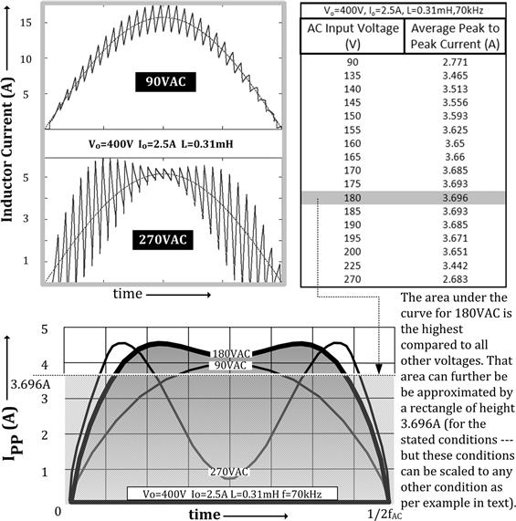
Figure 14.12: Mathematical simulation of inductor current in Boost choke.
Using the same Mathcad file used to plot Figure 14.12, it can be observed that at 180VAC, the peak to peak current has a shape closest to a rectangular shape (and the highest average, see the embedded table in the figure). The values in the table are for an HVDC rail of 400 V and a current of 2.5 A. So this is a 1000 W PFC stage. The way things scale is shown in the following example.
Example
We have a worldwide input 500 W PFC stage (assume 90% efficiency). It uses a choke inductance of 0.5 mH, and its switching frequency is 100 kHz. What is the average ΔI we should use in core loss estimation?
From the embedded table in Figure 14.12, we have the worst case average current swing over all AC (line) and sine-wave variations (under the stated conditions) as 3.7 A. We can scale this to our current conditions as follows
![]()
The steady DC current (or power) does not come into the picture as expected (only indirectly via the choice of inductance). The associate average ΔB can be calculated using Faraday’s law with a knowledge of the core characteristics and the number of turns. The average core loss so calculated will then accurately reflect the actual averaged value, over the entire universal input range. See Chapter 2 for the detailed core loss calculation procedure in DC–DC converters.
Borderline Active PFC using Boost
So far we have been discussing active PFC running in CCM (continuous conduction mode). For low to medium power, a popular option is “borderline PFC” (borderline conduction mode is called BCM, see Chapter 1). BCM-PFC is almost the same as CCM-PFC, except that the PFC FET waits till the inductor current ramps down to zero before turning ON again. In effect we are forcing the inductor to operate in critical conduction mode. The main advantage of doing that is the PFC diode current is zero whenever the PFC FET turns ON. So, borderline Boost PFC stages have no “PFC diode reverse recovery shoot-through” problem. They do not need turn-on snubbers. But they do work with variable frequency and so their EMI filtering can pose a problem.
What are their stress equations? To answer that, keep in mind that BCM (also called critical conduction mode) is a special case of CCM with r=2. Admittedly BCM is on the extreme end, but still a member of CCM. Further, we recognize that RMS/Avg equations do not depend on the switching frequency, only on duty cycle D. In other words, all the stress equations we have calculated so far, should still apply – in principle. But they really don’t! Because on closer examination we see that in all the previous CCM-PFC derivations, we used the “flat-top approximation”. This assumes a very small r (large L). Which is why none of the stress equations we derived (or any available in literature) include “r” (or equivalently L). In other words, our PFC stress equations are an approximation to start with.
In BCM, r has a value of 2. But we have already assumed r to be almost zero! That is the reason why, though our CCM equations are still valid in principle for BCM, they will not give accurate answers. This is pointed out because many engineers (and textbooks) mistakenly apply the CCM equations to BCM. Note also that the current swing is much more in BCM, and so are the core losses, along with the entire design of the PFC choke. The peak currents are much higher. Borderline PFC design is just not trivial. We will therefore avoid it here, justified on the grounds that in any case, PFC is really required for fairly high power applications. Further, with the growing popularity of SiC diodes, our opinion is we should now focus exclusively on CCM-PFC, which is far more predictable in terms of its EMI spectrum and required input filtering. Certainly no passive PFC or flyback-based PFC, or valley-fill PFC as discussed previously.