
Chapter 1
The Principles of Switching Power Conversion
This is the entry point into the field of switching power conversion. It starts from the very basics: the charging and discharging of a capacitor and attempts to develop a parallel intuition for the way an inductor behaves when it is carrying current. Replete with real-world analogies, it shows the importance of providing a freewheeling path for the inductor current. That angle of approach eventually leads to the evolution of switching topologies. It also becomes very clear why there are only three fundamental topologies. The voltseconds law in steady state is explained and how that leads to the underlying DC transfer function. Basic converter operation including continuous and discontinuous conduction modes is also discussed.
Introduction
Imagine we are at some busy “metro” terminus one evening at peak hour. Almost instantly, thousands of commuters swarm the station trying to make their way home. Of course, there is no train big enough to carry all of them simultaneously. So, what do we do? Simple! We split this sea of humanity into several trainloads — and move them out in rapid succession. Many of these outbound passengers will later transfer to alternative forms of transport. So, for example, trainloads may turn into bus-loads or taxi-loads, and so on. But eventually, all these “packets” will merge once again, and a throng will be seen, exiting at the destination.
Switching power conversion is remarkably similar to a mass transit system. The difference is that instead of people, it is energy that gets transferred from one level to another. So we draw energy continuously from an “input source,” chop this incoming stream into packets by means of a “switch” (a transistor), and then transfer it with the help of components (inductors and capacitors) that are able to accommodate these energy packets and exchange them among themselves as required. Finally, we make all these packets merge again and thereby get a smooth and steady flow of energy into the output.
So, in either of the cases above (energy or people), from the viewpoint of an observer, a stream will be seen entering and a similar one exiting. But at an intermediate stage, the transference is accomplished by breaking up this stream into more manageable packets.
Looking more closely at the train station analogy, we also realize that to be able to transfer a given number of passengers in a given time (note that in electrical engineering, energy transferred in unit time is “power”) — either we need bigger trains with departure times spaced relatively far apart OR several smaller trains leaving in rapid succession. Therefore, it should come as no surprise that in switching power conversion, we always try to switch at high frequencies. The primary purpose for that is to reduce the size of the energy packets and thereby also the size of the components required to store and transport them.
Power supplies that use this principle are called “switching power supplies” or “switching power converters.”
“DC–DC converters” are the basic building blocks of modern high-frequency switching power supplies. As their name suggests, they “convert” an available DC (direct current) input voltage rail “VIN” to another more desirable or usable DC output voltage level “VO.” “AC–DC converters” (see Figure 1.1), also called “off-line power supplies,” typically run off the mains input (or “line input”). But they first rectify the incoming sinusoidal AC (alternating current) voltage “VAC” to a DC voltage level (often called the “HVDC rail” or “high voltage DC rail”) — which then gets applied at the input of what is essentially just another DC–DC converter stage (or derivative thereof). We thus see that power conversion is, in essence, almost always a DC–DC voltage conversion process.
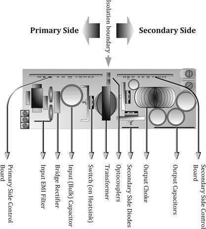
Figure 1.1: Typical off-line power supply.
But it is also equally important to create a steady DC output voltage level, from what can often be a widely varying and different DC input voltage level. Therefore, a “control circuit” is used in all power converters to constantly monitor and compare the output voltage against an internal “reference voltage.” Corrective action is taken if the output drifts from its set value. This process is called “output regulation” or simply “regulation.” Hence, the generic term “voltage regulator” for supplies which can achieve this function, switching, or otherwise.
In a practical implementation, “application conditions” are considered to be the applied input voltage VIN (also called the “line voltage”), the current being drawn at the output, that is, IO (the “load current”), and the set output voltage VO. Temperature is also an application condition, but we will ignore it for now, since its effect on the system is usually not so dramatic. Therefore, for a given output voltage, there are two specific application conditions whose variations can cause the output voltage to be immediately impacted (were it not for the control circuit). Maintaining the output voltage steady when VIN varies over its stated operating range VINMIN to VINMAX (minimum input to maximum input) is called “line regulation,” whereas maintaining regulation when IO varies over its operating range IOMIN to IOMAX (minimum-to-maximum load) is referred to as “load regulation.” Of course, nothing is ever “perfect,” so nor is the regulation. Therefore, despite the correction, there is a small but measurable change in the output voltage, which we call “ΔVO” here. Note that mathematically, line regulation is expressed as “ΔVO/VO×100% (implicitly implying it is over VINMIN to VINMAX).” Load regulation is similarly “ΔVO/VO×100%” (from IOMIN to IOMAX).
However, the rate at which the output can be corrected by the power supply (under sudden changes in line and load) is also important — since no physical process is “instantaneous.” So, the property of any converter to provide quick regulation (correction) under external disturbances is referred to as its “loop response” or “AC response.” Clearly, the loop response is in general, a combination of “step-load response” and “line transient response.”
As we move on, we will first introduce the reader to some of the most basic terminology of power conversion and its key concerns. Later, we will progress toward understanding the behavior of the most vital component of power conversion — the inductor. It is this component that even some relatively experienced power designers still have trouble with! Clearly, real progress in any area cannot occur without a clear understanding of the components and the basic concepts involved. Therefore, only after understanding the inductor well enough, can we go on to demonstrate the fact that switching converters are not all that mysterious either — in fact they evolve quite naturally out of a keen understanding of the inductor.
Overview and Basic Terminology
Efficiency
Any regulator carries out the process of power conversion with an “efficiency,” defined as
![]()
where PO is the “output power,” equal to
![]()
and PIN is the “input power,” equal to
![]()
Here, IIN is the average or DC current being drawn from the source.
Ideally we want η=1, and that would represent a “perfect” conversion efficiency of 100%. But in a real converter, that is, with η<1, the difference “PIN−PO” is simply the wasted power “Ploss” or “dissipation” (occurring within the converter itself). By simple manipulation, we get
![]()
![]()
![]()
This is the loss expressed in terms of the output power. In terms of the input power, we would similarly get
![]()
The loss manifests itself as heat in the converter, which in turn causes a certain measurable “temperature rise” ΔΤ over the surrounding “room temperature” (or “ambient temperature”). Note that high temperatures affect the reliability of all systems — the rule of thumb being that every 10°C rise causes the failure rate to double. Therefore, part of our skill as designers is to reduce this temperature rise and also achieve higher efficiencies.
Coming to the input current (drawn by the converter), for the hypothetical case of 100% efficiency, we get
![]()
So, in a real converter, the input current increases from its “ideal” value by the factor 1/η.
![]()
Therefore, if we can achieve high efficiency, the current drawn from the input (keeping application conditions unchanged) will decrease — but only up to a point. The input current clearly cannot fall below the “brickwall,” that is, “IIN_ideal,” because this current is equal to PO/VIN — that is, related only to the “useful power” PO, delivered by the power supply, which we are assuming has not changed.
Further, since
![]()
by simple algebra, the dissipation in the power supply (energy lost per second as heat) can also be written as
![]()
This form of the dissipation equation indicates a little more explicitly how additional energy (more input current for a given input voltage) is pushed into the input terminals of the power supply by the applied DC source — to compensate for the wasted energy inside the power supply — even as the converter continues to provide the useful energy PO being constantly demanded by the load.
A modern switching power supply’s efficiency can typically range from 65% to 95% — that figure being considered attractive enough to have taken switchers to the level of interest they arouse today and their consequent wide application. Traditional regulators (like the “linear regulator”) provide much poorer efficiencies — and that is the main reason why they are slowly but surely getting replaced by switching regulators.
Linear Regulators
“Linear regulators,” equivalently called “series–pass regulators,” or simply “series regulators,” also produce a regulated DC output rail from an input rail. But they do this by placing a transistor in series between the input and the output. Further, this “series–pass transistor” (or “pass transistor”) is operated in the linear region of its voltage–current characteristics — thus acting like a variable resistance of sorts. As shown in the uppermost schematic of Figure 1.2, this transistor is made to literally “drop” (abandon) the unwanted or “excess” voltage across itself.
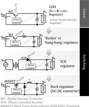
Figure 1.2: Basic types of linear and switching regulators.
The excess voltage is clearly just the difference “VIN−VO” — and this term is commonly called the “headroom” of the linear regulator. We can see that the headroom needs to be a positive number always, thus implying VO<VIN. Therefore, linear regulators are, in principle, always “step-down” in nature — that being their most obvious limitation.
In some applications (e.g., battery-powered portable electronic equipment), we may want the output rail to remain well regulated even if the input voltage dips very low — say down to within 0.6 V or less of the set output level VO. In such cases, the minimum possible headroom (or “dropout”) achievable by the linear regulator stage may become an issue.
No switch is perfect, and even if held fully conducting, it does have some voltage drop across it. So the dropout is simply the minimum achievable “forward-drop” across the switch. Regulators which can continue to work (i.e., regulate their output), with VIN barely exceeding VO, are called “low-dropout” regulators or “LDOs.” But note that there is really no precise voltage drop at which a linear regulator “officially” becomes an LDO. So the term is sometimes applied rather loosely to linear regulators in general. However, the rule of thumb is that a dropout of about 200 mV or lower qualifies as an LDO, whereas older devices (conventional linear regulators) have a typical dropout voltage of around 2 V. There is also an intermediate category called “quasi-LDOs” that have a dropout of about 1 V, that is, somewhere in between the two.
Besides being step-down in principle, linear regulators have another limitation — poor efficiency. Let us understand why that is so. The instantaneous power dissipated in any device is by definition the cross-product V×I, where V is the instantaneous voltage drop across it and I the instantaneous current through it. In the case of the series–pass transistor, under steady application conditions, both V and I are actually constant with respect to time — V in this case being the headroom VIN−VO and I the load current IO (since the transistor is always in series with the load). So we see that the V×I dissipation term for linear regulators can, under certain conditions, become a significant proportion of the useful output power PO. And that simply spells “poor efficiency”! Further, if we stare hard at the equations, we will realize there is also nothing we can do about it — how can we possibly argue against something as basic as V×I? For example, if the input is 12 V, and the output is 5 V, then at a load current of 100 mA, the dissipation in the regulator is necessarily ΔV×IO=(12–5) V×100 mA=700 mW. The useful (output) power is, however, VO×IO=5 V×100 mA=500 mW. Therefore, the efficiency is PO/PIN=500/(700+500)=41.6%. What can we do about that? Blame Georg Ohm?
On the positive side, linear regulators are very “quiet” — exhibiting none of the noise and electromagnetic interference (EMI) that have unfortunately become a “signature” or “trademark” of modern switching regulators. Switching regulators need filters — usually both at the input and at the output, to quell some of this noise, which can interfere with other gadgets in the vicinity, possibly causing them to malfunction. Note that sometimes the usual input/output capacitors of the converter may themselves serve the purpose, especially when we are dealing with “low-power” (and “low-voltage”) applications. But in general, we may require filter stages containing both inductors and capacitors. Sometimes these stages may need to be cascaded to provide even greater noise attenuation.
Achieving High Efficiency through Switching
Why are switchers so much more efficient than “linears”?
As their name indicates, in a switching regulator, the series transistor is not held in a perpetual partially conducting (and therefore dissipative) mode — but is instead switched repetitively. So there are only two states possible — either the switch is held “ON” (fully conducting) or it is “OFF” (fully nonconducting) — there is no “middle ground” (at least not in principle). When the transistor is ON, there is (ideally) zero voltage across it (V=0), and when it is OFF, we have zero current through it (I=0). So, it is clear that the cross-product “V×I” is also zero for either of the two states. And that simply implies zero “switch dissipation” at all times. Of course, this too represents an impractical or “ideal” case. Real switches do dissipate. One reason for that is they are never either fully ON nor fully OFF. Even when they are supposedly ON, they have a small voltage drop across them, and when they are supposedly “OFF,” a small current still flows through them. Further, no device switches “instantly” either — there is always a definable period in which the device is transiting between states. During this interval too, V×I is not zero and some additional dissipation occurs.
We may have noticed that in most introductory texts on switching power conversion, the switch is shown as a mechanical device — with contacts that simply open (“switch OFF”) or close (“switch ON”). So, a mechanical device comes very close to our definition of a “perfect switch” — and that is the reason why it is often the vehicle of choice to present the most basic principles of power conversion. But one obvious problem with actually using a mechanical switch in any practical converter is that such switches can wear out and fail over a relatively short period of time. So in practice, we always prefer to use a semiconductor device (e.g., a transistor) as the switching element. As expected, that greatly enhances the life and reliability of the converter. But the most important advantage is that since a semiconductor switch has none of the mechanical “inertia” associated with a mechanical device, it gives us the ability to switch repetitively between the ON and OFF states — and does so very fast. We have already realized from the metro terminus analogy on page 1 that that will lead to smaller components in general.
We should be clear that the phrase “switching fast,” or “high switching speed,” has slightly varying connotations, even within the area of switching power conversion. When it is applied to the overall circuit, it refers to the frequency at which we are repeatedly switching — ON OFF, ON OFF, and so on. This is the converter’s basic switching frequency “f” (in Hz). But when the same term is applied specifically to the switching element or device, it refers to the time spent transiting between its two states (i.e., from ON to OFF and OFF to ON) and is typically expressed in “ns” (nanoseconds). This transition interval is then rather implicitly and intuitively being compared to the total “time period” T (where T=1/f) and therefore to the switching frequency — though we should be clear there is no direct relationship between the transition time and the switching frequency.
We will learn shortly that the ability to crossover (i.e., transit) quickly between switching states is in fact rather crucial. Yes, up to a point, the switching speed is almost completely determined by how “strong” and effective we can make our external “drive circuit.” But ultimately, the speed becomes limited purely by the device and its technology — an “inertia” of sorts at an electrical level.
Basic Types of Semiconductor Switches
Historically, most power supplies used the bipolar junction transistor (BJT) shown in Figure 1.2. It is admittedly a rather slow device by modern standards. But it is still relatively cheap! In fact its “NPN” version is even cheaper and therefore more popular than its “PNP” version. Modern switching supplies prefer to use a “MOSFET” (metal oxide semiconductor field effect transistor), often simply called a “FET” (see Figure 1.2 again). This modern high-speed switching device also comes in several “flavors” — the most commonly used ones being the N-channel and P-channel types (both usually being the “enhancement mode” variety). The N-channel MOSFET happens to be the favorite in terms of cost effectiveness and performance for most applications. However, sometimes, P-channel devices may be preferred for various reasons — mainly because they usually require simpler drive circuits.
Despite the steady course of history in favor of MOSFETs in general, there still remain some arguments for continuing to prefer BJTs in certain applications. Some points to consider and debate here are:
a. It is often said that it is easier to drive a MOSFET than a BJT. In a BJT, we do need a large drive current (injected into its “base” terminal) — to turn it ON. We also need to keep injecting base current to keep it in that state. On the other hand, a MOSFET is considered easier to drive. In theory, we just have to apply a certain voltage at its “Gate” terminal to turn it ON and also keep it that way. Therefore, a MOSFET is called a “voltage-controlled” device, whereas a BJT is considered a “current-controlled” device. However, in reality, a modern MOSFET needs a certain amount of Gate current during the time it is in transit (ON to OFF and OFF to ON). Further, to make it change state fast, we may in fact need to push in (or pull out) a lot of current (typically 1 to 2A).
b. The drive requirements of a BJT may actually turn out easier to implement in many cases. The reason for that is, to turn an NPN BJT ON for example, its Gate has to be taken only about 0.8 V above its Emitter (and can even be tied directly to its Collector on occasion), whereas in an N-channel MOSFET, its Gate has to be taken several volts higher than its Source. Therefore, in certain types of DC–DC converters, when using an N-channel MOSFET, it can be shown that we need a “drive rail” that is significantly higher than the (available) input rail VIN. And how else can we hope to have such a rail except by a circuit that can somehow manage to “push” or “pump” the input voltage to a higher level? When thus implemented, such a rail is called the “bootstrap” rail.
Note: The most obvious implementation of a “bootstrap circuit” may just consist of a small capacitor that gets charged by the input source (through a small signal diode) whenever the switch turns OFF. Thereafter, when the switch turns ON, we know that a certain voltage node in the power supply suddenly “flips” whenever the switch changes state. But since the “bootstrap capacitor”, one end of which is connected to this (switching) node, continues to hold on to its acquired voltage (and charge), its other end, which forms the bootstrap rail, gets pushed up to a level higher than the input rail as desired. This rail then helps drive the MOSFET properly under all conditions.
c. The main advantage of BJTs is that they are known to generate significantly less EMI and “noise and ripple” than MOSFETs. That ironically is a positive outcome of their slower switching speed!
d. BJTs are also often better suited for high-current applications — because their “forward drop” (on-state voltage drop) is relatively constant, even for very high switch currents. This leads to significantly lower “switch dissipation,” more so when the switching frequencies are not too high. On the contrary, in a MOSFET, the forward drop is almost proportional to the current passing through it — so its dissipation can become significant at high loads. Luckily, since it also switches faster (lower transition times), it usually more than makes up for that loss term, and so in fact becomes much better in terms of the overall loss — more so when compared at very high switching frequencies.
Note: In an effort to combine the “best of both worlds,” a “combo” device called the “IGBT” (insulated Gate bipolar transistor is also often used nowadays. It is driven like a MOSFET (voltage-controlled) but behaves like a BJT in other ways (the forward drop and switching speed). It too is therefore suited mainly for low-frequency and high-current applications but is considered easier to drive than a BJT.
Semiconductor Switches Are Not “Perfect”
We mentioned that all semiconductor switches suffer losses. Despite their advantages, they are certainly not the perfect or ideal switches we may have imagined them to be at first sight.
So, for example, unlike a mechanical switch, in the case of a semiconductor device, we may have to account for the small but measurable “leakage current” flowing through it when it is considered “fully OFF” (i.e., nonconducting). This gives us a dissipation term called the “leakage loss.” This term is usually not very significant and can be ignored. However, there is a small but significant voltage drop (“forward drop”) across the semiconductor when it is considered “fully ON” (i.e., conducting) — and that gives us a significant “conduction loss” term. In addition, there is also a brief moment as we transition between the two switching states, when the current and voltage in the switch need to slew up or down almost simultaneously to their new respective levels. So, during this “transition time” or “crossover time,” we have neither V=0 nor I=0 instantaneously, and therefore nor is V×I=0. This therefore leads to some additional dissipation and is called the “crossover loss” (or sometimes just “switching loss”). Eventually, we need to learn to minimize all such loss terms if we want to improve the efficiency of our power supply.
However, we must remember that power supply design is by its very nature full of design tradeoffs and subtle compromises. For example, if we look around for a transistor with a very low forward voltage drop, possibly with the intent of minimizing the conduction loss, we usually end up with a device that also happens to transition more slowly — thus leading to a higher crossover loss. There is also an overriding concern for cost that needs to be constantly looked into, particularly in the commercial power supply arena. So, we should not underestimate the importance of having an astute and seasoned engineer at the helm of affairs, one who can really grapple with the finer details of power supply design. As a corollary, neither can we probably ever hope to replace him or her (at least not entirely), by some smart automatic test system, nor by any “expert design software” that the upper management may have been dreaming of.
Achieving High Efficiency through the Use of Reactive Components
We have seen that one reason why switching regulators have such a high efficiency is because they use a switch (rather than a transistor that “thinks” it is a resistor, as in an LDO). Another root cause of the high efficiency of modern switching power supplies is their effective use of both capacitors and inductors. Capacitors and inductors are categorized as “reactive” components because they have the unique ability of being able to store energy. However, that is also why they cannot ever be made to dissipate energy either (at least not within themselves) — they just store all the energy “thrown at them”! On the other hand, we know that “resistive” components dissipate energy but, unfortunately, can’t store any!
A capacitor’s stored energy is called electrostatic, equal to ![]() , where C is the “capacitance” (in Farads) and V the voltage across the capacitor. Whereas an inductor’s stored energy is called magnetic, equal to
, where C is the “capacitance” (in Farads) and V the voltage across the capacitor. Whereas an inductor’s stored energy is called magnetic, equal to ![]() with L being the “inductance” (in Henrys) and I the current passing through it (at any given moment).
with L being the “inductance” (in Henrys) and I the current passing through it (at any given moment).
But we may well ask — despite the obvious efficiency concerns, do we really need reactive components in principle! For example, we may have realized we don’t really need an input or output capacitor for implementing a linear regulator — because the series–pass element (the BJT) is all that is required to block any excess voltage. For switching regulators, however, the reasoning is rather different. This leads us to the general “logic of switching power conversion” summarized below.
• A transistor is needed to establish control on the output voltage and thereby bring it into regulation. The reason we switch it is as follows — dissipation in this control element is related to the product of the voltage across the control device and the current through it, that is V×I. So, if we make either V or I zero (or very small), we will get zero (or very small) dissipation. By switching constantly between ON and OFF states, we can keep the switch dissipation down, but at the same time, by controlling the ratio of the ON and OFF intervals, we can regulate the output, based on average energy flow considerations.
• But whenever we switch the transistor, we effectively disconnect the input from the output (during either the ON or the OFF state). However, the output (load) always demands a continuous flow of energy. Therefore, we need to introduce energy-storage elements somewhere inside the converter. In particular, we use output capacitors to “hold” the voltage steady across the load during the above-mentioned input-to-output “disconnect” interval.
• But as soon as we put in a capacitor, we now also need to limit the inrush current into it — all capacitors connected directly across a DC source will exhibit an uncontrolled inrush — and that can’t be good either for noise, for EMI, or for efficiency. Of course, we could simply opt for a resistor to subdue this inrush, and that in fact was the approach behind the early “bucket regulators” (Figure 1.2).
• But unfortunately a resistor always dissipates — so what we may have saved in terms of transistor dissipation may ultimately end up in the resistor! To maximize the overall efficiency, we therefore need to use only reactive elements in the conversion process. Reactive elements can store energy but do not dissipate any (in principle). Therefore, an inductor becomes our final choice (along with the capacitor), based on its ability to non-dissipatively limit the (rate of rise of) current, as is desired for the purpose of limiting the capacitor inrush current.
Some of the finer points in this summary will become clearer as we go on. We will also learn that once the inductor has stored some energy, we just can’t wish this stored energy away at the drop of a hat. We need to do something about it! And that in fact gives us an actual working converter down the road.
Early RC-Based Switching Regulators
As indicated above, a possible way out of the “input-to-output disconnect” problem is to use only an output capacitor. This can store some extra energy when the switch connects the load to the input, and then provide this energy to the load when the switch disconnects the load.
But we still need to limit the capacitor charging current (“inrush current”). And as indicated, we could use a resistor. That was in fact the basic principle behind some early linear-to-switcher “crossover products” like the bucket regulator shown in Figure 1.2.
The bucket regulator uses a transistor driven like a switch (as in modern switching regulators), a small series resistor to limit the current (not entirely unlike a linear regulator), and an output capacitor (the “bucket”) to store and then provide energy when the switch is OFF. Whenever the output voltage falls below a certain threshold, the switch turns ON, “tops up” the bucket, and then turns OFF. Another version of the bucket regulator uses a cheap low-frequency switch called an SCR (“semiconductor controlled rectifier”) that works off the Secondary windings of a step-down transformer connected to an AC mains supply, as also shown in Figure 1.2. Note that in this case, the resistance of the windings (usually) serves as the (only) effective limiting resistance.
Note also that in either of these RC-based bucket regulator implementations, the switch ultimately ends up being toggled repetitively at a certain rate — and in the process, a rather crudely regulated stepped-down output DC rail is created. By definition, that makes these regulators switching regulators too!
But we realize that the very use of a resistor in any power conversion process always bodes ill for efficiency. So, we may have just succeeded in shifting the dissipation away from the transistor — into the resistor! If we really want to maximize overall efficiency, we need to do away with any intervening resistance altogether.
So, we attempt to use an inductor instead of a resistor for the purpose — we don’t really have many other component choices left in our bag! In fact, if we manage to do that, we get our first modern LC-based switching regulator — the “Buck regulator” (i.e., step-down converter), as also presented in Figure 1.2.
LC-Based Switching Regulators
Though the detailed functioning of the modern Buck regulator of Figure 1.2 will be explained a little later, we note that besides the obvious replacement of R with an L, it looks very similar to the bucket regulator — except for a “mysterious” diode. The basic principles of power conversion will in fact become clear only when we realize the purpose of this diode. This component goes by several names — “catch diode,” “freewheeling diode,” “commutation diode,” and “output diode,” to name but a few! But its basic purpose is always the same — a purpose we will soon learn is intricately related to the behavior of the inductor itself.
Aside from the Buck regulator, there are two other ways to implement the basic goal of switching power conversion (using both inductors and capacitors). Each of these leads to a distinct “topology.” So besides the Buck (step-down), we also have the “Boost” (step-up), and the “Buck-Boost” (step-up or step-down). We will see that though all these are based on the same underlying principles, they are set up to look and behave quite differently. As a prospective power supply designer, we really do need to learn and master each of them almost on an individual basis. We must also keep in mind that in the process, our mental picture will usually need a drastic change as we go from one topology to another.
Note: There are some other capacitor-based possibilities — in particular “charge pumps” — also called “inductor-less switching regulators.” These are usually restricted to rather low powers and produce output rails that are rather crudely regulated multiples of the input rail. In this book, we are going to ignore these types altogether.
Then there are also some other types of LC-based possibilities — in particular the “resonant topologies.” Like conventional DC–DC converters, these also use both types of reactive components (L and C) along with a switch. However, their basic principle of operation is very different. Without getting into their actual details, we note that these topologies do not maintain a constant switching frequency, which is something we usually rather strongly desire. From a practical standpoint, any switching topology with a variable switching frequency can lead to an unpredictable and varying EMI spectrum and noise signature. To mitigate these effects, we may require rather complicated filters. For such reasons, resonant topologies have not really found widespread acceptance in commercial designs, and so we too will largely ignore them from this point on.
The Role of Parasitics
In using conventional LC-based switching regulators, we may have noticed that their constituent inductors and capacitors do get fairly hot in most applications. But if, as we said, these components are reactive, why at all are they getting hot? We need to know why, because any source of heat impacts the overall efficiency! And efficiency is what modern switching regulators are all about!
The heat arising from real-world reactive components can invariably be traced back to dissipation occurring within the small “parasitic” resistive elements, which always accompany any such (reactive) component.
For example, a real inductor has the basic property of inductance L, but it also has a certain non-zero DC resistance (“DCR”) term, mainly associated with the copper windings used. Similarly, any real capacitor has capacitance C, but it also has a small equivalent series resistance (“ESR”). Each of these terms produces “ohmic” losses — that can all add up and become fairly significant.
As indicated previously, a real-world semiconductor switch can also be considered as having a parasitic resistance “strapped” across it. This parallel resistor in effect “models” the leakage current path and thus the “leakage loss” term. Similarly, the forward drop across the device can also, in a sense, be thought of as a series parasitic resistance — leading to a conduction loss term.
But any real-world component also comes with various reactive parasitics. For example, an inductor can have a significant parasitic capacitance across its terminals — associated with electrostatic effects between the layers of its windings. A capacitor can also have an equivalent series inductance (“ESL”) — coming from the small inductances associated with its leads, foil, and terminations. Similarly, a MOSFET also has various parasitics — for example, the “unseen” capacitances present between each of its terminals (within the package). In fact, these MOSFET parasitics play a major part in determining the limits of its switching speed (transition times).
In terms of dissipation, we understand that reactive parasitics certainly cannot dissipate heat — at least not within the parasitic element itself. But more often than not, these reactive parasitics do manage to “dump” their stored energy (at specific moments during the switching cycle) into a nearby resistive element — thus increasing the overall losses indirectly.
Therefore, we see that to improve efficiency, we generally need to go about minimizing all such parasitics — resistive or reactive. We should not forget they are the very reason we are not getting 100% efficiency from our converter in the first place. Of course, we have to learn to be able to do this optimization to within reasonable and cost-effective bounds, as dictated by market compulsions and similar constraints.
But we should also bear in mind that nothing is straightforward in power! So these parasitic elements should not be considered entirely “useless” either. In fact, they do play a rather helpful and stabilizing role on occasion.
• For example, if we short the outputs of a DC–DC converter, we know it is unable to regulate, however hard it tries. In this “fault condition” (“open-loop”), the momentary “overload current” within the circuit can be “tamed” (or mitigated) a great deal by the very presence of certain identifiably “friendly” parasitics.
• We will also learn that the so-called “voltage-mode control” switching regulators may actually rely on the ESR of the output capacitor for ensuring “loop stability” — even under normal operation. As indicated previously, loop stability refers to the ability of a power supply to regulate its output quickly, when faced with sudden changes in line and load, without undue oscillations or ringing.
Certain other parasitics, however, may just prove to be a nuisance and some others a sheer bane. But their actual roles too may keep shifting depending upon the prevailing conditions in the converter. For example
• A certain parasitic inductance may be quite helpful during the turn-on transition of the switch — by acting to limit any current spike trying to pass through the switch. But it can be harmful due to the high voltage spike it creates across the switch at turn-off (as it tries to release its stored magnetic energy).
• On the other hand, a parasitic capacitance present across the switch, for example, can be helpful at turn-off — but unhelpful at turn-on, as it tries to dump its stored electrostatic energy inside the switch.
Note: We will find that during turn-off, the parasitic capacitance mentioned above helps limit or “clamp” any potentially destructive voltage spikes appearing across the switch by absorbing the energy residing in that spike. It also helps decrease the crossover loss by slowing down the rising ramp of voltage and thereby reducing the V–I “overlap” (between the transiting V and I waveforms of the switch). However at turn-on, the same parasitic capacitance now has to discharge whatever energy it acquired during the preceding turn-off transition — and that leads to a current spike inside the switch. Note that this spike is externally “invisible” — apparent only by the higher-than-expected switch dissipation and the resulting higher-than-expected temperature.
Therefore, generally speaking, all parasitics constitute a somewhat “double-edged sword,” one that we just can’t afford to overlook for very long in practical power supply design. However, as we too will do in some of our discussions that follow, sometimes we can consciously and selectively decide to ignore some of these second-order influences initially, just to build up basic concepts in power first. Because the truth is if we don’t do that, we just run the risk of feeling quite overwhelmed, too early in the game!
Switching at High Frequencies
In attempting to generally reduce parasitics and their associated losses, we may notice that these are often dependent on various external factors — temperature for one. Some losses increase with temperature — for example, the conduction loss in a MOSFET. And some may decrease — for example, the conduction loss in a BJT (when operated with low currents). Another example of the latter type is the ESR-related loss of a typical aluminum electrolytic capacitor, which also decreases with temperature. On the other hand, some losses may have rather “strange” shapes. For example, we could have an inverted “bell-shaped” curve — representing an optimum operating point somewhere between the two extremes. This is what the “core loss” term of many modern “ferrite” materials (used for inductor cores) looks like — it is at its minimum at around 80–90°C, increasing on either side.
From an overall perspective, it is hard to predict how all these variations with respect to temperature add up — and how the efficiency of the power supply is thereby affected by changes in temperature.
Coming to the dependency of parasitics and related loss terms on frequency, we do find a somewhat clearer trend. In fact, it is rather rare to find any loss term that decreases at higher frequencies (though a notable exception to this is the loss in an aluminum electrolytic capacitor — because its ESR decreases with frequency). Some of the loss terms are virtually independent of frequency (e.g., conduction loss). And the remaining losses actually increase almost proportionally to the switching frequency — for example, the crossover loss. So, in general, we realize that lowering, not increasing, the switching frequency would almost invariably help improve efficiency.
There are other frequency-related issues too besides efficiency. For example, we know that switching power supplies are inherently noisy and generate a lot of EMI. By going to higher switching frequencies, we may just be making matters worse. We can mentally visualize that even the small connecting wires and “printed circuit board” (PCB) traces become very effective antennas at high frequencies and will likely spew out radiated EMI in every direction.
This therefore begs the question: why at all are we face to face with a modern trend of ever-increasing switching frequencies? Why should we not decrease the switching frequency?
The first motivation toward higher switching frequencies was to simply take “the action” beyond audible human hearing range. Reactive components are prone to creating sound pressure waves for various reasons. So, the early LC-based switching power supplies switched at around 15–20 kHz and were therefore barely audible, if at all.
The next impetus toward even higher switching frequencies came with the realization that the bulkiest component of a power supply, that is, the inductor, could be almost proportionately reduced in size if the switching frequency was increased (everybody does seem to want smaller products after all!). Therefore, successive generations of power converters moved upward in almost arbitrary steps, typically 20 kHz, 50 kHz, 70 kHz, 100 kHz, 150 kHz, 250 kHz, 300 kHz, 500 kHz, 1 MHz, 2 MHz, and often even higher today. This actually helped simultaneously reduce the size of the conducted EMI and input/output filtering components — including the capacitors! High switching frequencies can also almost proportionately enhance the loop response of a power supply.
Therefore, we realize that the only thing holding us back at any moment of time from going to even higher frequencies are the “switching losses.” This term is in fact rather broad — encompassing all the losses that occur at the moment when we actually switch the transistor (i.e., from ON to OFF and/or OFF to ON). Clearly, the crossover loss mentioned earlier is just one of several possible switching loss terms. Note that it is easy to visualize why such losses are (usually) exactly proportional to the switching frequency — since energy is lost only whenever we actually switch (transition) — therefore, the greater the number of times we do that (in a second), the more energy is lost (dissipation).
Finally, we also do need to learn how to manage whatever dissipation is still remaining in the power supply. This is called “thermal management,” and that is one of the most important goals in any good power supply design. Let us look at that now.
Reliability, Life, and Thermal Management
Thermal management basically just means trying to get the heat out from the power supply and into the surroundings — thereby lowering the local temperatures at various points inside it. The most basic and obvious reason for doing this is to keep all the components to within their maximum rated operating temperatures. But in fact, that is rarely enough. We always strive to reduce the temperatures even further, and every couple of degrees Celsius (°C) may well be worth fighting for.
The reliability “R” of a power supply at any given moment of time is defined as R(t)=e–λt. So at time t=0 (start of operational life), the reliability is considered to be at its maximum value of 1. Thereafter it decreases exponentially as time elapses, “λ” is the failure rate of a power supply, that is, the number of supplies failing over a specified period of time. Another commonly used term is “MTBF” or mean time between failures. This is the reciprocal of the overall failure rate, that is, λ=1/MTBF. A typical commercial power supply will have an MTBF of between 100,000 h and 500,000 h — assuming it is being operated at a fairly typical and benign “ambient temperature” of around 25°C.
Looking now at the variation of failure rate with respect to temperature, we come across the well-known rule of thumb — failure rate doubles every 10 °C rise in temperature. If we apply this admittedly loose rule of thumb to each and every component used in the power supply, we see it must also hold for the entire power supply too — since the overall failure rate of the power supply is simply the sum of the failure rates of each component comprising it ![]() . All this clearly gives us a good reason to try to reduce temperatures of all the components even further.
. All this clearly gives us a good reason to try to reduce temperatures of all the components even further.
But aside from failure rate, which clearly applies to every component used in a power supply, there are also certain “lifetime” considerations that apply to specific components. The “life” of a component is stated to be the duration it can work for continuously without degrading beyond certain specified limits. At the end of this “useful life,” it is considered to have become a “wearout failure” — or simply put — it is “worn-out.” Note that this need not imply the component has failed “catastrophically” — more often than not, it may be just “out of spec.” The latter phrase simply means the component no longer provides the expected performance — as specified by the limits published in the electrical tables of its datasheet.
Note: Of course, a datasheet can always be “massaged” to make the part look good in one way or another — and that is the origin of a rather shady but widespread industry practice called “specmanship.” A good designer will therefore keep in mind that not all vendors’ datasheets are equal — even for what may seem to be the same or equivalent part number at first sight.
As designers, it is important that we not only do our best to extend the “useful life” of any such component, but also account upfront for its slow degradation over time. In effect, that implies that the power supply may initially perform better than its minimum specifications. Ultimately, however, the worn-out component, especially if it is present at a critical location, could cause the entire power supply to “go out of spec” and even fail catastrophically.
Luckily, most of the components used in a power supply have no meaningful or definable lifetime — at least not within the usual 5–10 years of useful life expected from most electronic products. We therefore usually don’t, for example, talk in terms of an inductor or transistor “degrading” (over a period of time) — though of course either of these components can certainly fail at any given moment, even under normal operation, as evidenced by their non-zero failure rates.
Note: Lifetime issues related to the materials used in the construction of a component can affect the life of the component indirectly. For example, if a semiconductor device is operated well beyond its usual maximum rating of 150°C, its plastic package can exhibit wearout or degradation — even though nothing happens to the semiconductor itself up to a much higher temperature. Subsequently, over a period of time, this degraded package can cause the junction to get severely affected by environmental factors, causing the device to fail catastrophically — usually taking the power supply (and system) with it too! In a similar manner, inductors made of a “powdered iron” type of core material are also known to degrade under extended periods of high temperatures — and this can produce not only a failed inductor, but a failed power supply too.
A common example of lifetime considerations in a commercial power supply design comes from its use of aluminum electrolytic capacitors. Despite their great affordability and respectable performance in many applications, such capacitors are a victim of wearout due to the steady evaporation of their enclosed electrolyte over time. Extensive calculations are needed to predict their internal temperature (“core temperature”) and thereby estimate the true rate of evaporation and thereby extend the capacitor’s useful life. The rule recommended for doing this life calculation is — the useful life of an aluminum electrolytic capacitor halves every 10°C rise in temperature. We can see that this relatively hard-and-fast rule is uncannily similar to the rule of thumb for failure rate. But that again is just a coincidence, since life and failure rate are really two different issues altogether as discussed in Chapter 6.
In either case, we can now clearly see that the way to extend life and improve reliability is to lower the temperatures of all the components in a power supply and also the ambient temperature inside the enclosure of the power supply. This may also call out for a better-ventilated enclosure (more air vents), more exposed copper on the PCB, or say, even a built-in fan to push the hot air out. Though in the latter case, we now have to start worrying about both the failure rate and life of the fan itself!
Stress Derating
Temperature can ultimately be viewed as a “thermal stress” — one that causes an increase in failure rate (and life if applicable). But how severe a stress really is, must naturally be judged relative to the “ratings”of the device. For example, most semiconductors are rated for a “maximum junction temperature” of 150°C. Therefore, keeping the junction no higher than 105°C in a given application represents a stress reduction factor, or alternately — a “temperature derating” factor equal to 105/150=70%.
In general, “stress derating” is the established technique used by good designers to diminish internal stresses and thereby reduce the failure rate. Besides temperature, the failure rate (and life) of any component can also depend on the applied electrical stresses — voltage and current. For example, a typical “voltage derating” of 80% as applied to semiconductors means that the worst-case operating voltage across the component never exceeds 80% of the maximum specified voltage rating of the device. Similarly, we can usually apply a typical “current derating” of 70–80% to most semiconductors.
The practice of derating also implies that we need to select our components judiciously during the design phase itself — with well-considered and built-in operating margins. And though, as we know, some loss terms decrease with temperature, contemplating raising the temperatures just to achieve better efficiency or performance is clearly not the preferred direction, because of the obvious impact on system reliability.
A good designer eventually learns to weigh reliability and life concerns against cost, performance, size, and so on.
Advances in Technology
But despite the best efforts of many a good power supply designer, certain sought-after improvements may still have remained merely on our annual Christmas wish list! Luckily, there have been significant accompanying advances in the technology of the components available to help enact our goals. For example, the burning desire to reduce resistive losses and simultaneously make designs suitable for high-frequency operation has ushered in significant improvements in terms of a whole new generation of high-frequency, low-ESR ceramic, and other specialty capacitors. We also have diodes with very low forward voltage drops and “ultrafast recovery,” much faster switches like the MOSFET, and several new low-loss ferrite material types for making the transformers and inductors.
Note: “Recovery” refers to the ability of a diode to quickly change from a conducting state to a nonconducting (i.e., “blocking”) state as soon as the voltage across it reverses. Diodes which do this well are called “ultrafast diodes.” Note that the “Schottky diode” is preferred in certain applications because of its low forward drop (~0.5 V). In principle , it is also supposed to have zero recovery time. But unfortunately, it also has a comparatively higher parasitic “body capacitance” (across itself) that in some ways tends to mimic conventional recovery phenomena. Note that it also has a higher leakage current and is typically limited to blocking voltages of less than 100 V.
However, we observe that the actual topologies used in power conversion have not really changed significantly over the years. We still have just three basic topologies: the Buck, the Boost, and the Buck-Boost. Admittedly, there have been significant improvements like zero voltage switching (“ZVS”), “current-fed converters,” and “composite topologies” like the “Cuk converter” and the single-ended primary inductance converter (“SEPIC”), but all these are perhaps best viewed as icing on a three-layer cake. The basic building blocks (or topologies) of power conversion have themselves proven to be quite fundamental. And that is borne out by the fact that they have stood the test of time and remained virtually unchallenged to date.
So, finally, we can get on with the task of really getting to understand these topologies well. We will soon realize that the best way to do so is via the route that takes us past that rather enigmatic component — the inductor. And that’s where we begin our journey now.
Understanding the Inductor
Capacitors/Inductors and Voltage/Current
In power conversion, we may have noticed that we always talk rather instinctively of voltage rails. That is why we also have DC–DC voltage converters forming the subject of this book. But why not current rails or current converters, for example?
We should realize that the world we live in, keenly interact with, and are thus comfortable with, is ultimately one of voltage, not current. So, for example, every electrical gadget or appliance we use runs off a specified voltage source, the currents drawn from which being largely ours to determine. So, for example, we may have 110-VAC or 115-VAC “mains input” in many countries. Many other places may have 220-VAC or 240-VAC mains input. So, if for example, an electric room heater is connected to the “mains outlet,” it would draw a very large current (~10–20 A), but the line voltage itself would hardly change in the process. Similarly, a clock radio would typically draw only a few hundred milliamperes of current, the line voltage again remaining fixed. That is by definition a voltage source. On the other hand, imagine for a moment that we had a 20-A current source outlet available in our wall. By definition, this would try to push out 20 A, come what may — even adjusting the voltage if necessary to bring that about. So, if we don’t connect any appliance to it, it would even attempt to arc over, just to keep 20 A flowing. No wonder we hate current sources!
We may have also observed that capacitors have a rather more direct relationship with voltage, rather than current. So C=Q/V, where C is the capacitance, Q is the charge on either plate of the capacitor, and V is the voltage across it. This gives capacitors a somewhat imperceptible, but natural, association with our more “comfortable” world of voltages. It’s perhaps no wonder we tend to understand their behavior so readily.
Unfortunately, capacitors are not the only power-handling component in a switching power supply! Let us now take a closer look at the main circuit blocks and components of a typical off-line power supply as shown in Figure 1.1. Knowing what we now know about capacitors and their natural relationship to voltage, we are not surprised to find there are capacitors present at both the input and the output ends of the supply. But we also find an inductor (or “choke”) — in fact a rather bulky one at that too! We will learn that this behaves like a current source, and therefore, quite naturally, we don’t relate too well to it! However, to gain mastery in the field of power conversion, we need to understand both the key components involved in the process: capacitors and inductors.
Coming in from a more seemingly natural world of voltages and capacitances, it may require a certain degree of mental readjustment to understand inductors well enough. Sure, most power supply engineers, novice or experienced, are able to faithfully reproduce the Buck converter duty cycle equation, for example (i.e., the relationship between input and output voltage). Perhaps they can even derive it too on a good day! But scratch the surface, and we can surprisingly often find a noticeable lack of “feel” for inductors. We would do well to recognize this early on and remedy it. With that intention, we are going to start at the very basics.
The Inductor and Capacitor Charging/Discharging Circuits
Let’s start by a simple question, one that is sometimes asked of a prospective power supply hire (read “nervous interviewee”). This is shown in Figure 1.3.
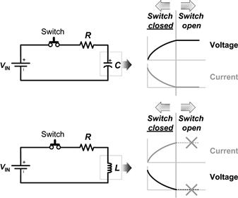
Figure 1.3: Basic charging/discharging circuits for capacitor and inductor.
Note that here we are using a mechanical switch for the sake of simplicity, thus also assuming it has none of the parasitics we talked about earlier. At time t=0, we close the switch (ON) and thus apply the DC voltage supply (VIN) across the capacitor (C) through the small series limiting resistor (R). What happens?
Most people get this right. The capacitor voltage increases according to the well-known exponential curve VIN×(1−e−t/τ), with a “time constant” of τ=RC. The capacitor current, on the other hand, starts from a high initial value of VIN/R and then decays exponentially according to (VIN/R)×e−t/τ. Yes, if we wait “a very long time,” the capacitor would get charged up almost fully to the applied voltage VIN, and the current would correspondingly fall (almost) to zero. Let us now open the switch (OFF), though not necessarily having waited a very long time. In doing so, we are essentially attempting to force the current to zero (that is what a series switch is always supposed to do). What happens? The capacitor remains charged to whatever voltage it had already reached, and its current goes down immediately to zero (if not already there).
Now let us repeat the same experiment, but with the capacitor replaced by an inductor (L), as also shown in Figure 1.3. Interviewees usually get the “charging” part (switch-closed phase) of this question right too. They are quick to point out that the current in the inductor behaves just as the voltage across the capacitor did during the charging phase. And the voltage across the inductor decays exponentially, just as the capacitor current did. They also seem to know that the time constant here is τ=L/R, not RC.
This is actually quite encouraging, as it seems we have, after all, heard of the “duality principle.” In simple terms this principle says that a capacitor can be considered as an inverse (or “mirror”) of an inductor because the voltage–current equations of the two devices can be transformed into one another by exchanging the voltage and current terms. So, in essence, capacitors are analogous to inductors, and voltage to current.
But wait! Why are we even interested in this exotic-sounding new principle? Don’t we have enough on our hands already? Well, it so happens, that by using the duality principle we can often derive a lot of clues about any L-based circuit from a C-based circuit, and vice versa — right off the bat — without having to plunge headlong into a web of hopelessly non-intuitive equations. So, in fact, we would do well to try to use the duality principle to our advantage if possible.
With the duality principle in mind, let us attempt to open the switch in the inductor circuit and try to predict the outcome. What happens? No! Unfortunately, things don’t remain almost “unchanged” as they did for a capacitor. In fact, the behavior of the inductor during the off-phase is really no replica of the off-phase of the capacitor circuit.
So does that mean we need to jettison our precious duality principle altogether? Actually we don’t. The problem here is that the two circuits in Figure 1.3, despite being deceptively similar, are really not duals of each other. And for that reason, we really can’t use them to derive any clues either. A little later, we will construct proper dual circuits. But for now we may have already started to suspect that we really don’t understand inductors as well as we thought, nor in fact the duality principle we were perhaps counting on to do so.
The Law of Conservation of Energy
If a nervous interviewee hazards the guess that the current in the inductor simply “goes to zero immediately” on opening the switch, a gentle reminder of what we all learnt in high school is probably due. The stored energy in a capacitor is CV2/2, and so there is really no problem opening the switch in the capacitor circuit — the capacitor just continues to hold its stored energy (and voltage). But in an inductor, the stored energy is LI2/2. Therefore, if we speculate that the current in the inductor circuit is at some finite value before the switch is opened and zero immediately afterward, the question arises: to where did all the stored inductor energy suddenly disappear? Hint: we have all heard of the law of conservation of energy — energy can change its form, but it just cannot be wished away!
Yes, sometimes a particularly intrepid interviewee will suggest that the inductor current “decays exponentially to zero” on opening the switch. So the question arises — where is the current in the inductor flowing to and from? We always need a closed galvanic path for current to flow (from Kirchhoff’s laws)!
But, wait! Do we even fully understand the charging phase of the inductor well enough? Now this is getting really troubling! Let’s find out for ourselves!
The Charging Phase and the Concept of Induced Voltage
From an intuitive viewpoint, most engineers are quite comfortable with the mental picture they have acquired over time of a capacitor being charged — the accumulated charge keeps trying to repel any charge trying to climb aboard the capacitor plates till finally a balance is reached and the incoming charge (current) gets reduced to near-zero. This picture is also intuitively reassuring because at the back of our minds, we realize it corresponds closely with our understanding of real-life situations — like that of an overcrowded bus during rush hour, where the number of commuters that manage to get on board at a stop depends on the capacity of the bus (double-decker or otherwise) and also on the sheer desperation of the commuters (the applied voltage).
But coming to the inductor charging circuit (i.e., switch closed), we can’t seem to connect this too readily to any of our immediate real-life experiences. Our basic question here is — why does the charging current in the inductor circuit actually increase with time? Or equivalently, what prevents the current from being high to start with? We know there is no mutually repelling “charge” here, as in the case of the capacitor. So why?
We can also ask an even more basic question — why is there any voltage even present across the inductor? We always accept a voltage across a resistor without argument — because we know Ohm’s law (V=I×R) all too well. But an inductor has (almost) no resistance — it is basically just a length of solid conducting copper wire (wound on a certain core). So how does it manage to “hold-off” any voltage across it? In fact, we are comfortable about the fact that a capacitor can hold voltage across it. But for the inductor — we are not very clear! Further, if what we have learnt in school is true — that electric field by definition is the voltage gradient dV/dx (“x” being the distance), we are now faced with having to explain a mysterious electric field somewhere inside the inductor! Where did that come from?
It turns out that, according to Lenz and/or Faraday, the current takes time to build up in an inductor only because of “induced voltage.” This voltage, by definition, opposes any external effort to change the existing flux (or current) in an inductor. So, if the current is fixed, yes, there is no voltage present across the inductor — it then behaves just as a piece of conducting wire. But the moment we try to change the current, we get an induced voltage across it. By definition, the voltage measured across an inductor at any moment (whether the switch is open or closed, as in Figure 1.3) is the “induced voltage.”
Note: We also observe that the analogy between a capacitor/inductor and voltage/current, as invoked by the duality principle, doesn’t stop right there! For example, it was considered equally puzzling at some point in history, how at all any current was apparently managing to flow through a capacitor — when the applied voltage across it was changed. Keeping in mind that a capacitor is basically two metal plates with an interposing (nonconducting) insulator, it seemed contrary to the very understanding of what an “insulator” was supposed to be. This phenomenon was ultimately explained in terms of a “displacement current” that flows (or rather seems to flow) through the plates of the capacitor when the voltage changes. In fact, this current is completely analogous to the concept of “induced voltage” — to explain the fact that a voltage was being observed across an inductor when the current through it was changing.
So let us now try to figure out exactly how the induced voltage behaves when the switch is closed. Looking at the inductor charging phase in Figure 1.3, the inductor current is initially zero. Thereafter, by closing the switch, we are attempting to cause a sudden change in the current. The induced voltage now steps in to try to keep the current down to its initial value (zero). So we apply “Kirchhoff’s voltage law” to the closed loop in question. Therefore, at the moment the switch closes, the induced voltage must be exactly equal to the applied voltage, since the voltage drop across the series resistance R is initially zero (by Ohm’s law).
As time progresses, we can think intuitively in terms of the applied voltage “winning.” This causes the current to rise up progressively. But that also causes the voltage drop across R to increase, and so the induced voltage must fall by the same amount (to remain faithful to Kirchhoff’s voltage law). That tells us exactly what the induced voltage (voltage across inductor) is during the entire switch-closed phase.
Why does the applied voltage “win”? For a moment, let’s suppose it didn’t. That would mean the applied voltage and the induced voltage have managed to completely counterbalance each other — and the current would then remain at zero (or constant). However, that cannot be because zero rate of change in current implies no induced voltage either! In other words, the very existence of induced voltage depends on the fact that current changes, and it must change.
We also observe rather thankfully that all the laws of nature bear each other out. There is no contradiction whichever way we look at the situation. For example, even though the current in the inductor is subsequently higher, its rate of change is less, and therefore, so is the induced voltage (on the basis of Faraday’s/Lenz’s law). And this “allows” for the additional drop appearing across the resistor, as per Kirchhoff’s voltage law!
But we still don’t know how the induced voltage behaves when the switch turns OFF! To unravel this part of the puzzle, we actually need some more analysis.
The Effect of the Series Resistance on the Time Constant
Let us ask — what are the final levels at the end of the charging phase in Figure 1.3 — that is, of the current in the inductor and the voltage across the capacitor. This requires us to focus on the exact role being played by R. Intuitively, we expect that for the capacitor circuit, increasing the R will increase the charging time constant τ. This is borne out by the equation τ=RC too, and is what happens in reality too. But for the inductor charging circuit, we are again up against another seemingly counter-intuitive behavior — increasing R actually decreases the charging time constant. That is in fact indicated by τ=L/R too.
Let us attempt to explain all this. Looking at Figure 1.4 which shows the inductor charging current, we can see that the R=1 Ω current curve does, indeed, rise faster than the R=2 Ω curve (as intuitively expected). But the final value of the R=1 Ω curve is twice as high. Since by definition, the time constant is “the time to get to 63% of the final value,” the R=1 Ω curve has a larger time constant, despite the fact that it did rise much faster from the get-go. So, that explains the inductor current waveforms.
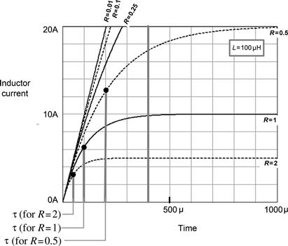
Figure 1.4: Inductor current during charging phase for different R (in ohms), for an applied input of 10 V.
But looking at the inductor voltage waveforms in Figure 1.5, we see there is still some explaining to do. Note that for a decaying exponential curve, the time constant is defined as the time it takes to get to 37% of the initial value. So, in this case, we see that though the initial values of all the curves are the same, yet, for example, the R=1 Ω curve has a slower decay (larger time constant) than the R=2 Ω curve! There is actually no mystery involved here, since we already know what the current is doing during this time (Figure 1.4), and therefore the voltage curves follow automatically from Kirchhoff’s laws.
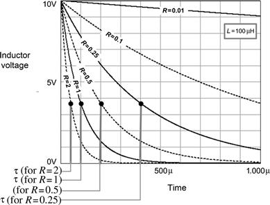
Figure 1.5: Inductor voltage during charging phase for different R (in ohms), for an applied input of 10 V.
The conclusion is that if, in general, we ever make the mistake of looking only at an inductor voltage waveform, we may find ourselves continually baffled by an inductor! For an inductor, we should always try to see what the current in it is trying to do. That is why, as we just found out, the voltage during the off-time is determined entirely by the current. The voltage just follows the dictates of the current, not the other way around. In fact, in Chapter 8, we will see how this particular behavioral aspect of an inductor determines the exact shape of the voltage and current waveforms during a switch transition and thereby determines the crossover (transition) loss too.
The Inductor Charging Circuit with R=0 and the “Inductor Equation”
What happens if R is made to decrease to zero?
From Figure 1.5, we can correctly guess that the only reason that the voltage across the inductor during the on-time changes at all from its initial value VIN is the presence of R! So if R is 0, we can expect that the voltage across the inductor never changes during the on-time! The induced voltage must then be equal to the applied DC voltage. That is not strange at all — if we look at it from the point of view of Kirchhoff’s voltage law, there is no voltage drop present across the resistor — simply because there is no resistor! So in this case, all the applied voltage appears across the inductor. And we know it can “hold-off” this applied voltage, provided the current in it is changing. Alternatively, if any voltage is present across an inductor, the current through it must be changing!
So now, as suggested by the low-R curves of Figures 1.4 and 1.5, we expect that the inductor current will keep ramping up with a constant slope during the on-time. Eventually, it will reach an infinite value (in theory). In fact, this can be mathematically proven by differentiating the inductor charging current equation with respect to time, and then putting R=0 as follows:
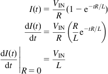
So, we see that when the inductor is connected directly across a voltage source VIN, the slope of the line representing the inductor current is constant and equal to VIN/L (the current rising constantly).
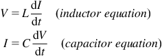
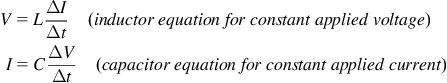
Note that in the above derivation, the voltage across the inductor happened to be equal to VIN because R was 0. But in general, if we call “V” the voltage actually present across the inductor (at any given moment), I being the current through it, we get the general “inductor equation”
![]()
This equation applies to an ideal inductor (R=0), in any circuit, under any condition. For example, it not only applies to the “charging” phase of the inductor, but also applies to its “discharging” phase!
Note: When working with the inductor equation, for simplicity, we usually plug in only the magnitudes of all the quantities involved (though we do mentally keep track of what is really happening, i.e., current rising or falling).
The Duality Principle
We now know how the voltage and current (rather its rate of change) are mutually related in an inductor during both the charging and discharging phases. Let us use this information, along with a more complete statement of the duality principle, to finally understand what really happens when we try to interrupt the current in an inductor.
The principle of duality concerns the transformation between two apparently different circuits, which have similar properties when current and voltage are interchanged. Duality transformations are applicable to planar circuits only and involve a topological conversion: capacitor and inductor interchange, resistance and conductance interchange, and voltage source and current source interchange.
We can thus spot our “mistakes” in Figure 1.3. First, we were using an input voltage source applied to both circuits — whereas we should have used a current source for the “other” circuit. Second, we used a series switch in both the circuits. We note that the primary function of a series switch is only to interrupt the flow of current — not to change the voltage (though that may happen as a result). So, if we really want to create proper mirror (dual) circuits, then forcing the current to zero in the inductor is the dual of forcing the voltage across the capacitor to zero. And to implement that, we obviously need to place a switch in parallel to the capacitor (not in series with it). With these changes in mind, we have finally created true dual circuits as shown in Figure 1.6 (both are actually equally impractical in reality!).
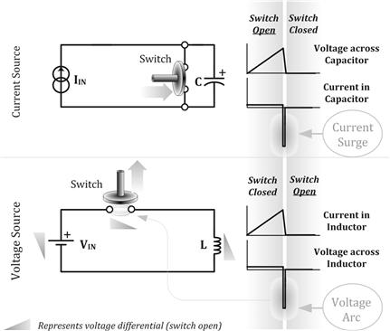
Figure 1.6: Mirror circuits for understanding inductor discharge.
The “Capacitor Equation”
To analyze what happens in Figure 1.6, we must first learn the “capacitor equation” — analogous to the “inductor equation” derived previously. If the duality principle is correct, both the following equations must be valid:
Further, if we are dealing with “straight-line segments” (constant V for an inductor and constant I for a capacitor), we can write the above equations in terms of the corresponding increments or decrements during the given time segment.
It is interesting to observe that the duality principle is actually helping us understand how the capacitor behaves when being charged (or discharged) by a current source. We can guess that the voltage across the capacitor will then ramp up in a straight line — to near infinite values — just as the inductor current does with an applied voltage source. And in both cases, the final values reached (of the voltage across the capacitor and the current through the inductor) are dictated only by various parasitics that we have not considered here — mainly the ESR of the capacitor and the DCR of the inductor respectively.
The Inductor Discharge Phase
We now analyze the mirror circuits of Figure 1.6 in more detail.
We know intuitively (and also from the capacitor equation) what happens to a capacitor when we attempt to suddenly discharge it (by means of the parallel switch). Therefore, we can now easily guess what happens when we suddenly try to “discharge” the inductor (i.e., force its current to zero by means of the series switch).
We know that if a “short” is applied across any capacitor terminals, we get an extremely high-current surge for a brief moment — during which time the capacitor discharges and the voltage across it ramps down steeply to zero. So, we can correctly infer that if we try to interrupt the current through an inductor, we will get a very high voltage across it — with the current simultaneously ramping down steeply to zero. So the mystery of the inductor “discharge” phase is solved — with the help of the duality principle!
But we still don’t know exactly what the actual magnitude of the voltage spike appearing across the switch/inductor is. That is simple — as we said previously, during the off-time, the voltage will take on any value to force current continuity. So, a brief arc will appear across the contacts as we try to pull them apart (see Figure 1.6). If the contacts are separated by a greater distance, the voltage will increase automatically to maintain the spark. And during this time, the current will ramp down steeply. The arcing will last for as long as there is any remaining inductor stored energy — that is, till the current completely ramps down to zero. The rate of fall of current is simply V/L, from the inductor equation. So eventually, all the stored energy in the inductor is completely dissipated in the resulting flash of heat and light, and the current returns to zero simultaneously. At this moment, the induced voltage collapses to zero too, its purpose complete. This is in fact the basic principle behind the automotive spark plug, and the camera flash too (occurring in a more controlled fashion).
But wait — we have stated above that the rate of fall of current in the inductor circuit was “V/L.” What is V? V is the voltage across the inductor, not the voltage across the contacts. In the following sections, we will learn that the voltage across an inductor (almost always) reverses when we try to interrupt its current. If that is true, then by Kirchhoff’s voltage law, since the algebraic sum of all the voltage drops in any closed circuit must add up to zero, the voltage across the contacts will be equal to the sum of the magnitudes of the induced voltage and the applied DC rail — however, the sign of the voltage across the contacts (i.e., its direction) will necessarily be opposite to the other voltages (see the gray triangles in the lower schematic of Figure 1.6). Therefore, we conclude that the magnitude of the voltage spike across the inductor is equal to the magnitude of the voltage across the contacts minus the magnitude of the input DC voltage.
Finally, we know everything about the puzzling inductor discharge phase!
Flyback Energy and Freewheeling Current
The energy that “must get out” of the inductor when we try to open the switch is called the “flyback” energy. The current that continues to force its way through is called the “freewheeling” current. Note that this not only sounds, but, in fact, is very similar to another real-world situation — that of a mechanical spinning wheel or of a “flywheel.” In fact, understanding the flywheel can help greatly in gaining an intuitive insight into the behavior of an inductor.
Just as the inductor has stored energy related to the current flowing through it, the flywheel stores energy related to its spinning action. And neither of these energy terms can be wished away in an instant. In the case of the flywheel, we can apply “brakes” to dissipate its rotational energy (as heat in the brake linings) — and we know this will produce a progressive reduction in the spinning. Further, if the brakes are applied more emphatically, the time that will elapse till the spinning stops entirely gets proportionately decreased. That is very similar to an inductor — with the induced voltage (during the off-time) playing the part of the “brakes” and the current being akin to the spinning. So, the induced voltage causes a progressive reduction in the current. If we have a higher induced voltage, this will cause a steeper fall in the current. In fact, that is also indicated by the inductor equation V=LdI/dt!
However, we have also learned something more fundamental about the behavior of an inductor, as described next.
Current Must Be Continuous, Its Slope Need Not Be
The keyword in the previous section was progressive. From a completely mathematical/geometrical point of view now, we should understand that any curve representing inductor current cannot be discontinuous (no sudden jumps allowed) — because that will in effect cause energy to be discontinuous, which we know is impossible. But we can certainly cause the slope of the current (i.e., its dI/dt) to have “jumps.” So we can, for example, change the slope of current (dI/dt) in an instant — from one representing a rising ramp (increasing stored energy) to one representing a falling ramp (opposite sign, i.e., decreasing energy). However, the current itself must always be continuous. This is shown in Figure 1.7 under the choices marked “possible.”
Figure 1.7: Inductor current must be continuous, but its slope need not be. Capacitor voltage must be continuous, but its slope need not be.
Note that there are two options in the figure that are “possible.” Both are so, simply because they do not violate any known physical laws. However, one of these choices is considered “unacceptable” because of the huge spike — which we know can damage the switch. The other choice, marked “acceptable,” is in fact what really happens in any switching converter topology, as we will soon see.
The Voltage Reversal Phenomenon
We mentioned there is a voltage reversal across the switch when we try to interrupt its current. Let us try to understand that better now.
An intuitive (but not necessarily rigorous) way to visualize it is shown in Figure 1.8. Here we note that when the switch is closed (upper schematic), the current is shown leaving the positive terminal of the applied DC voltage source — that being the normal convention for describing the direction of current flow. During this on-time, the upper end of the inductor gets set to a higher voltage than its lower end. Subsequently, when the switch opens, the input DC source gets disconnected from the inductor. But we have just learnt that the current demands to keep flowing (at least for a while) — in the same direction as previously flowing. So during the switch off-time, we can mentally visualize the inductor as becoming a sort of “voltage source,” forcing the current to keep flowing. For that reason, we have placed an imaginary (gray) voltage source (battery symbol) across the inductor in the lower half of the figure — its polarity in accordance with the convention that current must leave by the positive terminal of any voltage source. Thus, we can see that this causes the lower end of the inductor to now be at a higher voltage than its upper end. Clearly, voltage reversal has occurred — simply by the need to maintain current continuity.
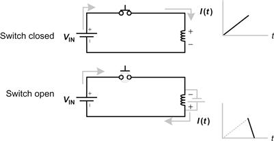
Figure 1.8: How the voltage reverses on attempted interruption of inductor current.
The phenomena of voltage reversal can be traced back to the fact that induced voltage always opposes any change (in current). However, in fact, voltage reversal does not always occur. For example, voltage reversal does not occur during the initial startup (“power-up”) phase of a Boost converter. That is because the primary requirement is only that the inductor current somehow needs to keep flowing — voltage takes a backseat. So hypothetically, if a circuit is wired in a certain way, and the conditions are “right,” it is certainly possible that voltage reversal won’t occur, so long as current continuity can still be maintained.
However, we must be clear that if and when a converter reaches a “steady state,” voltage reversal will necessarily occur at every switch transition.
For that we now have to understand what a “steady state” is.
A Steady State in Power Conversion and the Different Operating Modes
A steady state is, as the name indicates, stable. So, it is in essence the opposite of a runaway or unstable condition. But we can easily visualize that we will in fact get an unstable condition if at the end of every cycle, we don’t return to the current we started the cycle with — because then, every successive cycle, we will accumulate a net increase or decrease of current, and the situation will keep changing forever (in theory).
From V=LΔI/Δt, it is clear that if the current is ramping up for a positive (i.e., applied) voltage, the current must ramp down if the voltage reverses. So the following equations must apply (magnitudes only):
Here the subscript “ON” refers to the switch being closed and “OFF” refers to the switch being open. VON and VOFF are the respective voltages across the inductor during the durations ΔtON and ΔtOFF. Note that very often, ΔtON is written simply as “tON,” the switch on-time. And similarly, ΔtOFF is simply “tOFF,” the switch off-time.
Now suppose we are able to create a circuit in which the amount the current ramps up by in the on-time (ΔION) is exactly equal to the amount the current ramps down by during the off-time (ΔIOFF). If that happens, we would have reached a steady state. Now we could repeat the same sequence an innumerable amount of times, and get the same result each and every time. In other words, every “switching cycle” would then be an exact replica of the previous cycle. Further, we could also perhaps get our circuit to deliver a steady stream of (identical) energy packets continuously to an output capacitor and load. If we could do that, by definition, we would have created a power converter!
Achieving a steady state is luckily not as hard as it may sound. Nature automatically tries to help every natural process move toward a stable state (without “user intervention”). So, in our case, all we need to do on our part is to provide a circuit that allows these conditions to develop naturally (over several cycles). And if we have created the right conditions, a steady state will ultimately result. Further, this would be self-sustaining thereafter. Such a circuit would then be called a switching “topology”!
Conversely, any valid topology must be able to reach a state described by the following key equation ΔION=ΔIOFF≡ΔI. If it can’t get this to happen, it is not a topology. Therefore, this simple current increment/decrement equation forms the litmus test for validating any new switching topology.
Note that the inductor equation, and thereby the definition of “steady state,” refers only to the increase/decrease in current — it says nothing about the actual (absolute) value of the current at the start (and end) of every cycle. So, there are in fact several possibilities. We could have a steady state in which the current returns to zero every cycle, and this is called a “discontinuous conduction mode” (DCM). However, if the current stays pegged at some non-zero value throughout, we will have “continuous conduction mode” (CCM). The latter mode is the most common mode of operation encountered in power conversion. In Figure 1.9, we have graphically shown these operating modes (all in steady state). We also have some other modes that we will talk about very soon. Note that in the figure, the “square” waveform is the voltage across the inductor and the slowly ramping waveform is the inductor current. Let us make some related observations:
a. We see that the voltage across the inductor always reverses at every switching event (as expected in steady state).
b. We note that since the inductor equation relates voltage to the slope of the current, not to the actual current, therefore, for a given VON and VOFF, several current waveforms are possible (all having the same dI/dt for corresponding segments). Each of these possibilities has a name — CCM, DCM, BCM (boundary conduction mode, also called critical conduction mode), and so on. Which of these operating modes actually occurs depends on the specific circuit (i.e., the topology) and also the application conditions (how much output power we are demanding and what the input and output voltages are).
c. The inductor voltages, VON and VOFF shown in the figure, are related to the application conditions VIN and/or VO. Their exact relationship will become known a little later, and we will also learn that it depends on the specific topology.
d. A key question is — what is the exact relationship between the average inductor current and the load current? We will soon see that that too depends on the specific topology. However, in all cases, the average inductor current (“IAVG” or “IL”) is proportional to the load current (“IO”). So if, for example, IO is 2 A and IAVG is 10 A, then if IO is decreased to 1 A, IAVG will fall to 5 A. Therefore on decreasing the load current, we can get IAVG to decrease, as indicated in Figure 1.9.
e. Typically, we transit automatically from CCM to DCM, just by reducing the load current of the converter. But note that we will necessarily have to pass through BCM along the way.
f. “BCM” is just that — a “boundary conduction mode” — situated exactly between CCM and DCM. It is therefore a purely philosophical question to ask whether BCM should be viewed as CCM or DCM (at their respective extremes) — it really doesn’t matter.
g. Note that in all the cases shown in Figure 1.9, with the exception of DCM, the average inductor current IAVG is just the geometrical center of the ramp part of the current waveform. In DCM, however, we have an additional interval in which there is no current passing for a while. So, to find the average value of the inductor current, a rather more detailed calculation is required. In fact, that is the primary reason why DCM equations turn out looking so complicated — to the point that many engineers seem to rather instinctively ignore DCM altogether, despite some advantages of operating a converter in DCM instead of CCM.
Note: Expectedly, all DCM equations lead to exactly the same numerical results as the CCM equations — when the converter is in BCM. Practically speaking, we can freely pick and choose whether to use the CCM equations, or the more formidable-looking DCM equations, for evaluating a converter in BCM. Of course, there is no reason why we would ever want to struggle through complicated equations, when we can use much simpler equations to get the same results!
h. What really is the average inductor current “IAVG” as shown in Figure 1.9? A nice way to understand this parameter is through the “car analogy.” Suppose we press the gas pedal of a car. The car responds by increasing its speed. In an analogous fashion, when we apply a voltage across an inductor (the on-time voltage “VON”), the current ramps up. Subsequently, suppose we press on the brakes of the car. The car will then respond by decreasing its speed. Similarly, when the applied voltage is removed from the inductor, voltage reversal occurs, and an induced voltage (the “brakes”) appears across the inductor “VOFF.” Since it is in the opposite direction as VON, it causes the current to ramp down. So now, if we press the gas pedal (VON), followed by the brakes (VOFF), in quick succession, and with the right timing, we could still make the car continue to move forward despite the constant lurching. It would then have a certain average speed — depending on the ratio of the gas pedal duration and the subsequent braking duration. In power conversion, this “lurching” is analogous to the “current ripple” ΔI=ΔION=ΔIOFF. And quite similarly, we have an “average inductor current” IAVG too, as shown in Figure 1.9. However, we do understand that in a power converter, the output capacitor eventually absorbs (or smoothens) this “lurching” and thus manages to deliver a steady DC current to the load as desired.
i. Some control ICs manage to maintain the converter in BCM mode under all application conditions. Examples of these are certain types of “hysteretic controllers” and self-oscillating types called “ringing choke converters” (RCCs). However, we know that the current ramps down at a rate V/L. And since V depends on the input/output voltages, the time to get to zero current depends on the specific application conditions. Therefore, in any BCM implementation, we always lose the advantage of fixed switching frequency operation.
j. Most conventional topologies are nowadays labeled “non-synchronous” — to distinguish them from more recent “synchronous” topologies. In the former, a diode is always present (the catch diode) that prevents the inductor current from reversing direction any time during the switching cycle. That is why, on reducing output power and/or increasing input voltage, we automatically transit from CCM to DCM. However, in synchronous topologies, the catch diode is either replaced completely by, or supplemented with, a low-drop MOSFET placed across it. So, whenever the diode is supposed to conduct, we force this extra MOSFET into conduction for that duration. Since the drop across this MOSFET is much lower than across a diode, not only do we manage to significantly reduce the conduction loss in the freewheeling path, but we can also now allow reverse inductor current — that is, current moving instantaneously away from the load. However, note that the average inductor current could still be positive — see Figure 1.9. Further, with negative currents now being “allowed,” we no longer get DCM on reducing output power, but rather enter FPWM/FCCM (forced continuous conduction mode) as described in the figure.
Note: It is fortunate that almost all the standard CCM design equations (for non-synchronous topologies) apply equally to FCCM. So from the viewpoint of a harried designer, one of the “advantages” of using synchronous topologies is that the complicated DCM equations are a thing of the past! However, there are some new complications and nuances of synchronous topologies that we need to understand eventually.
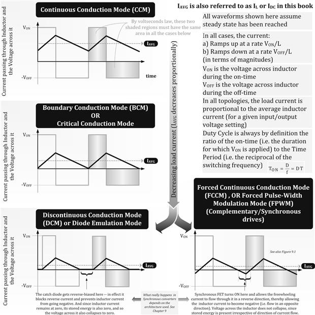
Figure 1.9: Different operating modes of switching regulators.
The Voltseconds Law, Inductor Reset and Converter Duty Cycle
There is another way to describe a steady state, by bringing in the inductor equation V=LΔI/Δt.
We know that during a steady state ΔION=ΔIOFF≡ΔI. So what we are also saying is that
in steady state, the product of the voltage applied across the inductor, multiplied by the duration we apply it for (i.e., the on-time), must be equal to the voltage that appears across the inductor during the off-time, multiplied by the duration that it lasts for.
Therefore, we get
![]()
The product of the voltage and the time for which it appears across the inductor is called the “voltseconds” across the inductor. So equivalently, what we are also saying is that
if we have an inductor in a steady state, the voltseconds present across it during the on-time (i.e., current ramp-up phase) must be exactly equal in magnitude, though opposite in sign, to the voltseconds present across it during the off-time (i.e., during the current ramp-down phase).
That also means that if we plot the inductor voltage versus time, the area under the voltage curve during the on-time must be equal to the area under the voltage curve during the off-time. But we also know that voltage reversal always occurs in steady state. So clearly, these two areas must have the opposite signs. See the shaded segments in Figure 1.9.
Therefore, we can also say that the net area under the voltage curve of an inductor must be equal to zero (in any switching cycle under steady state operation).
Note that since the typical times involved in modern switching power conversion are so small, “voltseconds” turns out to be a very small number. Therefore, to make numbers more manageable, we usually prefer to talk in terms of “Et” or the “voltμseconds.” Et is clearly just the voltage applied across the inductor multiplied by the time in microseconds (not seconds). Further, we know that typical inductance values used in power conversion are also better expressed in terms of “μΗ” (microhenrys), not H. So, from V=Ldl/dt we can write
![]()
or simply
![]()
Note: If in any given equation Et and L appear together , it should be generally assumed that L is in μΗ. Similarly, if we are using voltseconds, that would usually imply L is in H (unless otherwise indicated).
Another term often used in power, one that tells us that we have managed to return to the same inductor current (and energy) that we started off with, is called inductor “reset.” Reset occurs at the very moment when the equality ΔIOFF=ΔION is established. Of course, we could also have a nonrepetitive (or “single-shot”) event, where the current starts at zero and then returns to zero — and that too would be inductor “reset.”
The corollary is that in a repetitive switching scenario (steady state), an inductor must be able to reset every cycle. Reversing the argument — any circuit configuration that makes inductor reset an impossibility — is not a viable switching topology.
When we switch repetitively at a switching frequency “f,” the “time period” (T) is equal to 1/f. We can also define the “duty cycle” (D) of a power converter as the ratio of the on-time of the switch to the time period. So,
![]()
Note that we can also write this as
![]()
At this point, we should be very clear how we are defining “tOFF” in particular. While applying the voltseconds law, we had implicitly assumed that tOFF was the time for which the induced voltage VOFF lasts, not necessarily the time for which the switch is OFF (i.e., T−tON). In DCM, they are not the same (see Figure 1.9)! Only in CCM do we get
![]()
and therefore
![]()
If working in DCM, we should stick to the more general definition of duty cycle given initially.
Using and Protecting Semiconductor Switches
We realize that all topologies exist only because they can achieve a steady state. In an “experimental” topology in which we can’t make ΔION=ΔIOFF happen, the inductor may see a net increase of current every cycle, and this can eventually escalate to a very large, almost uncontrolled value of current in just a few cycles. The name given to this progressive ramping-up (or down) of current (or inductor energy), one that is ultimately limited only by parasitics like the ESR and DCR, is called “staircasing.” The switch will also turn ON into the same current and can thus be destroyed — that is if the induced voltage spike hasn’t already done so (which can happen, if the situation is anything similar to the “unacceptable” plots shown in Figure 1.7!).
Note: The very use of the inductor equation V=LdI/dt actually implies we are ignoring its parasitic resistance, DCR. The inductor equation is an idealization, applying only to a “perfect” inductor. That is why we had to put R=0 when we derived it previously.
In an actual power supply, the “mechanical switch” is replaced with a modern semiconductor device (like the MOSFET) — largely because then the switching action can be implemented reliably and also at a very high repetition rate. But semiconductor devices have certain electrical ratings that we need to be well aware of.
Every semiconductor device has an “absolute maximum voltage rating” that, unlike any typical mechanical relay, cannot be exceeded even momentarily — without possibly causing its immediate destruction. So, most MOSFETs do not allow any “latitude” whatsoever in terms of their voltage ratings.
Note: There are some “avalanche-rated” MOSFETs available, which can internally “clamp” the excess voltage appearing across them to some extent. In doing so, they are basically dissipating the excess energy associated with the voltage spike, within their internal clamp. Therefore, they can survive a certain amount of excess voltage (and energy), but only for a short duration (since the device heats up quickly).
There is also a maximum semiconductor device “current rating,” but that is usually more long term in nature, dictated by the comparatively slower process of internal heat build-up inside the device. So hypothetically speaking, we could perhaps exceed the current rating somewhat, though only for a short time. Of course, we don’t want to run a device constantly in this excess-current condition. However, under “abnormal conditions,” like an “overload” on the output of the converter (or the extreme case of a shorted output), we may judiciously allow for a certain amount of “temporary/transient abuse” with regard to the current rating — but certainly not with the absolute maximum voltage rating!
In a practical implementation, we have to design the converter, select the switch, and then lay it all out on a PCB with great care — to ensure in particular that there is no voltage spike that can “kill” the switch (or other semiconductor devices present on the board). Occasionally, we may therefore need to add an external “snubber” or “clamp” across the switch so as to truncate any remnant spikes to within the voltage ratings of the switch.
To protect the switch (and converter) from excess currents, a “current limit” is usually required. In this case, the current in the inductor, or in the switch, is sensed, and then compared against a set threshold. If and when that is momentarily exceeded, the control circuitry forces the switch to turn OFF immediately for the remainder of the switching cycle so as to protect itself. In the next cycle, no “memory” is usually retained of what may have happened in the preceding cycle. Therefore, every switching cycle is started “afresh,” with the current being continuously monitored to ensure it is at a “safe” level. If not, protective action is again initiated and can be repeated every cycle for several cycles if necessary, until the “overcurrent” condition ceases.
Note: One of the best known examples of the perils of “previous-cycle memory” in implementing current limit occurs in the popular “Simple Switcher®” family of parts (at www.national.com). In the “third-generation” LM267x family, the control circuit rather surprisingly reduces the duty cycle to about 45% for several cycles after any single current limit event. It then tries to progressively allow the duty cycle to increase over several successive cycles back to its required value. But this causes severe output “foldback” and consequent inability to regulate up to full rated load, particularly in applications that require a duty cycle greater than 50%. This condition is further exacerbated with large-output capacitances because the higher currents required to charge the output capacitor after the removal of an abnormal condition (e.g., output short) can lead to another current limit event (and consequent foldback for several cycles again) — before the duty cycle has been able to return to its desired value. In effect, the converter goes into a continuous “motorboating” condition on removal of the output short, and so the output never recovers. This is rather obliquely “revealed” only deep within the product datasheets under the intriguing heading “Additional Applications Information.”
With the introduction to power conversion now complete, we turn our attention to how switching topologies develop naturally out of the behavior of an inductor.
Evolution of Switching Topologies
Controlling the Induced Voltage Spike by Diversion through a Diode
We realize that our “problem” with using an inductor is two-fold: either we are going to end up with near-infinite induced voltage spikes, as shown in Figures 1.6 and 1.7, or if we do somehow manage to control the induced voltage to some finite level, the equation V=LdI/dt tells us we could very well end up with near-infinite currents (staircasing).
And further, coming to think of it, our basic purpose is still not close to being fulfilled — we still don’t know how to derive any useful power from our circuit!
Luckily, all the above-described problems can be solved in one stroke! And in doing so, we will arrive at our very first “switching topology.” Let’s now see how that comes about.
We recollect from Figure 1.6 that the spike of induced voltage at switch turn-off occurs only because the current (previously flowing in the inductor) was still demanding a path along which to flow — and somehow unknowingly, we had failed to provide any. Therefore, nature, in search of the “weakest link,” found this in the switch itself — and produced an arc across it to try to move the current across anyway.
But suppose we consciously provide a “diversionary path.” Then there would be no problem turning the switch OFF and stopping the inductor current flowing through the switch — because it could continue to flow via this alternate route. The inductor would then no longer “complain” in the form of a dangerous voltage spike. Thereafter, perhaps we can even reroute the current back into the switch when it turns ON again. Finally, we can perhaps even repeat the ON–OFF–ON–OFF process indefinitely at a certain switching frequency.
In Figure 1.10, we have created such an alternate path. We will see that the way the diode is pointed, this path can come into play automatically, and only when the switch turns OFF.
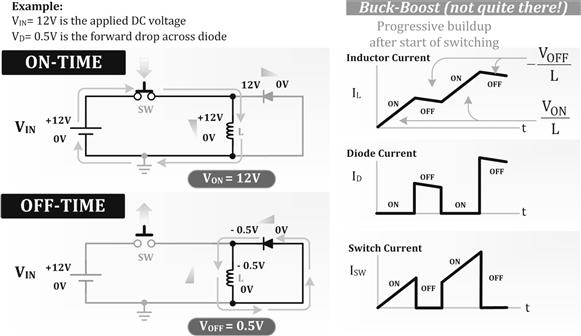
Figure 1.10: Providing a “diversion” for the inductor current through a diode.
Just to make things clearer, we have used some sample numbers in Figure 1.10. We have taken the applied input voltage to be 12 V and assumed a typical Schottky diode forward drop of 0.5 V. Note that we are assuming a “perfect” switch here (no forward drop), for the sake of simplicity. We make the following observations:
• When the switch is ON (closed), the voltage at the upper end of the inductor L is at 12 V and the lower end is at 0 V (“ground”). So the diode is reverse-biased and does not conduct. Energy is then being built up in the inductor by the applied DC voltage source.
The magnitude of the voltage applied across the inductor during the on-time of the switch (i.e., “VON”) is equal to 12 V.
• When the switch turns OFF (open), an alternate path is available for the inductor current to flow — through the diode. And we can be sure that “nature” (in our case the “induced voltage”) will attempt to exploit this path — by forcing the diode to conduct. But for that, the diode must get “forward-biased,” that is, its anode must get to a voltage 0.5 V higher than the cathode. But the anode is being held at ground (0-V rail). Therefore, the cathode must fall to –0.5 V.
The magnitude of the voltage applied across the inductor during the off-time of the switch (i.e., “VOFF”) is equal to 0.5 V.
• Note that the induced voltage during the switch off-time has had its polarity reversed.
• The rate of rise of the current (in the inductor and switch) during the on-time is equal to VON/L. And during the off-time, the current ramps down (much more slowly), at a rate of VOFF/L (in the inductor and diode).
• Yes, if we wait long enough, the inductor current will finally ramp down to zero (inductor “reset”). But if we don’t wait and turn the switch back ON again, the current will again start to ramp up (staircasing), as shown in Figure 1.10.
• Note that both the switch and the diode currents have a “choppy” waveform — since one takes over where the other left off. This is in fact always true for any switching power converter (or topology).
Summarizing: We see that having provided a diversionary path for the current, the inductor isn’t “complaining” anymore and there is no uncontrolled induced voltage spike anymore. But we certainly have now ended up with a possible problem of escalating currents. And come to think of it, neither do we have a useful output rail yet, which is what we are basically looking to do finally. In fact, all that we are accomplishing in Figure 1.10 is dissipating some of the stored energy built-up in the inductor during the on-time, within the diode during the off-time.
Achieving a Steady State and Deriving Useful Energy
We realize that to prevent staircasing, we need to somehow induce voltseconds balance. Yes, as mentioned, we could perhaps wait long enough before turning the switch ON again. But that still won’t give us a useful output rail.
To finally solve all our problems in one go, let us take a hint from our “natural world of voltages.” Since we realize we are looking for an output DC voltage rail, isn’t it natural to use a capacitor somewhere in the circuit of Figure 1.10? Let us therefore now interpose a capacitor in series with the diode, as shown in Figure 1.11. If we do that, the diode (freewheeling) current would charge the capacitor up — and hopefully the capacitor voltage would eventually reach a steady level “VO”! Further, since that would increase the voltage drop appearing across the inductor during the off-time (VOFF), it would increase the rate at which the inductor current can ramp down — which we recognize was the basic problem with the circuit in Figure 1.10. So, we are finally seeing light at the end of the tunnel — by making VOFF comparable to VON, we are hoping to achieve voltseconds balance expressed by VON×tON=VOFF×tOFF.
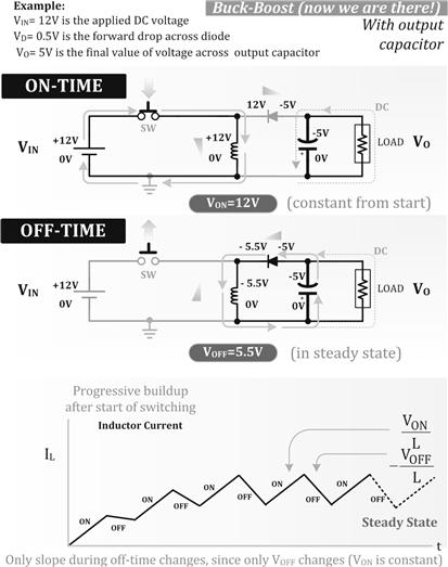
Figure 1.11: Evolution of the Buck-Boost topology.
In Figure 1.11, the current escalates initially, but then after several cycles, it automatically levels out in what is clearly a steady state. That is because every cycle the capacitor charges up, it progressively increases the slope of the down-ramp, eventually allowing the converter to settle down naturally into the basic condition ΔION=ΔIOFF ≡ ΔI. And once that is achieved, it is self-sustaining!
We also have a useful rail now — available across the output capacitor, from which we can draw some stored energy. So, we have shown a DC current passing through to the load by the dashed arrows in Figure 1.11.
In fact, this is our very first switching topology — the Buck-Boost topology.
Note: Under the abnormal condition of an output short for example, Figure 1.11 effectively reduces to Figure 1.10! Therefore, to protect the converter under such conditions, a current limit is required.
The Buck-Boost Converter
To understand Figure 1.11 better, we are actually going to work backward from here. So let us assume we have achieved a steady state — and therefore the output capacitor too has reached a steady value of say 5 V. Let us now find the conditions needed to make that a reality.
In Figure 1.11, the slope of the rising ramp is unchanged every cycle, being equal to VIN/L. The slope of the falling ramp is initially VD/L, where “VD” is the drop across the diode. So from the inductor equation, initially ΔION>ΔIOFF. Thus, the current starts to staircase. But the magnitude of the slope of the falling ramp, and therefore ΔIOFF, keeps getting larger and larger as the capacitor charges up. Eventually, we will reach a steady state defined by ΔIOFF=ΔION. At that moment, the voltseconds law applies.
![]()
Using the numbers of the example, we get
![]()
We see that a 5-V output is possible only if we have been switching with a constant ratio between the switch ON- and switch OFF-time, as given by
![]()
So to get the voltseconds to balance out for this case (5-V output and a 12-V input), we have to make the off-time 2.18 times larger than the on-time. Why so? Simply because the voltage during the on-time (across the inductor) is larger by exactly the same proportion: 12 V during the on-time as compared to 5.5 V during the off-time. Check: 12/5.5=2.18.
The duty cycle (assuming CCM) is therefore equal to
![]()
Now, had we taken a semiconductor switch instead of a mechanical one, we would have had a non-zero forward voltage drop of say “VSW.” This forward drop effectively just subtracts from the applied DC input during the on-time. So, had we done the above calculations symbolically, we would get
![]()
and
![]()
Then, from the voltseconds law
![]()
We thus get the duty cycle
![]()
If the switch and diode drops are small as compared to the input and output rails, we can simply write
![]()
We can also write the relationship between the input and the output as follows:
![]()
Note that some other easily derivable and convenient relationships to remember are
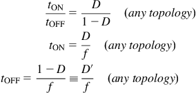
where we have defined D′ = 1 − D as the “duty cycle of the diode,” since the diode is conducting for the remainder of the switching cycle duration (in CCM).
Ground-Referencing Our Circuits
We need to clearly establish what is referred to as the “ground” rail in any DC–DC switching topology. We know that there are two rails by which we apply the DC input voltage (current goes in from one and returns from the other). Similarly, there are also two output rails. But all practical topologies generally have one rail that is common to both the input and the output. It is this common rail that, by convention, is called the system “ground” in DC–DC converter applications.
However, there is yet another convention in place — the ground is also considered to be “0 V” (zero volts).
The Buck-Boost Configurations
In Figure 1.12, the common (ground) rails have been highlighted in bold gray background.
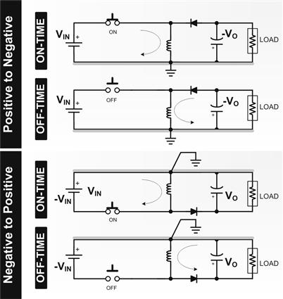
Figure 1.12: The two configurations of the Buck-Boost (inverting) topology.
We now realize that the Buck-Boost we presented in Figure 1.11 is actually a “positive (input)-to-negative (output)” Buck-Boost. There is another possibility, as shown in the lower half of Figure 1.12. We have relabeled its ground in accordance with the normal convention. Therefore, this is a “negative-to-positive Buck-Boost.”
For either configuration, we see that whatever polarity is present at the input, it gets reversed at the output. Therefore, the Buck-Boost is often simply called an “inverting” topology (though we should keep in mind that that allows for two different configurations).
The Switching Node
Very simply put — the “point of detour” for the inductor current, that is, between the switch and the diode, is called the “switching node.” Current coming into this node from the inductor can go either into the diode or into the switch, depending upon the state of the switch. Every DC–DC switching topology has this node (without it we would get the huge voltage spike we talked about!).
Since the current at this node needs to alternate between the diode and the switch, it needs to alternately force the diode to change state too (i.e., be reverse-biased when the switch turns ON and forward-biased when the switch is OFF). So, the voltage at this node must necessarily be “swinging.” An oscilloscope probe connected here (with its ground clip connected to the power supply ground, i.e., 0 V) will always see a voltage waveform with “square edges.” This is in fact very similar to the voltage across the inductor, except that it is DC level-shifted by a certain amount, depending on the topology.
On a practical level, while designing the PCB, we have to be cautious in not putting too much copper at the switching node. Otherwise it becomes an effective electric-field antenna, spewing radiated radio frequency interference all around. The output cables can thereafter pick up the radiated noise and transmit it directly to the load.
Analyzing the Buck-Boost
In Figure 1.13, we have drawn a line “IL” through the geometric center of the ramp portion of the steady-state inductor current waveform. This is defined as the average inductor current. The switch current also has an average value of IL, but only during the interval tON. Similarly, the average of the diode current is also IL during tOFF. However, the switch and diode currents when averaged over the entire cycle (i.e., over both the ON and OFF durations) are by simple mathematics their respective weighted averages.
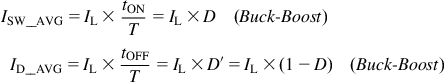
where D′ is the duty cycle of the diode, that is, 1−D. It is also easy to visualize that for this particular topology, the average input current is equal to the average switch current. Further, as we will see in the following sections, the average diode current is equal to the load current. This is what makes the Buck-Boost topology quite different from the Buck topology.
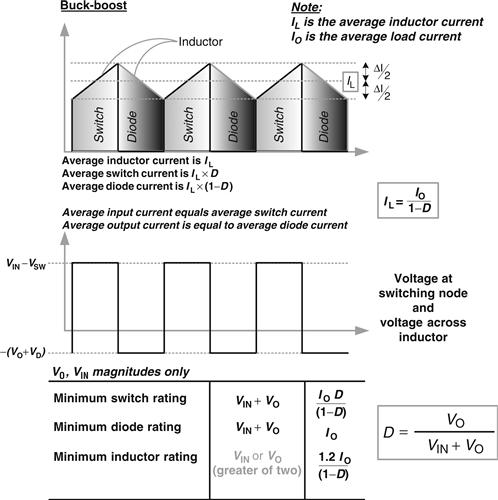
Figure 1.13: Analyzing the Buck-Boost.
Properties of the Buck-Boost
We now make some observations based on Figures 1.11–1.13:
• For example, a “positive-to-negative” Buck-Boost can convert 12 V to −5 V (step-down) or 12 V to −15 V (step-up). A “negative-to-positive” Buck-Boost can convert say −12 V to 5 V, or 5 V to 15 V, and so on. The magnitude of the output voltage can thus be either smaller or larger (or equal to) the magnitude of the input voltage.
• When the switch is ON, energy is delivered only into the inductor by the input DC source (via the switch), and none of it passes through to the output.
• When the switch is OFF, only the stored energy of the inductor is pushed into the output (through the diode), and none comes directly from the input DC source.
• The above two observations make the Buck-Boost topology the only “pure flyback” topology around, in the sense that all the energy transferred from the input to the output must have been previously stored in the inductor. No other topology shares this unique property.
• The current coming from the input capacitor (DC source) is “choppy,” that is, pulsating. That is because this current, combined with the steady DC current (IIN) coming in from the DC source, basically forms the switch current waveform (which we know is always choppy for any topology) (see Figure 1.9).
• Similarly, the current into the output capacitor is also choppy because combined with the steady DC current into the load (IOUT), it forms the diode current (which we know is always choppy for any topology) (see Figure 1.9).
• We know that heat dissipation is proportional to the square of the root mean square (RMS) current. And since choppy waveforms have high RMS values, the efficiency of a Buck-Boost is not very good. Also, there is generally a relatively high level of noise and ripple across the board. Therefore, the Buck-Boost may also demand much better filtering at its input, and often at its output too.
• Though current enters the output capacitor to charge it up when the switch turns ON and leaves it to go into the load when the switch is OFF, the average capacitor current is always zero. In fact, any capacitor in “steady state” must, by definition, have zero average current passing through it — otherwise it would keep charging or discharging until it too reaches a steady state, just like the inductor current.
Since the average current from the output capacitor is zero, therefore, for the Buck-Boost, the average diode current must be equal to the load current (where else can the current come from?). Therefore,
![]()
![]()
This is the relationship between the average inductor current and the load current. Note that in Figure 1.13, in the embedded table, we have asked for an inductor rated for 1.2×IO/(l−D). The factor “1.2” comes from the fact, that by typical design criteria, the peak of the inductor current waveform is about 20% higher than its average. So we need to look for an inductor rated at least for a current of 1.2×IL.
Why Three Basic Topologies Only?
There are certainly several ways to set up circuits using an inductor, which provide a “freewheeling path” too, for the inductor current. But some of these are usually disqualified simply because the input and output do not share a common rail, and thus there is no proper ground reference available for the converter and the rest of the system. Two examples of such “working-but-unacceptable” converters are the Buck-Boost configurations shown in Figure 1.14. Compare these with Figure 1.12 to see what the problem is! However, note that if these were “front-end converters,” the system ground could be established starting at the output of this converter itself and may thus be acceptable.
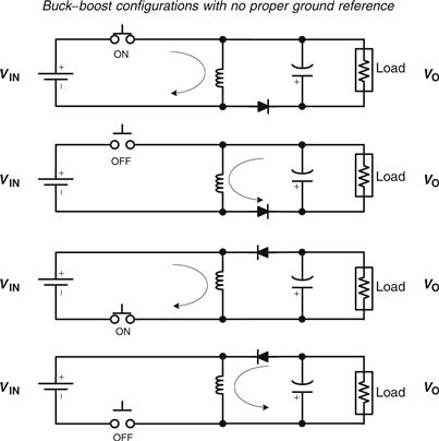
Figure 1.14: Improperly referenced Buck-Boost configurations.
Of the remaining ways, several are just “configurations” of a basic topology (like the two configurations in Figure 1.12). Among the basic topologies, we actually have just three — the Buck, the Boost, and the Buck-Boost. Why only three? That is because of the way the inductor is connected. Note that with proper ground-referencing in place, there are only three distinct rails possible — the input, the output, and the (common) ground. So if one end of the inductor is connected to the ground, it becomes a Buck-Boost! On the other hand, if it is connected to the input, it becomes a Boost. And if connected to the output, it becomes a Buck (see Figure 1.15).
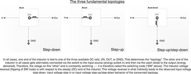
Figure 1.15: Three basic topologies possible only.
The Boost Topology
In Figure 1.16, we have presented the schematic of the Boost topology. The direct and the freewheeling paths are indicated therein. In Figure 1.17, we have the corresponding analysis, including the key waveforms.
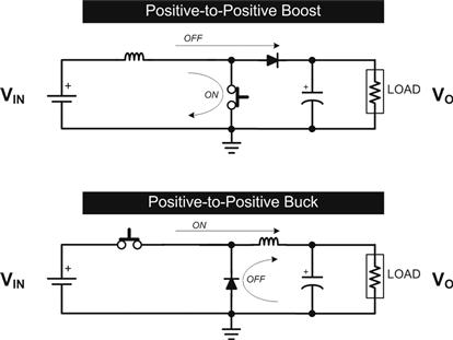
Figure 1.16: The (positive) Boost and Buck topologies.
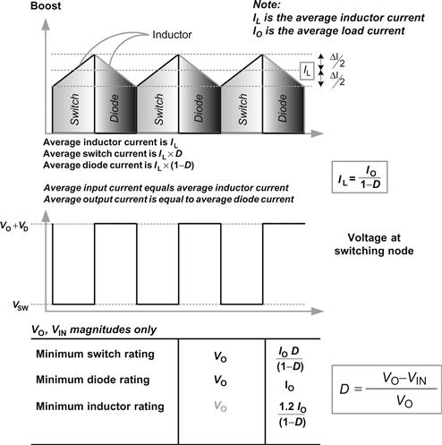
Figure 1.17: Analyzing the Boost.
We now make some observations:
• For example, a “positive-to-positive” Boost can convert 12 V to 50 V. A “negative-to-negative” Boost would be able to convert say −12 V to −50 V. The magnitude of the output voltage must therefore always be larger than the magnitude of the input voltage. So a Boost converter only steps-up and also does not change the polarity.
• In the Boost, when the switch is ON, energy is delivered only into the inductor by the input DC source (via the switch), and none of it passes through to the output.
• When the switch is OFF, the stored energy of the inductor is pushed into the output (through the diode). But some of it also comes from the input DC source.
• The current coming from the input capacitor (DC source) is “smooth,” since it is in series with the inductor (which prevents sudden jumps in current).
• However, the current into the output capacitor is “choppy” because combined with the steady DC current into the load (IOUT), it forms the diode current (which we know is always choppy for any topology) (see Figure 1.9).
• Since the average current from the output capacitor is zero, therefore, for the Boost, the average diode current must be equal to the load current (where else can the current come from?). Therefore,
![]()
![]()
This is the relationship between the average inductor current and the load current. Note that in Figure 1.17, in the embedded table, we have asked for an inductor rated for 1.2×IO/(l−D). The factor “1.2” comes from the fact that by typical design criteria, the peak of the inductor current waveform is about 20% higher than its average. So, we need to look for an inductor rated at least for a current of 1.2×IL.
Let us analyze the Boost topology in terms of the voltseconds in steady state. We have
![]()
and
![]()
So, from the voltseconds law
![]()
Performing some algebra on this to eliminate tOFF,
![]()
![]()
Finally, the “duty cycle” of the converter D, which is defined as
![]()
is the reciprocal of the preceding equation. So,
![]()
We have thus derived the classical DC transfer function of a Boost converter.
If the switch and diode drops are small as compared to the input and output rails, we can just write
![]()
We can also write the relationship between the input and output as follows:
![]()
The Buck Topology
In Figure 1.16, we had also presented the schematic of the Buck topology. The direct and the freewheeling paths are indicated therein. In Figure 1.18, we have the corresponding analysis, including the key waveforms.
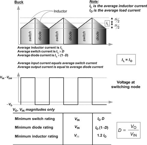
Figure 1.18: Analyzing the Buck.
We now make some observations:
• For example, a “positive-to-positive” Buck can convert 12 V to 5 V. A “negative-to-negative” Buck would be able to convert say −12 V to −5 V. The magnitude of the output voltage must therefore always be smaller than the magnitude of the input voltage. So, a Buck converter only steps-down and also does not change the polarity.
• When the switch is ON, energy is delivered to the inductor by the input DC source (via the switch). But some of it also passes through to the output.
• When the switch is OFF, the stored energy of the inductor is pushed into the output (through the diode). And none of it now comes from the input DC source.
• The current coming from the input capacitor (DC source) is “choppy.” That is because this current, combined with the steady DC current (IIN) coming in from the DC source, basically forms the switch current waveform (which we know is always choppy for any topology).
• However, the current into the output capacitor is “smooth” because it is in series with the inductor (which prevents sudden jumps in current).
• Since the average current from the output capacitor is zero, for the Buck, the average inductor current must be equal to the load current (where else can the current come from?). Therefore,
![]()
This is the relationship between the average inductor current and the load current. Note that in Figure 1.18, in the embedded table, we have asked for an inductor rated for 1.2×IO. The factor “1.2” comes from the fact that by typical design criteria, the peak of the inductor current waveform is about 20% higher than its average. So, we need to look for an inductor rated at least for a current of 1.2×IL.
Let us analyze the Buck topology in terms of the voltseconds in steady state. We have
![]()
and
![]()
As before, using the voltseconds law and simplifying, we get the “duty cycle” of the converter:
![]()
We have thus derived the classical DC transfer function of a Buck converter. If the switch and diode drops are small as compared to the input and output rails, we can just write
![]()
We can also write the relationship between the input and the output as follows:
![]()
Advanced Converter Design
This should serve as an introduction to understanding and designing switching power converters. More details and worked examples can be found in Chapter 2. The reader can also at this point briefly scan Chapter 4 for some finer nuances of design. A full design table is also available in the Appendix for future reference.