
Chapter 2
DC–DC Converter Design and Magnetics
This chapter deals with magnetics of DC–DC converters and explains the basic concepts behind peak, AC and DC values of the inductor current waveform. Duty cycle and DC transfer functions are explained. It also introduces the simplifying concept of current ripple ratio. The differences in behavior of the inductor current waveform with respect to input voltage variations and topology are highlighted. Optimum inductor design targets for each topology are thus provided. The worst-case input voltage is identified for correctly picking an inductor in wide-input DC–DC converters. Related topics such as current limit accuracy and also subharmonic instability when using current-mode control are introduced early on, since both these aspects can affect the final choice of inductor. Slope compensation is also introduced. The basics of magnetics theory including Faraday’s law are presented and a detailed worked example follows. All these factors help correctly size the inductor and settle on its most appropriate inductance. Conversions between CGS (centimeter-gram-seconds) and MKS (also called SI system) units are also provided along with estimation of core losses.
The reader is strongly advised to read Chapter 1 before attempting this chapter.
The magnetic components of any switching power supply are an integral part of its topology. The design and/or selection of the magnetics can affect the selection and cost of all the other associated power components, besides dictating the overall performance and size of the converter itself. Therefore, we really should not try to design a converter, without looking closely at its magnetics, and vice versa. With that in mind, in this chapter, we will be introducing the basic concepts of magnetics — in parallel with a formal DC–DC converter design procedure.
Note that in the area of DC–DC converters, we have only a single magnetic component to consider — its inductor. Further, in this particular area of power conversion, it is customary to just pick an off-the-shelf inductor for most applications. Of course there cannot possibly be enough “standard” inductors going around to cover all possible application scenarios. But the good news is that, given a certain inductor, and knowing its performance under a stated set of conditions, we can easily calculate how it will perform under our specific application conditions. And thereby, we can either validate or invalidate our initial selection. It may take more than one iteration or attempt, but moving in this direction, we can almost always find a standard inductor that fits our application.
In the next chapter we will introduce “off-line” power supply design. Such converters usually work off an AC (mains) input that ranges from 90 V to 270 V. To protect users from the high voltage, these converters almost invariably use an isolating transformer — in addition to, or in place of, the inductor. But though these topologies are really just derivatives of standard DC–DC topologies, in terms of magnetics, they are quite different. For example, we encounter significant (non-negligible) high-frequency effects within the transformer — like skin depth and proximity effects — the analysis of which can be quite challenging. In addition, we find that there are definitely not enough general-purpose (off-the-shelf) parts going around, that can meet all possible permutations and combinations of requirements, as can arise in off-line applications. So, in these applications, we usually always end up having to custom-design the magnetics. And as mentioned, this is not a mean task. But by trying to first understand DC–DC converter design, and the selection of off-the-shelf inductors, we are in a much better position to tackle off-line power supplies. We can thereby build up basic concepts and skills, while garnering a much-needed “feel” for magnetics.
Off-line converters and DC–DC converters are also relatively quite different in terms of some rather implicit (often completely unstated) differences in basic design strategy — like the issue relating to the size of the magnetics vis-à-vis the current limit of the converter, as we will soon learn. With regard to their similarities, we should remember that both can have a wide-input voltage range, not a single-value input voltage, as is often assumed in related literature. Having a wide input raises the following question — what voltage point within the prescribed input range is the “worst-case” (or maximum) for a given stress parameter? Note that in selecting a power component we often need to consider the worst-case stress it is going to endure in our application. And then, provided that the particular stress parameter happens to be a relevant and decisive factor in its selection, we usually add an additional amount of safety margin, for the sake of reliability. However, the problem is that different stress parameters do not attain their worst-case values at the same input voltage point. We, therefore, realize that the design of a wide-input converter is necessarily going to be “tricky.” For sure, designing a functional switching converter may be considered “easy,” but designing it well certainly isn’t.
Toward the end of this chapter, we will present a detailed DC–DC converter design procedure. But to account for a wide-input range, we will proceed in two distinct steps:
• A “general inductor design procedure,” for choosing and validating an off-the-shelf inductor for our application. We will see that depending on the topology at hand, this is to be carried out at a certain, specified voltage end — one that we will identify as being the “worst-case” from the viewpoint of the inductor.
• Then we will consider the other power components. We will point out which particular stress parameters are important in each case, and also the input voltage at which they reach their maximum, and how to ultimately select the component.
Note that, although the design procedure may be seen to specifically address only the Buck topology, the accompanying annotations clearly indicate how a particular step or equation may need to change if the procedure were being carried out for a Boost or a Buck-Boost topology.
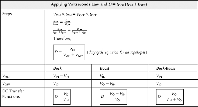
DC Transfer Functions
When the switch turns ON, the current ramps up in the inductor according to the inductor equation VON=L×ΔION/tON. The current increment during the on-time is ΔION=(VON×tON)/L. When the switch turns OFF, the inductor equation VOFF=L×ΔIΟΝ/tOFF leads to a current decrement ΔIOFF=(VOFF×tOFF)/L.
The current increment ΔION must be equal to the decrement ΔIOFF, so that the current at the end of the switching cycle returns to the exact value it had at the start of the cycle — otherwise we wouldn’t be in a repeatable (steady) state. Using this argument, we can derive the input–output (DC) transfer functions of the three topologies, as shown in Table 2.1. It is interesting to note that the reason why the transfer functions turn out different in each of the three cases can be traced back to the fact that the expressions for VON and VOFF are different. Other than that, the derivation and its underlying principles remain the same for all topologies.
Table 2.1. Derivation of DC Transfer Functions of the Three Topologies.
The DC Level and the “Swing” of the Inductor Current Waveform
From V=L dI/dt, we get ΔI=V Δt/L. So, the “swinging” component of the inductor current “ΔI” is completely determined by the applied voltseconds and the inductance. Voltseconds is the applied voltage multiplied by the time it is applied for. To calculate it, we can either use VON times tON (where tON=D/f), or VOFF times tOFF (where tOFF=(1−D)/f) — and we will get the same result (for that is how D gets defined in the first place!). But note also, that if we apply 10 V across a given inductor for 2 μs, we will get the same current swing ΔI, if we apply say, 20 V for 1 μs, or 5 V for 4 μs, and so on. So, for a given inductor, talking about either the voltseconds or the ΔI is effectively one and the same thing.
What does the voltseconds depend on? It depends on the input/output voltages (i.e. duty cycle) and time, via the switching frequency. Therefore, only by changing L, f, or D can we affect ΔI. Nothing else! See Table 2.2. In particular, changing the load current IO does nothing to ΔI. IO is therefore in effect, an altogether independent influence on the inductor current waveform. But what part of the inductor current does it specifically influence/determine? We will see that IO is proportional to the average inductor current.
Table 2.2. How Varying the Inductance, Frequency, Load Current, and Duty Cycle Influence ΔI and IDC.
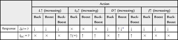
(↑↓) indicates it increases and decreases over the range; (×) indicates no change; (↑(=)) indicates IDC is increasing and is equal to IO.
a Maximum at D=0.5.
The inductor current waveform is considered to have another (independent) component besides its swing ΔI — it is the DC (average) level “IDC,” defined as the level around which the swing ΔI takes place symmetrically — that is, ΔI/2 above it, and ΔI/2 below it. See Figure 2.1. Geometrically speaking, this is the “center of the ramp.” It is sometimes also called the “platform” or “pedestal” of the inductor current. The important point to note is that IDC is based only on energy flow requirements — that is, the need to maintain an average rate of energy flow consistent with the input/output voltages and desired output power. So, if the “application conditions,” that is, the output power and the input/output voltages, do not change, there is in fact nothing we can do to alter this DC level — in that sense, IDC is rather “stubborn” (see Figure 2.1). In particular
• Changing the inductance L doesn’t affect IDC.
• Changing the frequency f doesn’t affect IDC.
• Changing the duty cycle D does affect IDC — for the Boost and Buck-Boost.
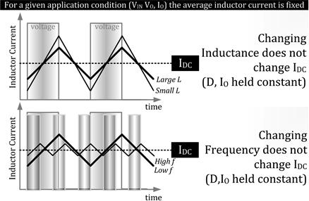
Figure 2.1: If D and IO are fixed, IDC cannot change.
To understand the last bullet above, we should note the following equations that we will derive a little later
![]()
![]()
The intuitive reason why the above relations are different is that in a Buck, the output is in series with the inductor (from the standpoint of the DC currents, the output capacitor contributes nothing to the DC current distribution), and therefore the average inductor current must at all times be equal to the load current. Whereas, in a Boost and Buck-Boost, the output is in series with the diode, and so the average diode current must equal the load current.
Therefore, if we keep the load current constant, and change only the input/output voltages (duty cycle), we can affect IDC — in all cases except for the Buck. In fact, the only way to change the DC inductor current level for a Buck is to change the load current. Nothing else will work!
In the Buck, IDC and IO are equal. But in the Boost and Buck-Boost, IDC depends also on the duty cycle. That makes the design/selection of magnetics for these two topologies rather different from a Buck. For example, if the duty cycle is 0.5, the average inductor current is twice the load current. Therefore, using a 5 A inductor for a 5 A load current may be a recipe for disaster. But for a Buck it is OK except for high-voltage applications (discussed later).
One thing we can be sure of is that in the Boost and Buck-Boost, IDC is always greater than the load current. We may be able to cause this DC level to fall and even approach the load current value if we reduce the duty cycle close to 0 (i.e., a very small difference between the input and output voltages). But then, on increasing the duty cycle toward 1, the DC level of the inductor current will climb steeply. It is important we recognize this clearly and early on.
Another thing we can conclude with certainty is that in all the topologies, the DC level of the inductor current is proportional to the load current. So, doubling the load current for example (keeping everything else the same), doubles the DC level of the inductor current (whatever it was to start with). So, in a Boost with a duty cycle of 0.5 for example, if we have a 5 A load, then the IDC is 10 A. And if IO is increased to 10 A, IDC will become 20 A.
Changing the input/output voltages (i.e. duty cycle) does affect the DC level of the inductor current for the Boost and the Buck-Boost. Changing D also affects the swing ΔΙ in all three topologies, because it changes the duration of the applied voltage and thereby changes the voltseconds. Summarizing:
Note: The off-line Forward converter transformer is probably the only known exception to the above logic. We will learn that if we, for example, double the duty cycle (i.e., double tON), then almost coincidentally, VON halves, and therefore the voltseconds does not change (and nor does ΔI). In effect, ΔI is then independent of duty cycle.
Based on the discussions above, and also the detailed design equations, we have summarized these “variations” in Table 2.2. This table should hopefully help the reader eventually develop a more intuitive and analytical “feel” for converter and magnetics design, one which can come in handy at a later stage. We will continue to discuss certain aspects of this table, in more detail, a little later.
Defining the AC, DC, and Peak Currents
In Figure 2.2, we see how the AC, DC, peak-to-peak, and peak values of the inductor current waveform are defined. In particular, we note that the AC value of the current waveform is defined as
![]()
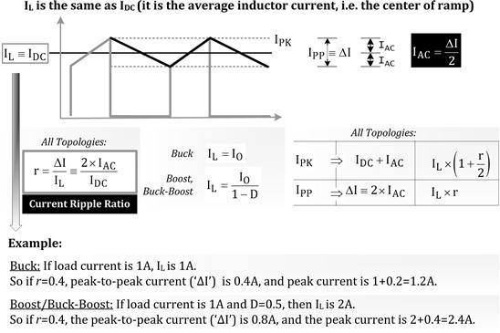
Figure 2.2: The AC, DC, peak, and peak-to-peak currents, and the current ripple ratio “r” defined.
We should also note from Figure 2.2 that IL ≡ IDC. Therefore, sometimes in our discussions that follow, we may refer to the DC level of the inductor current as “IDC ” and sometimes as the average inductor current “ΙL ” but they are actually synonymous. In particular, we should not get confused by the subscript “L” in “IL.” The “L” stands for inductor, not load. The load current is always designated as “IO.” Of course, we do realize that IL=IO for a Buck, but that is just happenstance.
In Figure 2.2 we have also defined another key parameter called “r,” or the “current ripple ratio.” This connects the two independent current components IDC and ΔI. We will explore this particular parameter in much greater detail a little later. Here, it suffices to mention that r needs to be set to an “optimum” value in any converter — usually approximately 0.3–0.5, irrespective of the specific application conditions, the switching frequency, and even the topology itself. This, therefore, becomes a universal design rule of thumb. We will also learn that the choice of r affects the current stresses and dissipation in all the power components, and thereby impacts their selection. Therefore, setting r should be the first step when commencing any power converter design.
The DC level of the inductor current (largely) determines the I2R losses in the copper windings (‘copper loss’). However, the final temperature of the inductor is also affected by another term — the “core loss” — that occurs inside the magnetic material (core) of the inductor. Core loss is, to a first approximation, determined only by the AC (swinging) component of the inductor current (ΔI), and is therefore virtually independent of the DC level (IDC or “DC bias”).
We must pay the closest attention to the peak current. Note that in any converter, the terms “peak inductor current,” “peak switch current,” and “peak diode” current are all synonymous. Therefore, in general, we just refer to all of them as simply the “peak current” IPK where
![]()
The peak current is in fact the most critical current component of all — because it is not just a source of long-term heat buildup and consequent temperature rise, but a potential cause of immediate destruction of the switch. We will show later that the inductor current is instantaneously proportional to the magnetic field inside the core. So, at the exact moment when the current reaches its peak value, so does this field. We also know that real-world inductors can “saturate” (start losing their inductance) if the field inside them exceeds a certain “safe” level — that value being dependent on the actual material used for the core (not on the geometry, or number of turns or even the air-gap, for example). Once saturation occurs, we may get an almost uncontrolled surge of current passing through the switch — because, the ability to limit current (which is one of the reasons the inductor is used in switching power supplies in the first place), depends on the inductor behaving like one. Therefore, losing inductance is certainly not going to help! In fact, we usually cannot afford to allow the inductor to “saturate” even momentarily. And for this reason, we need to monitor the peak current closely (usually on a cycle-by-cycle basis). As indicated, the peak is the likeliest point of the inductor current waveform where saturation can start to occur.
Note: A slight amount of core saturation may turn out to be acceptable on occasion, especially if it occurs only under temporary conditions, like power-up for example. This will be discussed in more detail later.
Understanding the AC, DC, and Peak Currents
We have seen that the AC component (IAC=ΔI/2) is derivable from the voltseconds law. From the basic inductor equation V=L dI/dt, we get
![]()
So, the current swing IPP ≡ ΔI, can be intuitively visualized as “voltseconds per unit inductance.” If the applied voltseconds doubles, so does the current swing (and AC component). And if the inductance doubles, the swing (and AC component) is halved.
Let us now consider the DC level again. Note that any capacitor has zero average (DC) current through it in steady state, so all capacitors can be considered to be “missing altogether” when calculating DC current distributions. Therefore, for a Buck, since energy flows into the output during both the on-time and off-time, and via the inductor, the average inductor current must always be equal to the load current. So,
![]()
On the other hand, in both the Boost and the Buck-Boost, energy flows into the output only during the off-time, and via the diode. Therefore, in this case, the average diode current must be equal to the load current. Note that the diode current has an average value equal to IL when it is conducting (see the dashed line passing through the center of the down-ramp in the upper half of Figure 2.3). But if we calculate the average of this diode current over the entire switching cycle, we need to weight it by its duty cycle, that is, 1−D. Therefore, calling “ID” the average diode current, we get
![]()
solving
![]()
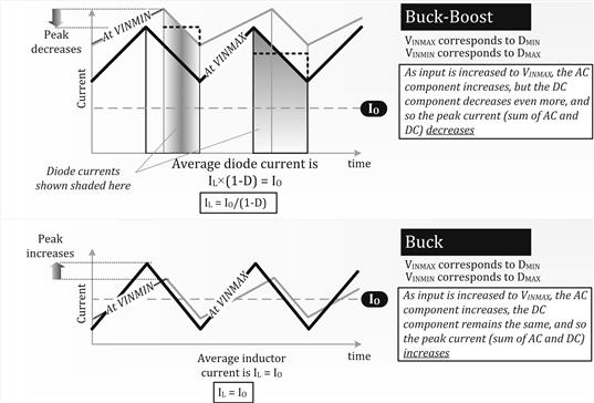
Figure 2.3: Visualizing the AC and DC components of the inductor current as input voltage varies.
Note also, that for any topology, a high-duty cycle corresponds to a low-input voltage, and a low-duty cycle is equivalent to a high input. So, increasing D amounts to decreasing the input voltage (its magnitude) in all cases. Therefore, in a Boost or Buck-Boost, if the difference between the input and output voltages is large, we get the highest DC inductor current.
Finally, with the DC and AC components known, we can calculate the peak current using
![]()
Defining the “Worst-Case” Input Voltage
So far, we have been implicitly assuming a fixed input voltage. In reality, in most practical applications, the input voltage is a certain range, say from “VINMIN” to “VINMAX.” We therefore also need to know how the AC, DC, and peak current components change as we vary the input voltage. Most importantly, we need to know at what specific voltage within this range we get the maximum peak current. As mentioned, the peak is critical from the standpoint of ensuring there is no inductor saturation. Therefore, defining the “worst-case” voltage (for inductor design) as the point of the input voltage range where the peak current is at its maximum, we need to design/select our inductor at this particular point always. This is in fact the underlying basis of the “general inductor design procedure” that we will be presenting soon.
We will now try to understand where and why we get the highest peak currents for each topology. In Figure 2.3, we have drawn various inductor current waveforms to help us better visualize what really happens as the input is varied. We have chosen two topologies here, the Buck and the Buck-Boost, for which we display two waveforms each, corresponding to two different input voltages. Finally, in Figure 2.4 we have plotted out the AC, DC, and peak values. Note that these plots are based on the actual design equations, which are also presented within the same figure. While interpreting the plots, we should again keep in mind that for all topologies, a high D corresponds to a low input. The following analysis will also explain certain cells of the previously provided Table 2.2, where the variations of ΔI and IDC, with respect to D, were summarized.
a) For the Buck, the situation can be analyzed as follows:
• As the input increases, the duty cycle decreases in an effort to maintain regulation. But the slope of the down-ramp ΔI/tOFF cannot change, because it is equal to VOFF/L, that is, VO/L, and we are assuming VO is fixed. But now, since tOFF has increased, but the slope ΔI/tOFF has not changed, the only possibility is that ΔI must have increased (proportionally). So, we conclude that the AC component of the Buck inductor current actually increases as the input increases (even though the duty cycle decreased in the process).
• On the other hand, the center of the ramp IL is fixed at Io, so we know the DC level does not change.
• Finally, since the peak current is the sum of the AC and DC components, it increases at high-input voltages (see relevant plot in Figure 2.4).
Therefore, for a Buck, it is always preferable to start the inductor design at VINMAX (i.e., at DMIN).
b) For the Buck-Boost, the situation can be analyzed as follows:
• As the input increases, the duty cycle decreases. But the slope of the down-ramp ΔI/tOFF cannot change, because it is equal to VOFF/L, that is, VO/L, and VO is fixed (same situation as for the Buck). But since tOFF has increased, ΔI must also increase to keep the slope ΔI/tOFF unchanged. So, we see that the AC component (ΔI/2) increases as the input increases (duty cycle decreasing). Note that up till this point, the analysis is the same as for the Buck — traced back to the fact that in both these topologies VOFF=VO.
• But now coming to the DC level IL of the Buck-Boost, we will find it must change for this topology (it remained fixed for the Buck). Note that the shaded portion of the waveform in the upper half of Figure 2.3 represents the diode current. The average value of this during the off-time is the square dashed line passing through its center, that is, IL. So, the average diode current, calculated over the entire switching cycle, is IL×(1−D). And we know this must equal the load current IO. Therefore, as the input increases and duty cycle decreases, the term (1−D) increases. So, the only way IL×(1−D) can remain constant at the value IO is if IL decreases as D decreases. We therefore realize that the DC level decreases as the input increases (duty cycle decreasing).
• Since the peak current is the sum of the AC and DC components, it also decreases at high-input voltages (see relevant plot in Figure 2.4).
Therefore, for a Buck-Boost, we should always start the inductor design at VINMIN (i.e., at DMAX).
c) For the Boost, the situation is a little trickier to understand. On the face of it, it is quite similar to the Buck-Boost, but there is a notable difference — and that is why we did not even try to include it in Figure 2.3.
• Once again, as the input increases, the duty cycle decreases. But the difference here is that the slope of the down-ramp ΔI/tOFF must decrease — because it is equal to VOFF/L, that is, (VO−VIN)/L (magnitudes only) — and we know that VO−VIN is decreasing. Further, the required decrease in the slope ΔI/tOFF can come about in two ways — either from an increase in tOFF (which is already occurring as the duty cycle decreases), or from a decrease in ΔI. In fact, ΔI is allowed to increase or decrease (as we increase the input). For example, if tOFF increases faster than ΔI — then ΔI/tOFF will still decrease as required. And in practice, that is what actually does happen in the case of the Boost. With some detailed math, we can show that ΔI increases as D approaches 0.5, but decreases after that (see Table 2.2 and Figure 2.4).
• However, the increase/decrease in the AC level does not dominate in a Boost, and therefore, the peak current ends up being dictated only by the DC component. But we already know that the DC level of a Boost changes in exactly the same way as for the Buck-Boost (discussed above) — it decreases as the input increases (duty cycle decreasing).
• We conclude that the peak current for the Boost decreases at high-input voltages (see relevant plot in Figure 2.4).
Therefore, for a Boost, we should always start the inductor design at VINMIN (i.e., at DMAX).
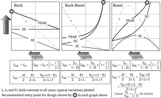
Figure 2.4: Plotting how the AC, DC, and peak currents change with duty cycle.
The Current Ripple Ratio “r”
In Figure 2.2, we first introduced the most basic, yet far-reaching design parameter of the power supply itself — its current ripple ratio “r.” This is a geometrical ratio that compares and connects the AC value of the inductor current to its associated DC value. So,
![]()
Here, we have used ΔI=2×IAC. Once r is set by the designer (at maximum load current and worst-case input), almost everything else is pre-ordained — like the currents in the input and output capacitors, the “RMS” (root mean square) current in the switch, and so on. Therefore, the choice of r affects component selection and cost, and it must be understood clearly, and picked carefully.
Note that the ratio r is defined for CCM (continuous conduction mode) operation only. Its valid range is from 0 to 2. When r is 0, ΔI must be 0, and the inductor equation then implies a very large (infinite) inductance. Clearly, r=0 is not a practical value! If r equals 2, the converter is operating at the boundary of continuous and discontinuous conduction modes (boundary conduction mode or “BCM”) (see Figure 1.9 and Figure 2.5). In this so-called boundary (or “critical”) conduction mode, IAC=IDC by definition. Note that readers can refer back to Chapter 1, in which CCM, DCM (discontinuous conduction mode), and BCM were all initially introduced and explained.
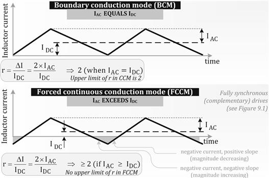
Figure 2.5: BCM and forced CCM operating modes.
Note that an exception to the “valid” range of r from 0 to 2 occurs in “forced CCM” mode, discussed in more detail later.
Relating r to the Inductance
We know that current swing is given as voltseconds per unit inductance. So, we can also write
![]()
Here “Et” is defined as the (magnitude of the) voltmicroseconds across the inductor (either during the on-time or off-time — both being necessarily equal in steady state), and LμH is the inductance in μΗ. The reason for defining Et is that this number is simply easier to manipulate than voltseconds because of the very small time intervals involved in modern power conversion.
Therefore, the current ripple ratio is
![]()
Note also that from now on, whenever L is paired up with Et in any given equation, we will drop the subscript of L, that is, “μΗ.” It will then be “understood” that L is in μΗ.
Finally, we have the following key relationships between r and L:
![]()
Incidentally, the preceding equation, that is, the one involving VOFF, assumes CCM, because it assumes that tOFF (the time for which VOFF is applied) is equal to the full available off-time (1−D)/f.
Conversely, L as a function of r is
![]()
In subsequent sections we will often use the following easy-to-remember form of the previous equations. We are going to nickname this the “L×I” equation (or rule)
![]()
But perhaps we are still wondering — why do we even need to talk in terms of r — why not talk directly in terms of L? We do realize from the above equations that L and r are related. However, the “desirable” value of inductance depends on the specific application conditions, the switching frequency, and even the topology. So, it is just not possible to give a general design rule for picking L. But there is in fact such a general design rule of thumb for selecting r — one that applies almost universally. We mentioned that it should be approximately 0.3–0.5 in all cases. And that is why it makes sense to calculate L by first setting the value of r. Of course, once we pick r, L gets automatically determined for a given set of application conditions and switching frequency.
The Optimum Value of r
It can be shown that, in terms of overall stresses in a converter and size, r ≈ 0.4 represents an “optimum” of sorts. We will now try to understand why this is so, and later we will try to point out exceptions to this reasoning.
The size of an inductor can be thought of as being virtually proportional to its energy-handling capability (the effect of air-gap on size will be studied later). So, for example, we probably already know intuitively that we need bigger cores to handle higher powers. The energy-handling capability of the selected core must, at a bare minimum, match the energy we need to store in it in our application — that is, ![]() . Otherwise, the inductor will saturate. (Later, read Chapter 5 to understand the related topology-dependency aspect.)
. Otherwise, the inductor will saturate. (Later, read Chapter 5 to understand the related topology-dependency aspect.)
In Figure 2.6, we have plotted the energy, ![]() , as a function of r. We see that it has a “knee” at around 0.4. This tells us that if we try to reduce r much lower than 0.4, we will certainly need a very large inductor. On the other hand, if we increase r, there isn’t much greater reduction in the size of the inductor. In fact, we will see that beyond r ~ 0.4, we enter a region of diminishing returns.
, as a function of r. We see that it has a “knee” at around 0.4. This tells us that if we try to reduce r much lower than 0.4, we will certainly need a very large inductor. On the other hand, if we increase r, there isn’t much greater reduction in the size of the inductor. In fact, we will see that beyond r ~ 0.4, we enter a region of diminishing returns.
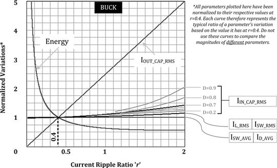
Figure 2.6: How varying the current ripple ratio r affects all the components.
In Figure 2.6, we have also plotted the capacitor RMS currents for a Buck converter. We see that if r is increased beyond 0.4, the currents will increase significantly. This will lead to increased heat generation inside the capacitors (and other related components too). Eventually, we may be forced to pick a capacitor with a lower ESR and/or lower case-to-air thermal resistance (more expensive/bigger).
Note: The RMS value of the current through any component is the current component responsible for the heat developed in it — via the equation P=IRMS2×R, where P is the dissipation, and R is the series resistance term associated with the particular component (e.g., the DC resistance (DCR) of an inductor, or the ESR of a capacitor). However, it can be shown that the switch, diode, and inductor RMS current values are not very “shape-dependent.” Therefore, the heat developed in them does not depend much on r , but mainly on the average value of the current. On the other hand, the RMS of the capacitor current waveforms can increase significantly, if r is increased. So, capacitor currents are very “shape-dependent,” and therefore depend strongly on r. The reason for that is fairly obvious — any capacitor in a steady state has zero average (DC) current through it. Since a capacitor effectively subtracts out the DC level of the accompanying current waveform, we are left with a capacitor current waveform that has a large “ramp portion” built-in into it. Therefore, changing r changes this ramp portion, thereby impacting the capacitor current greatly.
Note that in Figure 2.6, though we have used the Buck topology as an example, the energy curve in particular is exactly the same for any topology. The capacitor current curves though, may not be identical to those of the Buck, but are similar, and so the conclusions above still apply.
Therefore, in general, a current ripple ratio of around 0.4 is a good design target for any topology, any application, and any switching frequency.
Later, we will discuss some reasons/considerations for not adhering to this r~0.4 rule of thumb (under certain conditions).
Do We Mean Inductor? or Inductance?
Note that in the previous section, we said nothing explicitly about what the inductance was — we just talked about the size of the inductor. We know that in theory, we can put almost any number of turns on a given core, and get almost any inductance. So, inductance and size of inductor are not necessarily related. However, we will now see that in power conversion they often do turn out to be so, though rather indirectly.
Looking at Figure 2.6, we can see that a smaller r will require a higher energy-handling capability, and thus a larger inductor. Let us now formally go through all the possible ways of reducing r.
Since we are assuming our application conditions are fixed, the load current and input/output voltages are also fixed. Therefore, IDC is fixed too. The only way we can cause r to decrease under these circumstances is to make ΔI smaller. However, ΔI is
![]()
But we know the applied voltseconds is fixed too (input and output voltages being fixed). So, the only way to decrease r (for a given set of application conditions) is to increase the inductance. We can therefore conclude that if we choose a high inductance, we will invariably require a bigger inductor. It is therefore no surprise that when power supply designers instinctively ask for a “large inductance,” they might well mean a “large inductor.” Therefore, the designer is cautioned against being too “ripple-phobic” in their designs. A certain amount of ripple is certainly “healthy.”
However, we must not forget that if, for example, we increase the load current (i.e., a change in application conditions), and we will clearly need to move to a larger inductor (with greater energy-handling capability). But simultaneously, we will need to decrease the inductance. That’s because IDC will increase, and so to keep to the “optimum” value of r, we will need to increase ΔI in the same proportion as the increase in IDC. And to do this, we have to decrease, rather than increase, L.
This highlights the importance of thinking in terms of r to ease power supply design.
How Inductance and Inductor Size Depend on Frequency
The following discussion applies to all the topologies.
If keeping everything else fixed (including D) we double the frequency, the voltseconds will halve, because the durations tON and tOFF have halved. But since ΔI is “voltseconds per unit inductance,” it too will halve. Further, since IDC has not changed, r=ΔI/IDC will also halve. So, if we started off with r=0.4, we now have r=0.2.
If we want to return the converter to the optimum value of r=0.4, we will now need to somehow double the ΔI (that we were left with at the end of the last step). The way to do that is to halve the inductance.
• Therefore, we can generally state that inductance is inversely proportional to frequency. Finally, having restored r to 0.4, the peak will still be 20% higher than the DC level. But the DC level has not changed. So, the peak value is also unchanged (since r hasn’t changed either, eventually). However, the energy-handling requirement (size of inductor) is ![]() . Now, since L has halved, and IPK is unchanged, the required size of the inductor has halved.
. Now, since L has halved, and IPK is unchanged, the required size of the inductor has halved.
• Therefore, we can generally state that the size of the inductor is inversely proportional to frequency.
• Note also that the required current rating of the inductor is independent of the frequency (since peak is unchanged).
How Inductance and Inductor Size Depend on Load Current
For all topologies, if we double the load current (keeping input/output voltages and D fixed), r will tend to halve since ΔI has not changed but IDC has doubled. Therefore, to restore r to its optimum value of 0.4, we need to get ΔI to double too. But we know that ΔI is simply “voltseconds per unit inductance,” and in this case the voltseconds has not changed. So, the only way to get ΔI to double is to halve the inductance.
• Therefore, we can generally state that inductance is inversely proportional to the load current.
What about the size? Since we doubled the load current, but still kept r at 0.4, the peak current IDC(1+r/2) has also doubled. But the inductance has halved. So, the energy-handling requirement (size of inductor), ![]() , will double.
, will double.
• Therefore, we can generally state that the size of the inductor is proportional to the load current.
How Vendors Specify the Current Rating of an Off-the-shelf Inductor and How to Select It
The “energy-handling capability” of an inductor, 1/2×LI2, is one way of picking the size of the inductor. But most vendors do not provide this number upfront. However, they do provide one or more “current ratings” for us to decipher. And if we interpret these current rating(s) correctly, that serves the purpose.
The current rating may be expressed by the vendor either as a maximum rated IDC, or a maximum rated IRMS, or/and a maximum ISAT. The first two are usually considered synonymous, since the RMS and DC values of a typical inductor current waveform are almost equal (we had indicated previously that the RMS of the inductor current is not very “shape-dependent”). So, the DC/RMS rating of an inductor is by definition basically the direct current we can pass through it, such that we get a specified temperature rise (typically 40–55°C depending on the vendor). The last rating, that is, the ISAT, is the maximum current we can pass, just before the core starts saturating. At that point, the inductor is considered close to the useful limit of its energy-storing capability.
We will also find that many, if not most, vendors have chosen the wire gauge in such a manner that the IDC and ISAT ratings of any inductor are also virtually the same. And by doing this, they can publish one (single) current rating — for example, “the inductor is rated for 5 A.” Basically, having determined the ISAT of the inductor, the vendor has then consciously tweaked the wire gauge (at the saturation current level), so as to also get the specified temperature rise.
The rationale for wanting to set IDC=ISAT is as follows — suppose the inductor had a DC rating of 3 A and an ISAT of 5 A. The 5-A rating is then likely to be superfluous, because users would probably never select this inductor for an application that required more than 3 A anyway. Therefore, the excessive ISAT rating in this case essentially amounts to an unnecessarily over-sized core. Of course, if we do find an inductor with different IDC and ISAT ratings, it is also possible the vendor may have (unsuccessfully) tried to exploit the larger size of the chosen core (by increasing the wire thickness), but the stumbling block was that the selected core geometry was somehow not conducive to doing so — maybe it just did not have enough window space for accommodating the thicker windings.
In general, an inductor with a “single” current rating is usually the most optimum/cost-effective too.
However, in some rare off-the-shelf inductors, we may even find ISAT stated to be less than IDC. But what use is that? We can’t operate beyond ISAT in any case! So, the only advantage, if any, that can be gleaned from such an inductor is that the temperature rise in a real application will be less than the maximum specified. Automotive applications?
In general, for most practical purposes, the current rating of the inductor that we need to consider is the lowest rating of all the published current ratings. We can usually simply ignore all the rest.
There are some subtle considerations and exceptions to the argument for always preferring an inductor with IDC ≈ ISAT. For example, under transient/temporary conditions, the momentary current may exceed the normal steady operating current by a wide margin. So, for example, suppose we are using a switcher with an internally fixed current limit “ICLIM” or “ILIM” of 5 A — in a 3-A application. Then under startup (or sudden line/load steps), the current is very likely to hit the limiting value of 5 A for several cycles in succession as the control circuitry struggles to bring up the output rail into regulation. We will discuss this issue in greater detail below — in particular, whether this is even a concern to start with! However, assuming for now that it is, it then seems that it may actually make sense to use an inductor rated for 3 A continuous current, with an ISAT rating of 5 A (provided such an inductor is freely available, and cheap). Of course, alternatively, we could just pick a standard “5 A inductor” (for the 3-A application), and thereby we would certainly avoid inductor saturation under all conditions (and the consequent likelihood of switch destruction). But we realize that in doing so, our inductor may be considered slightly over-designed from the viewpoint of its copper/temperature rise — the wire being unnecessarily thicker. However, we should keep in mind that larger cores certainly affect cost, but a little more copper rarely does!
What Is the Inductor Current Rating We Need to Consider for a Given Application?
Whenever we start-up, or subject the converter to sudden line/load transients, the current no longer stays at the steady value it has under normal operation (i.e., when delivering the required maximum rated load current). For example, if we suddenly short the output the control circuitry in an effort to regulate the output may momentarily expand the duty cycle to the highest permissible value (as set by the controller). We then are no longer in steady state, and so under the increased on-time voltseconds, the current ramps up progressively, and can reach the set current limit.
But then, the inductor would probably be saturating! For example, if we are using a 5-A fixed current limit Buck switcher IC for a 3-A application, we have probably picked an inductor rated for only around 3 A. But when we short the output, the current momentarily hits the current limit (which may be set typically around 5.3 A for a “5-A Buck switcher”).
So the question is — should we select an inductor with a rating based on the current limit threshold (that it may encounter under severe transients), or simply on the basis of the maximum continuous normal operating current (under steady state operation in our application)? In fact, this question is not as philosophical as it may seem — it virtually separates standard industry off-line design procedures from those of DC–DC converters. To answer it effectively, a lot of factors may need to be considered, often on an individual or case-by-case basis. Let us address some of these concerns next.
Luckily, in most low-voltage applications, a certain amount of core saturation doesn’t cause any problem. The reason for this is that if in the above example, the switch is rated for 5 A, and the current-limiting circuit in the IC is known to act fast enough to prevent the current from ever rising beyond 5 A, then even if the inductor has started saturating as it gets to 5 A, there is no cause for concern — after all, if the switch doesn’t break, we don’t have a problem! And since the current doesn’t exceed 5 A, the switch cannot break. Hence, in this case, we could certainly pick a cost-effective “3-A inductor” for our application, knowing well in advance that it would saturate somewhat under various non-steady conditions. Of course we don’t want to operate a switching converter constantly (under its rated maximum load conditions) with a saturating inductor — we just “allow” it to do so under abnormal and temporary conditions, so long as we are sure that the switch can never be damaged.
However, the above logic begs another key question to be answered — what exactly constitutes “fast enough” — that is, which factors affect our ability to turn the switch OFF fast enough to protect it from the consequences of a saturating inductor? Since this consideration may eventually end up dictating the size and cost of the inductor, it is important to understand this response-time issue well.
(a) All current limit circuitry takes some finite time to respond. There are inherent (internal) “propagation delays” as we move the overcurrent signal through the internal comparators of the IC, its op-amps, level-shifters, driver, and so on to the IC pin driving the switch.
(b) If we are using a controller IC (as opposed to an “integrated switcher,” i.e., with an internal switch), the switch will necessarily be at a certain physical distance from its driver (which is usually inside the IC). In that case, the parasitic inductances of the intervening PCB traces (roughly 20 nH/in. of trace) will resist any sudden change in current, thereby creating an additional delay before the turn-off command issued by the IC actually reaches the Gate/Base of the switch.
(c) Theoretically speaking, even if the current-limiting circuitry had responded immediately to the overcurrent condition, and if the intervening traces had truly negligible inductance, the switch may still take a little time before it really turns itself OFF. During this delay, if the inductor is saturating, it will not be able to effectively prevent or limit the current spike that can get pushed through the transistor by the applied input DC source. The current could go well beyond the “safe” current limit threshold.
Bipolar junction transistors (BJTs) are inherently slow, as compared to more modern devices like MOSFETs. But large MOSFETs (e.g., high-current, high-voltage devices) also produce delays because of their higher internal parasitic Gate resistance and inductance and significant inter-electrode parasitic capacitances (that demand to be either discharged or charged as the case may be, before they allow the switch to change its state). Matters can get worse if we parallel several such MOSFETs together, as say for a very high-current application.
(d) Many controllers and ICs incorporate an internal “blanking time” — during which they deliberately “do not look” at the current waveform. The basic purpose is to avoid false triggering of the current limit circuitry by the noise generated at the turn-on transition. But this delay time could prove fatal to the switch, especially if the inductor has already started saturating, because the current limit circuitry won’t even “know” if there is any overcurrent condition during this blanking interval. Further, in current-mode control ICs, the ramp to the PWM (pulse-width modulator) comparator stage is usually derived from the (noisy) switch current. So, the blanking time is typically set even higher — typically about 100 ns for low-voltage applications and up to 300 ns for off-line applications.
(e) Integrated high-frequency switchers (i.e., with the MOSFET or BJT switch contained within the same package as the control and driver) are usually the best-protected and most reliable, because the intervening inductances are minimized. Also, the blanking times can be set more accurately and optimally, since there is not going to be much variation in terms of different switches with widely varying characteristics. Therefore, integrated switchers can usually survive momentarily saturating inductors with almost no problem — unless the input voltage is very high (typically above 40–60 V), and in addition, the inductor is sized “very small.”
(f) If the input voltage is high, the rate of rise of the saturating inductor current ramp can become very large (“steep”). This follows from the basic equation V=L dI/dt. Here, if L→0, since V is fixed, the dI/dt must increase dramatically (see Figure 2.7). So now, even a small delay can prove fatal because a large ΔI can take place during a very small interval. The current can therefore overshoot the set current limit threshold by a very large amount, thereby endangering the switch. That is why, especially when we come to off-line applications, it is actually customary to select a core large enough to avoid saturation at the current limit threshold. And that usually gives enough time for the current limit circuitry to act — before the slope of the current has gone completely out of control.
Note however, that the copper windings still only need to be proportioned to handle the continuous current (i.e., based on the maximum operating load).
In effect, what we are always implicitly doing in off-line applications is designing the transformer such that its ISAT is higher than its IDC rating. That is clearly not what we usually do in low-voltage DC–DC converter design, where we tend to equate the two.
(g) Generally speaking, in most low-voltage applications (i.e., VIN typically less than about 40 V), the inductors are selected based only on the maximum operating load current. The set current limit is therefore, in effect, virtually ignored! This is the usual industry practice for DC–DC converter design, though it is probably not clearly spelled out in this way most of the time. Luckily, it seems to have worked!
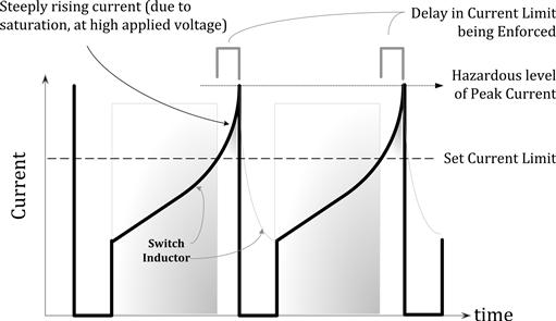
Figure 2.7: How higher voltages combined with inherent response-time delays can cause overstress in the switch when the inductor starts saturating.
The Spread and Tolerance of the Current Limit
Any specification, including the current limit, either set by the user or fixed internally in the IC, will have a certain inherent tolerance band — that includes spreads over process variations and over temperature. All these variations are combined together inside the electrical tables of the datasheet of the device, under its “MIN” and “MAX” limits. In a practical converter design, a good designer learns to pay heed to such spreads.
But let us first summarize the general procedure for selecting the inductance for a switching power converter. Then we will look at the practical issues concerning spreads/tolerance.
The normal procedure is to determine the inductance by requiring that the current ripple ratio is about 0.4 — because we know that it represents an optimum of sorts for the entire converter. But there may be another possible limitation when dealing with switcher ICs, especially those with internally set (fixed) current limits — if our normal operating peak currents are close to the set current limit of the device (i.e., we are operating close to the maximum current capability of the switcher IC), we need to ensure that the inductance is large enough not to cause the calculated operating peak current (within any given cycle) to exceed the current limit — otherwise foldback (reduction in output voltage) will occur at the current limit threshold, and so the maximum output power cannot be guaranteed.
For example, if we have a “5-A Buck switcher IC,” being operated at 5-A load, with an r of 0.4, then the normal operating peak current is 5×(1+0.4/2)=5×1.2=6 A. So ideally, we would want the current limit of the device to be at least 6 A. Unfortunately, when we come to such integrated switchers, that much “margin” is rarely available — manufacturers always like to “bolster” the advertised ratings of their parts to be close to the maximum stress limits. So yes, if this particular part was declared to be a “4-A IC” instead of a “5-A IC,” we would have been just fine. But as things stand, manufacturers usually pay scant regard as to what may constitute an optimum rating for the device, in relationship to its associated components and the overall design strategy. Therefore, for example, a certain commercial “5-A switcher IC” may have a published (set) current limit of only 5.3 A. But on analysis, we see that it allows only 0.3 A above, and 0.3 A below, the average level of 5 A. Therefore, the maximum allowed ΔI at 5 A load is only 0.6 A. And the maximum r is 0.6/5=0.12 (when operated at a load current of 5 A). We can see that it is clearly much less than the optimum r of 0.4. And no doubt, this lowered r will adversely impact the size of the inductor (and converter). So is it truly a 5-A IC?
Now we take up the issue of the spread in current limit. ICLIM actually has two limits — ICLIM_MIN and ICLIM_MAX (i.e., the MIN and MAX of the current limit, respectively). The question is — which of these limits should we consider for designing the inductor?
• To guarantee output power, we need to look at the MIN of the current limit only. In most low-voltage DC–DC converter applications, the MIN limit is the only threshold that really counts — we can usually completely ignore the MAX (and of course the TYP value). The basic criterion for guaranteeing output power is — we must ensure that the calculated normal operating peak current in our application is always less than the MIN value of the current limit. Of course, if we are not operating close to the current limit of the device, this condition will be met without any struggle, and so we can then just focus on setting r to about 0.4.
• But like all components, inductors also have a typical tolerance — usually about ±10%. So, if we are operating very close to the limits of the device, and thereby r is being effectively dictated by the MIN of the current limit (rather than by its optimum or desirable value), then the (nominal) value of inductance we ultimately choose should be about 10% higher than the calculated value. That will guarantee output power unconditionally — under all possible variations in current limit and inductance.
• Note that ideally, we would also like to leave at least 20% additional margin (headroom) between the peak current of our application and the MIN of the current limit. This is usually necessary for getting a quick response (correction) to a sudden increase in load. So in general, if we somehow manage to curtail the ability of the converter to respond quickly (e.g., by not providing sufficient headroom in the current limit and/or maximum duty cycle), the inductor will not be able to ramp up current quickly enough to meet the sudden increase in energy demand. Therefore, the output will droop rather severely for several cycles, before it eventually recovers.
But unfortunately, when dealing with fixed current limit (integrated) switchers, we will find that this “nice-to-have transient headroom” may be a luxury we just can’t afford — because in most cases, the MIN current limit is set only slightly higher than the declared “rating” of the device. First, a 20% headroom may not be available! Under these conditions, to try to forcibly create some “headroom for good transient response” by increasing the inductance, becomes counterproductive — a large inductance takes even more time for its current to ramp up, and thereby effectively slows down the transient (loop) response — opposite to what we were hoping to achieve here! Therefore, we almost always end up ignoring this desirable 20% or so step-response headroom/margin, especially when dealing with integrated switcher ICs.
As for the MAX of the current limit, whenever we deem that inductor saturation is of real concern to us (as in high-voltage applications), we must look at the MAX of the current limit to decide upon the size of the inductor — that being the worst-case in terms of peak current under overloads, inductor energy storage, and its possible saturation.
Therefore, in general, in high-voltage DC–DC (or in off-line) applications, the MIN of the current limit may sometimes need to be considered when selecting inductance (as when operating close to current limit), but the MAX of the current limit will certainly always be used to determine the size of the inductor.
As a corollary, manufacturers of (low-voltage) DC–DC converter ICs actually need not (and probably justifiably do not) struggle too hard to minimize the spreads and tolerances of current limit (provided of course the MIN of the current limit is at least set high enough not to intrude on the declared power-handling capability of the IC). And for low-voltage DC–DC converter applications, the current limit is typically ignored by users — the final selection of inductor current rating (and size) is simply based on the cycle-by-cycle peak inductor current under normal (steady) operation (i.e., the maximum load of the application, at the worst-case input voltage end).
On the other hand, manufacturers of off-line switcher ICs do need to maintain a tight tolerance on the current limit. In their case, the maximum power-handling capability of their particular device is in effect dependent only on the ‘MIN” (minimum limit) of the current limit specification, whereas, the transformer size is determined entirely by the “MAX” of the current limit specification. So, in this case, a “loose” current limit specification effectively amounts to requiring bigger components (transformer) for the same maximum power-handling capability.
Note: Some makers of off-line integrated switcher ICs (e.g., the “TOPSWITCH®” from Power Integrations) often tout their “precise” current limit — thus suggesting that we get the best power-to-size ratio (i.e., converter power density) when using their products. However, we should remember that in most cases, their product families have a discrete set of fixed current limits. And that is a problem! For example, we may have devices available with current limits in steps of 2 A, 3 A, 4 A, and so on. So yes, we may indeed get a higher power density when operating at the maximum rated output power of a particular IC. But when operating at a power level between available current limits, we are not going to get an optimum solution. For example, in an application where the peak current is 2.2 A, then we would need to select the 3 A current limit part, and we will need to design our magnetics to avoid core saturation at 3 A. So in effect, we have a very imprecise current limit now! The best solution is to look for a part (integrated switcher or controller plus MOSFET solution) where we can precisely set the current limit externally, depending upon our application.
With all these subtle considerations in mind, a designer can hopefully pick a more appropriate inductor current rating for his or her application. Clearly, there are no hard and fast rules. Engineering judgment needs to be applied as usual, and perhaps some further bench-testing may also be needed to validate the final choice of inductor.
In the worked examples that follow, the general approach and design procedure will become clearer.
Worked Example (1)
A Boost converter has an input range of 12–15 V, a regulated output of 24 V, and a maximum load current of 2 A. What would be a reasonable goal for its inductance, if the switching frequency is (a) 100 kHz, (b) 200 kHz, and (c) 1 MHz? What is the peak current in each case? And what is the energy-handling requirement?
The first thing we have to remember is that for this topology (as for the Buck-Boost), the worst-case is the lowest end of the input range, since that corresponds to the highest duty cycle and thus the highest average current IL=IO/(1−D). So, for all practical purposes, we can completely disregard VINMAX here — in fact it was a red herring to start with, for this particular analysis!
From Table 2.1, the duty cycle is
![]()
Therefore,
![]()
Let us target a current ripple ratio of 0.4. So,
![]()
• We should remember that r=0.4 always implies that the peak is 20% higher than the average. So, we realize that in effect, the peak current does not depend on the frequency. The inductor must be able to handle the above peak current without saturating. So, in this example, we would be fine just picking an inductor rated for 4.8 A (or more), irrespective of frequency. In fact we had previously learned that the required current rating of an inductor is independent of the frequency (since the peak is unchanged). However, the size does change with frequency, because size is ![]() , and L changes as follows.
, and L changes as follows.
To calculate the inductance corresponding to the chosen value of r, we can use the following equation (presented previously). We also note from Table 2.1 that VON=VIN for the Boost. Therefore, for f=100 kHz
![]()
For f=200 kHz, we would get half of this, that is, 18.75 μΗ. And for f=1 MHz, we get 3.75 μΗ. We clearly see that high frequencies lead to smaller inductances.
We have previously observed that for a given application, small inductances invariably lead to small inductors. Therefore, we conclude that on increasing the switching frequency, we will get smaller-sized inductors too. And that is the basic reason for hiking up switching frequencies in general.
The energy-handling requirement, if desired, can be explicitly calculated in each case, by using ![]() .
.
So far, we have been generally targeting r=0.4 as an optimum value. Let us now understand all the reasons why this may not be a good choice on occasion.
Current Limit Considerations in Setting r
We had indicated previously that the current limit may be too low to allow r from being set to its optimum. Now, we will also include the impact of spread on the current limit.
So for example, in Table 2.3 we have the published specifications for the current limit of an integrated “5-A” switcher, the LM2679. To be able to guarantee the specified power output (or load current in this case) unconditionally, we need to guarantee that the peak current in our application never reaches the lower limit (“MIN”) of the published current limit specification. So in fact, in Table 2.3, we need to disregard all the numbers except for the “MIN” value — given as 5.3 A.
Table 2.3. Published Current Limit Specs for the LM2679.
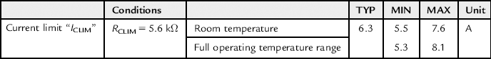
Now, if we are trying to get 5 A out of our converter with an r of 0.4, the estimated peak current will be 1.2×5=6 A. Clearly, as mentioned earlier, we are not going to get there with the LM2679! Unless we lower the value of r (increase inductance). Maximum value of r is
![]()
Solving, with IO=5 A, and ICLIM_MIN=5.3 A, we get
![]()
We can see from Figure 2.6, that this calls for an energy-handling capability (size of inductor) almost 3× the optimum!
Actually, it turns out that this part is just specified inappropriately. It in reality is the one with an adjustable current limit. And so, we could have probably adjusted the current limit adjust resistor quoted in the electrical tables to allow for a “better” value of current limit, and thereby a better value of r (at maximum rated load). But unfortunately, that is not clarified in the tables.
We should always remember that the minimum and maximum limits of the electrical tables are the only parts of a datasheet really guaranteed by any vendor (certainly not the typical values!). So, as a matter of fact, any other information in a datasheet just amounts to general design “guidance” — and that includes any “typical performance curves” provided. A prudent designer would never second-guess the vendor — in this case as to whether the current limit resistor can indeed be adjusted to give us a smaller inductor, or not. Therefore, as it stands, if we are using the LM2679 for a 5-A load current application, we do need an inductor three times larger than the optimum. Note that if the current limit could indeed be adjusted higher, the vendor should have picked the appropriate value for the current limit adjusted for a resistor in the “conditions” column of the electrical table (and declared the limits accordingly).
Note also that when we talk of a “5-A Buck IC,” it implies the part is supposed to deliver 5-A load current. The current limit of course needs to be set (and stated) correctly for the rated load, as discussed above. However, we should be very clear that when we are talking of Boost or Buck-Boost switcher ICs, a “5 A” part for example, does not give us a 5-A load current. That is because the DC inductor current is not equal to IO, but IO/(l−D) for these topologies. So, a “5-A” rating in this case only refers to the current limit of the device. What load current we can derive from a “non-Buck” IC depends on our specific application — in particular on the DMAX (duty cycle at VINMIN). For example, if the desired load current is 5 A, and the (maximum) duty cycle in our application is 0.5, then the average inductor current is actually IO/(l−D)=10 A. Further, with an r of 0.4, the peak would be 20% higher, that is, 1.2×10=12 A. So, for an optimum case, we would need to actually look for a device whose minimum current limit is 12 A or more in this case. At the bare minimum, we need a device with a current limit higher than 10 A, just to guarantee output power.
Continuous Conduction Mode Considerations in Fixing r
As discussed previously, under various conditions, we may enter discontinuous conduction mode (DCM). From Figure 2.5 we can see that just as DCM starts to occur, the current ripple ratio is 2. However, we can pose the question in the following manner — what if we have set the current ripple ratio to a certain value r′ (i.e., the current ripple ratio at the maximum load current, IO_MAX). And then we decrease the load current slowly — at what load does the converter enter DCM?
By simple geometry it can be shown that the transition to DCM will occur at r′/2 times the maximum load. For example suppose we set r′ to 0.4 at 3 A load, the converter will transition into DCM at (0.4/2)×3=0.6 A.
But designers know that when DCM is entered, a lot of things within the converter change suddenly! The duty cycle, for one, will now start pinching off toward zero as we decrease the load current further. In addition, the loop response of the converter (its ability to correct quickly for disturbances in line and load) also usually gets degraded in DCM. The noise and EMI profile can change suddenly too, and so on. Of course there are some advantages of operating in DCM too, but let us for now assume that for various reasons, the designer wishes to avoid DCM altogether, if possible.
We see that maintaining the converter in CCM, down to the minimum load of our application, enforces a certain maximum value for r′. For example, if the minimum load is IO_MIN=0.5 A, then to maintain the converter in CCM at 0.5 A, the set current ripple ratio (r′ at 3 A) needs to be lowered. Back calculating, we get the required condition for this
![]()
So,
![]()
In our case we get
![]()
We therefore need to set the current ripple ratio to less than 0.333 at maximum load, to ensure CCM at IO_MIN. This was the traditional design criterion for inductors, before Figure 2.6 was published and understood.
Note that generally speaking, we can make the converter operate in boundary conduction mode (BCM), or in full DCM, in three ways — (a) by decreasing the load, (b) choosing a small inductance, or (c) increasing the input voltage.
We realize that decreasing the load will proportionally decrease IDC to virtually any value, and so the condition r≥2 (BCM to DCM) will certainly occur sooner or later — below a certain load current. Similarly, decreasing L will necessarily increase ΔI, and so at some point we can expect the ratio ΔI/IDC (i.e., r) to try to become greater than 2 (implying DCM).
However, as far as the third method of entering DCM mentioned above is concerned, we should realize that solely increasing the input voltage just might not do the trick! DCM or BCM can only happen under an input (line) variation, provided the load current is simultaneously below a certain value to start with (the value being dependent on L).
It is instructive to study the three topologies separately in this regard. Note that the general equation for r is
![]()
Applying the voltseconds law in CCM (or BCM), we also get
![]()
(a) From the plots of r in Figure 2.4, we see that both the Buck and the Buck-Boost have the highest value of r when D approaches zero, i.e., at maximum input voltage. For these topologies, the equation for r (derivable from the more general equation for r just given immediately above) is
So, putting r=2 and D=0 (i.e., highest input voltage plus BCM), we get the limiting condition
![]()
Therefore, for these two topologies, if IO is greater than the above limiting value, we will always remain in CCM, no matter how high we increase the input voltage.
(b) Coming to the Boost, the situation is not so obvious. From Figure 2.4, we see that r peaks at D=0.33 (corresponding to the input being exactly two-thirds of the output). So, the Boost is most likely to enter DCM at D=0.33 — not say, at D=0 or D=1. We can derive the following (exact) equation for r
![]()
So, putting D=0.33, and r=2 in this equation, we get the following limiting condition
![]()
Therefore, for the Boost topology, if IO is greater than this value, we will always remain in CCM, no matter how high we increase the input voltage.
Note that, if we do manage to enter DCM, the most likely input point for this to happen is an input of 0.67 times the output. In other words, if we are not in DCM at this particular input voltage, we can be sure we will be in CCM throughout the entire input range (whatever it may be).
Setting r to Values Higher than 0.4 when Using Low-ESR Capacitors
Nowadays, with improvements in capacitor technology, we are seeing a new generation of very “low-ESR” capacitors — like monolithic multilayer ceramic capacitors (“MLCs” or “MLCCs”), polymer capacitors, and so on. Due to their extremely low ESRs, these capacitors usually have very high ripple (RMS) current ratings. Therefore, the required size of such capacitors in any application is no longer dictated by their ripple current handling capability. In addition, these capacitors also have almost no ageing characteristics (or lifetime issues) that we need to account for beforehand in the design (as we customarily do for electrolytic capacitors — which “dry out” over time). Further, due to their very high dielectric constant, these new capacitors have also become very small in size. So in fact nowadays, increasing r may not necessarily cause a noticeable increase in the space occupied by the capacitors (or size of converter). On the other hand, increasing r may still lead to a relatively significant reduction in size of the inductor.
Summing up, with modern capacitors to the rescue, it may start making perfect sense to increase r from its traditional “optimum” of 0.4, to say approximately 0.6–1 on occasion (provided other considerations do not restrict this). If we do so, Figure 2.6 tells us, we can still get an additional 30–50% reduction in the size of the inductor. And that is certainly not insignificant, provided of course that the advantage is not offset by having to use larger capacitors in the bargain (due to higher filtering capacitances required)!
Setting r to Avoid Device “Eccentricities”
Surprisingly, device eccentricities may on occasion play a part in defining the limits of r too. For example in Figure 2.8 we have presented the current limit plot of an integrated high-voltage flyback switcher IC called the “TOPSWITCH®.” On it we have superimposed a typical switch current waveform, just to make things a little clearer.
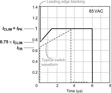
Figure 2.8: The “initial current limit” of the TOPSWITCH®.
We see that surprisingly, the current limit of this device is time-dependent for about 1.5 μs after the turn-on transition — something we don’t intuitively ever expect. This “initial current limit” of the device occurs just as its internal current limit comparator starts to come out of its (valid) “leading edge blanking” time. As mentioned, during this blanking time the IC is just “not looking” at the current at all to avoid spurious triggering on the noise edge of the turn-on transition. But the problem is that once the current limit circuit gets down to monitoring the switch current again, it takes a certain time for the current limit threshold to settle down — and during this time it can be triggered at only about 75% of the supposed current limit!
Looking at the switch (or inductor) current waveform, we know that the current at the moment the switch turns ON is always less than the average value by the amount ΔI/2. In other words, this trough (valley) current “ITR” is related to r according to the equation
![]()
We realize that to avoid hitting the initial current limit of the device, we need to ensure that the trough falls below 0.75×ICLIM. So,
![]()
Now, we are assuming the power supply is at maximum load in this analysis. Therefore, the peak current is set equal to the current limit ICLIM
![]()
Equating the above two equations, we get the limiting condition for r
![]()
![]()
Since r in any case is typically set to about 0.4, we should normally have no trouble with this “initial current limit” issue. However, note that on finer examination of the electrical tables of the datasheet, this 0.75×factor is specified only at 25°C. Unfortunately, very few power devices stay at 25°C for long! So, the bottom line is that, we, as designers, do not really know the value of the current limit as the device heats up. Yes, we can certainly make an educated guess, possibly leave an additional safety margin when fixing r, and certainly, we may face no problem whatsoever. But the truth is we are on our own now — the vendor has not provided the requisite data (in the form of guaranteed limits within the electrical tables).
Setting r to Avoid Subharmonic Oscillations
Looking at Figure 2.9, we see that in any converter, the output voltage is first compared against an internal reference voltage. Then, the difference between the two (the “error”) is filtered, amplified, and inverted by an “error amplifier,” the output of which (the “control voltage”) is fed to one of the two inputs of a “pulse width modulator” (PWM) comparator. On the other input of this PWM comparator, a ramp is applied, and this produces the switching pulses. So, for example, if the error at the output increases, the control voltage will decrease, and the duty cycle will thus decrease in an effort to reduce the output voltage. That is how regulation usually works.
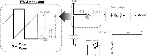
Figure 2.9: The pulse width modulator section of a power converter.
In voltage-mode control, the ramp applied to the PWM comparator is derived from an internal (fixed) clock. However, in current-mode control, it is derived from the inductor current (or switch current). And the latter leads to a rather odd situation where even a slight disturbance in the inductor current waveform can become worse in the next cycle (see upper half of Figure 2.10).
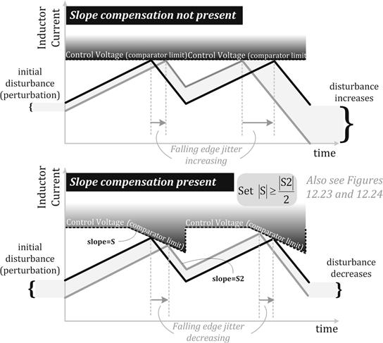
Figure 2.10: Subharmonic instability in current-mode control, and avoiding it by slope compensation.
Eventually, the converter may lapse into a strange “one pulse wide, one pulse narrow” switching waveform. This represents an operating mode that is definitely not “legitimate” or desirable for several reasons — in particular, the output voltage ripple is now much higher, and the loop response is severely degraded.
To get the disturbance to decrease every cycle and eventually die out, it can be shown that we need to do one of two things. Actually, both methods effectively amount to mixing a little voltage-mode control into current-mode control. So,
(a) either we add a small fixed (clock-derived) voltage ramp to the sensed voltage ramp (derived from the inductor/switch)
(b) or we subtract the same fixed voltage ramp from the control voltage (output of error amplifier)
As we can see from Figure 2.11, both are equivalent. That is in fact not surprising at all, considering that both the ramp and the control voltage go to the pins of a comparator. So, if we compare a signal A+B with a signal C, that is exactly equivalent to comparing A to C−B. And in both cases, equality at the input pins is established when A+B=C.
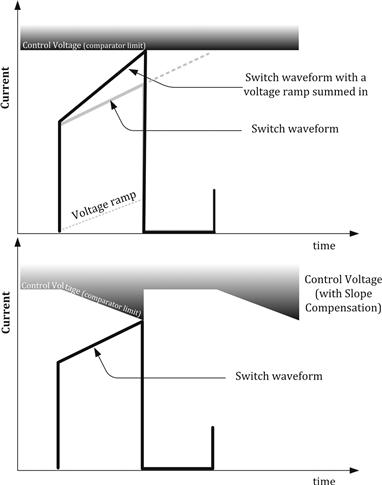
Figure 2.11: Adding a fixed ramp to the sensed signal, or modifying the control voltage, are equivalent methods of slope compensation in current-mode control.
This technique is called “slope compensation,” and is the most recognized way of quenching the alternate wide and narrow pulsing (or “subharmonic instability”) associated with current-mode control (see lower half of Figure 2.10). See also Chapter 12.
It can be shown that to avoid subharmonic instability, we need to ensure that the amount of slope compensation (expressed in A/s) is equal to half the slope of the falling inductor current ramp, or more. Note that in principle, subharmonic instability can occur only if D is (close to or) greater than 50%. So, slope compensation can be applied either over the full duty cycle range, or just for D≥0.5 as shown in Figure 2.10. Note that subharmonic instability can occur only if we are operating in continuous conduction mode (CCM). However, one way of avoiding this instability altogether is to operate in DCM.
If the amount of slope compensation is fixed by the controller, then as designers, we need to personally ensure that the slope of the falling inductor current ramp is equal to twice the slope compensation — or less (note that we are talking in terms of the magnitudes of the slopes only). This will in effect dictate a certain minimum value of inductance. And in terms of r, this tells us that we could have a situation where we may need to set r to less than the optimum of 0.4 — for example, if the control IC has an inadequate amount of built-in slope compensation.
As a result of more detailed modeling of current-mode control, optimum relationships for the minimum inductance required (to avoid subharmonic instability) have been generated as follows:
![]()
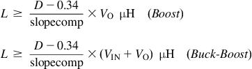
where the slope compensation is in A/μs.
Note that for all these topologies, we have to do the preceding calculation at the maximum input voltage point at which the duty cycle is greater than 50%, AND we are also simultaneously in CCM.
More details on subharmonic instability and slope compensation can be found in Chapter 12.
Quick Selection of Inductors Using “L×I” and “Load Scaling” Rules
Finally, having decided upon the value of r based on all the considerations outlined so far, we first present a quick method of picking an inductor for a given application. After that we will proceed to a more detailed analysis and worked example.
As mentioned previously, from the inductor equation V=L dI/dt, we can derive another useful relationship that we have named the “L×I” equation (“el-ex-eye” equation)
![]()
![]()
If we know the voltseconds (from our application conditions), and have a target value for r, we can calculate “L×I.” Then by knowing I, we can calculate L.
Note that L×I can be visualized as a sort of inductance “per” Ampere — except that the relationship is inverse — that is, if we increase the current, we need to decrease the inductance (by the same amount). So, for example, if we get an inductance of 100 μΗ for a 2-A application, then for a 1-A application, the inductance must be 200 μΗ, and for a 4-A application, the inductance would be 50 μΗ, and so on.
Note that because the L×I equation doesn’t depend on topology, switching frequency, or on the specific input/output voltages, we can graph it out universally, as in Figure 2.12. That helps quickly pick an inductance for any application. Let us now exemplify the L×I graphical selection method for each topology.
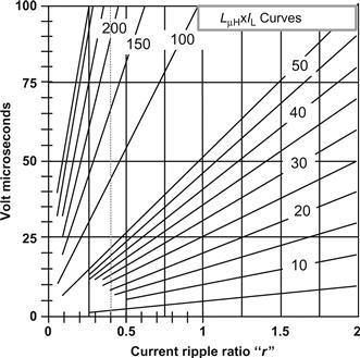
Figure 2.12: The “L×I” curves for quick selection of inductance.
Worked Examples (2, 3, and 4)
Buck: Suppose we have an input of 15–20 V, an output of 5 V, and a maximum load current of 5 A. What is the recommended inductance if the switching frequency is 200 kHz?
(a) We need to start the inductor design at VINMAX (20 V) for a Buck.
(b) The duty cycle from Table 2.1 is VO/VIN=5/20=0.25.
(c) The time period is 1/f=1/200 kHz=5 μs.
(d) The off-time tOFF is (1−D)×T=(1−0.25)×5=3.75 μs.
(e) The voltseconds (calculated using the off-time) is VO×tOFF=5×3.75=18.75 μs.
(f) From Figure 2.12, with r=0.4, and Et=18.75 μs, we get L×I=45 μΗ Α.
(g) For a 5 A load, IL=IO=5 A.
(h) Therefore, we need L=45/5=9 μΗ.
(i) The inductor must be rated for at least (1+r/2)×IL=1.2×5=6 A.
Summarizing, we need a 9 μΗ/6 A inductor (or closest available).
Boost: Suppose we have an input of 5–10 V, an output of 25 V, and a maximum load current of 2 A. What is the recommended inductance if the switching frequency is 200 kHz?
(a) We need to start the inductor design at VINMIN (5 V) for a Boost.
(b) The duty cycle from Table 2.1 is (VO−VIN)/VO=(25−5)/25=0.8.
(c) The time period is 1/f=1/200 kHz=5 μs.
(d) The on-time tON is D×T=0.833×5=μs.
(e) The voltseconds (calculated using the on-time) is VIN×tON=5×4=20 μs.
(f) From Figure 2.12, with r=0.4, and Et=20 μs, we get L×I=47 μΗ Α.
(g) For a 2 A load, IL=IO/(1−D)=2/(1−0.8)=10 A.
(h) Therefore, we need L=47/10=4.7 μΗ.
(i) The inductor must be rated for at least (1+r/2)×IL=1.2×10=12 A.
Summarizing, we need a 4.7 μΗ/12 A inductor (or closest available).
Buck-Boost: Suppose we have an input of 5–10 V, an output of −25 V output, and a maximum load current of 2 A. What is the recommended inductance if the switching frequency is 200 kHz?
(a) We need to start the inductor design at VINMIN (5 V) for a Buck-Boost.
(b) The duty cycle from Table 2.1 is VO/(VIN+VO)=25/(5+25)=0.833.
(c) The time period is 1/f=1/200 kHz=5 μs.
(d) The on-time tON is D×T=0.833×5=4.17 μs.
(e) The voltseconds (calculated using the on-time) is VIN×ION=5×4.17=20.83 μs.
(f) From Figure 2.12, with r=0.4, and Et=20.83 μs, we get L×I=52 μΗ Α.
(g) For a 2 A load, IL=IO/(1−D)=2/(1−0.833)=12 A.
(h) Therefore, we need L=52/12=4.3 μΗ.
(i) The inductor must be rated for at least (1+r/2)×IL=1.2×12=14.4 A.
Summarizing, we need a 4.3 μΗ/14.4 A inductor (or closest available).
The Current Ripple Ratio r in Forced Continuous Conduction Mode (“FCCM”)
Finally, before we move on to magnetic fields, we make some closing remarks on designing with forced continuous conduction mode (“FCCM”). More on this in Chapter 9.
As discussed previously, r is defined only for CCM, and therefore cannot exceed 2 (since that marks the boundary between CCM and DCM). However, in synchronous regulators (with diode replaced or supplemented by a low-drop MOSFET across it), we actually never enter DCM (unless the IC is deliberately designed to go into “diode emulation mode”). So now, on decreasing the load, we actually continue to remain in CCM. That is because for DCM to ever occur, the inductor current must be forced to stay at least for some part of the switching cycle at zero. And to get that to happen, we need to have a reverse-biased diode that prevents the inductor current from “going the other way.” But in synchronous regulators, the MOSFET across the diode allows reverse-conduction even if the diode is reverse-biased, so we do not get DCM.
The CCM-type mode that replaces the DCM mode in synchronous regulators is distinguished from the usual (normal) CCM mode, by calling it the “forced continuous conduction mode” (FCCM). The main switch is usually identified as the top (or “high-side”) MOSFET, whereas the MOSFET across the diode is called the bottom (or “low-side”) MOSFET. Further, in FCCM, r is legitimately allowed to exceed 2 (see Figure 2.5).
We can visualize FCCM as starting to occur when the load current is decreased sufficiently to cause part of the inductor current waveform to become “submerged” below “sea-level” — that is, with parts of it having a negative value (inductor current flowing momentarily away from the load). But note that as long as we are still drawing some load current out of the output terminals of the converter, the average value of the waveform, IDC (center of ramp), is still positive — that is, going toward the load — on an average. Further, because IDC is always proportional to the load current, it can be made to decrease all the way down to zero while still maintaining CCM. Since the swing in current, ΔI, depends only on the input and output voltages, which we have assumed have not changed, the ratio r=ΔI/IL not only exceeds 2 but can in fact become extremely large.
All the basic design equations we can write for the RMS, DC, AC, or peak currents in the input/output capacitors and the switch, when operating in conventional CCM, apply to the converter in FCCM too (though there may be some additional losses, as for example when the current flows through the body diode of the top MOSFET). This, despite the fact that r can now exceed 2. In other words, the CCM equations do not get invalidated in FCCM. However, a specific computational problem can arise in some cases, because if r is infinite (zero load current), we can get a singularity — a “0” in the denominator. At first sight, this seems to make the CCM equations (presented the way we have been doing) unusable. But, one trick that can be employed to avoid the singularity is to assume a few milliamperes of minimum load, however small. Alternatively, we can substitute r=ΔI/IDC back into the equations, and we will then see that IDC cancels out (does not appear in the denominator anywhere). Either way, the equations of CCM (see the Appendix), apply to FCCM too.
Basic Magnetic Definitions
Having understood basic concepts like voltseconds, current components, worst-case voltage, and also how to do an initial (quick) selection of an off-the-shelf inductor, we will now try to go inside the magnetic component, so as to learn what happens in terms of the magnetic fields present inside its core. We will then use this information to do a more complete validation of a selected off-the-shelf inductor. Then we will find the remaining (worst-case) stresses of the converter.
At the outset, we should note that in magnetics, there are several different systems of units in use. This can become very confusing, since even the basic equations look different depending on the system in use. It is therefore a wise policy to stick to one system of units all the way through — converting to a different system, if required, only at the very end, that is, only at the level of numerical results (not at the level of equations).
Further, unless otherwise stated, the reader can safely assume we are using the meter–kilogram–seconds system of units — that is, “MKS” system, also called the “SI” system (for System International).
The basic definitions are as follows:
• H-field: Also called “field strength,” “field intensity,” “magnetizing force,” “applied field,” and so on. Its units are A/m.
• B-field: Also called “flux density” or “magnetic induction.” Units of B are Tesla (“T”) or Webers per square meter (Wb/m2).
• Flux: This is the integral of B over a given surface area expressed as Webers (Wb). It is
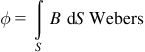
where dS is a differential of surface area. If B is constant over the surface, we get the more common form ϕ=BA, where A is the area of the surface through which the flux in question is flowing.
Note: The integral of B over a closed surface is zero since flux lines do not start or end at any given point but are continuous.
• B is related to H at any given point by the equation B=μΗ, where μ is the permeability of the material. Note that later we will use the symbol μ for “relative permeability,” that is, the ratio of the permeability of the material to that of air. So, in MKS units we should actually preferably write B=μcΗ, where μc is the permeability of the core (magnetic material). By definition, μc=μμo.
• The permeability of air, denoted by μο, is equal to 4π×10−7 Henrys/m in MKS units. In CGS units it is equal to 1. That is why in CGS units μc=μ, where μ is also automatically the relative permeability of the material (though units are different).
• Faraday’s law of induction (also called Lenz’s law) relates the induced voltage V that is developed across the ends of a coil (N turns), to the (time varying) B-field passing through it. So,
![]()
• The “inertia” of a coil to a change in flux through it due to a time-varying current through it is its “inductance” L, defined as
![]()
• Since it can be shown that the flux is proportional to the number of turns N, the inductance L is proportional to the square of the number of turns. This proportionality constant is called the “inductance index” and is denoted by “AL.” It is usually expressed as nH/turns2 (though sometimes it is considered to be mH/1,000 turns2, both being numerically the same). So,
![]()
• When H is integrated over a closed loop, we get the current enclosed by the loop
![]()
where the integration symbol above reflects the fact that it is being performed over a closed loop. This is also called “Ampere’s circuital law.”
• Combining Lenz’s law with the inductor equation V=L dI/dt, we get
![]()
• From this we get the two key equations used in power conversion
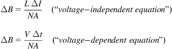
The first equation can be written symbolically as
![]()
And the latter equation can be written in a more “power-conversion-friendly” form as follows
![]()
For most inductors used in power conversion, if we reduce the current to zero, the field inside the core also goes to zero (not a permanent magnet). An implicit assumption of complete linearity is also usually made — that is, B and I are considered proportional to each other as shown in Figure 2.13 (unless of course the core starts saturating, at which point, all bets are off!). The voltage-independent equation can then be expressed as any of the equations shown in the figure — in other words, this proportionality applies to the peak values of current and field, their average values, their AC values, their DC values, and so on. The constant of proportionality is equal to
![]()
where N is the number of turns and A the actual geometrical cross-sectional area of the core (its center limb usually, or simply the “effective area” Ae given in the datasheet of the core). See Chapter 5 too.
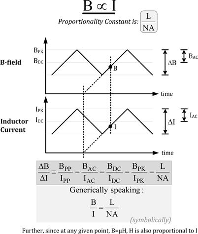
Figure 2.13: B and I can be usually considered to be proportional to each other.
Worked Example (5) — When Not to Increase the Number of Turns
Note that the voltage-independent equation is useful if, for example, we want to do a quick check to see if our core may be saturating. Suppose we are custom-designing our inductor. We have wound 40 turns on a core with an area of A=2 cm2. Its measured inductance is 200 μΗ, and the peak inductor current in our given application is 10 A. Then the peak flux density can be calculated as follows:
![]()
Note that we have converted the area to m2 in the above equation, because we are using the MKS version of the equation.
For most ferrites, an operating flux density of 0.25 T is acceptable, since the saturation flux density is typically around 0.3 T.
Based on the B and I linearity, we can also linearly extrapolate and thus conclude that the peak current in our application should under no condition be allowed to exceed (0.3/0.25)×10=12 A, because at 12 A, the field will be 0.3 T, and the core will then start to saturate.
But note that the number of turns should not be increased any further (at 12 A). Looking at the ΒPK equation above, it seems at first sight that increasing the number of turns will reduce the B-field. However, inductance increases as N2 (from the AL equation given previously); so, the numerator will increase much faster than the denominator. Therefore, in reality, the B-field will increase, rather than decrease if we increase the number of turns, and we know we can’t afford to exceed 0.3 T.
In other words — we usually tend to instinctively rely on the current-limiting properties of an inductor. And in general, increasing the inductance will certainly help increase the inductance, and therefore help limit the current. However, if we are already close to the energy-storage limits of the material of the core, we have to be very careful — a few extra turns could take us “over the edge” (saturation), and then in fact, the inductance will start collapsing rather than increasing.
We should also not forget our basic premise of inductors in power conversion — for a given application, a large inductance does usually end up requiring a large inductor! So, increasing the number of turns, without increasing the size, may naturally turn out to be a recipe for disaster.
The “Field Ripple Ratio”
Since I and B are proportional to each other, and r happens to be a ratio, we realize that r must apply equally to the field components as it does to the current components. So, in that sense, r can be looked at as a “field ripple ratio” too. We can therefore extend the definition of r as follows
![]()
Therefore, r can also be used to relate the peak, AC, and DC values of both the current and field according to the equations
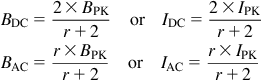
We can relate the peak to the swing too as follows:
![]()
The latter form will in fact be used later by us in a worked example that follows.
The Voltage-Dependent Equation in Terms of Voltseconds (MKS Units)
When discussing the current swing ΔI, we related it to the voltseconds. Now we can do the same for the B-field
![]()
So as for current, the voltseconds in our application also determines the swing of the magnetic field — though not its DC level.
CGS Units
We may personally prefer to use the more broadly accepted MKS units, but we have to deal with the ground reality of the situation — that certain vendors (especially North American ones) still use “CGS” (centimeter-gram-seconds) units. Since we would certainly be evaluating and looking at their datasheets too, we will need to use the conversions in Table 2.4.
Table 2.4. Magnetic Systems of Units and Their Conversions.
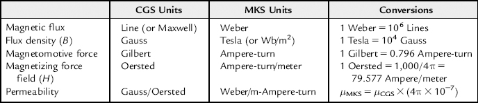
In particular, we should remember that the saturation flux density BSAT, which is around 0.3 T (300 mT) for most ferrites, is 3,000 Gauss (“G”) in CGS units. Also note that permeability of a material in MKS units needs to be divided by 4π×10−7 to get the permeability in CGS units. The reason for that is that permeability of air is set to 1 in CGS units, but in MKS units it is (numerically) equal to 4π×10−7.
The Voltage-Dependent Equation in Terms of Voltseconds (CGS Units)
It is also therefore helpful to know how to write the voltage-dependent equation (expressed in terms of Et) in CGS units instead.
So, converting A in m2 to A in cm2, we get from the previous equation
![]()
Core Loss
The core loss depends on various factors — the flux swing ΔΒ, the (switching) frequency f, and the temperature (though we usually ignore this latter dependency for most estimates). Note however, that when vendors of magnetic materials express the dependency of core loss on a certain “ B,” what they are really talking about is ΔΒ/2, that is, BAC. This happens to be the usual industry convention, but it is often quite confusing to power supply designers. In fact, there is more confusion caused by the fact that “B” may be expressed by the vendor, either in terms of Gauss or in Tesla. In fact, the dissipation also (due to the core loss) may be expressed either as mW or as W.
First, let us look at the general form of core loss.
![]()
where “core loss per unit volume” is expressed generally as
![]()
In Table 2.5 we have indicated the three main systems of units in use for describing the core loss per unit volume, and also provided the rules for converting between them. Note that we are using “Ve” (effective volume) here — this usually can be considered as the actual physical volume of the core, or we can just look it up in the datasheet of the core.
Table 2.5. The Different Systems in Use for Describing Core Loss (and Their Conversions).
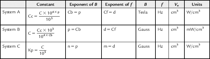
In Table 2.6, we have provided values for the constants in the core loss equation in one of these systems of units, besides some other operating limits. The reader is however advised to confirm these values from the respective vendors.
Table 2.6. Typical Core Loss Coefficients of Common Materials.
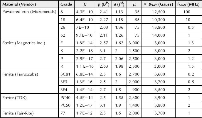
Note: (a)E–(b) is (a)×10−(b)
Worked Example (6) — Characterizing an Off-the-Shelf Inductor in a Specific Application
Now we will present the “general inductor design procedure” we have been talking about. We will be considering a wide-input voltage range here. The procedure is to be carried out at the “worst-case input voltage end” with respect to the peak current. The basic purpose is to ensure that we are avoiding inductor saturation under normal operation. So for the Buck, we will work at VINMAX, because that is the point at which the peak current is at its maximum. For a Boost or a Buck-Boost, we need to conduct this procedure at VINMIN, not VINMAX, since that is the worst-case input voltage end with regard to the peak current, for these topologies.
The procedure will be illustrated by means of a step-by-step worked example. Though it is carried out for a Buck, throughout the calculation, we will indicate precisely how the procedure and equations may need to change, were this a Boost or a Buck-Boost. So for example, to the right of any equation presented below, we have indicated in brackets, which topology it is valid for.
A Buck converter has an input of 18–24 V, an output of 12 V, and a maximum load of 1 A. We desire a current ripple ratio of 0.3 (at maximum load). We assume VSW=1.5 V, VD=0.5 V, and f=150,000 Hz. An off-the-shelf inductor is to be selected and characterized for this application.
As mentioned, all the steps involved in the “general inductor design procedure” below are being carried out at a certain “VIN” — which is the maximum input voltage for a Buck, and minimum input voltage for a Boost or a Buck-Boost.
Estimating Requirements
For a Buck regulator, the duty cycle is (now including the switch and diode forward drops)
![]()
![]()
(For Boost, use ![]() , for Buck-Boost, use,
, for Buck-Boost, use, ![]() )
)
The switch on-time is therefore
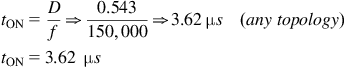
The voltage across the inductor when the switch is ON is
![]()
(For Boost and Buck-Boost, use VON=VIN−VSW.)
So, the voltsmicroseconds is
![]()
Using the “L×I” equation
![]()
we get
![]()
But the average inductor current is
![]()
(For a Boost and Buck-Boost, use ![]() .)
.)
Therefore,
![]()
The peak current will be 15% higher than IL for r=0.3. This follows from
![]()
We now pick a promising off-the-shelf inductor — the PO150 from Pulse Electronics. Its inductance is 137 μΗ, which is close to our requirement of 127 μΗ, and it is rated for a continuous DC of 0.99 A, which is very close to our requirement of 1 A. Its datasheet is reproduced in Table 2.7. Note that the other conditions mentioned by the vendor do not match our application (but that is not unexpected — what are the chances of an off-the-shelf inductor that precisely matches a given application?). Nevertheless, we can perform a full analysis, and thus either validate or invalidate our choice of component.
Table 2.7. Specifications of a Selected Inductor (the PO150).
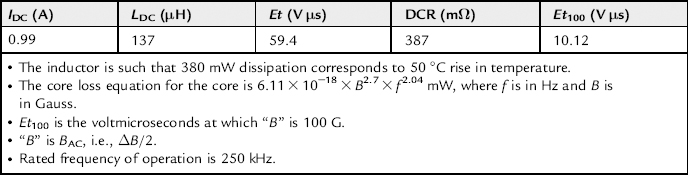
Current Ripple Ratio
We use the “L×I” rule
![]()
So,
![]()
The inductor has been designed by its vendor, for an r of
![]()
In our application we will get
![]()
This is very close to (and less than) our target of r=0.3, and is therefore acceptable.
Peak Current
The inductor has been designed for a peak current of
![]()
In our application we will get
![]()
The peak current in our application is considered “safe,” being less than what the inductor was originally designed for. Therefore, we can safely assume that the peak B-field of our application must also be within the design limits of the inductor. However, it is instructive to confirm that directly, as we do next.
Note that the frequency has not even entered the picture directly so far, since voltseconds is all that really matters to an inductor. Different applications, with the same DC level of current, and the same voltseconds, are essentially the same application from the viewpoint of the inductor. It just “doesn’t care,” for example, what topology it is, or what is the duty cycle. It doesn’t even care about the frequency directly (though the exception to this is the core loss term, because that depends not only on the voltseconds, i.e., the current swing, but on the frequency too). However, we will also see that the core loss term is much smaller anyway, compared to the copper loss. So, for all practical purposes, if the rated voltseconds of a given inductor (current swing), and its DC current rating correspond to the applied voltseconds and DC current of our application, we are almost certainly going to be fine right off-the-bat. However, even if the rated voltseconds and DC level are quite different, as long as the applied peak flux density is close to or less than the rated value, we are OK from the saturation point of view. That’s a good start, and we can then proceed to do a full validation analysis — of the temperature rise and so on, under our specific application conditions.
Flux Density
The vendor provides the following information (see Table 2.7):
![]()
This means that the voltμseconds that produces a BAC of 100 G is 10.12. Since BAC=ΔΒ/2, the corresponding ΔΒ is 200 G (for every 10.12 V μs). Note that G stands for Gauss.
We had previously presented the following relationship between ΔΒ and Et:
![]()
Since ΔΒ and Et are proportional to each other (for a given inductor), we can conclude that the inductor has been designed for a flux density swing of
![]()
and a peak flux density of
![]()
In our application this will give us a swing of
![]()
and a peak of
![]()
We see that the peak field in our application is within the design limits of the inductor, as expected, so we need not worry about core saturation. This is a basic qualification the inductor must pass before we can proceed with the rest of the analysis.
Note that the proportionality constant connecting B and I (for this inductor) is
![]()
Note: If we break open the inductor and measure the number of turns, and also estimate/measure the cross-sectional area of the central limb of its core, we can verify the number 2,708 above.
Copper Loss
From the equations contained in Figure 2.14, we can calculate the RMS of the inductor current waveform. The inductor was designed for an RMS squared of
![]()
and a copper loss of
![]()
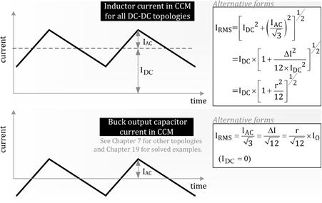
Figure 2.14: RMS value of the inductor current waveform.
Whereas in our application we will get
![]()
and a copper loss of
![]()
Core Loss
Note that the vendor has already factored in the volume of the core and thus provided the following overall equation for the core loss of the inductor:
![]()
where f is in Hz and B is in Gauss. Note that “B” is ΔΒ/2 here as per convention. So, the core loss that the inductor was originally designed for is
![]()
Whereas in our application
![]()
DC–DC Converter Design and Magnetics
In general, we will find that in most ferrite-based off-the-shelf inductors, the designed core loss is only 5–10% of the total inductor loss (copper-plus-core loss). However, if the inductor uses a “powdered iron” core, this number may rise to about 20–30%.
Note: Powdered iron cores tend to saturate more “softly” than ferrites, and that usually enhances their ability to withstand severe abnormal currents without leading to immediate switch destruction. On the other hand, powdered iron cores may have “lifetime” issues caused by slow degradation of the organic binder that holds their iron particles together. The vendor must be consulted about this possibility, and the steps necessary to avoid a premature end to our converter!
Temperature Rise
The vendor has stated that the inductor is such that 380 mW dissipation corresponds to 50°C rise in temperature. In effect this tells us that the thermal resistance of the core “Rth” is
![]()
The inductor was originally designed for a total loss of
![]()
This would have given a temperature rise of
![]()
In our application
![]()
This will give a temperature rise of
![]()
Provided we accept this temperature rise in our application (that will depend on our maximum operating ambient temperature), we can validate the chosen inductor. We have already confirmed it does not saturate in our application, and further, the current ripple ratio it provides is acceptable too.
Calculating “Other” Worst-case Stresses and their Selection Criteria
Having validated our choice of inductor, we can look a little more closely at the important issue of how the wide-input range impacts the other key parameters and stresses in our proposed converter. This also helps in correctly selecting the other power components.
Worst-case Core Loss
In the above so-called “general inductor design procedure,” we have actually been working at VINMAX for a Buck, and at VINMIN for a Boost or Buck-Boost. The reason was that the inductor sees the highest peak current at this voltage end, so we have to “ensure” the magnetics design at these particular points (extremes). But this point may not be the worst-case for the other stresses in the power supply, and we need to start understanding that clearly now.
Let us first focus on the inductor. The point at which we are doing the inductor design usually gives us the worst-case temperature rise too. But that is because the IDC component of the inductor current is usually the dominant term. If for any reason, we are interested in knowing what the maximum core loss component of the total loss is, we should realize, looking back at Figure 2.4, that though the DC level may be going up as input voltage falls, the AC component (on which the core loss term depends) may actually be decreasing (or having an odd-shaped profile, as for the Boost).
From Figure 2.4, we see that IAC increases at high-input voltages for both the Buck and the Buck-Boost, but not necessarily for the Boost. For a Buck, the general inductor design calculation above was carried out at VINMAX and that just happens to be the point at which the core loss is a maximum too. Therefore, calculating the core loss at VINMAX as we did in the previous example does coincidentally also give us the worst-case core loss.
However, if we were doing the calculation for a Buck-Boost, our general inductor design calculation starts at VINMIN. But the core loss is a maximum at VINMAX. Similarly, for a Boost, we would also start the general inductor design calculation at VINMIN. But the worst-case core loss for this topology actually occurs at D=0.5 (see the IAC curve for Boost in Figure 2.4). Note that from the duty cycle equation of Boost, D=0.5 corresponds to an input voltage equal to half the output.
Note: If for the Boost, the input range of the given application does not include the D=0.5 point, we need to identify which voltage end of the range provides a duty cycle closest to D=0.5. And we need to then do the worst-case core loss calculation at that end. That would be the input voltage extreme with a D closest to D=0.5.
Generally, the core loss term, being such a small component of the total loss, is of no great concern to us, so we won’t even bother to do a numerical calculation here. But the general procedure to handle such cases will become apparent as we study the other worst-case loss terms of the converter below.
First let us start annotating (or subscripting) some of the terms derived so far, just for gaining clarity in the discussion to follow.
• For a Buck: The general inductor design procedure was carried out at VINMAX, that is, DMIN. So for example, the r we have set to 0.3–0.4 (and possibly re-calculated with the selected inductor) is now referred to as “rDMIN.” Similarly, the voltseconds, Et, we have calculated so far is actually “EtDMIN.”
• For a Boost and Buck-Boost: If a similar general inductor design procedure were carried out for these topologies, it would be done at VINMIN that is, DMAX. So for example, the r we would have set to 0.3–0.4 (and possibly re-calculated with the selected inductor) would actually be called “rDMIN.” Similarly, the voltseconds, Et, we would have calculated so far is “EtDMIN.”
We need to keep these distinctions in mind, otherwise the following discussion can become confusing no end!
Worst-case Diode Dissipation
The general equation for the average diode current is
![]()
or equivalently
![]()
This leads to a diode dissipation of
![]()
For the Buck, as the input voltage is raised, the duty cycle falls, and because the average inductor current IL remains fixed at IO, the average diode current increases. That means we get the worst-case diode current (and dissipation) at VINMAX for a Buck. Therefore, we can just use the numbers already derived while carrying out the general inductor design procedure (at VINMAX).
For the Boost and the Buck-Boost, as the input is raised, D decreases, but the average inductor current also falls, thereby keeping ID fixed at IO. (We should remember that the Boost and the Buck-Boost are unique in the sense that all the output current must pass through the diode when it conducts, so ID must necessarily equal IO at all times.) That means the diode dissipation is independent of input voltage for these topologies. So we can, if we want, just use the numbers already derived while carrying out the general inductor design procedure (at VINMIN).
Finally, for the ongoing Buck converter design example, the calculation is as follows:
![]()
Note that the General Diode Selection Procedure is as Follows
The rule of thumb is to pick a diode with a current rating at least equal to, but preferably at least twice the worst-case average diode current given below (for low losses, since the diode forward drop decreases substantially if its current rating is increased):
Its voltage rating is usually picked to be at least 20% higher (“~80% derating” — i.e., safety margin) than the worst-case diode voltage given below:
Worst-case Switch Dissipation
For all topologies the average input current (and therefore switch current) must increase as the input voltage decreases, so as to continue to satisfy the basic power requirement expressed by PIN=IIN×VIN=ΡΟ/η (where η is the efficiency, assumed fixed). Therefore, the switch RMS current is a maximum at VINMIN (i.e., DMAX) for all topologies.
For the Boost and Buck-Boost, the general inductor design procedure is at DMAX in any case. So, we can directly use the numbers derived from that to find the switch RMS current using the equation below:
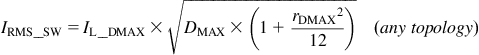
where IL_DMAX and rDMAX are, respectively, the average inductor current and current ripple ratio at DMAX (i.e., at VINMIN). DMAX can be calculated using
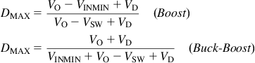
and we should remember that
![]()
For the Buck, the general inductor design procedure is at DMIN. So, we cannot directly use the numbers derived from that to find the switch RMS current (by the previously given equation). We need to calculate rDMAX, but we only know tDMIN so far. Let us proceed with the required steps.
![]()
In other words, if we know the voltseconds at VINMIN, we will know the corresponding current ripple ratio rDMAX for the chosen inductor. But first we have to calculate DMAX
![]()
The switch on-time is therefore
![]()
The voltage across the inductor when the switch is ON is
![]()
So, the voltmicroseconds is
![]()
Therefore,
![]()
Finally, we are in a position to calculate the switch dissipation

If, for example, the Drain-to-Source resistance is 0.5 Ω, the dissipation in the MOSFET is
![]()
Note that the General Switch Selection Procedure is as Follows
The rule of thumb is to pick a switch with a current rating at least equal to, but preferably at least twice the worst-case RMS switch current calculated above (for low losses, since the switch forward drop will decrease substantially if its current rating is increased).
Its voltage rating is usually picked to be at least 20% higher (“~80% derating” — i.e., safety margin) than the worst-case switch voltage given below:
Worst-case Output Capacitor Dissipation
Coincidentally, the worst-case output capacitor RMS current for all three topologies occurs at the same point at which the general inductor design procedure for each of them is carried out. In other words, this point is VINMAX for the Buck, and VINMIN for the Boost and Buck-Boost. So, we should have no trouble, directly using the numbers derived from the general inductor design procedure, to find the worst-case RMS current of the output capacitor, using the equations below:
For the Buck, we get
![]()
So for example, if the ESR of the output capacitor is 10 Ω, we get the dissipation
![]()
For the Boost and the Buck-Boost, we need to use
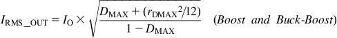
Note that the General Output Capacitor Selection Procedure is as Follows
The rule of thumb is to pick an output capacitor with a ripple current rating equal to or greater than the worst-case RMS capacitor current calculated above. Its voltage rating is usually picked to be at least 20–50% higher than what it will see in the application (i.e., VO for all topologies). The output voltage ripple of the converter is also usually a concern. The total peak-to-peak output voltage ripple produced by the output capacitor is equal to its ESR multiplied by the worst-case peak-to-peak output current given below (ignoring the ESL of the capacitor):
• For a Buck — peak-to-peak capacitor current is IO×rDMIN. This is the same point at which the general inductor design procedure would have been carried out, and so rDMIN is already known.
• For a Boost — peak-to-peak capacitor current is IO×(1+rDMAX/2)/(1−DMAX). This is the same point at which the general inductor design procedure would have been carried out for this topology, so rDMAX and DMAX are already known.
• For a Buck-Boost — peak-to-peak capacitor current is IO×(1+rDMAX/2)/(1−DMAX). This is the same point at which the general inductor design procedure would have been carried out for this topology, so rDMAX and DMAX are already known.
Worst-case Input Capacitor Dissipation
For the Buck-Boost, things are much simpler, since the worst-case input capacitor RMS current occurs at DMAX, which is also the point at which we carry out the general inductor design procedure. So, all the numbers available from that procedure can be used directly in the equation below:
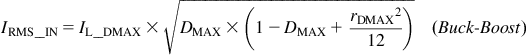
For the Buck and the Boost, the worst-case input RMS capacitor current occurs at D=0.5. Therefore, we have to calculate “r50,” that is, the current ripple ratio at D=50% (or whatever voltage within the specified input range of our application range is closest to this point).
Let us do the numerical calculation for the Buck, and the procedure will become clearer.
The input voltage at which D=50% occurs for the Buck is
![]()
and for the Boost
![]()
We see that our input range does not include this point. But the closest to it is VINMAX. However, coincidentally, this is already the point at which the general inductor design procedure was carried out. So, we can use all the numbers derived from that procedure to calculate the input capacitor RMS current, using the equation below:

and for the Boost
![]()
So finally
![]()
Note: If for our worked Buck example, the input range was not 18–24 V but say 30–45 V, then the general inductor design procedure would clearly be carried out at 45 V. However, the input capacitor current would be a maximum at 30 V. So, we can use the above equation for the RMS current, but we would now need to use rDMIN and DMAX. Therefore, knowing only rDMAX so far we would need to calculate rDMIN by the same procedure presented earlier — that is, by recalculating the voltseconds, and so on.
A full solved example is available in Chapter 19. See also Chapters 6 and 7 for stress derivations and sample calculations.
Note that the General Input Capacitor Selection Procedure is as Follows
The rule of thumb is to pick an input capacitor with a ripple current rating equal to or greater than the worst-case RMS capacitor current calculated above. Its voltage rating is usually picked to be at least 20–50% higher than what it will see in the application (i.e., VIN_MAX for all topologies). The input voltage ripple of the converter is also usually a concern because a small part of it does get transmitted to the output. There can also be EMI considerations involved. In addition, every control IC has a certain (usually unspecified) amount of input noise and ripple rejection, and it may misbehave if the ripple is too much. Typically, the input ripple needs to be kept down to less than ±5% to ±10% of the input voltage. The total peak-to-peak input voltage ripple produced by the input capacitor is equal to its ESR multiplied by the worst-case peak-to-peak input current given below (ignoring the ESL of the capacitor):
• For a Buck — peak-to-peak capacitor current is IO×(1+rDMIN/2). This is the same point at which the general inductor design procedure would have been carried out, and so rDMIN is already known.
• For a Buck-Boost — peak-to-peak capacitor current is IO×(1+rDMAX/2)/(1−DMAX). This is the same point at which the general inductor design procedure would have been carried out for this topology, so rDMAX and DMAX are already known.
• For a Boost — peak-to-peak capacitor current at the worst-case point for this parameter (i.e., D=0.5) is equal to 2×IO×r50 where
![]()
Note that if the input range does not include the D=0.5 point, we need to look for the input voltage end closest to D=0.5. Then we can use the general equation for the peak-to-peak input capacitor current
![]()
where r and D correspond to this particular worst-case input voltage end. To find r we can use
![]()
where L is in H, and f is in Hz.
That completes the converter and magnetics design procedure. Next we will move on to off-line converters.
For further clarification on the techniques introduced in this admittedly tricky chapter, please refer to Chapters 6, 7 and 19 later.