
Chapter 6
Component Ratings, Stresses, Reliability, and Life
This chapter is an overview of the concepts behind electrical, thermal, and mechanical stresses in power conversion. The corresponding best practices and trade-offs in component selection and design so as to achieve realistic reliability targets in commercial designs is discussed. The emerging power conversion standard, IPC-9592, is introduced. Part 1 of the chapter focuses on developing a thorough understanding of power component ratings underlining which of those ratings are relevant and/or potentially called into question in different locations inside a power converter. The relevance of topology is also highlighted alongwith ways to avoid over-design. Part 2 goes into stress derating principles and the calculation and estimation of failure rates, life expectancy, and MTBF. Demonstrated reliability testing using Chi-square tables and reliability predictions based on the philosophy of MIL-HDBK-217F are presented. Accelerated life/stress testing and HALT and HASS are explained. Warranty costs calculations are provided. Part 3 concludes this chapter with a detailed analysis of life estimates of aluminum electrolytic capacitors.
Introduction
In Chapter 5, we looked at the selection and design of the magnetic components. Our strategy was straightforward. First, we examined different topologies and applications and understood what their requirements were in terms of energy. Then we studied the energy capabilities of different cores with varying materials, geometries, volumes, and air gaps. Thereafter, we proceeded to match requirements to capabilities. In this chapter and in the next, we look at the other power components involved, and try to understand how to select them using the same basic “match-making” approach. However, there is a slight difference. This time, our focus is not on energy storage, but on stresses. Stresses form one of the major selection criteria of the non-magnetic power components, the switch, diode, and input/output capacitors. Here is what we need to know as we go down that path.
(a) Using a mechanical analogy, we have to make sure that at a minimum, the strength (rating) of the part exceeds the worst-case force (stress) applied to it in a given application, or else, the part could “break” (fail). The strength of the part may vary significantly over production lots, environmental conditions (like temperature and humidity), perhaps even over time (degradation/aging). However, the lowest (worst-case) strength is typically guaranteed by the vendor/manufacturer of the part. For example, a discrete MOSFET comes with Absolute Maximum (“Abs Max”) ratings for its Drain-to-Source voltage (VDS), and its Gate-to-Source voltage (±VGS). Usually we cannot exceed the Abs Max rating even for a moment, without risking immediate damage. We should note that the Abs Max rating is a maximum stress level, not a performance rating. Performance is also guaranteed by the datasheet via electrical characteristics tables, up to a certain upper performance level slightly below the Abs Max level. For example, in a typical switcher or PWM controller IC, that upper performance level is referred to as its maximum operating voltage.
(b) Further, we need to ensure the components are able to adequately handle the stresses appearing across them over all operating corners of the given application. Unfortunately, especially in switching power converters, that worst-case point is not always obvious. We may need a careful pre-study to discover that. This eventually leads us to the “Stress Spider” in Chapter 7.
(c) Eventually, we also want to ensure that some safety margin should be present. This margin may be slim for commercial products, but very generous for medical, military, or “high-rel” (high-reliability) products. Note that in electrical terminology, safety margin becomes “derating,” Derating is a concept we had briefly discussed in Chapter 1. Now we take that discussion further.
Stresses and Derating
As power supply designers we conform to a certain “Stress Factor” defined as
![]()
The word “Design Margin” is also often used, and refers to the reciprocal of the Stress Factor. For example, a Design Margin of 2 means a Stress Factor of 0.5 (50%). “Margin of Safety” (or just Safety Margin) is formally
![]()
where Design Margin=strength/stress.
As a rough initial guideline, a Stress Factor of about 80% is considered to be a general design target in commercial applications. That gives us 1 – 1/0.8=0.25, or 25% Margin of Safety. Military or “hi-rel” (high-reliability) applications may ask for a Stress Factor below 50% (over 100% Margin of Safety), at a price of course.
Note that we have preferred to talk in terms of Stress Factor instead of using another popular term called Derating Factor. The reason is as follows. If, for example, a transistor was rated 100 V, and we applied 80 V on it, some would say that means “a Derating Factor of 80% was used.” However, some engineers preferred to express the same fact by saying “20% derating was applied.” Later, some engineers rather unwittingly seem to have extended that statement into “a 20% derating factor was applied.” So, the question arose: was the Derating Factor 80% or 20% in that case? To prevent further confusion in this book, we have preferred to avoid the term Derating Factor altogether, and have used the term Stress Factor instead. However, we will continue to use the words “derating” or “stress derating” in a strictly descriptive sense. Derating to us here basically means applying less stress than allowed. Note that some also refer to Stress Factor as Stress Ratio. That too can be confusing since Stress Ratio is also the ratio of the minimum applied stress to the maximum applied stress in a given cycle of loading. For example, in a given operation if we applied a maximum of 80 V (rating being 100 V) and a minimum of 40 V, the Stress Ratio would be 0.5. The Stress Factor would however remain 0.8.
Derating is acknowledged to be one of the tools for enhancing overall reliability. However, not everyone agrees on exactly how it produces its obviously beneficial effects. For example, the traditional perspective is that a gradual increase in temperature induces more failures on a statistical basis. The oft-mentioned rule of thumb being that “every 10°C rise leads to a doubling in failure rate.” The corresponding failures, which typically occur at a slow but steady rate in the field, being considered statistical in nature, are called “random failures.” But electrical engineers, being characteristically deterministic, are not prone to calling any event “random” and leaving it at that. Every failure has a definite cause they point out. So some have argued: is copper more likely to melt if it approaches its melting point (1,085°C)? Alternatively put: if we heat copper up to say 800°C, and do that a million times, will it melt on a few occasions? All engineers however agree that derating is certainly a very good idea for one very practical reason — it becomes a lifesaver when the “unintended” or “unanticipated” happens in the field (as usually does!). For example, there may be a temporary current/voltage overload or surge condition, perhaps some mishandling/abuse, and so on. Key culprits are lightning strikes and AC mains disturbances. In such cases, the headroom (safety margin) provided by derating would naturally translate into higher observed field reliability.
Note: Electrical energy from lightning can enter a system either by direct injection (usually the most severe), or by electrostatic/magnetic coupling, which is less severe but far more frequent. Coupling can occur even when lines are underground, because the attenuation of earth at normal cable burial levels is minimal. We note that it is considered almost impossible to survive a direct lightning hit, though the possibility for such an event is also extremely rare. We therefore never really design equipment to handle that severe a condition. But we do try to handle more common surge profiles as described in the European norm EN61000-4-5.
Broadly speaking, stresses in electrical systems are considered to be voltage, current, and temperature. Power is sometimes considered a separate stress, but it can also be treated as a combination of stresses: voltage, current, and thermal. That is not to say any of the latter stresses are independent either, which is why their analysis is not straightforward either. For example, a certain current of I Amperes passing through a voltage difference of V Volts produces a certain dissipation I×V=P Watts that leads to a certain temperature T=(Rth×P)+TAMB, where Rth is the thermal resistance from the part to the ambient (i.e., its surroundings) and TAMB is the ambient temperature. Note that since temperature rise is determined by rather diverse factors like PCB design, air flow, heatsinking, and so on, the topic of thermal management has been reserved as a separate chapter later in this book (Chapter 11). In this chapter we will focus mainly on voltage and current. An excess of either of these is called “EOS,” an acronym for electrical overstress.
A common statement found in failure reports is that a certain semiconductor suffered “damage due to EOS.” Eventually, all EOS failures are thermal in nature. For example under high voltage, a dielectric may break down, or a semiconductor junction may “avalanche” (like a zener diode), and allow enough current to cause a “V×I” hot-spot that leads to permanent damage. Semiconductor structures can also “latchup” — in which they go into a very low-resistance or even a negative-resistance state (a collapsing voltage accompanied by rising current), much like a gas discharge tube (e.g., the familiar Xenon camera flash or a fluorescent tube lamp). This snapback is made to happen deliberately in the case of a discrete NPN–PNP latch, and also in an SCR (silicon-controlled rectifier, or “thyristor”). In many other cases it is unintentional, and if current is not somehow restricted and/or the snapback event lasts long enough, EOS damage can result. CMOS (complementary metal-oxide semiconductor) ICs and BiCMOS ICs (with bipolar transistors integrated) were historically very prone to latchup due to the existence of many such “parasitic thyristors.” But today, an IC designer has an armory of techniques to prevent or quell latchup. Nevertheless, ICs are still routinely subjected to “latchup testing” during their development.
Note that there are no industry standards for testing products for robustness against EOS per se. Basically, we just avoid EOS by staying within the Abs Max specifications (or ratings) of the part.
Just as a steady excess of voltage or current constitutes overstress, rate of change of stress is also a possible overstress — for example, dV/dt induced stress. The most common example of this is electrostatic discharge (ESD). ESD can cause many types of failures. For example, it can also induce latchup. When we walk over a carpet, we can pick up enough electric charge to kill a semiconductor by actual physical contact (“contact discharge”) or near-contact (“air discharge”). Therefore, ESD handling has become a major concern in modern manufacturing and test environments.
All modern ICs are designed with rather complex ESD protection circuitry built around their pins. The idea is to divert or dissipate electrostatic energy safely. Nowadays, all ICs also have published ESD ratings. For example, a typical datasheet will declare that an IC withstands 2 kV ESD as per “HBM” (Human Body Model), and 200 V as per “MM” (Machine Model). The Human Body Model tries to simulate ESD from humans, and actually has two versions. As per the more benevolent and more widely used (military) standard, MIL-STD-883 (now JEDEC standard JESD22-A114E), HBM is a 100 pF cap discharging into the device through a 1.5 kΩ series resistor. The rise time of the resulting current pulse is less than 10 ns and reaches a peak of 1.33 A (at 2 kV). However, the international ESD specification, IEC61000-4-2 (in Europe that is EN61000-4-2), calls for a 330 Ω resistor and a 150 pF capacitor, which gives a peak current of 7.5 A with a rise time of less than 1 ns (at 2 kV). This is actually much harsher than the MIL-STD-883 HBM profile. Note that the IEC standard was originally called IEC801-2 and was also originally intended only as an acceptance condition for end equipment (the system), but it now also does double duty as an ESD test for ICs.
To put down a popular myth, CMOS/BiCMOS chips are not the only components that are susceptible to permanent ESD damage. Bipolar and linear chips can also be damaged. PN junctions can be subjected to a hard failure mechanism called thermal secondary breakdown, in which a current spike (which can also come from ESD) causes microscopic localized spots of overheating, resulting in near-melting temperatures. Low-power TTL ICs as well as conventional op-amps can be destroyed in this manner.
The Machine Model tries to simulate ESD from production equipment, and therefore uses a 200 pF cap with a 500 nH inductor in series (instead of a resistor). Finally, data and telecom equipment also need to pass system-level (not component-level) “Cable ESD” (CESD) testing, also called CDE (Cable Discharge Event) testing. Unlike ESD, there is no industry standard for CESD/CDE testing yet. The intent of the standard is however clear: to protect the equipment under test from the following type of event: an operator pulls an unconnected cable across a carpet, and the cable develops electrostatic charge relative to earth ground. When the cable is plugged into the equipment, the stored charge gets dumped into the equipment. Modern equipment needs to typically survive up to 2 kV CESD on the output ports. Note that here there is very low limiting resistance (cable resistance), but significant line inductance/impedance to limit the peak current and its rise rime. There is also a lot of ringing due to transmission line effects as the energy goes back and forth the cable in waves. So the overall stress profile is less severe, but relatively more sustained than regular ESD.
ESD does not necessarily cause immediate failure. It is known that a latent failure in a CD4041 IC (a popular CMOS quad buffer), tucked deep inside a satellite system assembled in 1979, surfaced 5 years later in 1984 just as it was being readied for launch. Therefore, it is quite possible that we often mistake similar latent failures as “poor quality” or “bad components.”
Finally, what is the difference between EOS and ESD? It is their relative profiles. ESD is of very high voltage but with a much smaller duration. In addition, the current it causes is limited by significant source impedance. However, EOS can just be a small increase over the Abs Max ratings (V and/or I), but for a comparatively longer time.
With that background, we now need to understand the ratings of components used in power supplies better, so as to make educated choices concerning their selection. Too much safety margin is not only expensive in terms of component cost, but can also seriously affect performance (e.g., the efficiency). Too little margin impacts reliability, and is ultimately expensive too, in the form of warranty costs as discussed later.
Part 1: Ratings and Derating in Power Converter Applications
Many corporations and engineers swear by elaborate lookup tables specifying exactly how much maximum stress can be applied on a particular component. For example, many have (perhaps rightfully so) declared that a wirewound resistor rated for “X Watts” must never be used at more than “X/2 Watts” (a 50% Stress Factor), and so on. Which begs the question: why was the resistor rated for X Watts anyway, why not just rate it for X/2 Watts? Another question is: if we faithfully follow all the derating (Stress Factor) charts, will we necessarily end up with a reliable power supply? Not at all! A badly designed flyback can get destroyed on the very first power-up — no time to even test out its vaunted derating margins. In other words, published derating factors are at best “derating guidelines,” not “derating rules.” In switching power supplies in particular, we must pay close attention to how the component is really being used and what truly makes sense. After all, as we mentioned in Chapter 1, switching power supplies use an inductor, and therefore nothing is very intuitive about them to start with. Current sources don’t necessarily seem to be as tractable as we had hoped.
Operating Environments
In power supplies, there are three broad categories of events occurring during operation that we should recognize. Two of these are considered “repetitive,” one is not.
(a) There is a repetitive sequence of voltages and currents based on the switching frequency. Let us call them “high-frequency repetitive events” here. They can be seen with an oscilloscope using the “Auto Trigger” or “Normal Trigger” setting. These observed stresses are what we use in complying with target Stress Factors. The ultimate idea is that under steady-state operation we should, under all operating conditions, be operating with a certain target Stress Factor. So, we need to look at the scope waveforms closely with an appropriate time base and also use the correct “acquisition mode” (peak capture setting if necessary) to ensure we are really capturing the worst-case repetitive stresses. We may need to sweep over all combinations of load current and input voltage (“min–max corners”). In multi-output power supplies we many need to sweep across combinations of loads too.
In estimating the voltage Stress Factor we need to include any (repetitive) voltage spike, even if it lasts just for a few nanoseconds. This is of particular importance in AC–DC flyback power supplies, where, for example, the narrow leakage spike at turn-off is enough to destroy the switch.
Note: As designers, we would usually prefer to first reduce the voltage spike at its root itself. Then we can try to suppress what’s left of the spike, perhaps by the use of snubbers and/or clamps (which can unfortunately affect overall efficiency in the bargain). But all these steps are usually preferred to allowing the Stress Factors to be impacted. Yes, we could improve the Stress Factors by using higher rated components, but that can affect both cost and performance.
A quick initial look at most common protection mechanisms in power supplies is found in Figure 6.1. Clamps are discussed in more detail in Chapter 7.
(b) There is another category of events that happens repetitively, though at a lower and unpredictable frequency. We call them “low-frequency repetitive events” here. These include power-ups or power-downs, and sudden load or line transients (but conditions still assumed to be within the declared normal operating range of the power supply). These events can be captured using a scope set on “Single Acquisition” or “One-shot” mode. The stresses recorded during these events do not need to adhere to the recommended steady-state Stress Factors defined in (a) above since now we are dealing with momentary events. But at a bare minimum we have to ensure that accounting for overall operating conditions, component tolerances, production tolerances, ambient temperatures, and so on, we never exceed the Abs Max ratings of any component. To better account for all the expected variations upfront at the design stage itself, we should try to leave roughly 10% safety margin for such low-frequency repetitive events, and confirm that margin in initial prototype bench testing. A typical worst-case test condition for such events could involve powering up into max load while at high-line. That test should always be done for AC–DC flyback power supplies for example. The leakage inductance spike must be accounted for here too.
In other words, for events described in (a) we try to conform to the target Stress Factors (typically 70–80%), whereas for (b) the Stress Factors are set much higher (say 90%).
We mentioned above that we should test (a) and (b) events to maximum load at least. However, good design practice should actually involve considering overloads as “normal” too — including those outside the declared operating load range (for example output shorts). We should also remember during design validation testing (“DVT”) phase that the worst-case overload is more likely to be found somewhere between maximum load and a dead short. Because, when we apply a dead short, a typical power supply usually goes into some sort of protective foldback mode, reducing its stresses. We should therefore sweep the load all the way from max load to dead short to identify the worst-case load (from the viewpoint of stresses). It is usually the load just before the output rail collapses rather suddenly (the “regulation knee”).
(c) There is another category of events that happens non-repetitively and at a much lower and completely unpredictable rate. The key characteristic of such events is that VINMAX is exceeded momentarily. We can therefore just call these “overvoltage events.” Possible culprits are lightning strikes (hopefully far away), or mains disturbances. We can capture these events with a scope set on Single Acquisition, waiting for days or months for the scope to trigger. Or we can use an IEC61000-4-5 compliant test setup with a “CWG” (combination wave generator) and recommended capacitive coupling techniques to mimic lightning surge strikes in the field.
We realize that these particular overvoltage events were not included in bullets (a) and (b) above. In (a) and (b) we eventually recommended that we should sweep the load beyond the declared operating range and call that “normal” operation too. However, we didn’t do the same to the input voltage. Why not? There were two good reasons for that. First, the declared input voltage range usually already has some safety margin built in. For example, in AC–DC applications, the upper voltage for a universal input power supply is generally considered to be 265VAC (or 270VAC, depending on who you speak to!), even though the highest nominal voltage anywhere in the world is only 240VAC. In the European Union (EU), the harmonized range is officially 230VAC+10%, −6%, which gives us a definitive input range of 216.2VAC to 253VAC. In the UK, the range used to be 240VAC±6% which in effect was 225.6VAC to 254.4VAC, but the UK is now harmonized to the European Union input range since 240VAC is well within the EU range. We thus realize that in all cases, we do have a built-in safety margin (headroom) of at least 10VAC (till we reach 265VAC). Second, we had some planned design margin (headroom) from the Stress Factors that we settled on in (a) above. That margin was meant to protect against the repetitive events mentioned in (b). Similarly, we now expect the margins from (a) to also be sufficient to protect against the overvoltage events mentioned in (c). However, the safety margins for events under (c) may eventually be even slimmer than those for (b).
With all this in mind, we may still need to do a few extra things to ensure better survival. These include increasing the input bulk capacitance to absorb more surge energy, reducing the “Y-capacitance,” adding Transient Voltage Suppressor (TVS) diodes on the input and/or the output, and so on. All these go under a broader topic called “overvoltage protection” (or OVP) (see Figure 6.1 carefully).
Note that philosophically, we usually do not plan for both (b) and (c) type of events to get combined (i.e., to occur simultaneously). For example, we do not expect that a surge strike will occur on the AC mains at exactly the same moment as an overload gets applied at high-line to an AC–DC flyback power supply. However, in some industrial environments, huge inductive spikes in the AC mains from nearby motorized equipment may be commonplace (considered “normal”). So in that case, we may want to leave an additional 10% safety margin. Eventually, the last word must come through sound engineering judgment, not derating charts.
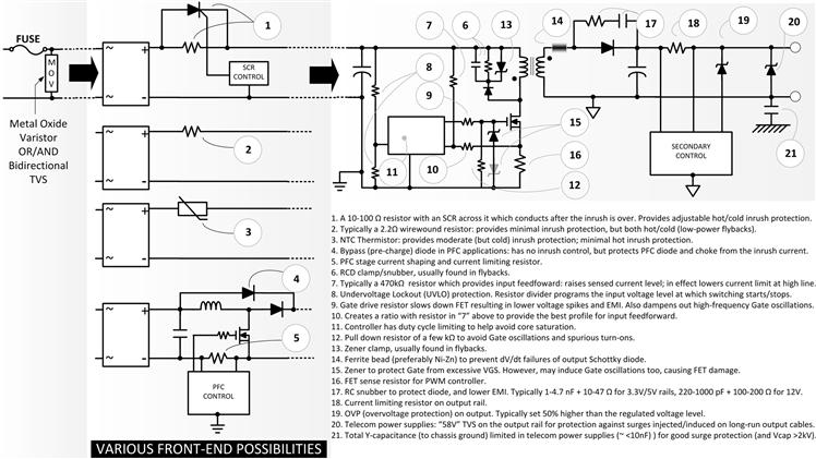
Figure 6.1: Various circuit-level protections for reducing stresses and enhancing reliability in AC–DC power supplies.
Recognizing the different equipments and operating environments, there is a new emerging standard for “PCDs” (power conversion devices) called IPC-9592 (available from www.ipc.org). This classifies power supplies as
Class I: General purpose devices operating in controlled environments, with intermittent and interruptible service, with an intended life of 5 years. Examples are power supplies in consumer products.
Class II: Enhanced or dedicated service power supplies in controlled environments, with limited excursion into uncontrolled environments, having uninterrupted service, and a life expectation of 5–15 years (typical 10 years). Examples are power supplies in carrier-grade telecom equipment and network-grade computers, medical equipment, and so on.
Incidentally, IPC-9592 also carries easy-lookup derating charts both for Class I (or “5-year”) Stress Factors and Class II (or “10-year”) Stress Factors. Expectedly, the latter occasionally provides more headroom through lower Stress Factors. However, as indicated several times, derating charts are best treated as guidelines, not rules — especially in power supplies where matters vary widely over topologies, applications, requirements, operating conditions and so on.
Component Ratings and Stress Factors in Power Supplies
Having understood overall systems-level stresses, we now look at the key power components used in power supplies and discuss those particular ratings and characteristics of theirs that are relevant to their proper selection in the particular application. We will see that there are many concerns connecting cost, ratings, application, performance, and reliability, often conflicting, that we need to weigh in any good power supply design — it is not just all about derating. We will observe that eventually there are no hard-and-fast rules, just guidelines, and above all: power supply design expertise combining common-sense and experience.
Diodes
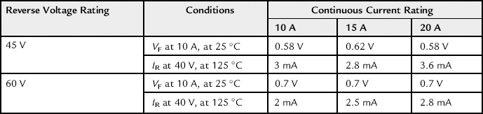
As an example, take the “MBR1045” diode, a popular choice for either 3.3 V or 5 V outputs of low-power universal input AC–DC flyback power supplies. Its datasheet is readily available on the web. This diode is, by popular numbering convention, a “10 A/45 V” Schottky barrier diode.
(a) Continuous Current Rating: The MBR1045 has a continuous average forward current rating (IF(AV)) of 10 A. We note that in a power supply, the average (catch) diode current is equal to the load current IO for both the Boost and the Buck-Boost/flyback topologies, and is equal to IO×(1 – D) for the Buck/forward topologies (in CCM). Note that in the latter case, the average current is at its highest as D approaches 1, that is, as the input voltage falls. That is a rudimentary example of the “Stress Spider” we will talk about in Chapter 7. So finally, as an example, if we pass 8 A average current through the MBR1045, its continuous current Stress Factor is 8 A/10 A→80%. That is acceptable from the point of view of current stress derating. However, in practice, we rarely operate a diode with that high a current. To understand why that is so, we need to understand the current rating a little better.
IF(AV) as specified in its datasheet is by and large a thermal limit. Typically, it is the current at which TJ (the junction temperature) is at its typical maximum of 150°C. Note that we can come across diodes rated for a max TJ (TJMAX) of 100°C (very rare), 125°C, 150°C (most common), 175°C, or even 200°C (an example of the latter being the popular glass diode 1N4148/1N4448). For smaller diodes (axial or SMD), intended for direct mounting on a board, the continuous current rating is specified with the diode assumed to be virtually free-standing, exposed to natural convection, or specified as being mounted on standard FR-4 board with a specified lead length, if applicable. The current rating falls as the ambient exceeds 25°C, to prevent TJ from exceeding TJMAX. For larger packages like the TO-220 (e.g., MBR1045), the continuous rating is specified with an “infinite (reference) heatsink” attached to the metallic tab/case of the diode. So, as per the datasheet of the MBR1045, we can pass 10 A up to around 135°C ambient. But that is only with an infinite heatsink (e.g., a water-cooled one). Much less current can be safely passed in a real-world situation with a real-world heatsink. We ask: what is the real-world maximum current rating of the diode? Unfortunately, that is for us to calculate as per the vendor — based on the characterization data made available to us by the vendor (the internal Rth and the forward voltage drop curves) combined with our estimate of the thermal resistance of the heatsink we are planning on using. The key limiting factor in all cases is the specified max junction temperature. It is our responsibility to ensure we do not exceed that value (with some safety margin too if desired).
Note that as per its datasheet, above 135°C ambient, the continuous rating of the MBR1045 is steadily reduced with rising ambient temperature. The reason for that is when we pass 10 A continuous current through this diode, we get an estimated 15°C internal temperature rise (from junction to case). So, with the infinite heatsink, and case held firmly at 135°C, the junction temperature is at 150°C. Therefore, above 135°C ambient, we need to steadily lower the current rating of the diode to avoid exceeding the maximum specified junction temperature. We ask: what is the max continuous rating at an ambient of 150°C? The answer is obviously zero, since we cannot afford the slightest additional heating when TJ=TJMAX. That is how we get the almost linear sloping part of the current rating curve extending from 135°C to 150°C as per the datasheet of the part.
Note that this steady reduction of current rating with respect to temperature is sometimes, somewhat confusingly, referred to as a “derating curve.” Resistors too, come with a similar published power derating curve (usually above 70°C), and for much the same reason. But we should not get confused — the use of the word derating in this particular case refers strictly to a reduction in the strength (i.e., the rating) of the part, not to any relationship between the strength and the applied stress.
For arguments sake, we can ask: why can we not pass more than 10 A below 135°C for the MBR1045, albeit with an infinite heatsink? In other words, why is the derating curve “capped” at 10 A? We argue: since the junction is at 150°C with the heatsink held at 135°C, if we lower the heatsink temperature to say 125°C, wouldn’t the junction temperature fall to 140°C? And so, wouldn’t that in turn allow for a higher current, so we can bring the junction back to its max allowed value of 150°C? The reasons for the 10 A hard limit include long-term degradation/reliability concerns and also “package limitations.” For example, the bond wires (connecting the die to the pins) are limited to a certain permissible current too. That rule of thumb is
![]()
This can also be written more conveniently in terms of mils as
![]()
Note that the above bond-wire equations apply to the more common case of copper or gold bond wires with length exceeding 1 mm (40 mil). For shorter bond wires, “A” can be increased to 30,000 (“B”=0.95). For aluminum wires exceeding 1 mm, “A” is 15,200 (“B”=0.48). For wires less than 1 mm, “A” is 22,000 (“B”=0.7).
Returning to the typical recommended current Stress Factor for catch diodes, in a power supply design the current-related Stress Factor is set closer to 50%, that is, 5 A in the case of the MBR1045, if not lower. The reason for that is very practical: the forward voltage drop of the diode (called VF or VD) is much higher when operated close to its max rating, and therefore the resulting dissipation (VF×IAVG) and the corresponding thermal stress can become significant. The efficiency gets adversely affected too.
(b) Reverse Current: Thermal issues always need to be viewed in their entirety — in particular in the context of system requirements (e.g., an efficiency target) and component characteristics, not to mention topology/application-related factors. For example, the reverse (leakage) current of Schottky diodes climbs steeply with temperature. The leakage also varies dramatically from vendor to vendor and we should always double-check what it is, compared to what we assume it is. The reverse leakage term is a major contributor to the estimated dissipation and the actual junction temperature of any Schottky diode in a switching application. After all, with 45 V reverse voltage and with just 10 mA leakage, the dissipation with D=0.5, is 45×10×0.5=255 mW. To reduce this term we want to reduce the diode temperature by better heatsinking.
In general, thermal runaway can occur with small heatsinks (or no heatsinks). The reason is an increase in temperature can cause more dissipation, leading to more dissipation and heating, and higher temperatures, in turn leading to higher dissipation, and so on. However, the forward voltage drop of the Schottky improves (reduces) at high temperatures (for a given current). It is a “negative temperature coefficient” device (for the range of currents it is intended for). For that reason we actually want it to run it somewhat hot. But its reverse leakage current can increase dramatically with temperature, leading to thermal runway for that reason. We have to strike a good compromise on temperature here.
Note the importance of application too. For example, if the Schottky diode is being used only in an OR-ing configuration (as in paralleled power supplies discussed in Chapter 13), its reverse current is clearly not an issue and we can increase the temperature-related Stress Factor closer to that of ultrafast diodes. In ultrafast diodes, reverse leakage is negligible, but its forward drop similarly decreases with temperature.
The forward voltage drop of both Schottky and standard ultrafast diodes can, in principle, increase with temperature, but that happens at very large currents, usually well beyond the continuous rating of the device. So, for all practical purposes both ultrafast diodes and regular Schottky diodes are negative temperature coefficient devices and we want to run them hot to improve efficiency. But as mentioned, the reverse leakage for Schottky diodes can become an issue. So we don’t want to run a Schottky “that hot.”
In Power Factor Correction (PFC) applications the silicon carbide (SiC) diode, discussed in Chapter 14, is becoming increasingly popular as the Boost/output diode since it has very fast recovery (~15 ns) and therefore prevents significant efficiency loss from occurring due to the reverse current spike when the PFC switch turns ON. The SiC diode is essentially a Schottky barrier diode, but a “wide bandgap device” offering very high reverse voltage ratings (up to several kV). It has about 40 times lower reverse leakage current than standard Schottky diodes (and unfortunately a higher forward voltage drop too). Note that unlike regular Schottky diodes, it is a positive temperature coefficient device, which means its forward voltage increases with temperature (above a certain current that is usually well within its upper operating range). So, we do want to run this diode cool if possible, to improve efficiency. The reverse leakage current of both SiC and ultrafast diodes is not significant.
Taking everything into account, we can target a conservative junction temperature of about 90°C for standard Schottky diodes (on account of negative temperature coefficient but high leakage current), 105°C as the junction temperature of SiC diodes (on account of positive temperature coefficient and low leakage), and 135°C for ultrafast diodes (on account of negative temperature coefficient and low leakage). That gives us a temperature derating factor of 90/150=0.6 for Schottky diodes, 105/150=0.7 for SiC diodes, and 135/150=0.9 for ultrafast diodes. Here, we are assuming all the diodes we are talking about are meant for switching applications (e.g., as catch diodes), and also that all have a TJ_MAX=150°C. If TJ_MAX is lower, or higher, than 150°C we can adjust the target junction temperatures based on the above-mentioned Stress Factors.
(c) Surge/Pulsed Current Rating: Diodes also have a surge current rating called IFSM or ISURGE. This is the maximum (safe) momentary current. We can visualize that a surge will not produce a steady buildup of temperature, but can cause sudden localized heat buildup inside the diode. There would be no time for any external heatsink, infinite or not, to react. It would not even depend on the bond-wire thickness. The hot-spot temperature inside the silicon junction is usually allowed to go up to around 220°C, since above that threshold the typical molding compounds of the surrounding package suffer decomposition/degradation. The MBR1045 for example, has a very high single-pulse surge current rating of 150 A. In a repetitive pulse scenario, we have to combine the localized heat buildup from every pulse with a dissipation term based on the ratio of the energy dissipation pulse width to the period of repetition. The pulsed surge rating thus comes down as the repetition rate increases. Eventually, it equals the continuous current rating.
But does the surge rating of diodes really matter to us in switching power supplies? In fact it does not, not when we are selecting the output/catch diode. In that location, the inductor serves to limit the current in both the diode and the FET. After all, the diode only takes up what is an almost constant current source (the inductor current) during the off-time, and the FET takes up the same during the on-time. However, the surge rating of diodes is a major concern in the design of the front-end of AC–DC power supplies, because that is the place where we normally connect a voltage source almost directly across a capacitor, leading to an almost unrestricted momentary current through the diode and into the capacitor as charging current as discussed in Chapter 1. In particular, we need to consider the surge rating of diodes in two front-end cases: (a) when we select the bridge rectifiers for AC–DC power supplies, those without Power Factor Correction (PFC), and (b) when we select the pre-charge diode often found in well-designed commercial front-end Boost-PFC stages (see Figure 6.1, bullet 4). In the former case, to save the diodes, we also need to include inrush protection, either active (usually with an SCR), or passive (with an NTC varistor, but sometimes with just a 2 Ω wirewound resistor in series). In PFC stages, the pre-charge (bypass) diode can be found strapped directly across the PFC inductor and the Boost/output diode (see Chapter 14). Its purpose is to divert the inrush/surge current flowing into the PFC Boost output capacitor when we first connect the AC mains. That huge current then goes through this appropriately rated diode rather than possibly damaging the inductor and/or Boost diode on the way. An example of a diode explicitly intended for this bypass function is the 10ETS08S, available from several vendors. It is a 10 A/800 V standard recovery (slow) diode, with a huge 200 A non-repetitive surge rating. It also has published “I2t” and “I2√t” (fuse current) ratings. On the other hand, its forward drop or continuous current ratings really do not matter, since this bypass diode eventually suffers the “ignominy of getting bypassed” itself — it automatically stops conducting the moment the PFC stage starts switching. Note that the front-end of power supplies along with PFC is discussed in further detail in Chapter 14.
(d) Reverse Voltage Rating: Coming to voltage, the MBR1045 has a maximum reverse repetitive voltage (VRRM) rating of 45 V. In general, we want to keep within that rating, preferably with a Stress Factor of less than 80%. That includes any spikes and ringing of a repetitive nature. To dampen those spikes out, we may need to put in a small RC (or just a C) snubber across the diode (see Figure 6.1, bullet 17). Snubbers also greatly help in reducing EMI, though they can add significantly to the dissipation of the diode, especially if only a C-snubber is used instead of an RC-type (the C-snubber dumps most of its stored energy per cycle into the diode, instead of dumping it into the R of the RC-snubber). Note that we can often tweak the turns ratio n=NP/NS of the transformer in flyback applications (within reason) to accommodate the diode’s reverse rating. Increasing the turns ratio produces a lower reflected input voltage across the Secondary.
Though we prefer to target an 80% Stress Factor for the reverse voltage, we may have to make a strategic call in some designs and allow that margin to get a little worse. Because, if for example, in an effort to improve the safety margin we pick a 10 A/60 V diode instead of a 10 A/45 V diode, the efficiency may get degraded. Because, generally speaking, for a given current rating, a diode with a higher voltage rating has a higher forward voltage drop at a given current. Though one way out to increase both the safety margin and keep the forward drop low, is to consider a higher current 60 V device, like a 15 A or 20 A diode instead of the MBR1045 or a 10 A/60 V diode, cost permitting. Because, generally speaking, for a given voltage rating, a diode with a higher current rating has a lower forward voltage drop at a given current (though this is a trend; it may not be really true as we can see from Table 6.1). Unfortunately, a diode with higher current rating also has a higher reverse leakage current than a diode with lower current rating of the same voltage rating. Quite the contrary, a diode with a higher voltage rating has a lower reverse leakage current than a diode with a lower voltage rating of the same current rating.
A higher leakage current will lead to a higher dissipation in switching applications irrespective of the forward loss. See Table 6.1 for actual data extracted from one particular vendor. However, take nothing for granted, especially for reverse leakage. For example, the 3 mA reverse leakage of the MBR1045 from Fairchild compares very favorably to the 10 mA stated for the MBR1045 from On-Semi (under the same conditions), and the 100 mA for the “equivalent” SBR1045 from Diodes Inc. However, the MBR1060 from Fairchild has an IR of 2 mA, and that is outclassed by the 0.7 mA of the MBR1060 from On-Semi.
If we are very keen to lower the forward voltage drop, we might like considering paralleling lower current diodes. For example if we take two MBR745 diodes from Fairchild and ask them to share the 10 A current equally (5 A in each), we see from the corresponding datasheet from Fairchild that the forward drop of the MBRP745 is only 0.5 V at 5 A and at 25°C. That is an improvement over the almost 0.6 V from a single 10 A/45 device. However, each MBRP745 has a leakage of 10 mA at 40 V and at 125°C, so two diodes in parallel will give us a whopping 20 mA reverse leakage. Further, to get two diodes to share properly is not trivial. One way to force that is by paralleling two diodes on the same die (dual pack). Another way is shown in the context of EMI suppression in Figure 17.4.
In brief, power supply design is all about trade-offs — very careful trade-offs as exemplified in this “simple case.”
There is a possible way of allowing for a voltage Stress Factor equal to or exceeding 1 and yet not compromising reliability. We know that Schottky diodes typically “avalanche” (behave as zeners) if the reverse voltage exceeds about 30–40% of their VRRM. That property can be used to deliberately clip any spikes without using snubbers or clamps. But regular Schottky diodes can handle this zener mode of operation for a very short time only. For reliable operation, the Schottky diode must have a guaranteed avalanche energy rating (EA expressed in μJ) stated in its datasheet, and we have to confirm from our side that the energy of the spike that it is being used to clamp in our application is well within that particular rating. An example of such a “rugged” diode is the STPS16H100CT from ST Microelectronics. This is a dual common-cathode diode package, with each diode being rated 8 A/100 V. Diodes Inc. calls such a diode a Super Barrier Rectifier (SBR®). For example, they offer a 10 A/300 V rectifier called the SBR10U300CT.
(e) dV/dt Rating: We all know that a diode has peak/surge/average current ratings. It also has a well-known steady reverse (blocking) voltage rating. But whereas voltage is certainly a known stress, its rate of rise (or fall), dV/dt, can also produce overstress and corresponding failure modes. ESD, as discussed above, is in effect a dV/dt stress. It is well-known that MOSFETs are vulnerable to ESD, especially during handling, testing, and production. Another example is the Schottky diode. The Schottky has a maximum rated dV/dt, usually specified somewhere deep in its datasheet that engineers often miss. What could happen is that in a real application, we may have applied what we believe is a “safe” steady reverse DC voltage within the Abs Max reverse voltage rating of the diode, yet we learn that some diodes are failing “mysteriously” in large-scale production testing. One reason for that could be a momentary amount of excess dV/dt every switching cycle that we can capture only on an oscilloscope if we zoom in very carefully. The likelihood for this type of violation is naturally the highest when the diode is in the process of getting reverse-biased (switch turning ON). Even a little ringing in the turn-off voltage waveform for example, usually due to poor layout, can cause the instantaneous dV/dt at some point of the waveform to exceed its dV/dt max rating, causing damage. Nowadays, the dV/dt rating of Schottky diodes has almost universally improved to 10,000 V/μs and that has greatly helped forgive the lack of attention to this very rating. But not very long ago, diodes with 2,000 V/μs or less were being sold as “equivalents,” purely based on the fact that their voltage and current ratings were the same as more expensive competitors. Perhaps we still need to be watchful for that possibility today. If necessary, we may need to slow down, dampen, or smoothen out the turn-off transition somewhat. We can do that by trying to slow down the switching transition by increasing the Gate resistor of the FET (though admittedly, that usually just creates more delay till the turn-off transition starts, rather than slowing the transition itself). An effective “trick” used in commercial flybacks is to insert a tiny ferrite bead in series with the output diode (see Figure 6.1, bullet 14). This can certainly adversely impact overall efficiency by a couple of percentage points, but it can raise the overall reliability significantly. Note that Ni–Zn ferrite offers higher high-frequency resistance and lower inductance than the more common Mn–Zn ferrite. So, a Ni–Zn bead affects the energy transfer (flyback) process less (as we want), but is much better at providing (resistive) damping against any high-frequency ringing that can be responsible for dV/dt violations during the diode turn-off transition.
Table 6.1. Schottky Diode Forward Voltage Drops and Reverse Leakage Currents.
Datasheets Consulted: MBR1045, MBR1060, MBR1545CT, MBR1560CT, MBR2045CT, and MBR2060CT, all from Fairchild Semiconductor. Typical values extracted from curves.
MOSFETs
For example, let’s take the “4N60” N-channel MOSFET (also called a “FET” here). This (or an equivalent) is a possible choice for low-cost universal input AC–DC flybacks up to around 50 W. By popular numbering convention the 4N60 is a 4 A/600 V MOSFET.
(a) Continuous Current Rating: Like diodes, FETs also have continuous/pulsed current and sometimes avalanche ratings too (“rugged” FETs). The continuous rating is once again, in effect, just a thermal limit. For the 4N60 in a TO-220 package, that rating is 4 A when mounted on an infinite heatsink at 25°C. But with the case/heatsink at 100°C, the rating is only 2.5 A (typical; depending on the vendor). Because under that condition the junction is already at 150°C.
The RDS is also always stated with the case held at 25°C, passing what may often seem quite an arbitrary current through the device. The real calculations can be very tricky and iterative, because the RDS of a FET depends strongly on junction temperature (and on Drain current too). But we can also take the approach of believing the data provided by a reliable vendor to reverse-estimate the RDS. For example, take the 4 A/60 V TO-220 device (STP4NK60Z) from ST Microelectronics. The stated junction-to-case thermal resistance of this device is 1.78°C/W. The vendor also states that with the case held at 100°C, the maximum Drain current is only 2.5 A. We can assume that under this condition, the junction is already at 150°C. So, the temperature rise from case to junction is 150−100=50°C. Our estimate of worst-case RDS (at a junction temperature of 150°C) is therefore
![]()
Note that the RDS stated in the datasheet is “2Ω” under rather benevolent conditions of case held at 25°C and the device passing only 2 A current. We see that in reality, the worst-case RDS is 2.25 times more. That is actually a typical “cold to hot RDS factor” when dealing with high-voltage FETs for AC–DC power supplies. For logic-level FETs (say 30 V and below), the hot to cold RDS factor is only about 1.4.
The 4N60 is also available in SMD packages (e.g., TO-252/DPAK, or the TO-263/D2PAK, the latter being basically a TO-220 laid down flat on the PCB). Since these do not involve an infinite heatsink, the continuous current rating is much lower. The common feature between the two 4N60s in different packages is just their RDS. And in all cases, for all packages and any heatsinking, the max continuous rating is based on the junction temperature being at a maximum of 150°C.
Note that whereas in diodes, it was relatively easy to estimate TJ and thereby estimate the thermal stress, in the case of a FET it is much harder to do. Even if we do know the RDS accurately, what we can calculate so far is just the conduction loss term. To estimate the actual junction temperature in a switching application, we have to also carefully add switching losses as discussed in Chapter 8.
The 6N60 (or equivalent) is often used in universal input flyback power supplies up to 70 W. It is rated 6 A/600 V. Its RDS is 1.2 Ω (typical 1 Ω). With an infinite heatsink held at 100°C, its continuous current rating drops to 3.5 A to 3.8 A (depending on the vendor). As was the case for a diode, there are efficiency concerns that prevent us from approaching anywhere close to the continuous current rating of a FET. For example, in 70 W flybacks, the measured peak switch current may be only between 1.5 A and 2 A worst-case under steady conditions (measured with max load at 90VAC). The average switch current, assuming D=0.5, is therefore 0.75 to 1 A. Nevertheless, the 6N60 is used for this application. The current-related Stress Factor is 1 A/3.8 A=0.26, or about 25%. Therefore, we can see that significant continuous current derating has been applied in the interests of power supply efficiency. Flyback power supply designers therefore may declare as a rule of thumb that they use “a FET with a hot-RDS of 2 Ω for 2 A peak, 4 Ω for 1 A peak, 1 Ω for 4 A peak ….” and so on.
Power supply designers sometimes forget that the applied Gate-to-Source voltage (VGS) can also affect the RDS. The stated RDS of 2.5 Ω for the 4N60 or 1.2 Ω for the 6N60 is with VGS=10 V. These FETs typically have a Gate threshold voltage of around 4 V. As power supply designers, we must in general try to ensure that the ON-pulse applied to the Gate has an amplitude greater than about 2× the Gate threshold voltage of the part. Otherwise, the RDS will be higher than we had assumed.
Note: To estimate temperature and/or conduction loss, it is important to ultimately measure the RDS carefully in our switching application — by calculating the ratio of the measured Drain-to-Source voltage VDS when the switch is ON (its forward drop) to the corresponding measured Drain current ID. Neither of these are trivial measurements. ID is best measured by snapping in a current probe on a loop of wire connected to the Drain of the FET. Remember: we should never put a current probe on the Source of a FET because even the small inductance of the wire loop can cause ringing and spurious turn-on, leading to FET damage. For a VDS measurement we may think it is OK to place the typical 10×voltage probe of a scope from Drain to Source while the FET is switching and zoom in to see the small voltage drop across it during the ON-time. Unfortunately, a typical scope has a vertical amplifier that will “rail” and saturate by the hundreds of volts of off-screen high voltage during the OFF-time. So the ON-time measurement will in turn be absurd, because the vertical amplifier is still trying to recover from the effects of overdrive. Therefore, the engineer may need to devise a small, innovative and non-invasive buffer circuit (i.e., a circuit with high enough impedance and minimum offset so as not to affect either the current through the FET or its observed forward voltage drop), and then place this little circuit on the Drain. The output of this buffer circuit is intended to be a true reflection of the VDS during the ON-time, but clamped to a maximum of about 10–15 V during the OFF-time. The voltage probe of the scope is placed on this output node, rather than directly on the Drain of the FET to avoid saturating the scope amplifier.
Another technique that can help avoid overdrive of the scope amplifier is to use waveform averaging on the scope, then use the scope’s waveform math functions to digitally magnify the waveform around the portions of the signal of interest. Digital magnification performs a software expansion of the captured waveform to reveal additional vertical resolution beyond the typical 8-bit resolution of the scope’s ADC (when averaging is used).
(b) Surge/Pulsed Current Rating: As in the case of a diode, the inductor limits the current, so the surge rating of a FET is not really tested out in switching power supplies. But the rating can matter in poorly designed power supplies. For example, as mentioned previously, flybacks are prone to damage at initial power-up or power-down. The reason for that is for this topology, the center of the current ramp (of the inductor/switch/diode) is IOR/(1 – D) as explained in Chapter 3. So, as the input voltage is lowered, D approaches 1 and the sudden rise in current can cause core saturation, which in turn can cause a huge current spike in the FET, damaging it. A common technique to guard against power-up and power-down damage at low line in flybacks is by incorporating careful current limiting, combined with UVLO (under voltage lockout) and maximum duty cycle limiting (see Figure 6.1 once again).
At high-line, sudden overloads can cause a huge current spike at turn-off, that can lead to a voltage spike across the FET, killing it. A technique to guard against that is “Line (or Input) Feedforward.” This is also discussed in Chapter 7. In general, without adequate protection against these “low-frequency repetitive events,” no amount of steady-state stress derating will be sufficient to ensure field reliability.
(c) Drain–Source Voltage Rating: In a commercial flyback using cost-effective 600 V FETs, the conservative expectation of 80% voltage Stress Factor, or 0.8×600=480 V is not feasible. In well-designed commercial power supplies (with all the protections mentioned above and as indicated in Figure 6.1 included), the voltage Stress Factor for power MOSFETs is often set closer to 90% — because now, very few situations are considered anomalous or unanticipated. For the 4N60 or the 6N60 in flyback applications, that is a maximum of 0.9×600=540 V including spikes — measured at 270VAC under steady conditions while sweeping all the way from min to max load to confirm the worst-case. The desired minimum headroom is 60 V.
(d) Gate–Source Voltage Rating: MOSFETs are very easily damaged by voltages (even extremely narrow spikes) that are in excess of the specified Gate-to-Source Abs Max voltage. The Gate oxide can be easily punctured, even by electrostatic charge picked up by walking across a carpet for example. Once mounted on a board, the potential for ESD damage is obviously minimized. The 4N60 and 6N60 are both rated for ±30 V maximum VGS. For this reason we may sometimes find protective zeners connected from Gate to Primary Ground of the switching FET in power supplies. Note that, as indicated in Figure 6.1, because of the high impedance of the Gate, very high-frequency oscillations are possible between the trace inductance running to the Gate and the input capacitance of the FET (at the Gate pin). There is also anecdotal evidence to suggest that “protective” zeners placed at the Gate terminal can exacerbate such oscillations and lead to “mysterious” field failures. It is therefore always recommended to put in a Gate drive resistor to dampen out any potential oscillations as shown in Figure 6.1. A 4.7–22 Ω resistor is standard. A pull-down resistor of a few kΩ placed very close to the Gate is also recommended to avoid oscillations and spurious turn-ons, especially in AC–DC switching power supplies.
(e) dV/dt Rating: In the early days of MOSFET, the most common failure mode was due to very high “reapplied dV/dt.” This could trigger the parasitic BJT (bipolar junction transistor) structure inside the MOSFET and lead to avalanche breakdown and snapback. It can occur even today, but it is very rare, so we virtually ignore this possibility nowadays. Modern FETs can handle 5–25 V/ns (i.e., over 5,000 V/μs).
Capacitors
In general, we have to be conscious of the voltage rating of any capacitor and stay under that limit and preferably with some typical derating. Polarized capacitors like aluminum electrolytic and solid tantalum also have reverse voltage ratings that we must not exceed, though aluminum caps are more tolerant than solid tantalum in this regard.
In general, in the interest of cost, we should confirm with the capacitor vendor whether their specific test/field data really support the traditional notion that voltage stress derating is useful in lowering the field failure rate of capacitors. That relationship seems to be in question today given the improvements in manufacturing technology. This is especially true for aluminum electrolytic caps. We can explain that specific situation as follows. The breakdown voltage of an electrolytic cap is not an abrupt threshold. It is related to the thickness of a chemically generated oxide on its electrodes. That oxide film is the dielectric that holds-off the applied voltage. If the working voltage on the cap is increased, the oxide thickness also gradually increases, raising the voltage withstand capability. On the other hand, if the working voltage is reduced, the oxide can also reduce gradually, lowering the rating (though the addition of borax greatly prevents that). That is the reason why if we take aluminum electrolytic caps out of storage after a long time, a “re-forming” phase is still recommended by many vendors, in which the applied DC voltage is slowly ramped up (with max current limited to a few mA), to let the oxide develop fully again. But this also indicates that if we operate an aluminum electrolytic cap at reduced voltages for a long period of time, its “strength” progressively lowers, and so the presumed safety margin also falls somewhat over time.
All capacitors usually have a published ripple current rating that we must not exceed. The most important parameter for aluminum electrolytic capacitors in particular, is its life, which is based on its “core temperature,” which in turn depends on the RMS current passing through it in a given application. The max RMS (ripple) current rating is therefore a thermal rating in effect. For extending life, we may need to apply a derating to the ripple current rating. Life prediction is discussed later in this chapter.
Film capacitors are prone to dV/dt failures. The common, low-cost Mylar® (polyester/KT/MKT) capacitors are rated for only about 10–70 V/μs. They are therefore usually not suitable for snubbers or clamps. For AC–DC flyback snubber/clamp applications, a preferred film capacitor type is polypropylene (KP/MKP), since its dV/dt rating is typically 300–1,100 V/μs. The ceramic capacitor and the mica capacitor both have very high dV/dt ratings, and for cost reasons, the former is often used for clamps today. Note that film capacitors are generally favored in many situations over ceramic, since they are far more stable (less change in capacitance and other characteristics) with respect to applied voltage, temperature, and so on.
Keep in mind that both the dV/dt and dI/dt ratings of any selected capacitor can get fully tested at the front end of both AC–DC converters and DC–DC converters. We need especially high transient ratings for that particular location. This is further discussed in Chapter 14.
In solid tantalum (Ta-MnO2) capacitors in particular, a high dV/dt can produce a large surge current due to I=C(dV/dt). This can cause localized heating and immediate damage. For that reason it is often said that most tantalum capacitors rated for say “35 V,” should not be used at operating voltages exceeding half the rated voltage (in this case 17.5 V). That is especially true at the front-end of any power supply (DC–DC converter) where even that amount of derating may not be enough. We actually need to limit the surge current to avoid local defects from forming in the oxide and mushrooming into failure. It is often recommended to ensure at least 1 Ω per applied Volt in the form of source impedance to limit the surge current to a maximum of 1 A. Conservative derating practices call for 3 Ω/V, which will limit the current to 333 mA. Still more conservative engineers do not even use Ta-MnO2 capacitors anymore, and prefer ceramic or polymer caps.
Modern multilayer polymer (MLP) capacitors are stable, have very high dI/dt and dV/dt capabilities, and are being increasingly preferred in many applications to multilayer ceramic capacitors (MLCs), Ta-MnO2 capacitors, and aluminum electrolytics. They are available up to 500 V rating and offer very low ESR for power converter output applications.
Ceramic capacitors at the front-end of a converter can themselves induce a huge voltage spike when power is first applied on the input terminals of a converter. This “input instability” phenomenon is discussed in more detail in Chapter 17. One solution is to place an aluminum electrolytic capacitor in parallel to the input ceramic capacitor, as a means of damping out the input oscillations.
An aluminum electrolytic capacitor, besides its well-known advantages of delivering maximum “bang for the Buck” (very high capacitance times voltage for a given volume plus cost) is extremely robust too. Its failure modes are essentially thermal in nature. So, it can withstand significant abuse for short periods of time. For example, we can typically exceed an aluminum capacitor’s voltage rating by 10% for up to 30 seconds with no impact. That is called its “Surge Voltage rating.” It also has an almost undefined surge current rating. It can, for example, tolerate extremely high inrush currents at the input of an AC–DC power supply with no problem at all, provided the inrush is not made to occur repetitively and too rapidly. The aluminum electrolytic has self-healing properties since its oxide layer quickly reforms. It rarely ever fails open or short unless thoroughly abused (in which case it vents). Its normal failure mode is essentially parametric in nature (e.g., drift of capacitance, ESR, and so on). Its Stress Factors therefore may not be of such great concern as concerns about its lifetime, as discussed later in this chapter.
PCB
A major power component frequently overlooked is the PCB itself. In power supplies this is also subject to power cycling and resulting hot-spots that we must guard against. If we open a commercial power supply, we may find power resistors mounted on raised standoffs rather than flush against the PCB surface. That is to protect the PCB from overheating. Standard FR-4 PCB material has a glass transition temperature TG of around 130°C and is therefore rated for 115°C maximum. If we cross the glass transition threshold, the properties of the board can change in a subtle way, often permanently. For one, the TCE (Thermal Coefficient of Expansion) of the board can get affected and that can lead to subtle failures down the road, as explained a little later below.
In general, just as dV/dt can cause overstress, a high rate of change of current, dI/dt, can also cause failures. For example, we know that V=L dI/dt. So if nothing else, a high dI/dt on a PCB trace can cause a voltage spike that can indirectly kill a semiconductor. It is known that very fast diodes with extremely snappy recovery characteristics can produce very large voltage spikes due to their abrupt current cutoff (which is in effect a large dI/dt). This voltage spike can then damage the very diode that has indirectly created it, or can even damage any weaker component in its neighborhood. Bad PCB layout can also cause similar inductive spikes, large enough to cause failures. See Chapter 10 for more details.
Mechanical Stresses
Lastly, while focusing on electrical stresses, we must not forget the seemingly obvious: mechanical stresses. We could cause damage, immediate or incipient, due to mishandling, drops, or transportation. For that reason a typical commercial power supply PCB will have generous dabs of RTV (room temperature vulcanizing silicone) on its PCB, literally anchoring down bigger components. Every commercial power supply needs to pass a shock and vibration test during validation testing. In this context, two- or multilayer PCBs fare much better than single-sided PCBs. Because large through-hole components mounted with their pins inserted through plated-through holes (vias) and soldered through the via onto the other side of the board, get anchored much better than single-sided PCBs where the traces can rip off rather easily.
However, there are more subtle forms of failure due to mechanical stresses. In power supplies, as power and temperatures cycle up and down, significant expansions and contractions occur constantly. Generally, the “thermal coefficient of expansion” (called TCE or CTE) of SMD components differs from the TCE of the PCB on which they are mounted. So, relative movement occurs that can lead to severe mechanical stresses and eventual cracking. Surface-mounted multilayer ceramic capacitors, in particular, were historically extremely prone to this. Bad soldering practices can also initiate micro-cracks that develop into failures over time. Also note that large PCBs sag, much more than smaller PCBs, and that too produces severe stresses, especially on the relatively brittle SMD ceramic capacitors. Therefore, even today, though great efforts have been made to match the TCE of components to the TCE of standard FR-4 PCB material, many quality power supply design cum manufacturing houses still have strict internal guidelines in place restricting their power designers from using any SMD multilayer ceramic capacitor larger than size-1812 (0.18 in.×0.12 in.), for example, even size-1210 on occasion.
“Lead forming” or “lead bending” has been used for decades in power semiconductors. One motivation for that is convenience. For example, the device may be mounted on a heatsink in such a way that to be connected to the PCB, the leads really need to be bent. However, stress relief is also a motivation here. With a little bend introduced in the leads, we can prevent mechanical stress due to thermal cycling from being transmitted into the package causing damage in the long run. However, we have to be cautious that in the process of performing lead bending to avoid long-term stress, we do not cause immediate stresses and incipient damage. In plastic packages, the interface between the leads and the plastic is the point of maximum vulnerability. Under no circumstances must the plastic be held or constrained while the leads are bent, because the plastic–lead interface can get damaged. And when that happens, even though the damage is not obvious, the ability of the package to resist ingress of moisture is affected. That may eventually lead to device failure through internal corrosion.
Part 2: MTBF, Failure Rate, Warranty Costs, and Life
Having provided a background on basic reliability concerns in power supply design we move on to an overview of reliability/life prediction and testing.
MTBF
The first term we should know is power-on hours or “POH.” For components/devices, this may be called total device-hours (“TDH”) instead, but the concept is the same. For example, one unit operating for 105 (100k) hours has the same power-on hours as 10 units operating for 10k hours, or 100 units operating for 1,000 h and so on. All these give us 105 POH. (To be statistically significant however, a larger number of units is always preferred.) Note that whenever people talk of failure rate, or MTBF (Mean Time Between Failures), they usually talk in terms of “hours,” whereas in reality they mean POH or TDH. This should be kept in mind as we too undertake the specific discussion below.
Failure rate, λ, is the number of units failing in unit time. But it is expressed in so many ways and we need to know some inter-conversions. Historically, failure rate was first expressed as the % number of units/devices failing in 1,000 h of operation. Later as components with better quality emerged, people started talking in terms of the number of failures occurring in 106 (million) hours. That was called “ppm,” for parts per million. As quality improved further, the failure rate of components was more conveniently stated as the number of failures per billion (109) hours. That number is called “FITs” (failures in time), and is often referred to as λ too. See Figure 6.2 for an easy look-up table for failure rate conversions.
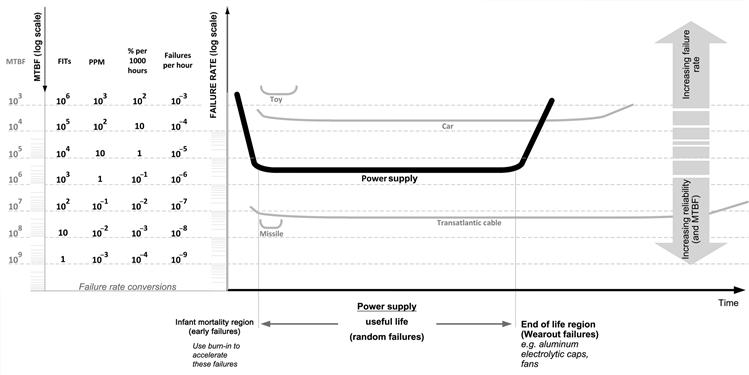
Figure 6.2: Failure rate conversions and the bathtub curve.
For example, a component with a failure rate of 100 FITs is equivalent to a ppm of 0.1. That incidentally is 0.1×10–6=10–7 failures/hour.
MTBF is the inverse of failure rate. Therefore, in our example here, for 100 FITs, the MTBF is 107 h (10 million hours). Similarly, an MTBF of 500k hours is equivalent to a failure rate of 0.2%/1,000 h, or a ppm of 2, or 2,000 FITs.
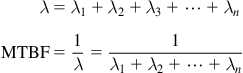
The failure rate of a system is the sum of the failure rates of its components (we are ignoring redundant systems here).
An MTBF of 250k hours is a typical expectation of certain types of power supplies. Since there are 8,760 h/year, 250k hours seems immense, close to 30 years. Does that mean we can take a very large sample of these power supplies and expect only one unit to fail on an average every 30 years? Not at all. The term MTBF is vastly misunderstood, and needs to be clarified.
An MTBF of 30 years actually means that after 30 years, provided there are no wearout failures (wearout is explained later), we will be left with a third of the power supplies that we started off with. In other words, two-thirds will fail by the end of the MTBF period (30 years in our case). So out of 1,000 units, about 700 units will fail. Out of 2,000 units, 1,400 units will fail, and so on. We can thus estimate how many hundreds will fail in 5 years.
By definition, MTBF is in fact the time constant of a naturally exponentially decreasing population.
![]()
Note that this is analogous to a capacitor discharging.
![]()
At the end of the time constant τ=RC, the cap voltage is 1/e=0.368 of the starting voltage.
The reliability R(t) is defined as
![]()
This is in effect the probability that a given piece of equipment will perform satisfactorily for time t because N(t) is the number of units left after time t and N the number we started off with. Note that reliability is a function of time. For t=MTBF, the reliability of any system/device is only 37%. Which is another way of saying that from the start, the equipment was only 37% likely to survive until t=MTBF. It has a lesser chance to survive longer and longer, which is why reliability falls exponentially as a function of time. Let us bullet out the different ways of stating MTBF and interpreting it:
(a) With a large sample, only 37% of the units will survive past the MTBF.
(b) For a single unit, the probability that it will survive up to t=MTBF is only 37%.
(c) A given unit will survive until t=MTBF with a 37% confidence level.
In our example, at the end of 5 years, we are left with
![]()
So 1,000–839=161 units have failed in the first 5 years. How about after 10 years? We are then left with only
![]()
So, 839–704=135 units failed between 5 and 10 years in the field.
Note: Here is the math that makes this an exponential curve: 161/1,000=135/839 (=0.161). We should know that the ratio by which an exponential curve changes in a certain time interval is invariant. In fact it does not matter where we set t=0. At any chosen starting point, N is the number of units existing at that moment. That is why the exponential is considered the most “natural” curve. On that basis we now expect that in the next 5 years (10 to 15 years) 0.161×704=113 additional units will fail, giving a total of 409 units failing in 15 years. There are two figures in this book that should be looked at more closely at this juncture to get a better idea of the exponential curve — Figure 5.3 and Figure 12.1. It will also become clear from the former figure in particular, why MTBF is perhaps an appropriate name for the time till the number of units falls to 1/e of the initial value. Because in a sense, based on area under the curve, on an average we can consider all the units as having failed at exactly this precise moment.
One last misconception needs to be cleared up: if the MTBF of a power supply goes from say 250k hours to 500k hours, does that mean “reliability has doubled”? No. First of all, the question itself is wrong. We need to specify “t” while calculating R(t). So suppose we pick t=44 k hours (5 years). This becomes the moment at which we are comparing reliabilities for the two MTBF possibilities (usually set to the expected life of the equipment). So,
![]()
We see that doubling the MTBF increased reliability by roughly only 10% over 5 years (because 92/84=1.095). But warranty costs do vary in inverse proportion to the MTBF.
Warranty Costs
Why is reliability so important in a commercial environment? Cost! Engineers should know the “10×rule of thumb” which goes as follows: if a failure is detected at the board level and costs $1 to fix, it will cost $10 if discovered at a system level (by a failure in production testing), and will cost $100 to fix in the field, and so on. Several subsequent studies actually show that the cost escalates far more rapidly than 10×. It therefore becomes very clear that if the power supply design engineer understands converter stresses and potential failure modes well in advance, and eliminates them at the design stage itself, that is the cheapest way to go.
Example:
If there are 1,000 units with an MTBF (Mean Time Between Failures) of 250k hours, how many units are expected to fail over 5 years? Calculate warranty costs, assuming it costs $100 to repair one unit.
In a real-world situation, damaged equipment will be immediately replaced and put back in the field. So, the average population in the field will not dwindle exponentially. In such a situation, we can calculate the recurring or annual warranty cost. Over the declared 5-year warranty period (43.8k hours), the number of failures is
![]()
That is 175.2/5=35 units per year for 1,000 units or 3.5 failures per 100 units. And that gives us the Annualized Failure Rate (AFR)
![]()
For our example, we have
![]()
Or 3.5 units failing every year for every hundred in the field. If it costs $100 to repair one unit, that gives us $350 per 100 units or $3.5 per unit every year for 5 years. The total repair cost over 5 years is an astonishing $17,520, or 17,520/5=$3,500 per annum — for 1,000 units sold, irrespective of the proposed selling price of each unit. In other words, the warranty repair cost per unit is $17.52 over the stated warranty period. This cost will need to be added to the selling price of the unit by the vendor upfront, or risk going bankrupt. An alternative is to reduce the warranty period, say to the bare minimum of 90 days.
Life Expectancy and Failure Criteria
In reality, the number of units failing will often climb steeply, typically at around the 5-year mark. That is because lifetime issues start to come into play at this point. Engineers should not confuse life with MTBF though both eventually lead to observed failures. The concept of MTBF applies only during the useful life of the equipment, during which, by definition, failure rate is a constant (implying an exponentially decreasing curve in the absence of any repairs and/or replacements). These are also called random failures. Ultimately, the failure rate suddenly climbs as a result of wearout (end-of-life) failures. See Figure 6.2 for the classic bathtub curve. We have tried to indicate how some systems have high reliability but low life (missile), whereas some have relatively low reliability but long life (car), and so on.
Though, what exactly is considered a failure also needs to be defined. The equipment need not become completely non-operational as a result of the failure; it may just fall out of specified performance limits. For example, a car may continue to function even though its seat belts or audio/GPS units are not working. It depends on us whether we deem that as a failure and pull the vehicle off the road for repairs. For any electronic component, what exactly those limits are, and what therefore constitutes the set of failure criteria, are specified in the electrical tables of its datasheet.
A key culprit for wearout failures of a system/equipment is the aluminum electrolytic capacitor, if present. We will discuss life prediction of this capacitor later in this chapter. Another common contributor to life limitations is the cooling fan, if present. Note that sleeve-bearing fans are commonly said to fare worse than ball-bearing ones in terms of life. However, ball-bearing fans also become noisier sooner, and if a certain threshold of noise is included as part of the failure criteria of fans, then sleeve-bearing fans are probably at par if not better than ball-bearing ones, and much cheaper too. Another component that can show steady degradation (wearout) is the optocoupler. If we apply a high anode current for an extended period of time, the current transfer ratio (CTR) of the opto can worsen steadily and quickly. The life on an optocoupler is said to be the point at which its CTR has fallen to 50% of its initial value. In general, overdriving a typical opto above ~10 mA causes a huge reduction in its lifetime. However, in a power supply application, we have a high-gain system, and so the slightest error-related current passing through the opto produces an immediate correction, which therefore reduces the current. So, we cannot really (continuously) overdrive the opto in a power supply feedback-loop application. We can therefore expect its life to be typically over 150k hours. Normally, we also have enough phase and gain margin built-in to prevent any instability due to CTR-related tolerances and degradation.
Component vendors often do “specmanship” around failure criteria or guaranteed performance limits. For example, Panasonic declares end-of-life for most of its leaded aluminum electrolytic capacitors on the basis of capacitance falling 20% below the initial value, but for its own SMD aluminum electrolytic, that number is 30%. Therefore, we need to compare failure criteria while comparing life or MTBF numbers provided by different vendors, but often even for different product families from the same vendor.
Reliability Prediction Methods
We would like to get an estimate of the prospective field reliability as early as possible. Till fairly recently, Military Handbook 217F (MIL-HDBK-217F) was widely used to predict reliability. It is no longer recommended today as it was consistently providing very pessimistic predictions based on an outdated database of component reliability figures, and was in effect obsolete. However, an effort is already underway to revise and re-invigorate it as the new VITA 51 standard (VITA stands for VMEbus International Trade Association) (see www.vita.com).
MIL-HDBK-217F went about reliability prediction in two ways — either using a simple Parts Count analysis, or a more detailed Part Stress analysis.
Parts Count was intended to be used only in initial project bidding phases when no prototype was available. It basically involved summing up the failure rates of all the components, assuming some default base failure rates and some default stress levels. This was criticized by many. First, it would clearly disadvantage companies with higher internal standards (i.e., those using higher stress derating factors) simply because it would assume the parts lists they submitted were based on the same stress level as all their competitors. Second, the logic was obviously not completely right. For example, if we add a TVS across a FET, we would clearly increase field reliability. However, as per Part Count analysis, just because now there are two parts likely to fail instead of one, the reliability has come down. This faulty logic would apply to any protection circuitry we may use — even the current-limiting sections of power supplies. Therefore, this approach certainly seemed mired in “trees” (components), missing the “forest” (the system).
Part Stress analysis makes more sense in terms of its underlying philosophy if not the actual numbers behind it. It is therefore still useful as a comparative tool between several vendors. One of the key practical inputs to Part Stress analysis is still recommended — we should actually measure the stresses on all the components. This involves taking a working prototype and putting current, voltage and thermal probes on each and every component. We can then check if their Stress Factors are acceptable. This hands-on exercise is very helpful in identifying the weak links in the design early on and rectifying them before they become (expensive) field failures.
The general philosophy behind MIL-HDBK-217F and other formal reliability prediction tools is as follows. The failure rate of any equipment is the sum of the failure rates of all its components. Each component has a specified base failure rate (at a certain reference level), which is then adjusted to the current situation (including the application itself) by multiplying it with a number of scaling factors related to the environment πE, application πA, quality level πQ, secondary stresses (e.g., voltage stress πV), and so on.
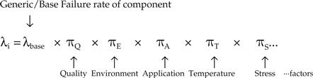
Reducing the number of variables to a few key ones for simplicity, we can write for total equipment failure rate:
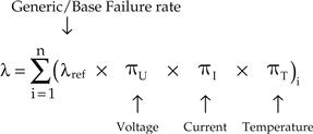
As indicated, it was common practice to get a predicted MTBF for a power supply of the order of only 100k hours by Part Stress analysis, and around 150k hours to 200k hours by Part Count analysis. Neither of these predicted numbers came close to demonstrated/field reliability numbers — which were typically 3× to 6× higher.
There are several other reliability prediction methods in use today. A popular method is the Telcordia SR-332 standard (Bellcore became Telcordia in 1997). Siemens uses SN-29500, based on IEC61709. There is also a British Telecom standard going around. Though these are in fact quite similar to the Part Stress analysis method of MIL-HDBK-217F in philosophy, they end up with very different numbers (about 3× higher MTBF). One reason for that is some of the modern methods allow for fitting test and field data to the stress models. In effect, they don’t rely on an outdated database, and therefore produce more realistic predictions than MIL-HDBK-217F.
Demonstrated Reliability Testing (DRT)
Commercial power supplies are often subjected to a pre-production DRT (Demonstrated Reliability Test). Several hundred power supplies are put in a chamber and operated at maximum load and rated operating temperature (or as stated). The number of failures occurring after a certain pre-determined time tells us with a certain “confidence level” how a much larger number of units placed in the field will perform in terms of reliability. The statistical formula for MTBF, conforming to MIL-STD-781D and MIL-HDBK-338B, is
![]()
where f is the number of failures, α is the “significance level,” related to the “confidence level” by
![]()
We need to refer to the Chi-square (χ2) numbers provided in Table 6.2.
Example:
How many POH are required to demonstrate an MTBF of 250k hours with 90% confidence (temperature specified as 55°C)?
Table 6.2. Chi-square Lookup Table.
| Number of Failures | χ2 at 60% CL | χ2 at 90% CL |
| 0 | 1.833 | 4.605 |
| 1 | 4.045 | 7.779 |
| 2 | 6.211 | 10.645 |
| 3 | 8.351 | 13.362 |
| 4 | 10.473 | 15.987 |
| 5 | 12.584 | 18.549 |
We should have 0 failures when operated for
![]()
We should have only 1 failure when operated for
![]()
Example:
How many units are required for a 4-week test to demonstrate an MTBF of 250 k hours at 60% confidence level?
At 60% confidence level, for one failure maximum, we need to accumulate
![]()
In 4 weeks we have 672 h. Thus, for a 4-week testing period we need to test
![]()
Note that these units will all need to be operated simultaneously at maximum load, or 80% of maximum load (as specified), and at maximum ambient of 55°C (or as specified). Typically, some of these will be run at customer’s location and some at the power supply manufacturer’s location. We should have at most one failure up to this point. Once that failure is analyzed and a solution put in place, it is no longer counted as a “chargeable failure” (i.e., anything of an electrical nature that can occur in the field).
Accelerated Life Testing
If failure rate rises on account of temperature, why can’t we subject a batch of power supplies to high-temperature testing, and in effect “fast-forward” through the bathtub curve of Figure 6.2 at high-speed, to accumulate data quickly on what will happen in the field when the equipment is operated at normal (lower) temperatures? Hopefully, we can then estimate both the life and the MTBF we will encounter in the field — provided we know how things scale with temperature. In other words, we need to know the (temperature) Acceleration Factor (“AF”).
That leads us to Arrhenius’ equation that describes the relationship between chemical reactions and temperature. Written in a form suitable for our purpose, it says the rate of a reaction varies as
![]()
where EA is the activation energy in eV (electron Volts), k is the Boltzmann constant, equal to 8.617×10⁻⁵ eV/K (K is Kelvin), and T is the temperature in Kelvin. Arrhenius’ equation treats every reaction/failure as the act of crossing an (empirical) energy barrier with a certain height (EA in eV). When we heat up the molecules, more and more of them get agitated enough to jump that wall and the reaction proceeds faster (i.e., more failures). Arrhenius’ equation is commonly used to estimate reliability and life.
Comparing the rate at T1 (lower) to the rate at T2 (higher), we get the Acceleration Factor as
![]()
and this is the factor by which we multiply the failure rate at the lower temperature to get the failure rate at the higher temperature.
It is commonly stated that the rule of thumb is that every 10°C rise leads to a doubling of failure rate, and also a halving of life when talking about aluminum electrolytic capacitors. That corresponds to an Acceleration Factor of 2. If we work backwards to calculate the corresponding EA, we will see that if we set T1=273+50 and T2=273+60 (50°C to 60°C), we get AF=2 for EA=0.65 eV. AF is a function of temperature. If we go from 80°C to 90°C, for the same EA, we get AF=1.8, not 2.
The doubling/halving rule every 10°C therefore implies an assumed EA of about 0.65 eV. But activation energies encountered, in general, can typically vary anywhere between 0.3 eV and 1.2 eV. If EA is 0.3 eV for a particular failure mechanism, then in going from 50°C to 60°C, its Acceleration Factor is only 1.4, and that drops to 1.3 from 80°C to 90°C.
In performing actual reliability tests, there are two main categories:
(a) Accelerated Life Testing (ALT): Though the word used here is life, this test involves raising the temperature and using Acceleration Factors to predict both the life and the MTBF at lower temperatures. This has to be done cautiously so we do not introduce new failure modes that would not have been present at normal lower temperatures.
(b) Accelerated Stress Testing (AST): The purpose of this test is usually not intended to be predictive in nature. Here, we just try to precipitate failures by increasing stresses with the intention of uncovering basic weaknesses.
Under the sub-category of AST, we can perform the following tests:
(1) Highly Accelerated Life Test (HALT): This is a development tool performed on equipment (e.g., power supply). Its purpose is to identify weaknesses during the design phase itself, so improvements can be carried out, cost permitting. It is also called STRIFE (for Stress and Life Test).
(2) Highly Accelerated Stress Screen (HASS): This is a production screen for manufactured equipment. Samples from production can be subjected to very high stresses for a short time to uncover weaknesses in the manufacturing process (or in design).
(3) Highly Accelerated Stress Test (HAST): This is a component-level test. Samples are subjected to extreme environmental stresses (temperature, pressure, and/or humidity) to uncover weaknesses. Semiconductors are commonly subjected to this during qualification.
In doing accelerated testing we have to be very careful we are only accelerating known failure modes, not creating new ones. In other words, our hope of doing a “fast-forward” cannot be as fast as we had perhaps hoped for.
With that, we have completed our discussion on reliability and stresses, and we now discuss life prediction of aluminum caps.
Part 3: Life Prediction of Aluminum Electrolytic Capacitors
Aluminum electrolytic capacitors, with all their advantages, are subject to slow deterioration (aging) caused by gradual evaporation of the electrolyte inside. That process is accelerated by heat generated inside the capacitor (due to self-heating) and around it too (from nearby hot components). The internal heat is the RMS current squared (calculated in Chapter 7) multiplied by the ESR of the capacitor. Though the capacitor is supposedly sealed to prevent escape of the electrolyte, no joint is 100% hermetic. Therefore, aging is a slow but inevitable process, and eventually determines the useful life of the capacitor. But we also have to be clear how we define “useful life.” For example, we can always choose to declare the retirement age of an individual as 55 years, or 60 years, or even 65 years. But we have to ask what really makes sense, in terms of performance, for capacitors as for humans?
Looking at capacitor datasheets we see that a typical aluminum electrolytic capacitor has a declared life (“LO”) of 2,000 hours–5,000 hours (recently, Panasonic for example announced 105°C caps with 10,000 hours life). Since there are 365×24=8,760 hours in one year, that would make any equipment containing such capacitors last less than a year. Clearly that is not enough. Typical power supply specifications call for a minimum life of 44k hours (5 years) when operated at 40°C ambient (assuming 24-hour operation).
Now we look at the fine print of the capacitor datasheet. It says the end of useful life of an aluminum electrolytic cap is defined as a certain percentage decrease in capacitance (typically 20%) and/or a certain percentage increase in its “Dissipation Factor” (typically 200% or 300% of initial value). It clarifies that the declared useful life (2,000 hours or 5,000 hours, for example), is obtained by operating the capacitor at its maximum rated temperature (typically, the upper rated category temperature, UR, which is 85°C or 105°C), and by passing a low-frequency current (typically, 120 Hz) with an RMS value set equal to its declared Ripple Current Rating IR.
First, let us be clear what Dissipation Factor is. By definition, DF (or tan δ), is related to the ESR by
![]()
or
![]()
where
![]()
So, Dissipation Factor is the ratio of the real part of the impedance (resistance, i.e., ESR) to the Reactive Impedance (1/Cω). It is therefore a measure of how bad a cap is, that is, its loss term versus its energy storage capability (measured at 120 Hz). It is the reciprocal of the quality factor Q. So a high DF indicates a bad cap in terms of a high ESR. Note that though electrolytic capacitors have much higher ESR than ceramic or film caps, they thankfully have much higher Capacitance/Volume.
If capacitance falls by 20% and DF goes up 200%, as per worst-case end-of-life limits, the ESR would have gone up 2.5 times
![]()
Further, though capacitance goes down from its initial value by only 20% by end-of-life, we have to keep in mind that its initial (starting) value itself may have been 10% or 20% lower than the nominal value, on account of typical capacitor tolerances. We may therefore have to keep the worst-case end-of-life capacitance value in mind upfront while selecting aluminum electrolytic capacitors, especially if capacitance is a key parameter/requirement in our selection process. But certainly, the ESR goes up significantly as the electrolyte evaporates. Further, after the end-of-life threshold, there is a rather rapid increase in ESR. And since higher ESR causes more heating, more heating causes more wearout (and therefore higher ESR). There can be a runaway condition thus established that could mark the end-of-life of the converter too, shortly. So, aging is a real concern when using aluminum electrolytics, and lifetime estimates are therefore important. After all, the life of the equipment is determined by the component with the shortest life. That can be the aluminum electrolytic unfortunately.
In Figure 6.3, we present a simplified thermal model of an aluminum electrolytic cap. The ripple current rating IR is so chosen, that when IR is passed through the cap, it produces a certain optimum delta between ambient and case, and also from case to the core (deep inside the capacitor). Further, these two deltas, that is, from ambient to case and from case to core, are assumed to be the same (usually). That optimum delta is set to 5°C for 105°C capacitors and 10°C for 85°C capacitors. So, if we place a 105°C rated cap at an ambient temperature of 105°C, and pass IR through it, its core will be at exactly 115°C. In other words, the stated life of the cap (LO), 5,000 hours for example, is the life of the cap with its core held at 115°C. Similarly, if we pick an 85°C cap, its datasheet life figure LO is at a core temperature of 105°C. If we lower the ambient by 20°C, the core temperatures will fall to 115–20=95°C and 105–20=85°C, respectively. This leads to a significant increase in life since the evaporation of the electrolyte slows down. The well-known lifetime doubling rule is that every 10°C fall in core temperature leads to a doubling of life.
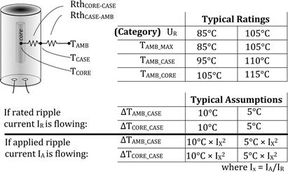
Figure 6.3: The capacitor model and ratings for understanding lifetime prediction.
One problem is: as users, we have no way of measuring core temperature to estimate life accurately. So we need to turn to the vendor for guidance. Most vendors agree to the following simplified, user-friendly formula to estimate life (L). This is
![]()
where
![]()
ΔTrated is the optimum differential we talked about previously (5°C for 105°C caps). ΔTCORE-CASE is the actual delta in the application (case to ambient as well as core to case). The above formula tells us that whereas a fall in ambient temperature doubles life every 10°C, if the delta is more than the optimum (ΔTrated), then the life halves every 5°C by which the delta exceeds the optimum delta. Since heating is proportional to RMS-squared, the actual delta in the application can be estimated by
![]()
Here, IA is the applied RMS and IR the rated RMS. Also, since there may be local heating from adjacent components, the TAMB to be used in the above equation is taken to be TCASE, and that provides roughly a 5°C safety margin when using 105°C capacitors. Also, for scaling purposes, it is nice to talk in terms of ratios and multipliers. So finally, a usable formula is
![]()
where LX is the lifetime multiplier, and IX=IA/IR
This is the formula used in the Mathcad worksheet in Figure 6.4 to plot the accompanying curve (plotted out for 105°C caps).
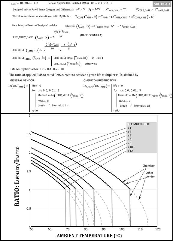
Figure 6.4: Mathcad worksheet and design chart for estimating life multipliers (105°C cap).
To use the curves, keep in mind that life increases toward the left, and decreases towards the right. So, for example, if we have a 5,000 hours/105°C cap at an ambient of 55°C, and we pass 1.5 times the rated ripple current, we expect the life to exceed 12×2,000=60,000 hours. This is 60,000/8,760=6.85 years. A typical requirement for most equipment is only 5 years.
Note that Chemicon is considered more conservative than most vendors. Naturally, it places one more restriction: though the cap life halves every 5°C by which we exceed the rated ΔT, we cannot expect that if we reduce the delta to less than the rated ΔT, that the sign will flip in the equation above, and we can thus claim (or expect) higher life. Chemicon refuses to buy into that! That is why in Figure 6.3 we have a distinct Chemicon boundary in solid black/gray. The dashed gray lines (or something close to these) are published by other vendors, and you can use those curves at your own risk.
A numerical example is provided below.
Example:
We are using a 2,200 μF/10 V capacitor from Chemicon. Its catalog specifications are 8,000 hours at maximum rated 1.69 A, stated at 105°C and 100 kHz. The measured case temperature in our application is 84°C and the measured ripple current is 2.2 A. What is the expected life?
![]()
where
![]()
Therefore, since (8.473–5)/5=0.695, we get
![]()
Since the internal delta is 8.473°C, that is, greater than 5°C, the above estimate is valid for capacitors from most other vendors too.
One question often asked is can we use forced air cooling to enhance the life of a capacitor? Some vendors provide guidelines how to estimate life under these conditions, but some staunchly resist publishing any such life estimates, or at least standing firmly behind them. In effect, most vendors say you can use life predictions under forced air flow at your own risk. The reason is it is very hard to predict the core temperature under such variable conditions. The actual air flow itself is hard to know accurately in the vicinity of the capacitor on a real board.
Lastly, keep in mind that the declared ripple current rating is usually stated at 120 Hz. Since ESR (and heating) reduces with frequency, vendors provide frequency multipliers. A typical high-frequency multiplier is 1.43 at 100 kHz. So, for example, if the capacitor is rated 1.5 A RMS at 120 Hz, its ripple current rating (in modern switching power supplies) is 1.5×1.43=2.145 A. That is the number we should use for IR in the calculations above. There is no other change.