
5 Technology for Telecommunications: Integrated Optics and Microelectronics
5.1 Introduction
In Chapter 4 we have presented a survey of fiber technology and of the technology needed to fabricate optical filter and wavelength multiplexer and demultiplexers for telecommunications.
In this chapter we will present a survey of the so-called integrated technology that is the technology leveraging planar processes to manufacture electronics and optical components.
The first part of the chapter is devoted to optical planar components built on the III–V platform.
The most important of those components is the semiconductor laser, both for the huge number of telecom and non-telecom applications and for the key role it plays in telecom equipments.
We will not try to make a survey of the semiconductor laser technology per se, but we will only summarize the characteristics and the main evolution potentialities of the devices used in telecommunications.
These devices are essentially signal sources or pump lasers for fiber amplifiers and we will consider both the applications, which require quite different devices.
We will add here also a brief description of the linear characteristics of semiconductor optical amplifiers (SOAs), which will be considered for the potentialities related to their nonlinear behavior in Chapter 10.
After a brief analysis of the modulators, both from III–V materials and from lithium niobate (LiNbO3), the first part of the chapter devoted to planar optics comes to an end.
In the second part of the chapter we will analyze the impact of electronic evolution on telecommunication equipments.
Electronics is by far the most important technology used in telecommunication equipments and modern telecommunications would be unconceivable without very large-scale integrated circuits.
Naturally it is not possible to make a review of electronics technology from first principles, and we will assume that the reader has already a familiarity with basic electronics principles and potentialities.
Thus only the most recent electronic development that has an impact on telecommunications will be reviewed, excluding wireless technologies, both traditional radio bridges and wireless access in all its different standards.
After a brief review of the evolution of the complementary metal oxide semiconductor (CMOS) transistors, the base element of electronic circuitry, the discussion on electronics is divided into the analysis of error correction and compensators for transmission systems and the analysis of the base elements of electronics switching.
Only the analysis of the switch fabric itself, starting from the elementary cross-point, is delayed to Chapter 7, in the more suitable framework of the switching and routing machine architectures.
5.2 Semiconductor Lasers
5.2.1 Fixed-Wavelength Edge-Emitting Semiconductor Lasers
Semiconductor lasers are the most diffused laser category, whose application ranges from consumer products (like compact disc players) to highly specialized industrial applications like transmitters in optical fiber systems and sensor equipment [1].
Here we will limit our review to two categories of semiconductor lasers that are instrumental in developing optical transmission systems: transmission lasers and pump lasers.
Transmission lasers are used to provide the optical carrier over which the information is coded.
Different applications have different requirements for the optical carrier parameters like power, linewidth, wavelength stability, and so on, as well as different cost targets; thus there are a wide variety of transmission lasers.
Depending on the specific application, the modulation of the carrier can be performed by an external modulator (a component completely different from the source laser), by a modulator integrated into the same chip of the laser or by the laser itself, with the so-called direct laser modulation.
Something similar happens for pump lasers, whose application ranges from the cheap erbium-doped fiber amplifiers (EDFAs) that could be used in the optical access network to the high-performance distributed Raman amplifiers used in ultra-long haul dense wavelength division multiplexing (DWDM) systems.
5.2.1.1 Semiconductor Laser Principle
The principle at the base of the working of a semiconductor laser is to create population inversion between valence and conduction electrons (or holes, depending on the material), exciting electrons from the valence to the conduction band of a semiconductor via current injection.
In order to achieve photon-stimulated emission, the transition between valence and conduction bands corresponding to the desired laser frequency has to be a “direct transition.”
This means that pseudo-electrons in the valence and conduction bands must have the same crystal momentum so that decay can happen with photon emission without the need of higher-order processes to compensate the momentum difference. In Figure 5.1 [2] the band structure of silicon, characterized by an indirect transition between the valence and the conduction band, is shown, while the band structure of an InGaAs alloy [2], characterized by a direct transition in the near-infrared region, is shown in Figure 5.2.
The requirement of direct transitions practically selects the materials that are suited to build semiconductor lasers: they are essentially the alloys of III–V semiconductors, starting from GaAs and GaAsP, used for pump lasers, to InGaAsP, which is generally the alloy in the active region of lasers used for transmission.
Once the material is selected, a structure suitable for electron pumping has to be realized. The best possible structure is an inversely polarized p–n junction. In a p–n junction under inverse polarization, the field in the junction zone is opposite to the electron flux; thus if a current is pumped in the junction, electrons pass through being promoted to higher-energy levels to overcome the junction potential barrier. In this condition the average population of the conduction band can become greater than the population of the valence band, thus causing population inversion.
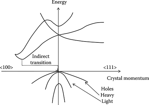
Figure 5.1 Schematic representation of the band structure of silicon.
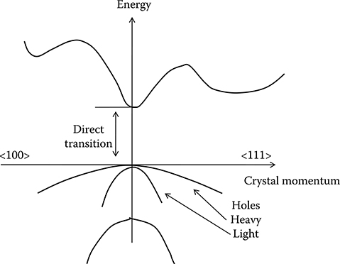
Figure 5.2 Schematic representation of the band structure of a II–V alloy having direct optical transition at the band gap.
However, if a simple junction is used, creating the conditions for lasing operation is quite difficult.
As a matter of fact, in a structure like that of Figure 5.3, there is no lateral confinement either for the injected current or for the optical field. Thus on the one hand, there is a constant electron loss due to the leak current flowing away from the inversion zone on the side of the device and, on the other hand, the optical mode is very large and the superposition of the mode with the inverted area of the junction where optical gain is concentrated is quite scarce.
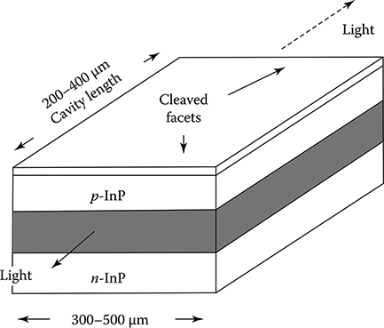
Figure 5.3 Simpler possible structure of a semiconductor laser.
In order to achieve effective lasing operation, both the current and the optical mode have to be effectively confined in the junction area.
Several architectures have been proposed to achieve vertical and lateral confinement, at present the most used solution is constituted by heterostructure index–guided architecture [1].
The heterostructure solution consists in realizing a p–i–n junction where the neutral zone is realized in a different alloy with a smaller band gap with respect to the doped zones. The band profile across the heterostructure is shaped approximately as shown in Figure 5.4 when an inverse polarization is applied.
The fact that the intrinsic material has a smaller energy gap with respect to the surrounding doped layers creates a sort of trap for the injected carriers: when the carriers arrive in the intrinsic zone, they fall in the potential energy hole and are confined to the intrinsic zone.
If the heterostructure provides confinement in the direction of the current injection, confinement in the lateral direction has to be achieved via some other system.
The most used structure for lateral confinement is the so-called index-confined architecture, where the optical mode is confined in the laser-active region by realizing an optical waveguide whose core is the active region itself. In this way the different materials provide confinement of the current and the diffraction index difference provides confinement of the field in the same region.
A transversal section of a buried heterostructure laser is represented in Figure 5.5. The gray area represents the active waveguide that is buried below the surface structure and assures contemporary good lateral current confinement and good superposition between the optical mode and the inverted region.
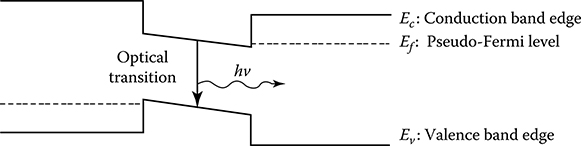
Figure 5.4 Schematic band profile of a heterojunction in inverse polarization.
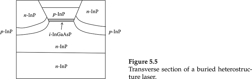
Figure 5.5 Transverse section of a buried heterostructure laser.
Once inversion is effectively realized, in order to start the lasing operation, a positive counterreaction has to be introduced via an optical cavity to sustain spontaneous oscillations of the structure.
The easier way to do this is to cleave the front and rear facets of the laser to create a reflectivity.
The inner laser waveguide behaves like a Fabry–Perot (FP) cavity assuring the needed feedback to the laser.
The structure of an FP laser is schematized in Figure 5.3. With the typical dimensions of semiconductor lasers, the FP cavity has a free spectral range so small that several modes are enhanced by the optical gain.
Thus in general, FP semiconductor lasers oscillate in multimode regime even if, with some care in designing the laser, few modes can be selected. Even when single-mode operation is achieved by using strongly wavelength-dependent mirrors (that can be realized by multiple layer coating of the FP facets) this is not a stable condition and side modes can start to oscillate due to environmental fluctuations or laser modulation.
In order to achieve real single-mode operation a strongly wavelength-selective feedback has to be introduced.
This can be done in several ways, among which distributed feedback (DFB) is by far the most used.
5.2.1.2 Semiconductor Laser Modeling and Dynamic Behavior
Once confinement is achieved both for the optical field and for the injected charges, the laser can be considered as a waveguide inserted into a resonant cavity with the core subject to population inversion to generate optical gain.
A physical modeling of the semiconductor laser would require a quantum representation of both the optical field and the pseudo-particle population inside the crystal.
In this way the laser equations will appear as a couple of interacting equations, one for the density matrix elements representing the electron population and the other for the quadrature operators of the field [3].
Even though this analysis is possible, it is quite complicated and, from the point of view of the physical comprehension of laser dynamics, is not more effective with respect to a semiclassical model.
In a semiclassical model, the laser behavior is represented with a set of rate equations for the propagating field and for the carrier density.
The only element that cannot rise from a semiclassical analysis is the spontaneous emission noise, which is a pure quantum element (compare Section 4.3.1.1). Thus the noise terms have to be added phenomenologically to the semiclassical rate equations [4].
With this in mind, the rate equations can be derived by the coupled field wave equation and electrons balance equation and by applying the slowly varying and rotating wave approximation to the wave equation [5].
At the end of these procedures, calling N(x,y,z,t) the carrier population in the conduction band, S(x,y,z,t) the optical energy inside the cavity, which is proportional to the photon density, and ϕ(x,y,z,t) the field phase, the coupled equations of a semiconductor laser can be written as
∂N∂t+DN∇2N=1qda−GN(N−N0)s(1+ɛs)−NτN+FN∂P∂t=γGN(N−N0)s(1+ɛs)−sτp+ħω0Rsp+ħω0Fs∂ϕ∂t=−(ω0−Ω)+α2[γGN(N−N0)−1τN]+Fϕ(5.1)
(5.1)
The symbols that appear in the rate equations have the following meanings:
DN is the carrier diffusion coefficient. In many problems the carrier density can be considered approximately constant in the active region and zero elsewhere, thus neglecting the diffusion term DN ∇ 2N and the dependence of N from the spatial coordinates.
J is the pumping current.
da is the active layer thickness.
q is the electron charge.
τN is the carrier’s lifetime.
GN is the population inversion induced gain.
(N − N0) is the population inversion factor.
Ɛ is the gain saturation constant.
τP is the photon’s lifetime.
γ is the confinement factor, that is, the ratio between the active region volume and the modal volume. This parameter is evaluated by solving the mode propagation into the active region.
ω0 is the angular frequency of the optical field.
Ω is the resonance frequency of the laser cavity.
Rsp is the spontaneous emission rate.
α is the so-called linewidth enhancement factor. The fundamental limit for the linewidth of a free-running laser is provided by the Schawlow Townes formula. Semiconductor lasers exhibit significantly higher linewidth values due to a coupling between intensity and phase noise, caused by the dependence of the refractive index on the carrier density. In the semiclassical model, the linewidth enhancement factor α quantifies this amplitude–phase coupling mechanism; essentially, α is a proportionality factor relating phase changes to changes of the amplitude gain [6].
Fj, j = S, N, ϕ are the noise terms that are added phenomenologically to the rate equations. These are independent random processes whose first moments have to be determined from the results of the quantum theory. In particular we have
〈Fj(t,x,y,z)〉=0j=S,N,ϕ(5.2)
![]()
(5.2)
〈Fj(t,x,y,z)Fk(t′,x′,y′,z′)〉=Djkδj,kδ(t,t′)δ(x,x′)δ(y,y′)δ(z,z′)(5.3)
![]()
(5.3)
Djk are the elements of the so-called diffusion matrix which, in the framework of the semiclassical approximation, can be written as
D=(DSSDSNDSϕDSNDNNDNϕDSϕDNϕDϕϕ)=(RspS−RspS0−RspSRspSħω0+NτN000ħω0Rsp4S)(5.4)

(5.4)
Realistic values of the parameters of a standard DFB laser used as a source in DWDM systems are reported in Table 5.1.
To describe the laser behavior on the grounds of Equation 5.1 what we have assumed up to now is not sufficient.
As a matter of fact, these equations are stochastic equations that cannot be solved if the distribution of the noise term is not known.
The most correct distribution of the terms Fj (j = S, N, ϕ) is not Gaussian: it is sufficient to consider that the term representing the shot noise (i.e., the fluctuation of the optical power) should be distributed following a Poisson distribution.
However, in the case of a stable lasing operation, it is possible to demonstrate that, due to the fact that the number of excited carriers and of the photons is very high, the Gaussian approximation implies a small error, in line with the overall accuracy of the semiclassical model.
Starting from Equations 5.1 and from the laser structure the main characteristics of a specific type of semiconductor laser can be derived. Despite the intrinsic complexity of their behavior, gain saturation happens also in semiconductor lasers.
In particular, due to the presence of the saturation constant, increasing the power in the cavity, the laser inner gain decreases so that the dependence of the emitted power from the pump is not exponential as foreseen in a laser without gain saturation.
Moreover, the dependence of the carrier density on a temperature typical of a p–i–n junction induces a sensible dependence of the curve relating the pumping current and the emitted power on temperature.
TABLE 5.1 Values of the Microscopic Parameters of a DFB Used at the Transmitter in DWDM Systems

A typical emitted power versus current characteristic of a DFB laser is shown in Figure 5.6. From the figure, the laser threshold, the dependence of the laser behavior on temperature, and the saturation of the cavity gain are evident, so that at each temperature a maximum emitted power exists at the edge of saturation.
Above the maximum emitted power, the gain saturation drives a decrease of the emitted power while increasing the driving current.
When emitting in continuous wave (CW) mode, a semiconductor laser is affected both by phase and by intensity noise due to the amplified spontaneous emission into the laser cavity and to the fluctuations of the carrier density.
The noise characteristics can be obtained from the rate equations with a perturbation approach, at least as far as the noise is small [7]. In particular, substituting the variables of the rate equations the following expressions
N=N0+δNS=S0+δSϕ=ϕ0+δϕ(5.5)
(5.5)
where N0, S0, and ϕ0 are the stationary solutions of the rate equations without noise, and linearizing with respect to the noise terms, the noise statistical characteristics can be derived.
In particular, the linearized equations assume a simpler form by introducing the vector ˉX=(S,N,ϕ)![]() and the matrix
and the matrix
Γ=(ΓSSΓSNΓSϕΓNSΓNNΓNϕΓϕSΓϕNΓϕϕ)=(∈S0τP(1+∈S0)γGNS0ħω0(1+∈S0)01τP(1+∈S0)1τN+γGNS0ħω0(1+∈S0)00αγGN20)(5.6)

(5.6)

Figure 5.6 Typical emitted power versus current characteristic of a DFB laser.
In order to evidence the macroscopic noise terms in the expression of the emitted field, it can be written as
→E=√P0a(x,y)r(t)eiωt+φ(t)→x=√ℑS0τca(x,y)√(1+δSS0)eiωt+[ϕ(t)+Ψ]→x(5.7)

(5.7)
where
r(t) and φ(t) are the relative intensity noise (RIN) and the phase noise
ℑ is the end mirror transmittance
τc is the cavity round trip time that allows us to pass from internal energy to emitted power
ψ is the phase contribution of the extraction mirror
The power spectral density of the RIN is given by
RIN(ω)=ħωS202DNNΓ2SN+2DSS(Γ2NN+ω2)+4DSNΓSNΓNN[(Ω2R−ω2)2+ω2(ΓNN+ΓSS)2](5.8)

(5.8)
where it is not difficult to recognize the typical behavior of a resonance, whose natural frequency is Ω2R=(ΓSSΓNN+ΓSNΓNS)![]() and whose dumping rate is (ΓNN + ΓSS).
and whose dumping rate is (ΓNN + ΓSS).
The observation that the laser behavior is characterized by a dumped resonance is very general, not limited exclusively to the RIN spectrum.
As a matter of fact, the same behavior is exhibited by the frequency noise (i.e., the process ˙φ=δφ/δt![]() ), whose power spectral density is given by [8]
), whose power spectral density is given by [8]
F˙φ(ω)=Dφφ+Γ2φN[DNN(Γ2SS+ω2)+Γ2NSDSS−DSNΓSSΓNS][(Ω2R−ω2)2+ω2(ΓNN+ΓSS)2](5.9)
(5.9)
Besides the presence of the laser characteristic resonance, the expression of the frequency noises spectrum allows also the other typical diode laser mechanism to be evidenced.
As a matter of fact, it is made by two terms: the first is due to the phase of random emitted photons, and the second is proportional through Γ2φN![]() to α2 and represents the additional phase noise due to the coupling between amplitude and phase through the carrier density [9].
to α2 and represents the additional phase noise due to the coupling between amplitude and phase through the carrier density [9].
The power spectral densities of the RIN and of the phase noise for a typical DFB laser emitting at 1550 nm are represented in Figures 5.7 [10] and 5.8 respectively.
From the theory we have presented, it results that the same phenomenon causes both the excess RIN and the excess phase noise with respect to the quantum limit. Thus a relationship must exist between the RIN and the phase noise spectra.
This relationship can be obtained by simplifying the denominator in the expressions of the two spectra and deriving an expression for the relation between them.
This expression can be experimentally verified by passing from the phase noise to the linewidth that is one of the most commonly measured quantities in a laser.

Figure 5.7 Power spectral density of the RIN for a typical DFB laser emitting at 1550 nm.
(After Aragon Photonics Application Note, Characterization of the main parameters of DFB using the BOSE. 2002, www.aragonphotonics.com [accessed: May 25, 2010].)
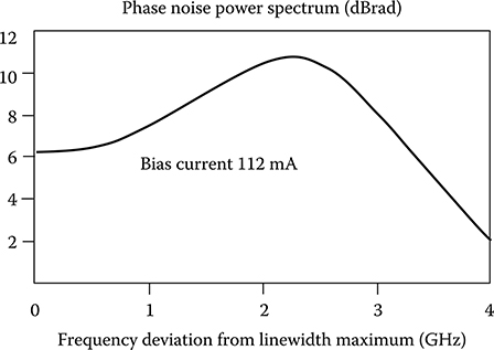
Figure 5.8 Power spectral density of the phase noise for a typical DFB laser emitting at 1550 nm.
(After Travagnin, M., J Opt. B. Quant. Semiclass. Opt., 2, L25, 2000.)
A rigorous derivation of the laser linewidth that is possible starting from (5.9) [8] would conclude that the laser linewidth is not Lorentian, but is composed by a Lorentian lobe plus two side peaks far from the central wavelength, exactly the frequency of relaxation oscillations. However, in high-quality lasers these lobes are so reduced that a Lorentian approximation of the linewidth is more than accurate.
Assuming a Lorentian linewidth, the expression of the full width at half maximum (FWHM) is given by
Δv=Rsp(1+α2)(4πr)(5.10)

(5.10)
where r is the cavity refraction index.
The curve relating the linewidth and the maximum of the RIN spectrum is shown in Figure 5.9 besides a set of experimental points from [11]. In particular the theoretical curve is obtained by best fitting the experimental data.
Another important characteristic of the semiconductor lasers is that they can be directly modulated acting on the bias current. However, when the bias current fluctuates, a complex dynamical behavior is observed, mainly due to the coupling between field amplitude and phase and to the resonance at ΩR.
This phenomenon causes the contemporary presence of intensity and phase modulation, which always creates a frequency chirp in the direct modulated pulse train.
Besides this fundamental effect, a second phenomenon constraining the direct modulation bandwidth of semiconductor lasers is the presence of parasitic capacities in the structure. Reducing them is a key issue to increase the direct modulation bandwidth.
Considering again the rate equations with spatially constant variables and neglecting the noise terms, it is possible to study direct modulation by applying the substitutions in Equation 5.5 where now the fluctuations are due not to the noise but to the modulation.
In this condition the equations can be linearized again around the laser bias point. In this case Equation 5.7 can be used to pass from the field into the cavity to the emitted field so that the modulation index (i.e., the derivative of the emitted optical power with respect to the pump current fluctuations) results:
δPδJ=−ħωqdaℑτNΓNSω2m−Ω2R+iωm(ΓNN+ΓSS)(5.11)

(5.11)
where ωm is the modulation frequency. The presence of the natural laser resonance is always evident and in this case it limits the modulation bandwidth.
If the expression of the coefficients Γkj is substituted in Equation 5.11 it is evident that, besides the presence of a resonance, gain saturation (represented by the factor ε also contributes to shrink the bandwidth with respect to the theoretical limit, and that higher the gain saturation coefficient, the smaller is the modulation bandwidth.
Similarly to the power modulation index, a frequency modulation index can be evaluated whose expression is

Figure 5.9 Linewidth versus RIN spectrum peak relationship for a DFB laser.
(After JDSU Application Note, Relative Intensity Noise, Phase Noise and Linewidth, JDSU Corporate, s.l., 2006, www.jdsu.com [accessed: May 25, 2010].)
δ˙ϕδJ=ΓϕNδNδJ(5.12)

(5.12)
Equation 5.12 represents the theoretical frequency response of a semiconductor laser that is responsible for both the possibility of modulating the output field frequency by modulating the bias current (property exploited for example to implement the Brillouin dither) and the chirp that unavoidably is present when the laser is directly modulated.
Equation 5.12, however, due to all the approximations that are the base to derive the rate equations, does not take into account several phenomena that cause the deviation of the frequency response of real lasers from the simple proportionality to the carrier density variations.
Generally the frequency response is almost flat up to the resonance of the laser, but here it shows the resonance effects through a peak and then decreases rapidly.
5.2.1.3 Quantum Well Lasers
A quantum well laser is a laser diode in which the active region of the device is formed by one or more regions so narrow that quantum confinement occurs, alternated by wider regions of higher bandgap.
The carriers in the active region are generally divided into two populations that occupy a completely different set of energy levels: carriers in the wells and carriers out of the wells.
Carriers out of the wells are ordinary pseudo-particles obeying the rules of carrier motion in crystals, and in particular they cannot have any energy in the forbidden band of the semiconductor forming the active region.
Inside the quantum well, quantum confinement of the carriers creates energy sub-bands inside the forbidden energy band. The central energy of the sub-bands depends on the well thickness.
This is easily understood remembering that in the simple case of a one-dimensional infinite energy well the energy levels of a particle are equal to En = n2(ħ2π2/8mL2 ), where n is the quantum number and L is the width of the well.
Due to these characteristics the wavelength of the light emitted by a quantum well laser is determined by the width of the active region rather than just the bandgap of the material from which it is constructed. This means that much shorter wavelengths can be obtained from quantum well lasers than from conventional laser diodes using a particular semiconductor material. The efficiency of a quantum well laser is also greater than a conventional laser diode due to the stepwise form of its density of states function.
Beside the use of a quantum well, in order to shape the energy levels inside the active region, the so-called strain technique can be incorporated.
This consists in introducing in the quantum well zone a tensile or compressive strain, whose effect is to change the conduction sub-bands due to the quantum well.
One of the main effects of a controlled strain is to reduce the threshold current of the laser due to the increased separation between energy bands that renders recombination more difficult [12].
5.2.1.4 Source Fabry–Perot Lasers
Probably FP semiconductor lasers used as signal sources are the lasers produced in larger volumes on the market for a huge number of applications, from telecommunications to consumer electronics to sensors and so on.

Figure 5.10 Spectrum of an FP InGaAsP laser emitting in a quasi-single-mode regime.
In telecommunications such lasers are adopted at transmitters either to generate the carrier or to generate the information-carrying signal through direct modulation when single-mode laser operation is not required but the cost of the source is a key issue. As a matter of fact, due to the simpler structure and the great volume production, FPs are cheaper with respect to single-mode lasers like DFB.
Thus, FPs are the standard optical sources in several types of access systems, from point-to-point to A and B class G-PON. Moreover, such lasers are used in the low-performance client cards of transmission systems, where it is needed to connect systems in the same central office and the connection speed is not so high.
The typical emission spectrum of an FP InGaAsP laser emitting in a quasi single-mode regime is plotted in Figure 5.10. The side modes suppression ratio (SMSR) is about 19 dB, which is much lower than the typical 35–40 dB of a DFB laser, but is enough for several applications, especially if the laser has not to be modulated.
The presence of a few lasing modes in an FP laser generates the growth of a particular noise phenomenon when it is directly modulated: the mode partition noise [13].
Mode partition noise is due to the random fluctuations of the lateral modes that causes a change in the spectrum and a fluctuation in the power of the main mode due to the fact that the steady-state power emitted from the laser in a first approximation is constant and depends only on the pump and on the laser quantum efficiency.
The effect is an enhancement of the RIN well above the limit given by the spectrum in a strict single mode operation. This effect is shown in Figure 5.11 where the fact that the sensible amount of RIN is mainly due to the mode partition noise is clear from the form of the RIN spectrum.
A selection of characteristics of practical FP diode lasers for different applications is reported in Table 5.2. From the table the wide span of applications covered by FP lasers corresponding to the possibility of matching different set of requirements is evident.
5.2.1.5 Source DFB Lasers
In a DFB laser the feedback is obtained by building a grating immediately on top of the active zone or on the side of it, influencing the propagation of the tail of the guided mode. Via interaction with the mode tail, the grating blocks the amplification of all the wavelengths, save the one resonating with the grating itself, thus guaranteeing single-mode operation.

Figure 5.11 RIN spectrum induced by relevant mode partition noise in a multimode FP laser.
(After Wentworth, R. H. et al., J. Lightwave Technol., 10(1), 84, 1992.)
TABLE 5.2 Characteristics of Practical FP Diode Lasers for Different Applications

The scheme of a DFB semiconductor laser is shown in Figure 5.12 while its single-mode spectrum is shown in Figure 5.13.
Altering the temperature of the device causes the pitch of the grating to change due to the dependence of the refractive index on temperature. This dependence is caused by a change in the semiconductor laser’s bandgap with temperature and thermal expansion.
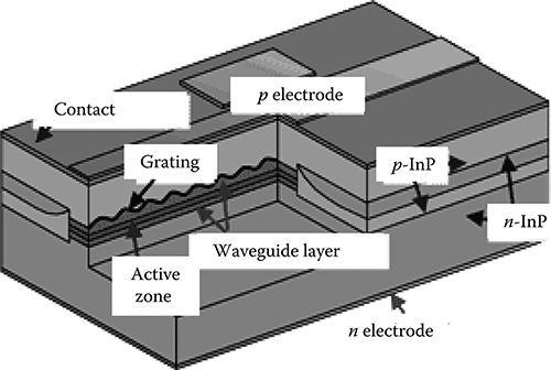
Figure 5.12 Schematic section of a high-performance DFB laser.

Figure 5.13 Emission spectrum of a typical DWDM DFB.
A change in the refractive index alters the wavelength selection of the grating structure and thus the wavelength of the laser output, producing a narrow band wavelength tunable laser.
The tuning range is usually on the order of 6 nm for an ∼50 K (90°F) change in temperature, while the linewidth of a DFB laser is on the order of a few megahertz. Altering of the current powering the laser will also tune the device, as a current change causes a temperature change inside the device.
If this temperature sensitivity can be exploited to tune the laser on the opportune wavelength, it also implies that, in order to match the stability requirements of high-performance DWDM systems, the laser has to be temperature-stabilized. This is generally done through a Peltier temperature controller and a feedback control loop that assure sufficient temperature stability in the face of environment changes and the device heat production during working.
TABLE 5.3 Characteristics of Practical DFB Lasers for Use as Sources in Telecommunication System
There are generally two distinct types of DFB lasers. Traditionally, DFBs are antireflection-coated on one side of the cavity and coated for high reflectivity on the other side (AR/HR). In this case the grating forms the distributed mirror on the antireflection-coated side, while the semiconductor facet on the high reflectivity side forms the other mirror. These lasers generally have higher output power since the light is taken from the AR side, and the HR side prevents power being lost from the back.
Unfortunately, during the manufacturing of the laser and the cleaving of the facets, it is virtually impossible to control at which point in the buried grating the laser cleaves to form the facet. So sometimes the laser HR facet forms at the crest of the buried grating, and sometimes on the slope. Depending on the phase of the grating and the optical mode, the laser output spectrum can vary. Frequently, the phase of the highly reflective side occurs at a point where two longitudinal modes have the same cavity gain, and thus the laser operates at two modes simultaneously. Thus such AR/HR lasers have to be screened at manufacturing and parts that are multimode or have poor SMSR have to be scrapped. Additionally, the phase of the cleaving affects the wavelength, and thus controlling the output wavelength of a batch of lasers in manufacturing can be a challenge.
An alternative approach is a phase-shifted DFB laser. In this case both facets are antireflection-coated and there is a phase shift in the cavity. This could be a single 1/4 wave shift at the center of the cavity, or multiple smaller shifts distributed in the cavity. Such devices have much better reproducibility in wavelength and theoretically they are all single mode, independent of the production process.
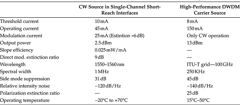
A selection of characteristics of practical DFB lasers for use as sources in telecommunication system is reported in Table 5.3.
5.2.2 High-Power Pump Lasers
If the ability to produce laser diodes with a strictly monochromatic output field that are stable in wavelength and power is instrumental to design optical transmitters for DWDM systems, high-power durable pump lasers are equally instrumental to realize optical amplifiers.
The success of fiber amplifiers, both based on erbium-doped fibers and Raman effect, is largely due to the availability of high-power laser diodes at suitable pump wavelengths.
Considering laser diodes designed to pump optical amplifiers, the key performances to care for are the emitted power, the stability of the wavelength, and the ability to emit a mode that can be focused easily on the small spot represented by a fiber-optic core.
Reliability is also a key property of these lasers, due to the fact that the reliability of the whole amplifier is largely determined by the reliability of the pumps.
The lifetime of semiconductor lasers decreases more than linearly, increasing the average emitted power, due to the fact that the more photons are present inside the laser cavity, the faster is the growth of fabrication micro-defects up to a state where they thwart the laser working.
Thus a major challenge for the manufacturers of pump lasers is to assure a long lifetime without scarifying the emitted power.
Another key design point for this type of lasers is the power consumption, which has to be limited as much as possible.
For this reason, it is important to have a high number of degrees of freedom in designing pump lasers, a condition that is assured by the use of not only a carefully selected alloy of III–V semiconductors for each laser section, but also a strained multi-quantum well (MQW) structure in the active zone.
In this way, the emitted wavelength is determined mainly by the MQW and the threshold current can be reduced allowing the emission of the required power at a lower bias current.
Moreover, in order to maintain the structure as simple as possible and avoid local micro-defects due to complex fabrication processes, almost all the pump lasers have an FP structure.
Since the emission wavelength is determined by the MQW structure, the base laser material can be selected to assure stability and reliability to the laser, leveraging on suitable fabrication processes.
Typical wavelengths for pump diode lasers used in telecommunication amplifiers are 800 nm, 980 nm, and a wide band around 1480 nm, where almost all the pump lasers for Raman amplification are located.
A key parameter for a power laser that has to work as an amplifier pump is the brightness. It is defined as the maximum power density that can flow through the output mirror per unit area and per unit solid angle.
Whatever the potential output power, the real laser performance is limited by the brightness limit at which the output mirror undergoes catastrophic damage that ruins the laser working.
In order to improve this threshold, it is important to coat the output facets of the laser with suitable coatings that tune the mirror reflectivity to the optimal value.
Just to give an example, an uncoated InGaAs/GaAs laser emitting at 980 nm can have a brightness limit of 10 MW/cm2, while a similar uncoated laser realized in InGaAsP/InGaAs to pump at 1480 nm does not go over 5 MW/cm2.
A suitable coating realized with a set of dielectric films can raise these figures up to 20 and 15 MW/cm2 respectively, improving greatly the laser performances.
In Table 5.4 a set of characteristics of practical pump lasers for different applications is reported.
TABLE 5.4 Characteristics of Practical Pump Lasers for Different Applications

5.2.3 Vertical Cavity Surface-Emitting Lasers
The vertical cavity surface-emitting laser (VCSEL) is a type of semiconductor laser diode with laser beam emission perpendicular from the top surface, contrary to conventional edge-emitting semiconductor lasers, which emit from surfaces formed by cleaving the individual chip out of a wafer [14].
There are several advantages to producing VCSELs when compared with the production process of edge-emitting lasers.
Edge-emitters cannot be tested until the end of the production process. If the edge-emitter does not work the production time, the processing materials and especially the test cost in term of manpower have been wasted.
On the contrary, VCSELs can be tested at several stages throughout the process to check for material quality and processing issues.
Additionally, because VCSELs emit the beam perpendicular to the active region of the laser as opposed to parallel as with an edge emitter, tens of thousands of VCSELs can be processed simultaneously on a 3-in. wafer.
Furthermore, even though the VCSEL production process is more labor- and material-intensive, the yield can be controlled to a more predictable outcome.
The VCSEL laser resonator consists generally of two distributed Bragg reflectors (DBRs) parallel to the wafer surface obtained alternating deposited layers of different materials.
The active region consists of one or more quantum wells allowing the control of both the threshold current, which in this kind of laser design can get very high if the laser is not designed carefully, and the emitted wavelength through the quantum well’s structure.
The planar DBR mirrors consist of layers with alternating high and low refractive indices. Each layer has a thickness of a quarter of the laser wavelength in the material, yielding intensity reflectivity above 99%. High reflectivity mirrors are required in VCSELs to balance the short axial length of the gain region.
In common VCSELs the upper and lower mirrors are doped as p-type and n-type materials, forming a diode junction. In more complex structures, the p-type and n-type regions may be buried between the mirrors, requiring a more complex semiconductor process to make electrical contact with the active region, but eliminating electrical power loss in the DBR structure.
In Figure 5.14 three different VCSEL architectures are shown that essentially differ for the way in which the Bragg reflector is realized and, as a consequence, in the mirror’s structure and position.

Figure 5.14 Scheme of three different VCSEL architecture: A VCSEL relying on ion implantation zones for current confinement is shown in (a), A VCSEL achieving current confinement via a passivation zone is shown in (b) while a structure using two confinement zones on both sides of the wafer is shown in (c).
The architecture shown in Figure 5.14a is the simplest to realize, but also the one with lower performance. One of the fundamental problems of this architecture and, in some way, of all VCSELs, is the fact that the optical mode and the current are parallel, traversing the laser-active zone from top to bottom.
To realize current confinement, generally in this type of structure the active region is surrounded by a region where the current cannot penetrate, for example, a zone where a proton implantation has been done.
The architecture shown in Figure 5.14b presents a passivation level immediately on top of the active zone that has the role of confining the injected current, as the proton-bombed zone in architecture Figure 5.14a.
Finally, architecture Figure 5.14c is more complex, requiring to process both sides of the wafer, but provides also better current confinement and in general better performances.
In their telecommunication application, where long wavelength lasers are needed to match the fiber transmission windows, VCSELs have also some challenge to overcome to be suitable substitutes of edge-emitting lasers in low-performance applications.
The first and perhaps more important point is the emitted power. While long-wavelength VCSELs emit several milliwatts, moving the wavelength toward the telecommunication region the emitted power decreases and common VCSELs at 1550nm emit a power on the order of 0.1mW [15], even if particular architectures have demonstrated larger emitted powers.
An example of high-performance VCSELs [16] emitting at 1551 nm, whose optical power versus current characteristic is plotted in Figure 5.15, is reported in [16,17], demonstrating that progress in this direction is rapid and products are almost ready to hit the market with suitable emitted power characteristics.
A second important challenge is constituted by the operating temperature [18]. Long-wavelength VCSELs are quite temperature-sensitive, while their application target requires uncooled sources.
An example is shown in Figure 5.16 [102], where the temperature sensitivity of the bias current of the VCSEL considered in Figure 5.15 is shown.
Also from this point of view progress seems to be rapid.

Figure 5.15 Long-wavelength VCSEL (emitting at 1550 nm) current optical power characteristic.
(After RayCan, 1550 nm Vertical-cavity surface-emitting laser, 090115 Rev 4.0.)

Figure 5.16 Long-wavelength VCSEL (emitting at 1550 nm) current temperature characteristic.
(After RayCan, 1550 nm Vertical-cavity surface-emitting laser, 090115 Rev 4.0.)
The third point is direct modulation, which is another key characteristic for low-end source lasers for telecommunication equipment. This point, which was a key issue for a certain time, seems to be solved with more recent VCSEL structures, so that direct modulation at 1.25 and 2.5 Gbit/s seems a consolidate feature.
Moreover, the frequency response of long-wavelength direct-modulated VCSELs has an interesting flat characteristic.
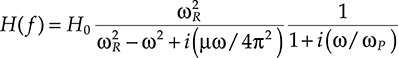
As a matter of fact, from the analysis of a high-confinement VCSEL it is possible to evaluate its response to frequency modulation by obtaining the following approximate equation that is valid for small modulation regimes [19]:
H(f)=H0ω2Rω2R−ω2+i(μω/4π2)11+i(ω/ωP)(5.13)
(5.13)

Figure 5.17 Spectral response to amplitude direct modulation for different values of the bias current of a long-wavelength VCSEL emitting at 1550 nm.
(After Hofmann, W. et al., Uncooled high speed (>11 GHz) 1.55 μm VCSELs for CWDM access networks, Proceedings of European Conference on Optical Communications—ECOC 2006, s.n., Cannes, France, 2006.)
where
ωR is the natural resonance frequency of the VCSEL
μ is the dumping factor of the relaxation oscillations
ωP is a characteristic parameter whose expression can be derived from more fundamental characteristics of the VCSEL and that represents the intrinsic low-pass response of the structure in the absence of laser effect due to parasitic and thermal effects
The frequency response deriving from Equation 5.13 is plotted in Figure 5.17 [19] for an experimental VCSEL emitting at 1550 nm up to 2 mW. The resulting modulation bandwidth is never lower than 10.8 GHz if the bias current is greater than 4.3 mA, qualifying this experimental VCSEL as a very interesting source for high-capacity access networks like G-PON and 10 G-PON and for coarse-wavelength division multiplexing (CWDM) systems.
5.2.4 Tunable Lasers
Almost all semiconductor lasers are tunable by controlling the laser working temperature. Thermal tuning is generally limited to few nanometers, but for devices specifically designed for tuning where it can reach 5–6 nm.
Thermal tuning is generally used to maintain the laser on the correct wavelength through contrasting changes during an operation due to aging and environment.
Another way of tuning a standard semiconductor laser is to change the current injection. As a matter of fact, continuous current injection changes the carrier’s density inside the laser cavity and causes a slight change of the emission wavelength.
Although this second method of tuning is even less effective than thermal tuning it indicates that there are two fundamental ways to tune a semiconductor laser: changing the index through a change in carrier concentration or changing the laser cavity length.
In all the cases, if tuning is achieved by index change, Δλ/λ ∼ r/r; if tuning is achieved by changing the cavity length, Δλ/λ ∼ L/L.
TABLE 5.5 Characteristics of Practical Tunable Lasers for Use as Transmitters in Telecommunication Systems

Network applications involving DWDM systems require a much wider tuning with respect to the potentiality of thermal or current injection tuning in order to use tunable laser effectively.
Generally tuning over an extended C band is required, that is, tuning over 40 nm, while retaining the characteristics of fixed-wavelength lasers.
Today technology offers essentially three types of widely tunable lasers: multisection lasers, external cavity lasers, and laser arrays [1]. In Table 5.5 the main parameters of practical tunable lasers for use as transmitter in telecommunication systems are summarized.
5.2.4.1 Multisection Widely Tunable Lasers
The simpler type of multisection widely tunable laser is a multisection DFB. Since a standard DFB can be tuned thermally only about 5 nm or less, wider tunability is achieved by creating a laser with multiple cavities. Nonuniform excitation along the cavity in DFB laser enables a change in the lasing condition.
Multi-electrode DFB lasers have been realized to achieve nonuniform excitation where the electrode is divided into two or three sections along the cavity [20].
The tuning function is provided by varying the injection current ratio into two sections. A typical geometry for this kind of laser is shown in Figure 5.18.
Tuning in these devices results from the combined effects of shifting the effective Bragg wavelength of the grating in one or several sections and the accompanying change of the optical path length for the change of the refractive index itself.
Combining these effects with thermal discontinuous tuning, a bandwidth on the order of 15 nm can be achieved, which is much more than pure thermal tuning, but it is not enough to cover the entire C band.
Much wider tuning is achieved using multisection DBR lasers.
A principal scheme of a tunable DBR is represented in Figure 5.19 [21]. The central region of the laser is an active region where a heterojunction is realized to allow population inversion and optical gain. The laser cavity is realized by cleaving one of the active region facets and providing, on the other hand, wavelength-selective feedback through a Bragg grating realized in a portion of the laser waveguide external to the active region, called the Bragg grating region.

Figure 5.18 Lateral section of a multisection tunable DFB laser.

Figure 5.19 Lateral section of a multisection tunable DBR laser.
Between the active region and the Bragg grating region there is an intermediate part of the waveguide that is used to adapt the field phase to the cavity length through the change of the refraction index caused by carrier injection. This zone is called phase adaptation zone.
In order to satisfy the resonance requirements, the laser mode has to satisfy the relation
ϕ1−ϕ2=2kπ![]()
where
ϕ1 and ϕ2 are phase change of the Bragg reflector in the active and the phase control regions, respectively
k is an integer
Phase change ϕ2 can be written as
ϕ2=βaLa+βpLp=(2πλ)(raLa+rpLp)(5.14)
![]()
(5.14)
where
subscripts a and p denote the active and phase control regions, respectively
β indicates a propagation constant
λ is the wavelength of the lasing mode
r is the refraction index
The phase ϕ1 accumulated by the lasing mode passing through the Bragg reflector can be derived starting from the properties of Bragg reflectors.
The characteristic parameter γ of the Bragg reflector can be defined, following [22], as
γ2=κ2+(α+iΔβ)2=κ2+[α+2πi(rbλ−12Λ)]2(5.15)
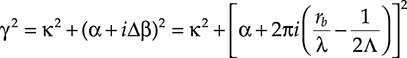
(5.15)
where Λ, κ, α, and rb denote the corrugation period, the corrugation coupling coefficient, the loss of the corrugated region, and the equivalent refractive index for the Bragg reflector, respectively.
The phase change experimented by the field when reflected by the Bragg reflector can be expressed as a function of the characteristic parameter γ and the overall cavity length L as
exp(iϕ1)=−iκrb1γtgh(γL)+(α+iΔβ)=−iκrb1γtgh(γL)+[α+2πi(rb/λ)−(1/2Λ)](5.16)

(5.16)
Substituting Equations 5.14 and 5.15 in Equation 5.16 the relation determining the possible lasing wavelength of the DBR laser can be obtained [1,21].
In particular, the laser will pass from one wavelength to the other when the index of the Bragg reflector section is changed by changing the carrier density with the injection of a current in the area; in general, however, the mode will start free oscillations only if the index of the phase matching section is suitably adjusted to satisfy the phase-matching condition (Equation 5.15).
It is clear that the phase-matching conditions can be attained contemporarily by a set of modes, due to the presence of the addendum 2kπ in the phase-matching condition.
Among the phase-matched modes only one starts laser oscillation: the mode having the highest cavity gain.
The cavity gain of a mode in the DBR structure is given by the gain of the gain section minus the losses in the phase-matching and Bragg sections. But these losses are again controlled by the carrier densities; thus the specific mode to start laser oscillations among those permitted by the phase-matching condition can be selected by correctly polarizing the three laser regions.
The DBR laser is a good tunable laser, but the tuning range is just slightly wider than 5 nm and never exceeds 10 nm, since it is essentially due to the change of the index in the Bragg section (the other indexes are changed to satisfy the phase matching and to select the correct mode, and do not directly contribute to tuning); thus the relationship Δλ/λ ∼ r/r still holds and the limited changing range of the refraction index defines the changing range of the emitted wavelength. It is possible to combine index-driven tuning with thermal tuning and in this way a tuning range as wide as 22 nm has been reached with simple DBR structures.
In order to achieve much wider tuning ranges, the tuning cannot be based only on index changes. Now it is useful to remember that only three causes can generate the tuning of a semiconductor laser structure [23]:
Index changes
Cavity length changes
Mirror wavelength-selective reflectivity tuning
Somehow all these three techniques have to be used if a tuning range twice the DBR maximum of 22 nm has to be reached.
This is possible by using a structure with multiple cavities and a short grating as reflector for each cavity. Sampled-grating DBR (SG-DBR) and super-structure grating DBR (SSG-DBR) lasers implement this idea in two different manners [24].
The sampled-grating design uses two different multielement mirrors to create two reflection combs with different free spectral.
The laser operates at a wavelength where a reflection peak from each mirror coincides. Since the peak spacing is different for various mirrors, only one pair of the peaks can line up at a time, so that, when the lasing wavelength passes from a couple of peaks to the others a big change of emitted wavelength is obtained with a small change of the mirror peak positions (Vernier effect [25]).
The scheme of a discrete tuning SG-DBR and a plot showing the idea of the Vernier effect are shown in Figure 5.20.
Even if this simple explanation of the SG-DBR principle seems to limit this kind of laser to step tuning, a suitable design can achieve also semi-continuous tuning, at the expense of a more complex control algorithm.
Most of the features of the SG-DBR are shared by the SSG-DBR [26] design. In this case, the desired multi-peaked reflection spectrum of each mirror is created by using a phase modulation of grating rather than an amplitude modulation as in the SG-DBR.
Periodic bursts of a grating with chirped periods are typically used. This multielement mirror structure requires a smaller grating depth and can provide an arbitrary mirror peak amplitude distribution if the grating chirping is controlled.
Using SG-DBR or SSG-DBR, discontinuous tuning ranges as wide as 60 nm have been reached, arriving in this way to oversatisfy the requirements.
On the positive side, they are compact, they maintain the properties of fixed-wavelength lasers, and, perhaps more importantly, they are suitable to be integrated with other devices leveraging the InP platform.

Figure 5.20 Lateral section of a multisection sampled grating DBR (SG-DBR) tunable laser. In the lower part of the figure the Vernier effect used to tune the laser by superimposing only one passband of the two gratings that create the laser cavity is also illustrated.
For example, if the output power has to be increased, it is possible to integrate immediately out of the laser, on the same waveguide, a semiconductor optical amplifier to achieve high output power, or if a compact component that can be directly modulated is needed, an InP modulator (either Mach–Zehnder or electro-absorption [EA]) can be integrated at the laser output.
Moreover, the typical reliability of integrated components is higher than that of components composed by different and possibly moving macroscopic parts.
On the negative side, there is the complex electronic control, which is more complex for more performing structures and the difficult processes needed to produce these lasers.
5.2.4.2 External Cavity Lasers
Limitation in tuning range experienced by integrated lasers when tuning is driven by the change of the optical cavity length is due to the fact that in integrated devices this is possible only by injecting carriers and changing the refraction index.
The situation is completely different in external cavity lasers, where the external part of the cavity can change its length with physical means in order to realize sufficient variations for very wide tuning.
The principal scheme of an external cavity laser is shown in Figure 5.21: after reducing the reflectivity of the cleaved active chip facet, part of the emitted radiation is reintroduced in the cavity of an FP semiconductor laser from an external etalon so as to realize a twocavity system: the FP cavity inside the chip and the external cavity.
The effect of the feedback on the original laser emission can be analyzed by introducing two characteristic factors of the external cavity:
The field phase shift Δϕ = ω0τ experienced during a single external cavity round trip, where ω0 is the field angular frequency and τ = 2Lc/c is the cavity round trip, Lc being the cavity length.
The feedback strength κ, defined as the amount of optical power reinjected into the laser.
The feedback strength can be evaluated starting from the reflectivity RE of the external mirror and Rs of the facet of the chip obtaining

Figure 5.21 Schematic view of an external cavity laser.
κ=1−Rsτs√RERs(5.17)

(5.17)
where τs is the laser cavity round trip time.
Naturally the external cavity will influence the laser behavior only if the feedback is not too weak. In order to state a qualitative condition that will help us to understand the order of magnitude of the parameters, let us state that the feedback is relevant for the laser dynamics only if it is more powerful than the spontaneous emission. This seems a reasonable condition since it requires that the feedback be visible by the laser above the noise plateau.
Since in a real laser the reflectivity of the external mirror will be on the order of 0.5 to allow sufficient feedback and sensible output optical power, it can be put at approximately Rs/(1 − Rs) ≈ 1, so that the aforementioned condition becomes
RE≫(Rspτsr)2(5.18)

(5.18)
Equation 5.18 states an important property of external cavity lasers: the shorter the cavity (i.e., the smaller the τs), the more sensitive is the laser to small amounts of feedback. Thus, if the feedback has to strongly influence the laser behavior it needs to design a short cavity laser.
Moreover, it is to be noted that Rsp/r is practically proportional to the laser linewidth Δν (compare Equation 5.8), but for a factor on the order of 1. This factor, due to the condition ≫ appearing in Equation 5.18 can be neglected and the condition can also be written as RE ≫ (Δντs)2 showing that the purer the laser emission (i.e., the smaller the Δν), the more the laser is sensible to reflections.
In order to study an external cavity semiconductor laser, the rate equations have to be written taking into account the electrical field composing the optical wave and not the optical energy, since the feedback has to be represented in terms of the electrical field.
Neglecting the space dependence of the variables and writing the linearly polarized electrical field as E(t) = A(t) exp[iω0t + ϕ(t)], the external cavity rate equations may be written as follows:
ⅆAⅆt=12{g[N(t)−N0]−1τP}A(t)+κτicos[υ(t)]A(t−τ)ⅆϕⅆt=α2{g[N(t)−N0]−1τP}−κτisin[υ(t)]A(t−τ)A(t)ⅆNⅆt=J−N(t)τNA(t)−g[N(t)−N0]A2(t)(5.19)

(5.19)
where τi is the round trip time of the gain chip inside the laser and A′(t) = (κ/τi ) cos[ϑ(t)]A(t − τ) is the intensity of the delayed light injected from the external cavity to the active cavity. The overall ratio between the emitted and the reinjected intensity is indicated by κ and the phase coupling angle is given by the following formula:
υ(t)=ω0τ+ϕ(t)−ϕ(t−τ)(5.20)
![]()
(5.20)
In Equation 5.19 also the noise terms have been neglected, since we are interested in the analysis of the deterministic behavior of the laser.
From the solution of the rate equations the dynamic of the external cavity laser can be studied.
In particular the following property is derived. The laser operation is strongly dependent on the so-called feedback parameter defined as ξ=√(1+α2)κτ![]() , where α is the linewidth enhancement factor of the gain chip.
, where α is the linewidth enhancement factor of the gain chip.
If ξ < 1, the laser is in a regime of weak feedback, the laser cavity coincides with the chip cavity, and the feedback is a perturbation for the laser working. In this regime the rate equations can be solved using the perturbation theory where the “small” parameter is κ.
If ξ < 1 but κ ≪ 0.1, different regimes alternate with stable and unstable regions where, depending on the cavity length and feedback intensity, there is a strong mode hopping or a single-mode operation. However, when single-mode operation is achieved, the laser behavior in this region is quite unstable and changes in environmental parameters or aging can completely change the laser emission.
Moreover, laser tuning is difficult due to this instability. Thus this region is difficult to exploit practically.
If ξ ≫ 1 so that κ > 0.1, a stable operation regime of high injection is reached. The laser cavity is de facto the extended cavity (i.e., the chip plus the external cavity) and the presence of the chip internal facet can be considered a small perturbation to the extended laser working.
In this regime the laser is quite stable, its linewidth is sensibly reduced with respect to the value of the free running chip laser, and tuning can be operated by changing the cavity length without altering laser stability and without provoking mode hopping.
This is the regime in which practical external cavity tunable lasers work.
Considering from now on only the strong feedback regime, the laser output power can be evaluated once the exact laser structure is known. Considering in particular the structure in Figure 5.21, the output power is given by
Po=ηħωɛ(J−Jth)[ln(1/√Rs)αLi+ln(1+/TRsRi)](5.21)

(5.21)
where
η is the chip quantum efficiency
ε is the dielectric constant
Li is the length of the gain chip
T is the total loss internal to the external cavity (e.g., focusing lenses)
Ri is the reflectivity of the cleaved chip facet
The aforementioned equations for power output indicate that, for a given injection current, the external-cavity laser generally has a somewhat lower power output than that of the solitary diode laser and, moreover, has higher threshold current, as shown in Figure 5.22.
As far as tunability is concerned, the emitted frequency is given, with a very good approximation, by the simple equation
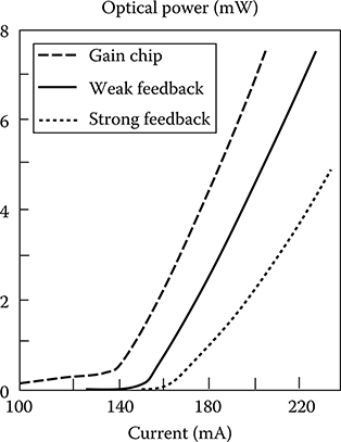
Figure 5.22 Modification of the current optical power characteristic of an FP laser as a consequence of the antireflection coating of a facet and the addition of an external cavity.
ω=2π(Lir+Lcc+k)(5.22)
![]()
(5.22)
where k is an integer. Also in this case, among all the possible oscillating modes, generally only one experiences spontaneous oscillations, that is, the mode having the greater net cavity gain.
Different schemes have been proposed to change the external cavity length, but in practice two have been adopted in commercial products: the use of a wavelength-selective liquid crystal mirror that can be tuned by the applied voltage and a mechanically movable grating mounted on a micromachining electromechanical switch (MEMS) actuator.
In both cases the selectivity of the tunable mirror does not assure stable single-mode operation. On the other hand, a tunable laser for application in DWDM transmission does not need to be continuously tunable; on the contrary it has to be restricted to the International Association for Standardization in Telecommunications (ITU-T) DWDM wavelengths.
Taking into account such a restriction, sufficient wavelength selectivity can be achieved by inserting a solid-state etalon in the laser cavity, whose FSR coincides with the ITU-T grid spacing.
In order to have good control of the optical signal reinjection and to avoid the creation of spurious cavities, special gain chips are produced with a curve-active waveguide, so that the entire cavity appears at the end to be a curve.
The resulting more practical scheme of the external cavity laser is shown in Figure 5.23.
Beside tunability, one of the most interesting features of the high-feedback external-cavity laser is its narrow linewidth. By extending the optical cavity length, the spontaneous recombination phase fluctuation in the laser linewidth can be dramatically reduced. Since resonance oscillations are damped by the small reflectivity of the internal-gain chip facet, the linewidth can be considered Lorentian with an FWHM given by
Δv=ħω0P0gRsp(Δvf)2αt(1+α2)(5.23)
![]()
(5.23)
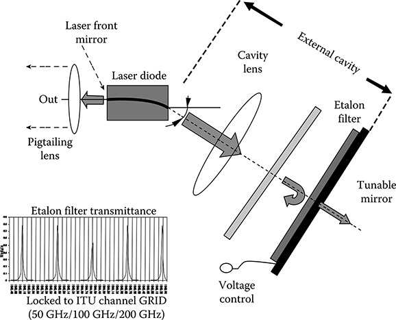
Figure 5.23 Practical implementation of an external cavity laser based on a liquid crystal mirror and on a curved cavity gain chip.
where
P0 is the power in the mode
Rsp is the number of spontaneous emission photons in the mode
g is the local gain
Δvf is the free running linewidth of the gain chip
The linewidth enhancement factor of the gain chip is indicated as usual with α.
The total cavity loss is indicated with αt=a−ln(T2√RsRi)![]() , where a is the optical propagation loss.
, where a is the optical propagation loss.
It is not difficult to derive from Equation 5.23 substituting realistic values to the parameters that the external cavity reduces the linewidth of the gain chip of a factor that can be something like 5 or 7 so that external-cavity lasers with a linewidth of 250 or 500 kHz are used as sources in DWDM systems.
5.2.4.3 Laser Arrays
Laser arrays, where each laser in the array operates at a particular wavelength, are an alternative to tunable lasers. These arrays incorporate a combiner element, which makes it possible to couple the output to a single fiber.
If each laser in the array can be tuned by an amount exceeding the wavelength difference between the array elements, a very wide total tuning range can be achieved.
The DFB laser diode array might be the most promising configuration for wavelength division multiplexing (WDM) optical communication systems due to its stable and highly reliable single-mode operation.

Figure 5.24 Block scheme of a laser array used as a tunable laser.
A possible scheme of a laser array used as tunable laser is sketched in Figure 5.24, where a free space propagation (FSP) region, similar to that used in array waveguides (AWGs), is used to collect the laser output and an SOA to compensate losses.
In principle, this is the easiest way of realizing a tunable laser since it is simply a collection in a single chip of a set of well-known devices: DFB lasers, passive waveguides, an MEMS deflector or an FSP, in case of an output SOA to reinforce the signal.
In practice, the real difficulty consists exactly in creating a chip where all these components are realized together.
In particular, two kinds of implementation problems arise, design and fabrication problems.
From a design point of view, thermal and electrical isolation of all the components is not a trivial problem, since the component footprint has to fit into a standard laser package. Moreover, the design has to be so accurate that all the individual lasers hit the correct wavelength region so that each laser can be tuned on the frequencies for which it is designed by simple thermal tuning.
In case an MEMS deflector is used to focus the light emitted from the laser that is currently switched on onto the output fiber, this element has to be realized with great care for reliability. As a matter of fact, laser interfaces are the elements with a smaller lifetime in a DWDM terminal even when fixed lasers are used. Further shortening of the laser life span is not acceptable from a system point of view.
On the other hand, if an FSP element is used it could be difficult to have a sufficiently high output power without an amplifier at the output of the FSP. In this case, besides the need of a very low-noise and wide-spectrum amplifier, further integration problems could arise.
However, laser arrays have been the first “tunable lasers” to hit the market and they still are a type of tunable lasers widely used in practical systems.
5.3 Semiconductor Amplifiers
Before closing the section on semiconductor lasers a brief presentation of an SOA is needed.
If the reflectivity of the chip facets is eliminated from the structure of an FP laser the chip cannot generate self-oscillation due to lack of feedback, but it can maintain an optical gain due to population inversion in the heterojunction depletion zone.
The result is a traveling-wave semiconductor amplifier.
The dynamics of an SOA is from several points of view similar to that of an ideal amplifier described in Section 4.3.1 with the advantage of having a broad gain curve and a small form factor. Two phenomena limit the use of SOAs in telecommunication systems as signal amplifiers:
As reported in Table 5.1 the typical carrier’s lifetime is on the order of a few nanoseconds, that is, the order of magnitude of the bit time in 10 and 40 Gbit/s transmissions. Thus we have to expect that gain saturation happens during the amplification of signal pulses creating nonlinear pulse distortion as analyzed in Section 4.3.1.3.
The carrier dynamics in a semiconductor creates a link between the phase and the amplitude of the amplifier field so that pure amplitude gain cannot be achieved, but an induced chirp is always present.
Due to these elements the only practical use of SOAs as linear amplifiers is in InP-integrated components where an SOA section is often used to compensate the losses of attenuating components like multiplexers.
The nonlinear dynamics of SOAs is on the contrary an opportunity if they are used not as linear amplifiers but as elements in optical processing circuits.
This is the reason why a more detailed analysis of SOAs, with a particular attention to their nonlinear dynamics, will be delayed up to Chapter 10, where optical signal processing in new-generation networks will be discussed.
5.4 PIN and APD Photodiodes
A photodiode is in general terms a diode whose structure has been designed so as to allow the incoming light beam to reach a zone very near to the p–n junction [27].
If the junction is inversely polarized, all the carriers created by absorbed photons are immediately removed from the junction area due to the inverse polarization field and constitute the photocurrent.
Since the number of generated carriers is proportional to the incoming photon number, the intensity of the photocurrent is proportional to the optical power, so that a photodiode performs quadratic detection of the incoming field.
Since for telecom applications the interesting wavelength region is the near infrared, telecom photodiodes are built using materials with a high-absorption coefficient in this region of the spectrum.
Almost all the photodiodes used in telecom equipments are built using III–V alloy like InGaAsP or InP in order to optimize the absorption in the desired wavelength region [105], but the research on new materials has recently pointed out new alternatives that could give good results in the future [28,29].
Essentially two types of photodiodes are used: PIN photodiodes, where the junction is a p–i–n junction so as to optimize the absorption efficiency, and Avalanche photodiodes (APD), where internal gain is achieved by the avalanche multiplication of the photo-generated carriers.
Considering PIN photodiodes, the first important characteristic is the quantum efficiency η of the photodiode, defined as the probability that an incoming photon will generate a carrier couple that will contribute to the photocurrent.
The expression of the quantum efficiency is given by
η=(1−f)Γ(1−e−αd)(5.24)
![]()
(5.24)
where
f is the facet reflectivity, so that (1 − f) is the probability that the photon is not reflected
α is the absorption coefficient of the junction zone
d is its thickness, so that (1 − e−αd) is the probability that the photon is absorbed in the junction zone creating free carriers
Γ is the probability that the created carrier exits from the junction depletion zone without recombination
From Equation 5.24 the importance of the absorption coefficient is evident and it is this characteristic that selects the photodiode material once the wavelength region is determined.
The photocurrent created by a PIN photodiode as a consequence of the detection of a light beam is composed by four components:
The first term is constituted by the photon-generated carrier flux that is given by cpc = ηqΦ, where q is the electron charge and Φ is the photon flux, that is, the number of photons per unit time arriving on the photodiode front area. It is important to underline that Φ is a random variable, corresponding to the measure of the quantum operator number (nˆ) relative to the incoming field quantum state.
In almost all the telecommunication applications, the incoming field can be considered a time sequence of quasi-stationary coherent states; thus Φ is a Poisson variable whose parameters slowly change as a function, for example, of the field modulation. Assuming a constant incoming field and separating the average and the fluctuations, the photo-generated carrier flux can be written as
cpc=qη〈Φ〉+qη(Φ−〈Φ〉)=RpP+nsh(t)(5.25)
![]()
(5.25)
where P is the power of the incoming optical beam, Rp = q η/ħω is the so-called photodiode responsivity, and the random term nsh(t), which is in all respects a noise term, is the so-called shot noise. The shot noise has a distribution determined by the fact that the photon flux is a Poisson variable and that an incoming photon has a probability η of generating a photocarrier.
Thus, using the probability composition law, the probability distribution of the photocurrent flux can be written as
P(cpcqη=M)=∞Σj=0〈Φ〉e−(Φ)M!(j−M)!ηM(1−η)(j−M)(5.26)
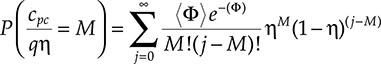
(5.26)
However, if the number of photons arriving on the photodiode in the relevant time unit is much higher than 1, the distribution of the number of photocarriers can be assumed Gaussian, with a standard deviation equal to the incoming optical power.
The second current term is the dark current, which is the current that always pass through an inversely polarized p–i–n junction.
The third term is the current generated by thermally excited carriers and, finally, the fourth is the background noise, which is the current generated by the detection of environmentally generated photons.
Summarizing, the photocurrent is composed of four terms, represented in the following equation:
c(t)=RpP(t)+nsh(t)+ndark(t)+nth(t)+ne(t)(5.27)
![]()
(5.27)
The noise term can be considered in general as Gaussian white noise.
Equation 5.27 holds as far as either the incoming signal bandwidth does not exceed the photodiode bandwidth or the incoming power does not go above the photodiode saturation power.
In the first case, due to the finite time response of the photodiode essentially determined by spurious and junction capacities, the photodiode works as a lowpass filter, cutting too high frequencies.
In the second case, the linear relation between average current and optical power does not hold anymore and the photocurrent tends to saturate, increasing the incoming optical power.
The second type of photodetector is the so-called APD [30].
APDs are high-sensitivity, high-speed semiconductor light sensors. Compared to regular PIN photodiodes, APDs have a depletion junction region where electron multiplication occurs, by application of an external reverse voltage.
The resultant gain in the output signal means that low light levels can be measured and that the photodiode bandwidth is very large. Incident photons create electron–hole pairs in the depletion layer of a photodiode structure and these move toward the respective p–n junctions at a speed of up to 105 m/s, depending on the electric field strength.
If the external bias increases this localized electric field to about 105 V/cm, the carriers in the semiconductor collide with atoms in the crystal lattice with sufficient energy to have a nonnegligible ionization probability. Ionization creates more electron–hole pairs, some of which cause further ionization, giving a resultant gain in the number of electron–holes generated for a single incident photon.
Naturally the avalanche process is not a deterministic one and the generated gain also implies a multiplication noise that adds to the other noise terms typical of a PIN photodiode.
The excess noise is generally represented as a sort of shot noise amplification, so that the expression for the power of the shot noise term has to be modified as follows:
σ2shot=2G2meRpPoFA(5.28)
![]()
(5.28)
where
Gm is the avalanche gain
FA is the excess noise factor, which is a function of the ionization ratio ri, and can be written as [31,32]
FA=riGm+(1−ri)(2−1Gm)(5.29)

(5.29)
Besides multiplication noise, when using an APD, it is to take into account that the dark current noise also is amplified by the avalanche mechanism.
In order to give a correct expression of the amplified dark current noise, one has to take into account that dark current can be divided into two components, depending on the physical phenomenon generating it.
There is a bulk dark current and a surface leakage dark current; the first is really amplified by the APD, and the second does not undergo amplification due to the fact that it is a surface phenomenon.
Thus, indicating with Sbd and Ssd the spectral densities of the two components, the final APD dark current power in the detector bandwidth will be [32]
σ2dc=GmSsdBe+G2mSbdFABe(5.30)
![]()
(5.30)
where Be is the electrical bandwidth of the front end immediately following the photodiode.
5.5 Optical Modulation Devices
5.5.1 Mach–Zehnder Modulators
As we have been discussing the modulation performances of semiconductor lasers at 10 Gbit/s and more it is very difficult to transmit at long distance using laser direct modulation due to the limited modulation bandwidth and to intrinsic chirp associated to it.
Among the external modulators those having better performances, if used in telecommunication equipments, are based on a Mach–Zehnder architecture where the interferometer arms are realized with a material exhibiting a strong electro-optic effect (such as LiNbO3 or the III–V semiconductors such as GaAs and InP) [33,34].
For telecommunication applications, the ones most used are those based on LiNbO3 and on InP.
By applying a voltage on the interferometer branches through suitable electrodes, the optical signal in each path is phase-modulated as the optical path length is altered by the variable microwave electric field.
Injecting an optical field in the interferometer and combining at its output the fields coming from the two branches of the phase modulation it is converted into amplitude modulation due to interference.
If the phase modulation is exactly equal in each path but different in sign, the modulator is chirp-free; this means that the output is only intensity-modulated without incidental phase (or frequency) modulation.
In Figure 5.25 the schematic of a Mach–Zehnder modulator is shown with a particular reference to a LiNbO3 modulator.
Mach–Zehnder modulators can be either dual-drive or single-drive. In a single-drive modulator a single electrode driven by a signal proportional to the data induces phase modulation on one interferometer branch. This phase modulation is designed so that, at the output of the interferometer, the modulated field combines with the unmodulated one either in phase or in quadrature, so as to produce no chirp and the maximum dynamic range in the intensity-modulated optical field.

Figure 5.25 Scheme of a Mach–Zehnder modulator.
The dual-drive configuration uses a data-driven signal on one branch and a signal driven by the inverted data on the other branch to induce modulation on the two branches of the interferometer.
The dual-drive configuration is more stable and resistant to changes in the driving signal and in the environment.
The transfer function of a Mach–Zehnder modulator is shaped as an interferometer characteristic response like 0.5[cos(x) + 1]. This means that the modulator cannot be driven directly with the signal proportional to data, otherwise the nonlinear transfer function will completely distort the signal.
It is needed to bias the modulator with a continuous voltage so as to bring the working point at the center of the linear part of the characteristic, as shown in Figure 5.26. Once correctly biased, the microwave data-carrying signal is correctly modulated onto the optical field.
When digital modulation is adopted, which is almost always, the nonlinear nature of the modulator transfer function is also beneficial, since it helps to eliminate possible overshots in the driving signal.
Due to the need of a bias, every Mach–Zehnder modulator presents two types of electrodes: bias electrodes, to be used for the bias voltage, and signal electrodes, to be used for the data-carrying signal [35].

Figure 5.26 Instantaneous transfer function of a Mach–Zehnder modulator and ideal bias point.
Naturally the instantaneous relation between the modulating and the modulated signals is correct only as far as the signal bandwidth is within the flat frequency response of the modulator.
The modulator frequency response is limited both by the intrinsic bandwidth of the microwave circuit conveying the data and by the spurious capacities embedded in the structure.
Taking as a reference a dual-drive LiNbO3 modulator and assuming an input field perfectly polarized parallel to the modulator waveguide mode, the real modulator response to the optical field is given by [36,37]
H(t)=γLcos[φ1(t)−φ2(t)2]ei(φ1(t)−φ2(t))/2+HXT(t)(5.31)

(5.31)
where
γ is the modulator attenuation
L is the modulator length
φ1(t), φ2(t) are the phase changes on the two arms
HXT(t) represents the interference between the arms
Due to the finite frequency responses h1(t) and h2(t) of the microwave circuit, the phase responses can be written as
φj(t)=φ0+π2∫hj(τ)V(t−τ)Vπⅆτ(j=1,2)(5.32)
![]()
(5.32)
where
φ0 is the bias-induced constant phase that allows to work around the center of the linear part of the cos(x) characteristics
V(t) is the signal carrying the data
Vπ is the voltage that is needed to provoke a phase shift of π/2
hj(t) is the impulse response of the microwave circuit and ideally h1(t) = −h2(t)
From Equation 5.32 it is evident that the frequency response depends, at least in the absence of important defects of the chip, from the microwave circuit conveying the modulating signal.
In Figure 5.27 the frequency response of a dual-drive LiNbO3 modulator is shown whose transfer function is quite flat in a bandwidth compatible with 10 Gbit/s modulation (requiring at least 12 GHz bandwidth due to overhead, see Chapter 3).
A second important effect limiting the response of Mach–Zehnder modulators, especially those built on LiNbO3 for the greater length of the interferometer’s branches, is the different propagation speeds of the microwave and optical fields.
As a matter of fact, this difference creates a misalignment between the modulating function and the carrier to be modulated that depends on the distance along the waveguide, thus inducing signal distortion.
This problem has to be solved with a very careful design of the microwave contacts that convey the microwave signal along the optical waveguide path.

Figure 5.27 Frequency response of a Mach–Zehnder modulator and corresponding response of the microwave circuit conveying the signal.
The design can be conceived in such a way as to use the waveguide contribution to the microwave group velocity to compensate, at least partially, the group velocity mismatch.
Considering overall modulator performances, LiNbO3 modulators have the better characteristics in terms of modulation bandwidth, chirp-free or chirped operation, and dynamic range.
Due to the values of the electro-optic constants of the LiNbO3, modulators built out of this material are bigger than those built out of InP and need much higher microwave voltage.
Performances of InP-based modulators are improving fast and it is possible that in not so long a time the performance difference will almost vanish [38].
At present, LiNbO3 modulators are used in high-quality DWDM interfaces, when compromises are not possible with the signal quality, while InP modulators are used in compact interfaces, like transceivers, where direct laser modulation is not possible. In Table 5.6 the main characteristics of a few practical Mach–Zehnder modulators are summarized.
TABLE 5.6 Characteristics of Practical InP and LiNbO3 Mach–Zehnder Modulators

EOL, end of life value.
5.5.2 electro-Absorption Modulators
EA modulators are based on the change of the absorption coefficient when an electrical field is applied.
This effect is known as quantum-confined Stark effect when happening in quantum well structures, and almost all the practical EA modulators are realized using quantum well structures [31].
The physical description of the effect is quite complex [39], but the final result is that the absorption coefficient, and in particular the absorption edge, that is, the wavelength at which the material lowers abruptly its absorption coefficient and behaves like a transparent material, depends on the applied optical field.
Since the transition between strong absorption and good transparency is quite abrupt and the Stark effect is very fast, this dependence can be used to design a modulator [40].
This effect is shown in Figure 5.28, where the attenuation of a packaged EA modulator is shown at different wavelengths in the fiber third transmission window versus the applied voltage.
The structure of an EA modulator is based on a p–i–n junction built using suitable III–V alloy (e.g., InGaAsP) in order to work at the required frequencies.
Since the modulation mechanism is essentially based on absorption coefficient modulation, the longer the modulator, the greater is the extinction ratio, since the loss in the off state is greater and the signal is better suppressed.
On the other hand, a longer modulator has two issues to solve: the loss is high also in the on state, increasing the modulator insertion loss. Moreover, the longer the modulator, the greater are both the junction and the parasitic capacities, and thus the smaller the modulator bandwidth.
It is clear that there is an unavoidable trade-off between the extinction ratio on the one hand and the insertion loss and bandwidth on the other.

Figure 5.28 Characteristic curve (transmission versus applied voltage) of an EA modulator realized in InGaAsP for different wavelength and polarization of the input carrier.
(After Yamanaka, T. and Yokoyama, K., Design and analysis of low-chirp electroabsorption modulators using bandstructure engineering, 2nd Edn., Second International Workshop on Physics and Modeling of Devices Based on Low-Dimensional Structures, 1998.)
In order to try to remove this limitation, which also constrains the selection of the material with which the modulator is fabricated, traveling-wave EA modulators have been proposed.
Figures 5.29 and 5.30 show the different structures between a lumped and a traveling-wave EA modulator.
In the lump configuration, the microwave signal is applied to the center of the waveguide. At high frequency, due to the strong microwave reflections at both ends, the device speed is strongly dependent on the total resistance capacity (RC) circuit time constant. As shown in the figure, the lumped EA modulator can be modeled as p–i–n junction capacitance Ci and the differential resistance Rd, which represents the resistivity of p- and n-semiconductor materials and metal contact.
In the traveling-wave configuration (Figure 5.30) the device is designed to have microwave co-propagation with optical waves. By matching the output termination, the electro-optic conversion is dominated by the distributed interaction between microwave and optical wave.
The electrical equivalent model of the traveling-wave modulator, as shown in the figure, is a transmission line. The microwave experiences distributed junction capacitance and inductance along the waveguide; thus the limitation is not the total capacitance, but the microwave characteristics, termination and the velocity matching, somehow similar to what happens in the Mach–Zehnder modulator.
Due to the large amount of studies done on Mach–Zehnder modulators and many other microwave circuits, there are several possible solutions to adapt microwave and optical propagation; thus it is possible to design the traveling-wave structure so as to have better performance with respect to the lumped architecture [41].
However, in both the configurations, the more important property of EA modulators is that they can be integrated with other InP-based components.
There are several commercial devices that are built as a laser plus an integrated EA modulator or even a set of DFBs, an EA modulator, and an SOA.
These integrated components are instrumental in the design of small and low-consumption optical interfaces like high-performance XFP transceivers.
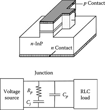
Figure 5.29 Scheme and equivalent circuit of a lumped EA modulator. Rp, junction resistance; Cj, junction capacity; Cp, parasitic capacity.
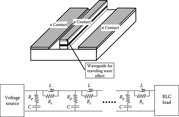
Figure 5.30 Scheme and equivalent circuit of a traveling-wave EA modulator.
(After Zhang, S. Z. et al., IEEE Photon. Technol. Lett., 11(2), 191, 1999.)
EA modulators suitable for modulation up to 40 Gbit/s have been introduced on the market and a summary of the characteristics of practical modulators is reported in Table 5.7.
5.5.3 Integrated Optical Components
It is quite spontaneous to think that, since several optical devices can be fabricated with planar technologies, the evolution of optical devices should somehow repeat the evolution of electronics through multiple function integration and large-scale integration circuits.
In the optical field there are even two possible integration platforms: silicon and III–V alloys, both compatible at first glance with integration of optical devices with electronics.
In practice, there have been several attempts to develop a technology platform for integrated optics and the results of these attempts always have been inferior to expectations.
TABLE 5.7 Characteristics of Practical Lumped and Traveling-Wave EA Modulators

As we will see in Chapter 10 a similar attempt leveraging the III–V platform is ongoing and it is possible that it will have success. But also in this case, the foundation of this possible success will be different from the causes of the success of microelectronics, since it is founded more on the performances allowed by optical integration than on the diffusion of a pervasive generation of low-cost new optical devices.
There are essentially two causes of this evolution: one more fundamental and the other related to the use of optical components.
5.5.3.1 Electrons and Photons in Planar Integrated Circuits
In a CMOS integrated circuit, electrons move into very small wires and experiment several quantum effects due to their associated wave nature, like a tunnel effect.
Consider an electron moving inside the channel of a CMOS transistor at a nonrelativistic energy of 2 eV and with an effective conduction mass of 1.08me, me being the electron rest mass. In these conditions, which are realistic in a standard CMOS working, the electron wavelength is around 6 Å. With this small wavelength it never happens that the electron behaves like a wavelength into the CMOS circuits and the entire design can be performed considering particle properties.
On the contrary, the wavelengths used in optical integrated circuits are generally on the same order or even smaller than the characteristic dimensions of optical integrated circuits.
Thus the photon should always be considered mainly like a wave.
This difference deeply influences the way in which integrated optical and electronic circuits are realized.
The shape of the waveguide core that is used in optical integrated circuits cannot be scaled below a certain dimension, not to risk losing any guiding property.
On the contrary, scaling is always possible with present-day technology in the case of electronics.
5.5.3.2 Digital and Analog Planar Integrated Circuits
Another element that distinguishes planar integration in optics and electronics is the fact that using CMOS circuits it is always possible to realize the required functionalities with a digital circuit, even if they are analogical in nature.
In the optical case, only analogical functionalities exist that have to be integrated together.
It is well known that analog functionalities are much more difficult to insulate in an integrated circuit, especially in a waveguide-based circuit, where the behavior of the photons reflects oscillatory field characteristics.
Just to give an example, it is enough to consider the evanescence-wave directional coupler that is based on the principle that a field can completely pass from one waveguide to another simply because they are near, even without any contact between the waveguide cores.
On the other hand, a sufficiently simple digital optics to push monolithic integration seems faraway, requiring substantial steps ahead before being sufficiently mature for the integration step.
5.5.3.3 Role of Packaging
Unless very high-speed circuits are considered, packaging of very large-scale CMOS circuits is a commodity that can be automated for large volumes through suitable packaging machines.
The situation for optics is completely different at least from two points of view.
The first is related to the way in which the optical field enters into and exits from the package. Unless the component is designed to work in free space, fiber optics is the most natural way to interface the optical chip with the field.
A standard monomode fiber has a core radius around 10 μm, and coupling it with a waveguide is more and more difficult while the waveguide gets smaller and smaller.
In order to achieve a good coupling, either a mode adaptor has to be realized, increasing both the package Bill of Materials and the amount of work to be done serially chip by chip, or complex structures (like multilevel tapers) have to be realized on the planar circuit so that a great part of the circuit area is occupied by coupling structures more than by the component for which the circuit has been realized.
In any case, active alignment is needed in both the cases to arrive at a coupling on the order of magnitude of 3 dB, an operation that is quite expensive.
Besides the coupling problem, high-performance integrated optics has also a temperature stabilization problem.
Both in the III–V platform and in the silicon one, the main materials used to realize planar optical devices are quite sensitive to temperature; moreover, fabrication tolerance creates quite a spread on the characteristics of similar devices (another consequence of the analog nature of optical circuits).
This condition creates the need for a thermal control of the optical components, generally carried out via a Termistor hosted inside the package.
The final effect of these characteristics of optical packaging is that in several cases the cost of the package is higher than the cost of the integrated circuitry inside it. In the case of a DWDM DFB laser, for example, the package and the related elements are worth about 70% of the component Bill of Materials.
5.5.3.4 Integrated Optics Cost Scaling with Volumes
The aforementioned reasons cause the cost model of integrated optics to be similar but not equal to that of microelectronics.
This fact has been studied in particular in the field of optical access regarding the access line home termination. In this field, potential volumes on the order of millions are present on the market, apparently stimulating the development of an integrated optics platform.
The variation of the cost of a component devoted to application in the optical access network is shown in Figure 5.31 versus the volumes for a microelectronic gigabit passive optical network (GPON) processor, an integrated optics GPON interface, and a discrete optics GPON interface. The prices are normalized so as to appreciate better the different trends.

Figure 5.31 Price decrease versus volumes for a microelectronic GPON processor, a discrete optics GPON interface, and a monolithic integrated GPON interface.
From the figure it is evident how the cost of integrated optoelectronic interface scales with volumes a bit faster with respect to the discrete optics components, but quite slowly with respect to microelectronic chips, due to the importance of the package Bill of Materials and the presence of important manufacturing processes serially executed component by component.
5.5.3.5 Integrated Planar III–V Components
Even if in the absence of a radical technology breakthrough there is no possibility to reply with integrated optics the success of microelectronics, it is evident that there are specific situations in which monolithic integration is useful.
The most important is the case of lasers with an integrated modulator (either EA or Mach–Zehnder) and in the case of an output semiconductor optical amplifier.
Devices of this kind are regularly used in telecommunication systems and have the advantage of putting into a single package three elements, sparing on package and connections and reducing interface loss.
This solution is particularly appreciated when a tunable multisection laser is used in conjunction with a Mach–Zehnder modulator.
5.6 Optical Switches
Under the category of optical switches all the optical components can be collected that deflect the light either in free space or in guided propagation from one direction to the other.
In telecommunication, optical switches are used almost only in conjunction with fiber propagation, but for the free space application, which is sometimes used as temporary connection either between nearby units or between parts of a broken cable [42].
Switches used in fiber-optic systems can be classified into two categories: semi-static switches and routing switches.
Semi-static switches are those subsystems that are installed instead of a patch panel to gain flexibility: from a functional point of view they are not routing elements in the network, instead they are part of the cable infrastructure like patch panels, ducts access points, and so on. These switches are generally micromechanical switches and change status quite rarely, sometimes never in their life.
Thus, it is very important that they maintain the characteristics of attenuation and polarization insensitiveness for a long time and that they are able to work after a long time of inactivity.
On the other hand, no important requirements on speed, power consumption, or dimension are generally imposed on these components, but for the fact that without power supply they cannot change state, whatever the state they are occupying (it is said that they have to be latching).
On the contrary, routing switches are designed to provide signal routing, either to find the right path in the network or to protect the signal from a failure.
Here we will talk mainly about routing switches technologies, even if a few of them are applied also to semi-static switches.
There are a plethora of different technologies that have been used to design optical switches, which can be classified as follows [43]:
MEMS: involving arrays of micromirrors that can deflect an optical signal to the appropriate direction
Piezoelectric beam steering involving piezoelectric ceramics providing enhanced optical switching characteristics
Microfluidic methods involving the intersection of two waveguides so that light is deflected from one to the other when a liquid micro-bubble is created
Liquid crystals that rotate polarized light either 0° or 90° depending on the applied electric field to support switching
Thermal methods that vary the index of refraction in one leg of an interferometer to switch the signal on or off
Acousto-optic methods that change the refractive index as a result of strain induced by an acoustic field to deflect light
SOA amplifiers used as gates in an integrated III–V waveguide matrix
Naturally the only way to review in detail all the aforementioned technologies is to devote an entire book to optical switches, and it is not the scope here.
Thus, we will concentrate on a few technologies, those allowing us to better underline achievements and challenges in designing optical switches for telecommunications.
5.6.1 Micromachining Electromechanical Switches (MEMS)
MEMS fabrication techniques utilize the mature fabrication technology of CMOS-integrated circuits (see next section). The fact that silicon is the primary substrate material used in the integrated circuit and that it also exhibits excellent mechanical properties make it the most popular micromachining material.
Limiting our analysis to optical switching applications, there are essentially two techniques that can be used to realize optical switches with silicon-based MEMs: bulk micromachining and surface micromachining [44,45].
Bulk micromachining is the most mature and simple micromachining technology; it involves the removal of silicon from the bulk silicon substrate by etchants. Depending on the type of etchants that are used, etching can be isotropic, that is, oriented along one of the silicon crystal planes, or anisotropic, that is, oriented along a plane different from the crystal main planes.
Anisotropic etching is generally used to expose the silicon crystal planes in order to build mirrors or similar other structures.
Using bulk micromachining the need of complex planar processes is reduced to a minimum, but only the simplest structures can be created.
Surface micromachining is a more advanced fabrication technique. It is based on the use, near the layer of structural materials that are destined to compose the final structure, of layers of sacrificial materials, which are destined to be etched out so as to leave empty spaces between structural layers.
An example is shown in Figure 5.32, which demonstrates how a sacrificial material layer is removed in order to create a suspended mirror.
In addition, from the architecture point of view there are essentially two possible ways of constructing an MEMS optical switch: 2D MEMS and 3D MEMS.

Figure 5.32 Schematic process flow for the creation of a suspended mirror in a planar MEMS. Step 1: sacrifical material deposition; step 2: sacrifical material shaping etchant 1; step 3: structural material deposition; step 4: sacrifical material elimination etchant 2.
In a 2D architecture the movable mirrors are positioned at the intersections of a grid of light paths, either as waveguides or as free space beams as is shown in Figure 5.33. In this case the mirrors act as 2 × 2 switches of a so-called cross-bar matrix (see Section 7.2.1). As an example this can be realized via a mirror that can be lifted and released to deflect or not the light beam, as is shown in Figure 5.34. As evident from the switch architecture, this 2D approach requires N2 mirrors to form an N × N switch. Alternative approaches will be discussed in Section 7.2.1; however, in general, decreasing the number of mirrors causes a more complex interconnection layout that in waveguide circuits is a price that is often hard to pay.
A 3D or analog MEMS has mirrors that can rotate about two axes. Light can be redirected precisely in space to multiple angles—at least as many as the number of inputs.
Since each elementary mirror of this switch has much more than two states, it is expected that a much smaller number of mirrors is needed. As a matter of fact, depending on the exact switch design the number of mirrors varies between N and 2N.
The majority of the commercial 3D MEMS use two sets of N mirrors (total of 2N mirrors) to minimize insertion loss as is shown in Figure 5.35; if only N mirrors were used, the port count will be limited by insertion loss that results from a finite acceptance angle of fibers/lens on the input or on the output side.
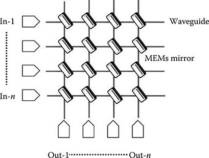
Figure 5.33 Scheme of an MEMS-based cross-bar optical switch.

Figure 5.34 Pictorial representation of an MEMS movable mirror for integration in a cross-bar optical switch.

Figure 5.35 Scheme of a 3D MEMS-based optical switch.
This architecture can be scaled to thousands by thousands of ports with high uniformity in losses. Inevitably the control of the mirrors, being analog and not digital as in the 2D case, is much more complex than in the 2D case and a continuous analog feedback is needed on each mirror to put it in place at the correct angle.
Last thing to consider is the actuating mechanism, which can be either electrostatic or electromagnetic. Electrostatic forces involve the attraction forces of two oppositely charged plates. The key advantage of electrostatic actuation is that it is a very well-consolidated technology, applied in several fields in which MEMS are used like sensors or automotive and very robust and repeatable mechanisms. The disadvantages include nonlinearity in force versus voltage relationship, and requirement of high driving voltages to compensate for the low force potential.
Electromagnetic actuation involves attraction between electromagnets with different polarity. The advantage of electromagnetic actuation is that it requires low driving voltages because it can generate large forces with high linearity. However, the isolation of the different actuators inside the same switch is not easy and it requires a very accurate design.
Since MEMS technology is applied in several fields and MEMS are produced in billions in the world, there are several commercial optical switches based on this technology.
A few reference characteristics are reported in Table 5.8 to get a feeling of what can be done in production devices.
TABLE 5.8 Characteristics of Practical MEMS-Based Optical Switches with Different Architectures

5.6.2 Liquid Crystals Optical Switches
Another consolidated technology that finds application in large areas of the consumer market is that of liquid crystals, which has been used to design optical switches for routing applications [43].
The scheme of Figure 5.36 shows the operational principle of an elementary 2 × 2 liquid crystal switch.
An input polarization diversity system divides the x and y linear polarizations among two branches of the device. On each branch the light passes through a liquid crystal cell and a polarization splitter, which is deflected or not depending on the orientation of the liquid crystal that is fixed by the applied voltage [46].
After the switching the two polarizations are put together again by a polarization splitter.
When liquid crystals started to be used in optical switches their performances were hardly limited by a highly temperature-dependent loss and a very slow switch time. From that date, however, liquid crystal cells have gone several steps ahead and now we can realize cells with a switch time on the order of 300 μs and a loss on the order of 1.2 dB per cell.

Figure 5.36 Scheme of a polarization diversity 2 × 2 optical switch based on two liquid crystal cells (LQ1 and LQ2), each of which work on one of the polarizations (x and y) after their separation via a polarization beam splitter.
These cells also retain the advantage of liquid crystals to consume a low power and to incorporate easily other functionalities inside the switch like broadcasting (obtained by switching polarization of 45°), selective attenuation used to equalize the switch output, and other possible features.
On the other hand, liquid crystal–based devices are necessarily built on micro-optics; thus they scale with difficulty to include thousands of elementary cells, like MEMS do.
For this reason, while liquid crystals are for sure competitive when small switches are considered, it is difficult for large switches to be fabricated with this technology.
5.6.3 Wavelength-Selective Switches
An important application of both LC (liquid crystals) and MEMS is in wavelength selective switches (WSSs), a type of optical switches quite diffused to realize tunable optical add drop multiplexers (OADMs) (see Chapter 7).
The scope of a WSS is essentially to eliminate from the input DWDM comb whatever set of channels is indicated by the network element control.
The functional scheme of a WSS is shown in Figure 5.48: it is essentially a set of components integrating together the demultiplexer and the drop channel separation so that the architecture of the single-side OADM is simplified. The implementation technology is similar to that of 3D MEMs, as shown in Figure 5.37.
In the figure the incoming WDM comb is directed through a discrete 3D optics to a space diffraction grating that divides the different wavelength channels. The channels are successively deflected by the same spherical mirror that has sent them on the grating to a 3D MEMS that directs any channel on the desired direction. In particular, channels to be dropped are sent to one fiber among the array of WSS drop fibers, while channels that are to pass through are sent again on the grating to be multiplexed and deflected toward the output line fiber. This is not the only possible architecture for a WSS, but tunability is generally a characteristic of all WSSs, so that any channel can be send to any drop port.
At the beginning of their introduction there was a lot of suspicion on WSSs due to their characteristics of being completely built through discrete 3D optics: it was believed that they were unstable and unreliable, at least in the long run.

Figure 5.37 Block scheme of a quite diffused WSS architecture.
This prediction, at least up to now, has been demonstrated to be unfounded and WSSs are at present the most affirmed technology for tunable OADMs.
5.7 Electronic Components
When optical transmission was born, in the early 1990s, the industry was completely committed to the development of optical components and there was a diffused idea that optics was going to replace almost completely the electronics in telecommunication equipments.
At present this idea has been demonstrated to be completely incorrect.
Electronic components have evolved so fast in terms of cost and functionalities that electronic signal processing plays a fundamental role in the design of modern transmission systems and switching/routing machines are built using electronic switch fabrics and the situation seems not to change in the medium term.
As a matter of fact, signal processing CMOS circuits based on 45 and 32 nm technology [25] are so fast that real-time signal processing is possible also at the very high-speed characteristics of optical transmission. Thus all the equalization and compensation techniques that have been developed for other applications can now be applied to optical transmission.
As far as switch fabrics are concerned, electronic-based fabrics are convenient both in terms of footprint and of cost, simultaneously offering an unmatched reliability and a great richness of complementary functions.
5.7.1 Development of CMOS Silicon Technology
Beyond any architectural property, a baseline element determining the performance of an electronic equalizer or a switch fabric is the technology with which it is realized.
In this section we will try to understand achievements and challenges for microelectronics when used in telecommunication applications and in particular in electronic equalization of transmission distortions and in switch fabrics.
CMOS circuits are almost the only type of electronic circuits that are used out of analog and special applications.
Their diffusion is due to the combination of very large-scale integration, very low cost, and high performances granted by the great miniaturization.
CMOS require both n and p metal oxide field effect transistors (MOSFETs); hence the name complementary. The base advantage of CMOS versus other types of transistors is that a CMOS circuit only dissipates power when transistors are switched, not when they stay in a definite state, apart from any leakage currents in the system.
Figure 5.38 shows a schematic cross section of a typical advanced CMOS device with low-doped drain contacts implanted through Si3N4 spacers on either side of the gate to reduce the electric field between source and drain.
All gates and ohmic contacts are treated with TiSi2, CoSi2, or NiSi to reduce the resistances of gates and contacts.
The value chain of microelectronics is one of the most complex from wafer vendors to fabrication machine suppliers to foundries and chip producers.
Such a great number of players have to be coordinated to hit common goals and allow an ordinate development of the technology. This is the role of the International Technology Roadmap for Semiconductors (ITRS), an industry road mapping group coordinating the efforts of the players in the microelectronics industry.
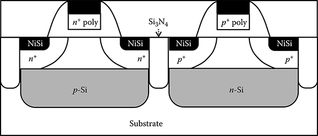
Figure 5.38 Section of an advanced CMOS system.
In order to fix clear targets for the major technology advancement, the ITRS has defined the concept of technology node, the moment at which the entire cycle that is needed to introduce a significant technology improvement through research, experimentation, development, and start of production starts to have an impact on products presented on the market.
Over the last 15 years, there has been a new CMOS technology node approximately every 2 years. The key feature of every node has been a doubling of the density of chips on the wafer and an increase of ∼35% in switching speed and power consumption.
This improvement history is summarized in Figure 5.39 where the sequence of the different technology nodes is shown representing the decrease of the CMOS transistor gate length with time [47,48].
Different reasons have pushed the decrease of the dimensions of the CMOS, all oriented toward the improvement of CMOS circuit performances.

Figure 5.39 Shrink of the characteristic dimensions of CMOS in time and indication of the main technology nodes of the last 10 years.
(After Parthasarathy, S. E. and Thompson, S., Mater. Today, 9(8), 20, 2006.)
The gate length reduction is expected to decrease the time constant associated to the gate of each MOS increasing the circuit speed.
The electronic charge associated to the gate is smaller, thus a switch operation is expected to burn less power.
More circuits fit on the same wafer area, thus a circuit cost is expected to decrease.
5.7.1.1 CMOS Speed Evolution up and beyond the 32 nm Node
As far as the intrinsic RC circuit represented by the transistor gate is dominant over all the spurious RC contributions, the decrease of the gate length is directly related both to the switching speed of the transistor and to the power consumption.
Just to carry out an order of magnitude evaluation, both the capacitance and the equivalent resistance of the CMOS depend on the linear dimensions of the components. Assuming that the material does not change and that all the dimensions but the gate depth scale proportionally (both are in reality not true) in a very first approximation we can write
C=Cp+ɛ0κWLd(5.33)
![]()
(5.33)
R=Rp+ρℓA(5.34)
![]()
(5.34)
where
Cp and Rp are the parasitic capacitance and resistance
ε0 is the dielectric constant of vacuum
κ is the permittivity of the material filling the gate
ρ is the resistivity of the doped silicon electrode
W, L, d are the spatial gate dimensions, d being the depth, ℓ the electrode equivalent length, W the electrode width, and A its equivalent section
If all dimensions scale with the same constant the second term of both Equations 5.33 and 5.34 scale with L, while it is expected that the parasitic term increases, decreasing the characteristic dimensions of the CMOS.
Thus, as far as the parasitic elements can be neglected, it is
B≈1τ≈1(Cp+ɛ0κ(WL/d))(Rp+ρ(ℓ/A))≈1ɛ0ρκdAWLℓ(5.35)

(5.35)
Since the depth of the gate does not scale and A is also proportional to d, the second term of Equation 5.35 would increase almost as the inverse of the square of the gate length.
Unfortunately, the parasitic capacity and resistance cannot be neglected in a high-performance CMOS after the 90 nm node, so that the behavior given by Equation 5.35 is no more even approximated.

Figure 5.40 Intrinsic and parasitic CMOS gate capacitance versus the different component generations.
(After Parthasarathy, S. E. and Thompson, S., Mater. Today, 9(8), 20, 2006.)
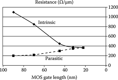
Figure 5.41 Intrinsic and parasitic CMOS gate resistance versus the CMOS generations.
(After Parthasarathy, S.E. and Thompson, S., Mater. Today, 9(8), 20, 2006.)
The decrease of the intrinsic capacitance of the CMOS and the behavior of the parasitic one is demonstrated in Figure 5.40 and a similar plot is shown in Figure 5.41 for the intrinsic resistance and for the parasitic resistance [47].
Several phenomena imply a growth of the parasitic parameters.
As MOSFET geometries shrink, the voltage that can be applied to the gate must be reduced to maintain reliability. To maintain performance, the threshold voltage of the MOSFET has to be reduced as well. As threshold voltage is reduced, the transistor cannot be switched from complete turn-off to complete turn-on with the limited voltage swing available.
The final MOS design is a compromise between strong current in the “on” case and low current in the “off” case. Sub-threshold leakage which was ignored in the past can now consume upward of half of the total power consumption of modern high-performance very large-scale integration (VLSI) chips [49,50].
The gate oxide, which serves as insulator between the gate and the channel, should be made as thin as possible to increase the channel conductivity and performance when the transistor is on and to reduce subthreshold leakage when the transistor is off.
However, with current gate oxides with a thickness of around 1.2 nm (which in silicon is ∼5 atoms thick) the quantum mechanical phenomenon of electron tunneling occurs between the gate and the channel, leading to increased power consumption.
Insulators (referred to as high-k dielectrics) that have a larger dielectric constant than silicon dioxide, such as group IV metal silicates, for example, hafnium and zirconium silicates and oxides, are being used to reduce the gate leakage from the 45 nm technology node onward. Increasing the dielectric constant of the gate insulator allows a thicker layer while maintaining a high capacitance (capacitance is proportional to dielectric constant and inversely proportional to dielectric thickness).
To make devices smaller, junction design has become more complex, leading to higher doping levels, shallower junctions, and so forth, all to decrease draininduced barrier lowering. To keep these complex junctions in place, the annealing steps formerly used to remove damage and electrically active defects must be curtailed [51], increasing junction leakage. Heavier doping is also associated with thinner depletion layers and more recombination centers that result in increased leakage current, even without lattice damage.
Traditionally, switching time was roughly proportional to the gate capacitance. However, with transistors becoming smaller and more transistors being placed on the chip, interconnect capacitance (the capacitance of the wires connecting different parts of the chip) is becoming a large percentage of capacitance [50]. Signals have to travel through the interconnect, which leads to increased delay and lower performance.
Figures 5.40 and 5.41 individuate a threshold technology node with a dimension of the gate on the order of 22 nm, where the parasitic resistance and capacitance will become almost equal to the intrinsic one.
Before that point, the strategy to decrease the dimensions is effective in increasing the CMOS switching speed; beyond that point, it seems to become less and less effective up to a point at which the component will become slower while shrinking.
This evolution is individuated also in Figure 5.42, where the inverse of the response time is plotted versus the technology node.

Figure 5.42 Impact of parasitic capacitance and resistance on CMOS commutation speed.
(After Parthasarathy, S.E. and Thompson, S., Mater. Today, 9(8), 20, 2006.)
TABLE 5.9 Characteristic Speed and Power Consumption of 65 nm Gate CMOS Elements Optimized for Different Applications
TPD (ns) |
Total Power Consumption at Maximum Speed (μW) |
|
Standard gate |
75 |
750 |
High speed |
0.9 |
760 |
Advanced |
0.5 |
738 |
Low voltage |
9 |
720 |
To manage the increase in parasitic Rp and Cp a number of solutions are under consideration, among them using novel silicides different from Si3N4 and reduced polysilicon height [10] that will bring to a vertical the scaling of the structure.
Another option is that along critical paths of a circuit, the devices are not placed as close as possible to the nearby devices in the wafer. In this case there is some area penalty, but there may be a path for reducing the device degradation caused by the nominal device pitch.
Concluding the section on CMOS switching speed, Table 5.9 provides figures for last-generation CMOS gates in terms of characteristic propagation time [52,53]. This is expressed through the propagation delay, which is the time for an input instantaneous switch to manifest at the gate output.
Considering the digital circuits speed, last generation CMOS are currently used to design processors and other digital circuits dedicated to very high volume markets with a clock up to 20 GHz, while special applications ASICS have been developed up to a clock as high as 50 GHz, reached not only via the choice of the most advanced transistor, but also through a careful circuit design that uses all the structures needed to achieve a so high speed.
So high speed CMOS can be used, and in practice have been used, to design also analog microwave circuits, having performances that are comparable with the more traditional III–V transistors used in these applications.
Analog microwave circuits have been realized with 45 nm and 32 nm CMOS having a passband as high as 50–60 GHz confirming the exceptional speed of these components.
5.7.1.2 CMOS Single-Switch Power Consumption
An ideal CMOS dissipates power only when switching from one state to the other. In reality, the presence of a leakage current, due to several reasons, induces a power consumption also in steady state.
As far as the switching power consumption is concerned, it is related to the dissipation of the electron charge accumulated into the dielectric part of the charged MOS.
Thus the power consumption during switching depends on the switching frequency (number of switching operations per second) and on the dimensions of the gate.
It is interesting to analyze the power consumption at the maximum switching speed, for which indicative values are reported in Table 5.9.
When the CMOS is used to build a switch fabric it is interesting to analyze the energy needed to switch an elementary CMOS gate.

Figure 5.43 Realization of a 2 × 2 switch with logical CMOS gates.
A simple digital 2 × 2 switch can be constructed as a circuit with three inputs and two outputs: the three inputs are the two signals and the control; if the control is on the switch is in the bar state, if the control is off the switch is in the cross state (see Figure 5.43). Realizing the circuit with simple gates and counting the number of elementary CMOS it is possible to evaluate the power consumption per bit of the switch.
Assuming a clock at 3 Gbit/s and a total power consumption of 750 μW, we obtained a value of 3 pJ/bit for the energy consumption per bit.
As underlined in the caption of Table 5.9, data we are using are relative to the 65 nm technology node since this component generation is widely diffused in high-volume products and reliable average data are available.
It is possible to imagine that passing to 35 and 22 nm the power consumption will further decrease and it will be possible to get near the value of 1 pJ/bit, which is considered the target for the consumption of electronic switches.
5.7.1.3 CMOS Circuit Cost Trends
A powerful driver both for the shrink of CMOS dimensions and for the increase of wafer radius is the continuous push to decrease prices of CMOS circuits even if functionalities grow.
The price to pay for this evolution is the use of more and more expensive planar processes, whose cost is partially due to the requirement to fabricate smaller and smaller structures and partly to the need of maintaining the process uniformity over greater and greater wafers.
This evolution is represented in Figure 5.44, where the time evolution of the cost in dollars of a single CMOS (estimated starting from the average cost of an integrated circuit) is compared with the time evolution of the cost of a lithography machine [47].
The cost of the CMOS is decreased as much as seven orders of magnitude, even if the lithography tooling has become continuously more expensive.
At the end of the story, this is really the propulsive strength of microelectronics: it is able to conjugate better performances and lower prices.
Before illustrating specific telecommunication applications of electronics, we will briefly illustrate the structure and the performances of three base electronics-integrated circuits: the application-specific integrated circuit (ASIC), the field-programmable gate array (FPGA), and the digital signal processor (DSP). The evolution of these circuits is not mainly driven by telecommunications, since they find application in a much wider market, comprising consumer appliances and almost all the industrial machinery.

Figure 5.44 Trend of the CMOS cost and of the cost of the lithography tooling.
(After Parthasarathy, S.E. and Thompson, S., Mater. Today, 9(8), 20, 2006.)
It is a fact, however, that the continuous enhancement in the capabilities of such circuits has conditioned strongly the design of telecommunication equipments. Electronic equalization would not be possible without suitable DSPs and FPGAs, while the evolution of router capacity has been strongly driven by the evolution of the ASIC performances.
ASICs and FPGAs have been largely used to fasten the complex functionalities of next-generation SDH/SONET ADMs and of Carrier Class Ethernet switches, up to the level that the design of an interface card of a packet machine (would be a router or a switch) partially coincides with the design of ASICs or with a programming of FPGAs with suitable characteristics.
5.7.2 Application-Specific Integrated Circuits
ASICs are, as the name indicates, nonstandard integrated circuits that have been designed for a specific use or application. Generally an ASIC design will be undertaken for a product that will have a large production run, and the ASIC may contain a very large part of the electronics needed on a single integrated circuit.
Despite the cost of an ASIC design, ASICs can be very cost-effective for many applications. It is possible to tailor the ASIC design to meet the exact requirement for the product and using an ASIC can mean that much of the overall design can be contained in one integrated circuit and the number of additional components can be significantly reduced.
This is why ASICs have such a big success in the line cards of large switching machines. These are quite complex subsystems, including a large processing capacity besides the physical interface with the transmission systems and besides memories, and all that is needed to complement a fast dedicated processor.
In Chapter 7 we will see that complex operations in a switching machine are carried out directly in the line card, such as QoS management.
Concentrating a large number of functionalities in a single ASIC is in these cases a key tool to ease the design and maintain, despite the complexity, high performances.
The development and manufacture of an ASIC design including the ASIC layout is a very expensive process. In order to reduce the costs, there are different levels of customization that can be used. These can enable costs to be reduced for designs where large levels of customization of the ASIC are not required. Essentially there are three levels of ASIC that can be used [54]:
Gate array: This type of ASIC is the least customizable. Here the silicon layers are standard but the metallization layers allowing the interconnections between different areas on the chip are customizable. This type of ASIC is ideal where a large number of standard functions are required which can be connected in a particular manner to meet the given requirement.
Standard cell: For this type of ASIC, the mask is a custom design, but the silicon is made up from library components. This gives a high degree of flexibility, provided that standard functions are able to meet the requirements.
Full custom design: This type of ASIC is the most flexible because it involves the design of the ASIC down to transistor level. The ASIC layout can be tailored to the exact requirements of the circuit. While it gives the highest degree of flexibility, the costs are much higher and it takes much longer to develop. The risks are also higher as the whole design is untested and not built up from library elements that have been used before.
In any case, the ASIC design is a complex task and several studies have been carried out on the process for ASIC design and on the ways to decrease the risk.
As far as the performances are concerned, a good design allows an ASIC to have a better possible performance for the specified task, due to its specialization.
Still at 90 nm, ASICs with a clock rate on the order of 20 GHz were produced for a variety of applications [55] and this limit decreases continuously, up to the ASICs with a clock rate exceeding 50 GHz that were produced using 45 nm technology [56].
It is to be expected that 32 and 22 nm ASICs will be still faster, and it is not unbelievable that 22 nm ICs will reach 80 GHz clock, which is a threshold for some telecommunication functionalities, like nonlinear equalization for 100 Gbit/s multilevel transmission (see Chapter 9).
As far as the throughput is concerned, experimental ASICs for security applications have been constructed with a single line serial throughput as high as 61 Gbit/s for an aggregate throughput on two parallel ports in excess of 121 GHz [57].
Another key feature of ASICs is the maximum area available. As a matter of fact, this is directly related to the number of transistors that can be integrated and thus with how functional each of the ASICs can be.
Measuring the ASIC area in a number of equivalent gates, ASICs with an area of more than 105 equivalent gates have been already built and this number will continuously increase while 32 nm technology will become more consolidated and the gates and functional libraries will enlarge, allowing easier ASICs design. It is to be taken into account that high-performance 45 nm ASICs are in production with an equivalent area of more than 7 × 10⁵ gates [58]; thus it is expected that 32 and 22 nm technology will do better due both to smaller CMOS and to the continuous effort to increase the process planar uniformity.
5.7.3 Field Programmable Gate Array
FPGA chips are the most powerful and versatile programmable logic devices. They combine the idea of programmability and the architecture of uncommitted gate array which is one of the ways to develop ASICs [59].
The main elements of an FPGA chip are a matrix of programmable logic blocks (these blocks are named differently, depending upon a vendor) and a programmable routing matrix.
The interconnections consist of electrically programmable switches which is why FPGA differs from Custom ICs (see Section 5.7.2), as these are programmed using integrated circuit fabrication technology to form metal interconnections between logic blocks (see Section 5.7.2).
An abstract FPGA block scheme is shown in Figure 5.45, where these fundamental building blocks are shown in a common FPGA architecture, in which the logic blocks are arranged as a square matrix. However, different vendors use different internal architectures, functional to their particular logic block and routing technology and to the performances [60].
FPGA configuration memory is usually based on volatile SRAM (static random access memory), so these FPGAs must be connected to a dedicated Flash chip if stable memory has to be implemented. However, there are also both SRAM-based FPGAs with integrated flash module and pure Flash-based FPGAs that don’t use SRAM at all.
5.7.3.1 Programmable Connection Network
In order to build the programmable connection network, present-day FPGAs adopt essentially two different technologies: SRAM-controlled switches and antifuse.
An example of the use of an SRAM-controlled switch is shown in Figure 5.46 where the connection between two logic blocks through two switches constituted by one pass transistor and then a multiplexer is depicted. The whole subsystem is controlled by SRAM cells [61].
Figure 5.45 Functional block scheme of an FPGA.
Figure 5.46 Example of interconnection between two logic blocks within the reconfigurable network inside an FPGA based on elementary switches and SRAM controllers.
(After Actel, Technical Reference for Actel Antifuse FPGAS, 2010, www.Actel.com [accessed: October 18, 2010].)
The other type of programmable switch used in FPGAs is the antifuse. Antifuses are originally open circuits and take on low resistance only when programmed. Antifuses are suitable for FPGAs because they can be built using modified CMOS technology [62].
Generally antifuses rely on saturable insulators, that is, materials that have a very high resistance without an applied voltage or if the voltage is below a threshold, but if the voltage is brought above the threshold abruptly, the resistance goes down to values typical of a conductor.
Amorphous silicon has a similar behavior and is effectively used in a few antifuses, but much more specialized materials exist that are compatible with the CMOS technology.
5.7.3.2 Logic Block
Logic blocks of an FPGA can be constituted by a large variety of sub-circuits, depending on the use for which the FPGA is designed.
Logic blocks simply as a couple of transistors or a flip-flop are used in some FPGAs, like in other complex structures using a look-up table and a set of logic ports are adopted.
An example of a complex-structure logic block is shown in Figure 5.47 [61]. Such a logic block includes look-up tables and two flip-flops, besides a certain number of logical gates.
Logic blocks of this type are also called configurable, since their functionality can be configured through the content of the look-up tables.
5.7.3.3 FPGA Performances
Since FPGAs are modular elements whose inner connectivity depends on the task to be realized; the performances of these elements depends both on the particular FPGA inner architecture and on the type of function to be carried out.
In telecommunication applications FPGAs are used, for example, to implement digital signal processing in equalization engines, to manage header information in simple communication systems or to carry out protocols in switching machines.

Figure 5.47 Example of reconfigurable logical block of a high-performance FPGA.
(After Actel, Technical Reference for Actel Antifuse FPGAs, 2010, www.Actel.com [accessed: October 18, 2010].)
We will select a particular application that is quite studied in literature and that is a key for several equalization algorithms: basic linear algebra subroutines (BLAS).
We will essentially follow [63] in comparing the performances of a typical high-performance FPGA with C programs to execute linear algebra operations with both a standard high-speed central processing unit (CPU), and with a massively parallel graphic processing unit (GPU) running a standard mathematic kernel for high-performance and high-precision applications.
The time elapsed to perform a standard operation on an N × M matrix (like the multiplication for a 1 × M vector) is shown in Figure 5.48. The disadvantage of the FPGA versus a fast CPU with an advanced mathematical kernel is not so significant, and even the parallel GPU with the mathematical kernel gains only about a factor of 3 in speed, at the cost of an expensive and complex parallel processor.
Moreover, a correctly programmed FPGA is superior to a standard C programming of about a factor of 1.8, qualifying as a real-time processor.
On the other hand, the FPGA advantages are clear in terms of dissipated power, which is one of the main parameters to judge the electronic circuitry for signal processing.
In all the considered examples the FPGA is able to go over the 3000 iteration per Joule of burned energy, while the GPU can carry out an average number of 800 iterations for burned Joule and the CPU less than 600.
This is an important advantage that qualifies FPGA as a competitive alternative for many telecommunication applications, where the consumed power is a key issue.
Another useful comparison is between FPGAs and ASICs. In this field it is clear that the FPA will always have worse performances due to the specific optimization of a well-designed ASIC. On the other hand, carrying out an FPGA project can be 10 times less expensive with respect to an ASIC project and the final ASIC, once in production, has a competitive price only if produced in very large volumes, which is not the case generally for telecommunications.

Figure 5.48 Example of performance evaluation of a programmed FPGA in the task of executing linear operations on arrays and vectors. (After Kestur, S. et al., BLAS comparison on FPGA, CPU and GPU [a cura di], IEEE Computer Society, Annual Symposium on VLSI (ISVLSI), 2010, IEEE, s.l., pp. 288–293, 2010.)
This consideration often leads designers to use FPGAs instead of ASICS every time the required performances allow it.
5.7.4 Digital Signal Processor
A DSP is a particular type of CPU optimized to run real-time digital processing algorithms like fast Fourier transform (FFT), digital filtering, digital correlation, and so on.
In order to do that, a DSP is realized with a set of hardware-implemented functions that are suitable for the target of the processor, while generally the configuration interfaces are not so powerful as those of a standard CPU, since a DSP is not built to change continuously the program in order to carry out a large variety of tasks (as a standard computer does), but to execute on a high-speed transit signal a well-defined set of operations that perhaps will be programmed at the beginning of the DSP’s life and will never change.
Due to their design target, DSPs are used almost always as local controllers or equalizers, and the telecommunication application is not an exception.
For convenience, DSP processors can be divided into two broad categories:
General-purpose DSP processors: These are basically high-speed microprocessors with hardware and instruction sets optimized for DSP operations.
Special-purpose DSP processors: These include both hardware designed for efficient execution of specific DSP algorithms like FFT or feed-forward equalizer (FFE)–decision feedback equalizer (DFE) filtering and hardware designed for specific applications like forward error correction (FEC) coding–decoding.
5.7.4.1 DSP Hardware Architecture
In most of the applications requiring the use of a DSP, digital algorithms like digital filtering and FFT involve repetitive arithmetic operations such as multiplication, additions, memory access, and heavy data flow through the CPU.
The Von Newman architecture of standard microprocessors is not suited to this type of activity due to the fact that heavy mathematics without any access to the memory or to the input/output interfaces of the system practically nullify the ability of the processor to share the computation power among different processes exploiting the time each process takes to access the memory or the peripheral devices of the system.
DSPs overcome this difficulty by a hardware architecture that exploits a sufficient degree of parallelism so as to avoid the intense mathematics that will destroy the processor performance.
An example of basic DSP architecture is shown in Figure 5.49; this is a particular implementation of the so-called Harvard architecture [64] and exploits different levels of parallelism to speed the real-time processor operations:
Program memory is separated by the data memory, thus massive data transfer does not collapse the transfer of program instructions to the arithmetic–logical unit (ALU). Moreover, in a standard microprocessor, where the program codes and the data are held in one memory space, the fetching of the next instruction while the current one is executing is not allowed, because the fetch and execution phases each require memory access. On the other hand, since the execution of an instruction requires fetching and decoding before the effective execution phase, it would contribute to speed up operations if the fetching phase would be carried out contemporary to the execution of a previous instruction. This is possible if data memory and program memory are separated and exploit separate busses. Thus, in a DSP with the architecture of Figure 5.49 two instructions are contemporary under processing in the ALU, one is executed, the other fetched. In many DSPs the pipeline process, which is the process constituted by putting in parallel different operations with a different state of completion, is even more developed. In these cases, three instructions are active at the same time: one is in the fetching state, the second in the decoding state, and the third in the execution state.

Figure 5.49 Architecture of a basic DSP.
The data memory is separated into two independent memory units, each of which has its own bus; in this way parallel data transfer is possible, easing operation on real-time data coming from the environment, for example, on data arriving from a transmission line.
The ALU is supported by the parallel operation of a multiplier with an accumulator. The basic numerical operations in DSP are multiplication and addition. Multiplication in software is time-consuming, and additions are even worse if floating-point arithmetic is used.
To make real-time DSPs possible, a fast dedicated hardware Multiplicator and Accumulator Circuit (MAC), using either fixed-point or floating-point arithmetic, is mandatory.
This device also generally uses a pipeline process, since the operations can be represented in three steps: data read, execution and accumulation. Thus generally also the MAC has three active, contemporary operations, each of which is in a different state of its life cycle in the MAC.
The ALU is also supported by a shifter that allows recurring operations to be carried out efficiently.
Beyond the basic architecture of Figure 5.49, a much higher degree of parallelization can be realized in high-performance DSPs, as shown in Figure 5.50. This architecture is inspired by what is presented in [65]; however, it is not intended to be the real product architecture, as it is simplified and schematized for explanation purposes and to present a more general example. Here, up to four MACs can be put in parallel to support the ALU in executing recurrent operations. The MACs are not connected to the ALU via the program bus, but via dedicated connections that allow a much more effective pipelining.
Moreover, different DSPs can be built, where one or two MACs can be substituted by other kinds of support units that operate in parallel, like shifter or more complex logical units that can perform also complex operations using hardware-coded instructions.
The pipeline operation and the division of the computation load among the ALU and the other parallel processing units are cared for by a specific part of the chip, a program control unit. This is supported by a sequencer that constructs the sequence of instructions for each parallel element.
The program control unit has also as support an emulation unit that allows more complex operations that have to be emulated via the inner language of the machine to be solved without charging the ALU. As a matter of fact, emulation is a complex operation that would slow the pipeline operation if it would be in charge of the ALU.
Finally different input/output units exist for data and program that are not shown in the figure.
5.7.4.2 DSP-Embedded Instruction Set
Besides architecture that facilitates intense real-time mathematics, the DSPs are equipped with an internal set of machine language instructions that are very different from those of general-purpose CPUs.
Figure 5.50 Architecture of a more advanced DSP.
(After Ceva, The Architecture of Ceva DSPs—Product Note, 2010, www.ceva-dsp.com [accessed: October 18, 2010].)
As a matter of fact, depending on the DSP-specific architecture, several recurring operations in digital processing are carried out by hardware parts of the ALU or by parallel elaboration circuitry, like MACs.
For example, key parts of an FFT algorithm can be encoded into a single machine language instruction in a DSP optimized for this kind of application.
Moreover, a DSP-embedded instruction set is almost always a reduced instruction set computer (RISC) set, where no micro-language is present to elaborate complex instructions.
The characteristics of a RISC set are as follows:
The instructions are short and the execution time does not vary so much from instruction to instruction.
The instructions have a fixed length.
Every instruction is executed in a clock cycle.
Memory is addressed with a small number of simple instructions.
In order to face the reduced number of instructions and the absence of micro-language, registries are used much more than in a traditional CPU.
Pipelining is easier.
5.7.4.3 DSP Performances
As in the case of FPGAs, it makes little sense to talk in detail about DSP performances, as they vary depending on the application and on the inner DSP architecture.
In the following part of this chapter we will see a lot of applications requiring DSPs or FPGAs in order to have an idea of what can be achieved with these electronic circuits in the telecommunication environment.
5.8 Electronics for Transmission and Routing
After a general review of the developments of microelectronics and of the architecture of a few general-purpose circuits that have a relevant impact on telecommunication systems, we discuss in this section a set of specific applications of microelectronics to telecommunication equipments.
Naturally these are only a subset of the use of ICs in telecommunications and cover a set of recent evolutions both in transmission system performance enhancement and in the solution of the addressing problem in switches and routers, which has been for a long time the bottleneck of the performances of such machines.
There are a lot of other applications of microelectronics, like integrated switches and single cross-point implementation, control processors for element and network management and CPUs for protocol running.
A few of these applications are in the field of general-purpose electronic systems, like the control board of the telecommunication equipments; others are consolidated technology, even if the continuous CMOS platform development leads to a continuous performance enhancement.
However, the field of electronics application is so large that for sure it can happen that the reader is interested in something that is not even cited here. More specific books on electronics for telecommunications surely will help the interested reader to go more in deep in this subject. [64,66,67].
5.8.1 Low-Noise Receiver Front End
Before reviewing digital signal processing applied to optical transmission, we will consider an important analog device that is present in all transmission systems: the low-noise amplifier that has the role of amplifying the photocurrent coming out from the photodiode up to a level suitable to be processed by the electronic receiver [32,68,69].
This amplifier noise characteristic determine almost completely the thermal noise performances of the receiver, since it is the first element of the electronic amplifier chain.
In order to have a low noise figure, the input impedance of the amplifier has to be high, so a high-impedance amplifier is suitable for this application.
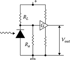
Figure 5.51 Electrical scheme of a high-impedance receiver front end.
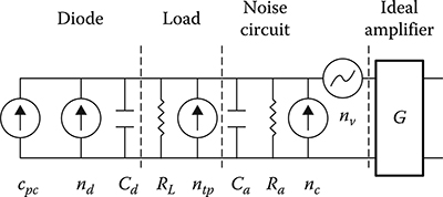
Figure 5.52 Equivalent circuit of a high-impedance receiver front end.
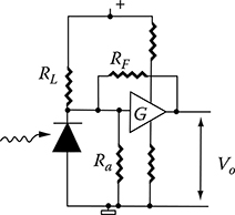
Figure 5.53 Electrical scheme of a transimpedance receiver front end.
The scheme of a high-impedance amplifier following a photodiode is plotted in Figure 5.51, while its equivalent noise circuit is shown in Figures 5.52 and 5.53.
In the equivalent circuit, the photodiode is represented as a capacitor in parallel with the photocurrent generator and the dark current generator while the amplifier is divided into three sections: the load resistance, the noise circuit representing the thermal noise contribution, and an ideal amplifier providing the gain G and the lowpass characteristics with a bandwidth equal to Be.
This structure is aimed to minimize the noise contribution with a very high input resistance. This design implies a small passband and in order to achieve a large electronic bandwidth the amplifier has to be accompanied by an equalizer.
From the equivalent circuit it is clear that the noise results from two main sources: the photodiode noise, which can be modeled as a noise current, and the amplifier noise process, which can be modeled as a current noise and a voltage noise.
Thus the overall circuit noise can be modeled as follows:
nt(t)=G[ntp(t)+nc(t)+ncv(t)](5.36)
![]()
(5.36)
where the noise contributions are defined in Figure 5.51 and ncv(t) is the noise current generated by the voltage noise at the amplifier input.
The power of the photodiode thermal noise can be written as
σ2tp=4kBℑRLBe(5.37)
![]()
(5.37)
where
kB is the Boltzmann constant
ℑ is the absolute temperature
RL represents the photodiode load resistance
The power of the process ncv(t) can be evaluated by evaluating the input admittance of the amplifier. In particular, calling the admittance Y(ω), the power spectral density of the voltage process nv(t) with Sv(ω) and the ideal amplifier transfer function HG(ω), we obtain
σ2cv=∫|Υ(ω)|2|HG(ω)|2Sv(ω)ⅆω≈Sv[BR2in+43π2(Ca+Cd)2B3](5.38)

(5.38)
Combining Equations 5.36 with 5.37 and 5.38, the overall power of the thermal noise at the receiver is given by
σ2th=G2{4kBℑRLBe+ScBe+Sv[BeR2in+43π2(Ca+Cd)2B3e]}=Fa4kBℑRLBe(5.39)

(5.39)
where the noise factor of the receiver Fa is given by
Fa=G2+G2ScRL4kBℑ+G2RLSv4kBℑ[1R2in+43π2(Ca+Cd)2B2e](5.40)

(5.40)
From Equation 5.39 it results that the minimum noise is achieved by increasing RL as much as possible. The limit to the increase of RL is given by the bandwidth of the front end which is approximately proportional to 1/RL. Even if an equalizer is used to improve the bandwidth, the relationship between noise and bandwidth constrain the design of low-noise high-impedance front ends.
This limitation can be overcome by means of the so-called transimpedance front end, whose scheme is shown in Figures 5.52 and 5.53 while the equivalent circuit is sketched in Figure 5.54.
The transimpedance of the front end is defined as the ratio between the amplifier input current (that is the photocurrent) and the output voltage and can be written as
ZG(ω)=RF1+(1/G)+(RF/RLG)+(iωCinRF/G)(5.41)
![]()
(5.41)
If the circuit after the front end read the voltage at the front end output as a useful signal, the bandwidth of the front end can be written as
Be=G2πRF(Ca+Cd)(5.42)
![]()
(5.42)
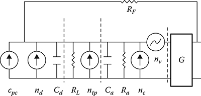
Figure 5.54 Equivalent circuit of a transimpedance receiver front end.
while the noise at the amplifier output can be evaluated with a procedure similar to that carried out for the high-impedance front end, obtaining
σ2th=G2{4kBℑRFBe+ScBe+Sv[BeR2F+43π2(Ca+Cd)2B3e]}=Fa4kBℑRLBe(5.43)

(5.43)
The principle on which the transimpedance amplifier is based is clear from Equations 5.42 and 5.43: the noise is limited by the high feedback resistance while the bandwidth can be wide if the open loop gain is sufficiently high.
5.8.2 Distortion Compensation Filters
During propagation through an optical fiber the signal undergoes both linear and nonlinear distortion and the performance of an optical transmission system largely depends on how these distortions are managed.
The main deterministic linear distortion is chromatic dispersion and dispersion compensation is mandatory in high-performance transmission systems.
If dispersion is optically compensated, through a distortion compensation filter (DCF), for example, it is possible to compensate many wavelength channels together; moreover, since optical compensation is applied before the receiver, the only nonlinearities that are present are those related to fiber propagation, which generally can be considered small. Thus in a first approximation optical dispersion compensation can work on a linear channel.
On the other hand, if dispersion is to be compensated after the detection via an electronic circuit, one compensator per channel is needed; moreover, the photodiode square detection law creates a strong nonlinearity in the channel before the electronic compensator.
Nevertheless, electronic dispersion compensation has several attractive characteristics, so that it is nowadays almost always present in high-performance systems.
The cost of electronic circuits is not so high, so that from a cost point of view, having one compensator for each channel is not a big problem. On the other hand, per channel compensation allows accurate management of the dispersion slope and of the polarization mode dispersion (PMD), which is not possible using a compensator that processes all the wavelength channels due to the fact that the bandwidth of the principal states of polarization (PSPs) is generally smaller than the wavelength extension of the multiplexed comb.
Moreover, using more complex algorithms, electronic compensation can cope also with nonlinear distortion [68,70].
Electronic compensators can be divided into three categories [56]: electronic post-compensators (EPCs), electronic pre-compensators (EBCs), and electronic pre-distortion circuits (EPDs):
EPCs are circuits located at the receiver that try to eliminate intersymbol interference caused by dispersion and, just in case, nonlinear effects by processing the photocurrent.
EBCs on the contrary are located at the transmitter and distort the signal before modulation onto the carrier to simulate the transit through a virtual dispersion compensation device. Once the modulated signal is built and transmitted through the fiber, the pre-distortion is compensated by the fiber dispersion and ideally the signal arrives undistorted at the receiver.
The case of EPDs is more extreme: generally an EPD is designed to compensate not only linear effects but also nonlinearities due to fiber propagation. For this reason, the signal distortion caused by an EPD is much more complex than that caused by an EBC.
5.8.3 Electronic Dispersion Post-Compensation
Among all the electronic distortion compensators, EDCs are the most diffused. Essentially there are three types of EDCs:
Continuous-time filters (CTFs)
FFE/DFE
Maximum likelihood sequence estimator (MLSE) equalization
The working principles of CTFs are quite simple: the bandwidth of the receiver is sliced in a certain number of sub-bands and every sub-band is multiplied by a complex number. A feedback circuit regulates these multiplication factors so as to maximize the eye opening or (in case an FEC is mounted in the receiver) the estimated error probability.
This is a simpler type of EDC, but also the lowest performing one, and is going to be substituted in new systems by more performing algorithms.
The most diffused EDC is the FFE/DFE.
5.8.3.1 Feed-Forward/Decision Feedback Equalizer
The idea at the basis of the FFE/DFE is to compensate the dispersion via digital filtering of the received signal.
The electrical current after detection can be in general written as
c(t)=RpΣbjgj(t−jT)+n(t)(5.44)
![]()
(5.44)
where
bj = 0.1 is the transmitted bit
gj(t − jT) is the received pulse, whose shape depends on the position in the bit stream due to the presence of dispersion
T is the bit interval
Assuming that the pulse received in the absence of distortion would be f(t) and neglecting the pulse shape dependence on the position in the bit stream, the distortion equivalent filter Dω(ω) is a filter whose characteristic is to transform the ideal pulse in the real one, that is
g(t)=∞∫−∞f(τ)D(t−τ)ⅆτ(5.45)
(5.45)
where
D(t) is the inverse Fourier transform of Dω(ω)
The distortion equivalent filter is naturally only an approximation of the real channel behavior, which is nonlinear at least due to the photodiode. However, once Dω(ω) is introduced, the distortion can be in principle compensated by inverting Dω(ω). If this operation is well conditioned, which is the case in the optical channel, the current after the ideal compensator would be given by
cc(t)=RpΣbjgj(t−jT)⊗D−1(t)+n(t)⊗D−1(t)(5.46)
![]()
(5.46)
where ⊗ indicates convolution in the time domain.
Sampling at the Nyquist rate and truncating the resulting series to a finite number of terms results in the FFE compensation algorithm
cc(v)=RpΣjbj{mΣk=1gj(v−k−jT)d(k)+mΣk=1n(v−k)d(k)}(5.47)
(5.47)
where d(k) are the coefficients of the FFE filter.
The algorithm of Equation 5.47 can be easily implemented by a digital circuit shown in Figure 5.54 that is essentially a set of taps and delay lines.
However, Equation 5.47 differs a lot from Equation 5.46 due to the finite number of taps and all the other approximations, thus a simple FFE does not assure a good chromatic dispersion correction. In order to improve the performance of the compensator generally the FFE is complemented with a DFE.
The DFE is essentially another set of delay lines and taps that is put as a feedback to the FFE in order to correct FFE operation.
Once the circuit is designed, its effectiveness depends on the choice of the FFE and DFE coefficients and on the number of taps. In practice, five to nine is a feasible number of taps; thus it is required to set up 10 or 18 coefficients to optimize the working of the compensator [71,72].
After initial setting, high-performance FFE–DFE relies on an adaptive coefficient setting algorithm that continuously adjusts the coefficients to optimize the receiver performance.
The determination of the FFE–DFE coefficient is in general a process of filter parameters determination in the presence of noise and many FFE–DFE use a least mean square (LMS) algorithm to adapt the coefficient on the grounds of the receiver performances. This solution allows a well-established processing to be used [73].
However, if shot noise cannot be neglected or if amplified optical noise is the dominant noise contribution (see Chapter 6) the noise affecting the photocurrent is not Gaussian so that the LMS algorithm is not the theoretically optimum solution. Other algorithms have been proposed, suitable for the coefficient determination in the presence of non-Gaussian noise that are more complex than LMS, but LMS seems to perform better especially in conditions of high dispersion and the presence of PMD [74]. As a matter of fact, while chromatic dispersion is in principle a deterministic phenomenon and presents only very slow changes due to aging and temperature fluctuations, PMD is a random fluctuating phenomenon. For this reason using an optimum algorithm for the equalizer coefficient identification is much more critical in the presence of a sizeable PMD.
Moreover, it is also demonstrated that, when using an electronic dispersion compensator based on the FFE–DFE the availability of an automatic threshold control (ATC) algorithm is very beneficial for the overall system working. As a matter of fact the compensator, while equalizing the intersymbol interference, also filters the noise with a digital filter that is generally adapted for equalization and not for noise filtering (Figure 5.55).
Since the equalizer implements a feedback structure the statistical distribution of the noise is changed after the equalizer, and more adaptive the equalizer, the more the noise distribution is filtered differently at different moments. An example of noise distributions is shown in Figure 5.56, where the decision-variable distribution estimate is shown in correspondence to the transmission of a “1” and the transmission of a “0.” Besides the distribution in the absence of equalizers, the distributions for different equalizers are shown. In particular, the equalizers are represented with the number of taps after the name of the filtering section (e.g., FFE3–DFE2 is an equalizer with three taps in the FFE and two taps in the DFE) and with the name of the adaptive algorithm used for the estimate of the coefficients. Here LMF [75] and LM8 [76] are two algorithms alternative to the LMS proposed in [74]. The effect of the equalizer in changing the decision variable distribution is clear from the figure, and the greater the equalizer complexity, the greater is the distribution change. Thus continuous optimization of the decision threshold is a key point for the optimum system working.

Figure 5.55 Block scheme of an FFE–DFE electronic dispersion compensator.

Figure 5.56 Effect of the electronic equalization at the receiver with an FFE–DFE on the decision sample probability distribution.
(After Koc, U.-V., J. Appl. Signal Process., 10, 1584, 2005.)
The fact that the equalizer changes the noise distribution has also another important impact on the overall working receiver.
In high-performance receivers an FEC is almost always implemented to enhance the system performance. The FEC gain in terms of SNo needed to reach a certain post-FEC error probability is generally evaluated for a Gaussian noise at the FEC input. In case of optical systems there is a long experience that allows the gain of the most common FEC to be estimated also in the presence of the amplifier noise.
However, if the error statistics changes due to an equalizer, the FEC gain can also change. This is a problem that mainly hits nonlinear equalizers and can be important in the general design of the receiver.
An example of performance of the FFE–DFE is shown in Figures 5.57 and 5.58 [74]. Here the performance of a receiver in the presence of a signal carrying optical Gaussian noise (e.g., from optical amplification) is considered. In particular, the increment of the optical signal to noise ratio (Δ SNo) needed to overcome the effect of dispersion is plotted versus the chromatic dispersion in Figure 5.57 and versus the PMD in Figure 5.58. An equalizer with nine taps in the FFE and four in the DFE is considered, with two different adaptation algorithms and with and without ATC.
From the figures it is evident that the insertion of an equalizer brings a performance degradation in the absence of dispersion, but increasing the dispersion increases the performance of the equalized receiver.
From an implementation point of view, the FFE–DFE is generally realized in digital CMOS technology. In order to digitalize the band-limited photocurrent, a fast ADC is required. After the ADC, depending on the complexity of the tracking algorithm and on the number of taps, both a high-performance DSP and an FPGA can be used. It is difficult that the volumes related to long-haul and ultra-long-haul systems justify the use of a specific ASIC, but FFE–DFE has been proposed also for interconnection on multimode fibers and class C G-PON. In these cases, if the use of equalizers becomes diffused, the development of dedicated ASICs is more than probable.

Figure 5.57 Performance of an FFE–DFE dispersion compensator on a dispersive fiber line. An equalizer with nine taps in the FFE and four in the DFE is considered, with two different adaptation algorithms and with and without ATC.
(After Koc, U.-V., J. Appl. Signal Process., 10, 1584, 2005.)

Figure 5.58 Performance of an FFE–DFE dispersion compensator on fiber line with PMD. An equalizer with nine taps in the FFE and four in the DFE is considered, with two different adaptation algorithms and with and without ATC.
(After Koc, U.-V., J. Appl. Signal Process., 10, 1584, 2005.)
From an implementation point of view, the ADC is the bottleneck of the FFE–DFE design, since the ADC is a power-consuming component at high speeds and cannot exploit the parallelization of the digital signal in the following components. Today, ADCs that realize a sampling at 5–10 GHz are available on the shelf, but arriving at 80 GHz requires specialized and power-consuming circuits, while 200 GHz is for the moment out of reach.
This is why the use of these circuits is a consolidated practice at 10 Gbit/s, and is a challenge at 40 Gbit/s, where the advantage of having a greater receiver tolerance to dispersion has to be balanced with the greater power consumption, so it is not feasible for serial transmission at 100 Gbit/s.
To close the discussion on FFE–DFE, it is worth mentioning the proposal of nonlinear FFE–DFE based on the Volterra algorithm [77]. These nonlinear equalizers can mitigate the effects of dispersion much better than the classical FFE/DFE, but are more complicated to build. In a practical system the Volterra nonlinearity is limited to second and third order. However, the number of filter coefficients for such a nonlinear FFE of appropriate order (e.g., five taps) is still very high even if methods to reduce the complexity separating the linear from the nonlinear parts have been proposed.
5.8.3.2 Maximum Likelihood Sequence Estimation Equalizers
Theoretically much more powerful with respect to FFE–DFE, the equalizers based on the MLSE algorithm, after a period of pure theoretical study, have nowadays started to become practical circuits while electronics becomes more and more fast and functionally rich [78].
An MLSE equalizer solves the problem of identifying any hidden sequence of initial states (in the transmission case the transmitted bits) starting from the observed sequence of the final states (in our case the received samples before decision).
The Viterbi algorithm [79] operates on the assumption that the system under observation is a state machine, that it can be characterized by a state map composed of a finite number of states and by a set of allowed transitions that connect each state to the states that can be reached starting from it.
The algorithm is based on a few key assumptions:
If the system starts from one state and arrives at another state, among all the possible paths connecting the two states on the state graph, one and only one is the most likely, which is called the “survivor” path.
A transition from a previous state to a new state is marked by an incremental metric, usually a number. Typical metrics are the transition probability or the transition cost.
The metric is cumulative over a path, that is, the metric of a path is the sum of the metric of each transition belonging to the path.
On the grounds of these hypotheses the algorithm associates a number to each state. When an event occurs, in our case every time a new sample is received at the decision level, the algorithm knows the state in which the system is and the previous sequence of states. Starting from them it examines a new set of states that are reachable from the initial state and that are compatible with the observed event, for each state combines the weight associated to the starting state with the metric of the transition and chooses the transition that creates the better combined value. This transition results in a new starting state that enriches the state sequence.
The incremental metric associated with a transition depends on the transition probability from the old state to the new state conditioned to the observed event and from the state transition history for a length equal to the channel memory.
After computing the combinations of incremental metric and state metric, only the best survives and all other paths are discarded. It is to be underlined that, since it is the path weight that is at the center of the Viterbi algorithm, the path history must be stored in order to work the algorithm.
In the case of an equalizer for the distortion of the optical channel, whatever technique is used to identify a finite number of states within the continuous response of the optical channel, the core issue is that the state graph is too big to be completely represented into the memory of the signal processor.
Thus the key issue of this kind of equalizers, besides the sampling at very high rate, is the reduction of the Viterbi algorithm both in terms of number of states and in terms of number of transitions, so as to be able to manage it with a DSP or programming an FPGA [80,81].
One of the most used techniques is that leveraging the circuit scheme of Figure 5.58. Once a new sample is received the probability density function that a “1” is transmitted conditioned to the value of the received sample is estimated starting from the previous N samples. This is the transition metric for the transition to the two possible new states: a “1” is received or a “0” is received.
Two operations help in limiting the complexity of the MLSE [82]:
Limiting the number of bits per sample and the number of samples per received intervals; as a matter of fact, if n samples are taken each bit interval and each sample has N bits and the number of MLSE states to be considered in every received bit interval is n2N, a number that easily becomes too large to be managed by a DSP.
Simplifying the probability estimation (i.e., the channel characterization) contributes to speed the algorithm.
These two elements have been drastically simplified in order to realize equalizers that work at 10 and even at 40 Gbit/s, and the surprising thing is that the Viterbi algorithm works well also with a very simplified state machine.
As an example let us consider the architecture presented in Figure 5.59, where a trace-back of three bits is realized via a parallel processor working at 622 Mchips/s. The number of bits per sample is eight, but only one sample is extracted per bit period.

Figure 5.59 Block scheme of an electronic equalizer implementing MLSE equalization with the Viterbi algorithm.

Figure 5.60 Performance of an electronic equalizer implementing MLSE equalization with the Viterbi algorithm at 10 and 20 Gbit/s on a fiber line with chromatic dispersion. The performances of an FFE–DFE with nine FFE taps and two DFE taps, LMS adaptation algorithm with ATC is also reported for comparison.
(After Xia, C. and Rosenkranz, W., IEEE Photon. Technol. Lett., 19(13), 1041, 2007.)

Figure 5.61 Performance of an electronic equalizer implementing MLSE equalization with the Viterbi algorithm at 10 and 20 Gbit/s on a fiber line with polarization dispersion. The performances of an FFE–DFE with nine FFE taps and two DFE taps, and LMS adaptation algorithm with ATC is also reported for comparison.
(After Xia, C. and Rosenkranz, W., IEEE Photon. Technol. Lett., 19(13), 1041, 2007.)
The performance of such an equalizer is shown in Figure 5.60 for a link affected by chromatic dispersion and in Figure 5.61 for a link affected by PMD [71]. As in the case of the FFE–DFE, the performances of the equalizer are measured through the increment of the optical signal to noise ratio (SNo) needed to overcome the effect of dispersion.
In both cases, and both at 10 and 20 Gbit/s, MLSE outperforms the considered FFE–DFE as soon as the distortion becomes relevant.
The MLSE has also been demonstrated to be effective in mitigating the impact of non-linear distortion in DWDM systems. Both four-wave mixing (FWM) [83] and self-phase modulation/cross-phase modulation (SPM/XPM) [84,85] effects can be attenuated, contemporary to PMD and chromatic dispersion compensation.
As an example, let us consider the structure proposed in [84] where the MLSE digital equalizer comprises a 3 bit analog-to-digital converter operating at up to 25 Gsamples/s and a four-state (two bits per sample, one sample per transmitted bit) Viterbi decoder. This is a case of extreme reduction of the Viterbi algorithm, quite far from the unconstrained working.
Nevertheless, it is effective in mitigating both linear and nonlinear fiber distortions. This is demonstrated in Figure 5.62, where the performance of the MLSE EDC is compared with that of a similar uncompensated receiver in the case of 10 Gbit/s speed. The total fiber link length was 214 km of the G.652 fiber with a nominal dispersion value at 1550 nm of 17 ps/(nm km), for a total link dispersion of about 3638 ps/nm. The amount of transmitted power was varied to evaluate the performance of the MLSE EDC against SPM as a function of residual chromatic dispersion. The baseline SN0 is about 12 dB due to the use of the FEC at the receiver.
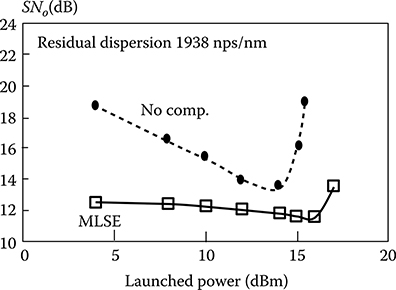
Figure 5.62 Performance of the MLSE EDC compared with that of a similar uncompensated receiver in the case of 10 Gbit/s speed. The total fiber link length was 214 km with a nominal dispersion value at 1550 nm of 17 ps/(nm km) and part of the dispersion is optically compensated at the receiver. The amount of transmitted power was varied to evaluate the performance of the MLSE EDC against SPM as a function of residual chromatic dispersion. The baseline SN0 is about 12 dB due to the use of the FEC at the receiver.
(After Downie, J.D. et al., IEEE Photon. Technol. Lett., 19(13), 1017, 2007.)
The EDC figure of merit is always the increment of the optical signal to noise ratio (Δ SNo) needed to overcome the effect of dispersion in a receiver equipped with a standard FEC.
Even if MLSE algorithms perform better even in their most reduced form, the circuitry implementing MLSE is in any case much more complex with respect to the circuitry implementing an FFE–DFE and it requires a much more complex design. This is going to influence prices of MLSE equalizers, at least up to the moment in which they will be diffused in large volumes.
Moreover, if an FFE–DFE introduces slight modifications to the signal statistical distribution, the MLSE changes it more radically.
As a matter of fact, MLSE is a sort of convolution decoding and the surviving errors at the MLSE output have characteristic configurations depending on the MLSE structure [86]. This affects the performances of a traditional FEC. Optimum performances are achieved by a joined design of the MLSE and the FEC so that the interaction between the two algorithms takes into account the correct noise statistics and optimizes the performances of both FEC and MLSE [87]. At present this design is greatly constrained by memory requirements both in terms of memory quantity and memory-processor communication speed. However, it is possible that further progress in electronics will make this technology more accessible.
5.8.4 Pre-Equalization and Pre-Distortion Equalizers
A simple technique to avoid the intrinsic limitation of post equalization due to the presence of the nonlinear photodiode response is the implementation of electronic pre-compensation, that is, signal distortion in the transmitter before propagation.
This technique can be implemented, for example, by using an I/Q modulator, or a dual-drive Mach–Zehnder modulator.
The simpler scheme of signal pre-distortion that is meant for compensation of chromatic dispersion impairments is shown in Figure 5.63.
The principle of operation of this circuit is simple: the modulator is driven by two signals that are built in such a way that the modulator output coincides with the signal to be transmitted filtered by a filter whose spectral response is the inverse of the fiber dispersion spectral characteristics.
In general, this way of compensating linear distortion is prone to several mathematical difficulties related to the fact that the inverse frequency function can be impossible to define when the distorting filter has a big attenuation, so as to almost cancel the signal at those frequencies. Fortunately this is not the case with fiber dispersion, whose characteristic function is a pure phase filter, whose module is equal to 1 at all frequencies.
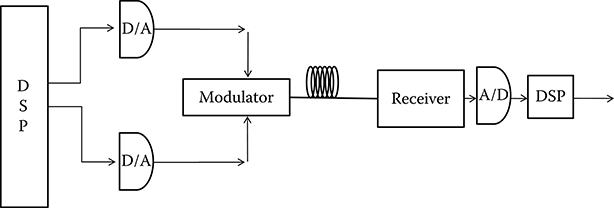
Figure 5.63 Block scheme of an electronic dispersion pre-compensator.
Thus, the driving currents for the modulator can be easily evaluated with simple calculations [88].
The pre-distortion filter implemented by the scheme of Figure 5.63 is quite effective in compensating large amounts of chromatic dispersion.
However, the pre-compensation technique allows the received pulse to be dispersion-free, but causes during propagation the broadening of the transmitted signals due to the combined effect of pre-distortion and dispersion.
This complex evolution, almost unavoidably, causes the apparition in some points along the link of complex structures with high maxima and deep depleted minima.
The high-power density maxima create a strong nonlinear effect, thus the pre-distorted signal is more prone to the nonlinear effect impairments with respect to a standard, non-compensated signal.
Nonlinear effects compensation can be operated in principle through the use of the so-called look-up table–based pre-distortion. This technique conceptually consists of the following steps:
A physical model of propagation through the link is implemented in a DSP, based on a nonlinear propagation equation like Equation 4.39; this model depends on a set of parameters that are specific to the link under operation.
At the beginning, in a set-up phase, the propagation model parameters are tuned by observing the link behavior when a set of known bit patterns is transmitted through the link. When a good estimate of the link parameters is reached they are used to fit the link behavior with the propagation algorithm.
Once the algorithm is tuned on the real link characteristics it is used to construct the inverse of the propagation operator through virtual pulse back-propagation through the link.
The inverse propagation operator is thus stored as a set of parameters in a look-up table that is used for fast pre-distortion during link operation.
The link enters operation and the transmitted pulses are pre-distorted using the data stored in the look-up table.
An adaptive algorithm adapts the look-up table parameters to the slow channel changes by repeating the link parameters identification periodically.
This method, based on back-propagation is also called electronic dynamically compensating transmission (EDCT).
A look-up table equalizer is quite effective, since its only limitation is the approximation implicit both in the propagation model and in the representation of the inverse propagation operator with a discrete set of numbers in a look-up table. Unfortunately, its direct application is at present difficult mainly due to the memory requirements that are difficult to satisfy with signal processors.
Thus, in order to exploit the idea of the look-up table algorithm, a mixed method is often proposed.
This scheme, represented in Figure 5.64, combines the look-up table technique with a further compensation through digital filtering [89]. The input bit sequence to be transmitted is used to address a look-up table, whose outputs values SI(j) and Sq(j) correspond to the real and imaginary parts of the waveform suitably distorted to compensate nonlinear effects. These values are input to a set of digital filters with transfer functions hRe(j) and hjm(j). The resulting in-phase and quadrature drive voltages d1 and d2 are then obtained by complex-summing the outputs of the filters as shown in the figure.
The equalizer resulting from the composition of digital filters and look-up table is potentially very efficient, requiring a much smaller memory table with respect to a direct application of the look-up table method.
Nevertheless, the great potentialities of this equalization method are not free from challenges that have to be solved for a practical implementation.
The first challenge is the complexity of the electronic circuitry with respect to a simple FFE–DFE post-processing. In the mixed solution represented in Figure 5.64, the set of linear filters consume alone about two times a traditional FFE–DFE filter. In addition, there is the look-up table. Finally there is the real-time adaptive algorithm that is needed to adapt equalization to the channel fluctuations.
The implementation of this algorithm is another challenge: if all the equalizer parameters have to be adapted to channel variations, the adaptive algorithm results in being quite complicated and a lot of design work is needed to implement it in a practical circuit.
Last, but not least, the adaptive algorithm needs a return channel from the receiver to the transmitter to drive transmitter-adaptive evolution with the received pulse shape. Thus, the receiver also must sample at a very high speed the incoming pulses to feed the transmission-adaptive procedure.
A complete study of the back-propagation algorithm in case of the adoption of a scalar propagation model and of the efficiency and complexity of this method is reported in [90].
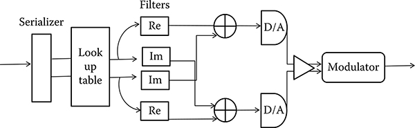
Figure 5.64 Scheme of an electronic pre-compensator that combines the look-up table technique with a further compensation through digital filtering.
(After Killey, R.I. et al., Electronic dispersion compensation by signal predistortion, Proceedings of Optical Fiber Conference, OSA, s.l., 2006.)
Starting from the propagation equation (Equation 4.39) it is demonstrated that the reverse propagation is obtained just from the forward propagation equation with negative parameters.
In this way, the signal attenuation is transformed into a gain and the operators working on the phase of the signal induce a rotation into the opposite direction.
Thus, to obtain the input signal corresponding to a certain output (i.e., the unperturbed signal) it is sufficient to “invert” the parameters of the propagation equation and to apply the split-step Fourier method, the same that is used to simulate fiber propagation in normal conditions [91].
From a processing complexity point of view, the signal processing block at the transmitter is one of the critical components.
In a practical system this block can be either implemented as an ASIC or by using a DSP or an FPGA. It is worth noting that in this case the ASIC solution could prevail even if it is more expensive and time-consuming due to its optimization, which could allow the consumed power to be reduced reentering within the system limits while achieving higher processing speed.
If the pulse distortion is mainly caused by linear propagation and nonlinear effects are negligible, the complexity of this device is mainly driven by the number of complex taps necessary for the FIR filter to compensate for the chromatic dispersion.
Several studies have been done to optimize the number of taps that can be adopted in this case [92] and it is demonstrated that the complexity scales linearly with the amount of accumulated dispersion to be compensated. It was shown that the complexity grows quadratically with an increasing bit rate [90].
In the presence of substantial nonlinear effects, nonlinear filtering has to be used. When a look-up table is used for filtering, the number of entries is determined by the number ζ of symbols that significantly interfere with each other. In particular, the number of look-up table entries grows exponentially according to Θζ, where Θ is the number of bits per symbol used in the signal sampling by the algorithm.
Regarding the channel memory, this is mainly due to dispersion; when dispersion is compensated optically and only intra-channel nonlinearity is compensated by EDCT, the number of entries remains relatively small.
However, for the joint compensation of chromatic dispersion and intra-channel nonlinearity the number of states can get rapidly impractical, especially beyond 10 Gbit/s. This does not only lead to increased storage requirements but it also increases the effort that needs to be spent on computation of pre-distorted waveforms.
In spite of all these challenges, the evolution of electronics technology for signal processing is rapidly eliminating the gap between the algorithm needs and the processing capabilities and similar methods are starting to be implemented in real products [93].
5.8.5 Forward Error Correction
The use of FEC is really instrumental in designing high-performance WDM systems, but has a much wider application field, comprising consumer electronics like PCs (in the transmission between the hard disc and the motherboard).
5.8.5.1 FEC Definition and Functionalities
An FEC is from a functional point of view an extension of the well-known error-detecting code that is able to correct the channel-induced errors if the error rate is within the correction ability of the code [94].
We will consider in this paragraph systematic block group codes without memory.
A code is a block code if the uncoded message is divided at the encoder in words of the same length and every word is processed by the encoder so as to obtain a longer word (called the code word).
Let us assume that the encoder receives a message constituted by a string of symbols extracted from the message alphabet M, a collection of M symbols, that is, ≡ {χj, j = 1,…, M}. We will assume that the code word is composed of the same symbols of the message word. Thus the encoder transforms message words of m symbols into code words of ɗ symbols all from the same alphabet the difference s = ɗ − m is called code redundancy.
Due to the encoding the line rate RLine results in being greater than the message rate Rmess, being Rline = (1 + (s/ɗ)Rmess).
A block code is systematic when the code word is obtained by adding to the message word a string of s symbols calculated by the encoder, but the message word is transmitted unchanged.
A block code is said to be without memory when every code word is created at the encoder independently from the previous words and is processed at the decoder also independently from the previous words. Every possible channel memory is considered contained in the length of the message word.
Finally a block code is called a group code when its coding and decoding algorithms are based on the fact that the alphabet M is structured as a group by defining suitable operations among its members. We will always consider codes built on alphabets that are at least rings (which have the structure of the integer numbers). In the most common cases in optical communications the alphabet structure is even richer, that is, it has the Galois field structure, which we will call G(M). This is the structure of the real numbers, but for the fact that the alphabet is constituted by a finite number of elements, differently from the real numbers.
Practically all the FECs used in optical communications have the properties considered in the aforementioned list, due to the fact that the encoding and decoding algorithms have to be performed in real time in pace with the arriving bit stream, whose speed is a minimum of 10 Gbit/s if not 40 or 100 [95–98]. This trend, however, is going to change with the need of more efficient codes for 100 Gbit/s transmission; at the end of this section we will look at one of the possible solutions for the next-generation codes: the turbo block codes.
A block code can correct errors since not all the words of ɗ symbols are possible code words, but only a subset of Mm words are acceptable. Thus, when an unacceptable word is detected, errors are revealed and, starting from the received word, an algorithm exists to estimate the transmitted word.
The number of nonzero symbols in the difference between two words of ɗ symbols in G(M) is called distance between the words and it is possible to verify that it has all the properties of a well-defined distance. The minimum distance between two code words is called Hamming distance of the code and it is quite clear that the upper bound of the number of errors that the code can correct is exactly the Hamming distance. As a matter of fact, changing a number of symbols equal to the Hamming distance is possible to change a code word into another code word, creating an error that is impossible to correct.
The Galois fields that are used in the block codes commonly used in optical transmission are the fields constituted by the integer numbers module for a given field-generating number ℘ which has to be a prime or the power of a prime; such fields are called G(℘). As an example, G(5) = {0, 1, 2, 3, 4}, where all the numbers have to be an intended module 5, so that, within G(5), 4 + 3 = 2 mod(5).
The symbols of the alphabet M are considered elements of G(M) so as to be able to perform operations with them. On the grounds of this definition, every word is represented with a polynomial in G(M), associating to the finite sequence of symbols {χj, j = 1, …, d} the polynomial P(y)=∑d−1j=0χj+1yj![]() .
.
With this definition, encoding and decoding algorithms can be structured as an operation with polynomials on G(M), the type of operation that a dedicated logic like that of an ASIC or of a DSP executes very fast.
Different codes can be defined depending on the encoding and decoding algorithms; each code is characterized by a correction capability (number of independent errors the code can correct in a received word), a detection capability (number of errors the code can detect, but not correct, in a received code word), and a degree of complexity of the encode and decode algorithms.
5.8.5.2 BCH and the Reed–Solomon Codes
The category of codes that are more effective in providing a good error correction capability with simple implementation algorithms are the Bose–Chaudhuri–Hocquenghem (BCH) codes (named after their inventors). Reed–Solomon (RS) codes, even if historically invented independently, are a category of BCH codes and are the most used in high-speed transmission.
The encoding algorithm of BCH codes is based on the multiplication of the mth degree polynomial representing the message word by a generating degree & polynomial ɡ(x) so as to derive the ɗth degree polynomial representing the code word.
The encoder can thus be implemented as a very simple linear feedback shift register (LFSR) as shown in Figure 5.65.
The characteristics of a particular BCH code depend on the choice of the generating polynomial.
To describe the way in which the generating polynomial is constructed, let us fix a generating prime number ℘, which is introduced to construct the code in G(℘ ). Naturally in many cases of interest ℘ = 2.

Figure 5.65 Bock scheme of a BCH encoder.
To search a code with a given Hamming distance, start to choose two positive integers ɗ and c such that ɗ and ℘ are reciprocally prime in G(℘m) (their unique common divisor is 1) and m is the multiplicative order of ℘ modulo ɗ.
To construct the generating polynomial it is needed to find the elements (ac+j, j = 1, …, &) where a is a primitive ɗth root of unit in G(℘m). In correspondence of each of the ac+j it is possible to find a minimal polynomial over G(℘), that is the minimum degree polynomial in the considered field with leading coefficient equal to 1 and having ac+j as radix; let us call it μj(χ).
The BCH code-generating polynomial is given by g(x) = lcm(μj(χ), j = 1, …), where lcm() indicates the lowest common multiple.
From the definitions, we can also say that a given word of ɗ symbols χj in Γ(℘m) is a code word if and only if the polynomial P(x)=∑d−1j=0χj+1xj![]() has all the elements ac+j as radix.
has all the elements ac+j as radix.
The construction we have described assures to the BCH code a minimum Hamming distance equal to δ and the ability to correct up to δ independent errors for each code word.
RS codes are particular BCH codes, where c = 0 and the generating polynomial is given by
g(x)=δ∏(j=1)(x−aj)ù(5.48)
![]()
(5.48)
As far as decoding is concerned, there are many algorithms to decode BCH codes; we will describe the most used here, due to its easy implementation at high speed.
At the decoder the received word composed by ɗ symbols is considered as a polynomial generated by the channel, adding to the sent polynomial t(χ) an error polynomial e(χ) so that correcting errors means determining e(χ) and subtracting it.
The algorithm steps are essentially three:
Compute the & syndromes ξj of the received word, which are defined as ξj = t(ac+j). It is evident that if all the syndromes are zero the word is a code word and it is considered correct. If not, there are errors to correct.
Starting from the syndromes find the error polynomial e(χ).
Reconstruct the correct code word as c(x)= t(χ)–e(χ).
The second step, that is the core of the algorithm, is not obvious, and it is not within the scope of this section to detail a procedure to determine the error polynomial starting from the syndromes.
There are two main algorithms to do that: the Peterson–Gorenstein–Zierler algorithm and the Berlekamp–Massey algorithm, both based on a set of linear operations on matrixes and vectors in the space (℘m).
Both the algorithms for their nature are well adapted to be implemented in a dedicated signal-processing circuit, and this is the reason for the wide adoption especially of the RS codes, for which the algorithm can be further simplified.
In general, the BCH decoder has the bock scheme represented in Figure 5.59.
5.8.5.3 Turbo Codes
The BCH codes, and the RS that are a particular class of BCH, guarantee a simple coding/decoding algorithm that is suitable for application at very high speed, but are far from the optimality since the capacity of a channel using BCH codes is far from the Shannon limit [94], even if very long code words are selected.

Figure 5.66 Principle scheme of a BCH decoder.

Figure 5.67 Composition of the code word of a systematic turbo block code.
This indicates that much better codes must exist, guaranteeing a higher number of corrected errors for a certain redundancy and code word length.
A class of better codes that is also suitable for application at high speed is constituted by the so-called turbo codes [99,100].
Turbo codes are a class of codes that construct the code word by concatenating two codes separated by an interleaver (see Figure 5.66).
The turbo code word, when the component codes are systematic, can be arranged in a matrix, whose rows are transmitted in a determined order, as shown in Figure 5.67, where it is clear that redundancy is added not only to check errors in the message, but also to check errors in the redundancy introduced by the composing codes.
As a result of the aforementioned definition, the encoder can be built from the encoders of the constituting codes so that the encoder of a systematic turbo code will appear as in Figure 5.68.
Starting from its very general definition, there are several classes of turbo codes: with and without memory (convolution or block codes), systematic or not (i.e., such that the redundancy is separated by the original message at the output or not).
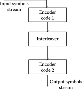
Figure 5.68 Encoder for a systematic turbo block code.
Since we target codes that can be applied in optical systems at a very high speed, we limit our attention to block turbo codes based on two equal BCH components, which results naturally as systematic codes.
The choice of the interleaver is a crucial part in the turbo code design. The task of the interleaver is to scramble the symbols in a predetermined way. The presence of the interleaver has two beneficial effects on the code.
The presence of code words with a high number of null symbols (in case of the BCH codes the zero of the Galois field) weakens the code, since in general they are separated by a smaller distance. From this it derives the general property that a good code has the highest possible average weight, where the code weight is defined as the average of the weight of the code words, that is, the average of nonzero symbols in the code words.
Now, in a turbo code, if the first encoder produces a low-weight word, it is improbable that the second also will do the same after scrambling. Generally it can be seen that scrambling increases the average weight of the code word, while decreasing at the same time its variability.
A second advantage of scrambling is constituted by the fact that decreasing the correlation between the two coded words that are transmitted increases the information that is sent to the decoder, thus allowing more effective decoders to be designed.
Ideally both these advantages are maximized by using a random scrambler, but it is difficult to realize at the high speeds typical of optical systems.
In Figure 5.69 the workings of a few possible interleaver designs are shown for the cases in which the sequences to be interleaved are binary [101].
Row–column interleaver: In this type of interleaver the data are written row-wise and read column-wise. This is a very simple design, adapted for use at very high speed, but it also provides little randomness.
Helical interleaver: In this type of interleaver, data are written row-wise and read diagonally.
Odd–even interleaver: In this encoder architecture, encoding happens before interleaving, and after encoding only the odd-positioned coded bits are stored. Then, the bits are scrambled and encoded again, but now only the even-positioned coded bits are stored.
The idea at the base of the decoder of turbo codes is that the signal arriving at the receiver is composed of two words encoded with the same code where the symbols are in a different order.
It is intuitive, even if it is not so easy to demonstrate, that the quantity of information the decoder has on the sent word is much greater than what it would have if only one code were used.

Figure 5.69 Scheme of the operation of a few possible interleaver algorithms.
In this situation, the generic decoder of a turbo code is a sort of soft decoder having at the input the row samples of the received data and constituted by two different decoders, one for each component code.
The decoders exchange information about the received word and at the end, if no errors happen, both produce the same output symbol stream.
Naturally, if the two decoders produce in a certain step two different outputs, they detect it by exchanging data, and interpret it as the presence of errors starting a joined procedure to determine the nature of the error and to correct it.
All this procedure is much more complicated than the decoding algorithm of BCH codes, but nevertheless can be carried out fast using dedicated logic, like a very fast DSP or FPGA or more probably an ASIC.
There is a strong research effort to study properties and implementation of turbo code decoders and the interested reader can start from the following bibliographies [102,103].
5.8.5.4 ITU-T OTN Standard and Advanced FEC
The use of a FEC implies that besides the signal to be transmitted, a redundancy is sent to be used by the decoder to correct decision errors or to perform optimum soft decision.
Since this redundancy has to be placed within the transmitted frame, it is natural to compare the requirement of the most performing codes that are suitable for optical transmission application with the ITU-T frame standard for optical transmission.
Currently, ITU-T has standardized the use of codes with 7% redundancy (exactly 16 bit redundancy and 255 bits overall length), as recommended in ITU-T G.975 and its successor ITU-T G.975.1. A 7% code is applied directly to blocks of binary information bits, producing an output sequence, whose length is expanded by a factor of 255/239, and the resulting bit stream is transmitted using a binary modulation format. That is, redundancy is accommodated by sending more symbols.
The research on transmission systems, however, is going toward a different direction.
As we will see in Chapter 9, in order to transmit speeds higher than 40 Gbit/s binary modulation is not suitable and multilevel coding is a very attractive solution. When multilevel coding is used, redundancy can be either transmitted by increasing the symbol rate or by increasing the number of symbols. For example, if a 16-level transmission is used, redundancy can be accommodated by passing to 32 levels. This means that one redundant bit is transmitted every three message bits.
As far as specific codes are concerned, the RS (255, 239) code was the first to see wide-spread application in fiber-optic communication systems, due to its high rate, good performance, and efficient hard-decision decoding algorithm.
As the speed of electronics increased, it became practical to consider more powerful error-correcting codes. The ITU-T G.975.1 standard describes several candidate codes providing better correction performances, all with a 16/255 structure in order to be accommodated into the Optical Transport Network (OTN) frame in place of the RS (255, 239).
In all the considered cases, hard-decision decoding is applied, and improved performance can be partially attributed to the significantly longer block lengths considered.
Due to the period in which this standard has been developed, no soft decision and no block turbo codes have been considered.
Even if the optical community has, so far, standardized FEC at 7% redundancy, this choice is not at all fundamental. The 7% value certainly reflects a reasonable choice of code rate, given the manner in which optical communication systems have been operated to date.
Due to the high SN of optical channels, the uncoded symbol error rate for binary signaling schemes is small. For the RS (255, 239) code, communication with bit error rates less than 10−12 requires an uncoded error rate (or “FEC threshold”) of less than 1.5 × 10⁻⁴.
Since optical systems have traditionally been operated to achieve such low pre-FEC error rates, a high-rate code was sufficient to provide sizeable coding gains, and 7% redundancy provided a reasonable balance between bit rate and error-correcting capability.
From an information theoretic perspective, however, mandating 7% redundancy unnecessarily restricts the pre-FEC symbol error rate to be small.
When multilevel transmission will come into play, that seems a must for transmission at 100 Gbit/s; this implies that the used multilevel constellation has to include a small number of points so as not to cause too big an SN penalty (see Chapter 9).
To increase the spectral efficiency of fiber-optic communication systems (e.g., via multilevel modulation), it is necessary to design the coded modulation scheme using information theoretic considerations. Maximizing spectral efficiency may, in fact, lead to operating points in which the “raw” error rate requires the use of codes with greater than 7% redundancy.
In view of the next-generation systems, this discussion will be opened inside the ITU-T and for sure, if effective proposals will emerge, standardization will include them into the standard.
The opportunity to do so will be standardization of multilevel optical systems, which are all to be developed since only binary systems are covered by today’s ITU-T recommendations.
Due to these considerations, in all our examples, we will not limit our self to consider 7% redundancy codes, even when binary systems are considered.
5.8.5.5 FEC Performances
A great effort of research has been devoted to determine the performances of various FECs in terms of SN gain. In the case of optical systems, the results obtained in the FEC-related literature have to be elaborated due to the particular form of the optical receiver.
As a matter of fact, we will see in Chapter 6 that the most important application of FEC is in long-haul and ultra-long-haul systems. In this case the error probability depends on the optical signal to noise ratio (SNo), which is in turn proportional to the optical received power. In general the FEC performances are provided in terms of gain on the SN immediately before decision, which in the optical case is the electrical signal to noise ratio (SNe).
In order to evaluate the performances in terms of optical gain, we have to link the SNo with the SNe using the receiver parameters.
Even if this relationship can be derived in a general way, this is not so significant. The most important cases are the two extreme cases in which there is no optical noise and the receiver noise plus shot noise dominates and the case in which the optical noise dominates.
As detailed in Chapter 6, these are the cases of unamplified systems and optically amplified systems.
In the first case, assuming as always in practice that the received optical signal can be modeled as a time sequence of coherent states, the overall noise after detection is equal to the variance of the shot noise plus the electronic noise (see Section 5.4).
Thus the electrical SN can be written as
SNe=R2pP2o2ħωBe+Fa(4kBℑ/RL)Be(5.49)
(5.49)
as obviously the SNe depends on the square of the optical power; thus a gain of X dB in SNe results in a gain of X/2 dB in terms of optical received power.
In the case of dominant optical noise, the SNo can be written in general as
SNo=PoPASE(5.50)
![]()
(5.50)
where PASE is the ASE power in the optical bandwidth.
On the other hand, the SNe has to be evaluated taking into account the quadratic detection law of the photodiode and neglecting shot noise and receiver noise.
In evaluating SNe we do not neglect the quadratic term in the noise, due to the fact that in the presence of FEC sometimes it is possible to work with a small SNe and the quadratic term in the noise can be relevant in situations in which errors are possible.
The quadratic term power, after electrical filtering, is evaluated assuming a flat optical noise spectral density in the band Bo; thus after square law detection the power spectral density of the term containing the square of the noise is a triangle with base extending from −2Bo to 2Bo. This triangular power spectral density is filtered by an almost ideal electrical filter of unilateral bandwidth Be.
The receiver model with the definition of the relevant wavelength and frequency bandwidths is represented for clarity in Figure 5.70. The conventions in terms of bandwidths and SN definition that are shown in the figure will be maintained for the remaining part of the book.
The ASE noise is considered a white Gaussian noise with power spectral density Σ0 so that the ASE power in the optical bandwidth, with the definitions of Figure 5.61, could be defined as PASE = 2Σ0Bo. Since, in order to have a parameter tailored for the application we will study in Chapter 6, we have defined Bo as unilateral bandwidth, it is convenient to define a unilateral ASE spectrum; let us call it S0 = 2Σ0 so that the ASE power can be written as PASE = S0Bo.
The fact that this definition is useful to write simply the equations immediately results from the case of a receiver using a single pre-amplifier.
In the case of a single amplifier, considering the expression of the ASE spectral density deduced in Chapter 4, we have, Bo being unilateral,
PASE=ħωc(G−1)BoNFyields→S0=ħωc(G−1)NF(5.51)
![]()
(5.51)
where
ωc is the carrier angular frequency
NF is the amplifier noise factor
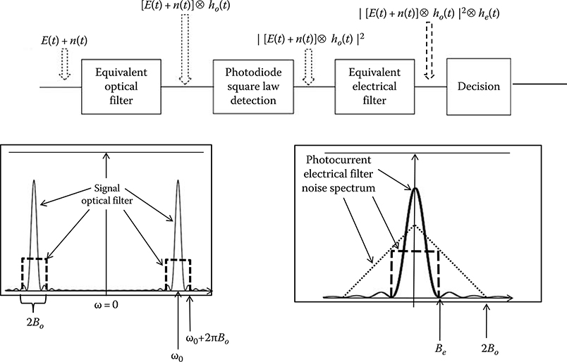
Figure 5.70 Definition of the formal receiver model used for the FEC performance evaluation and of the related bandwidths.
and the unilateral power spectral density S0 does not present any factor beyond the terms related to amplifier noise
On these grounds, the power of the electrical noise current corresponding to the optical noise is easily evaluated as
σ2=〈[n*(t)+E*r(t)n(t)+n(t)n*(t)]2〉=2PoS0Be+S202Be(4Bo−Be)(5.52)
![]()
(5.52)
where
Er(t) is the received field average
n(t) is the optical noise process whose average is supposed to be zero
Po, S0 are the signal power and the noise power spectral density, respectively
The electrical bandwidth is called Be and it is often approximated with the symbol rate Rs and the optical bandwidth (unilateral as defined in Figure 5.69) is called Bo.
Let us introduce the parameter Moe = Bo/Be > 0.5. It is the ratio between the electrical and the optical bandwidths, thus it is also the number of samples at the Nyquist sampling rate of the optical signal that fit into the Nyquist sampling interval. This parameter will be quite useful in the analysis of transmission systems.
As a function of Moe the electrical SN may be written as
SNe=P2o2PoSoBe+(S20/2)(4BoBe−B2e)=SN2oMoe2SNo+(2−1/2Moe)≈SNoMoe2(5.53)

(5.53)
where the approximation is valid in conditions of large SN, so that it can be written as SNo ≫ 1. In this case the SNs are equal if the electrical bandwidth is equal to half the unilateral optical bandwidth.
This relationship is plotted in Figure 5.71 for different values of Moe and it is the relation that has to be used to evaluate the code gain in systems with Gaussian noise.
It is to be noted that Figure 5.71 is plotted with SNo as an independent variable; decreasing Moe at constant SNo means that, for a constant value of the optical bandwidth, the electrical bandwidth shrinks so that less optical noise power is detected at the decision level. This explains why in the plot the SNe increases, decreasing the electrical bandwidth.

Figure 5.71 Relation between the optical signal to noise ratio (SNo) and the electrical signal to noise ratio (SNe) for different values of the ratio Moe between the optical bandwidth and the electrical unilateral bandwidth (Bo/Be).
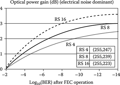
Figure 5.72 SNo gain of three different RS codes in an unamplified system.
In Figure 5.72 the gain of a few RS codes is plotted versus the target value of the BER (logarithm of the target BER after FEC operation) when no optical noise is present. The greater the code overheard, the greater is the code gain, even if in this case there is a modest gain due to the fact that SNe depends on the square of the optical power while the noise is added after square law detection.
The FEC gain curve is shown in Figure 5.73 for the case in which the optical noise is dominant. In this case the FEC allows higher gains to be achieved. It is to be underlined that the FEC gain decreases at the increase of Moe. This is due to the fact that in this case the plot is made maintaining constant the BER, and thus the SNe.
Inverting (5.53) we obtain
SNo=SNeMoe[1+√1+1SNe(2−12Moe)](5.54)
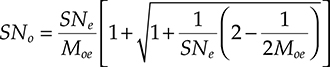
(5.54)
Thus it is evident that increasing Moe while SNe is constant means decreasing SNo, making clear the behavior of the curves of Figure 5.72.
From Figure 5.72 it is also derived that in the reference case Moe=2, when the standard code RS (233, 249) (indicated with RS8 in this Figure) is used to reach a BER of 10−12, a coding gain of 6 dB is attained.
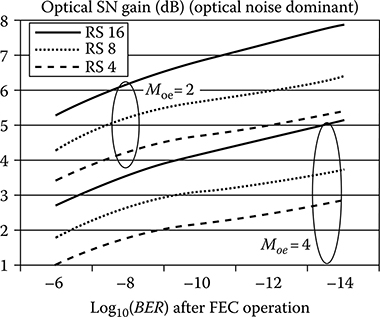
Figure 5.73 SNo gain of three different RS codes in a system with inline amplifiers so that the performances are dominated by the optical noise. RS (233, 249) is indicated with RS8.
Another useful manner to evaluate the effectiveness of an FEC that does not need to take into account the receiver parameters is to relate the error probability that would characterize the system without FEC with the error probability of the system with FEC. Generally these error probabilities are called pre-FEC and post-FEC BER.
Once the pre-FEC BER is determined the entire system is designed so as to obtain the wanted pre-FEC BER. After the addition of the FEC, the real error probability is determined by the pre-FEC BER and by the FEC performances.
The relation between the pre-FEC and the post-FEC BER is shown in Figure 5.73 for a few BCH codes.
As far as turbo codes are concerned, several codes have been constructed with encoder and decoder and analyzed.
An example is given in Figure 5.74, where the code gain in terms of SNe is shown for three block turbo codes built on RS codes [104]. In particular, the following component codes are selected:
Code A: built on RS (15, 12), redundancy 36%, Hamming distance 4
Code B: built on RS (31, 26), redundancy 30%, Hamming distance 6
Code C: built on RS (63, 58), redundancy 15%, Hamming distance 6
From the figure it is evident that the code gain is very high, also for the high redundancy that these codes exhibit, and in particular a code gain a little below 10 dB can be achieved at BER = 10−12.
The last observation to be made on the FEC performances is that we have assumed up to now a Gaussian distribution of the decision samples.
In reality we will see in Chapter 6 that this is not true: due to the square law detector, when the dominant noise is the ASE noise, the decision samples do not have a Gaussian distribution.

Figure 5.74 Relationship between pre-FEC BER and post-FEC BER for various BCH and RS codes.
It can be demonstrated that, taking into account the correct distribution of the electrical equivalent noise, the performances of the FEC gets better, less for BCH codes, while sometimes a more significant difference occurs in turbo codes [100].
This observation allows us to set the target for an advanced FEC to use in ultra-highspeed DWDM systems, to 11 dB of code gain.
5.8.6 Content Addressable Memories
As equalization and error correction is instrumental for high-capacity transmission, fast packet routing is fundamental to build the IP convergent network.
As detailed in Chapter 7, IP routers and carrier-class Ethernet switches have to compare the address of each incoming packet with the entries of a routing table, whose content indicates the output port where the packet has to be sent.
In the IP case, the operation is worsened by the fact that the so-called forwarding table does not contain whole addresses, but only prefixes, and routing is performed by searching the longest prefix matching the incoming IP address (see Chapter 3).
Since this operation has to be performed several million times a second, it is natural that in large packet switches it is carried out by specialized hardware whose core is generally a content-addressable memory (CAM) [105].
CAM is a derivation of the random access memory (RAM). In addition to the conventional READ and WRITE operations typical of RAMs, CAMs also support the SEARCH operations. A CAM stores a number of data words and compares a search key with all the stored entries in parallel. If a match is found, the corresponding memory location is retrieved. In the presence of multiple matches, either several addresses are returned or a priority encoder determines the highest priority match on the grounds of a matching priority policy (Figure 5.75).
CAM-based table look-up is very fast due to the parallel nature of the SEARCH operation. A schematic illustration of the CAM working is shown in Figure 5.76.
CAMs can be divided into two categories: binary CAMs and ternary content-addressable memories (TCAMs). A binary CAM can store and search binary words (made of “0”s and “1”s). Thus, binary CAMs are suitable for applications that require only exact-match searches. A more powerful and feature-rich TCAM can store and search ternary states (“1,” “0,” and “X”). The state “X”, also called “mask” or “don’t care,” can be used as a wild-card entry to perform partial matching.

Figure 5.75 Coding gain for a few block turbo codes based on RS code components. The code characteristics are listed in the text.

Figure 5.76 CAM functional scheme.
A typical CAM cell utilizing 10 transistors all in CMOS configuration (a 10 T cell) is shown in Figure 5.77. The bottom part of the figure (transistors from T1 to T6) replicates exactly the structure of an SRAM cell and is used to perform READ and WRITE operations.
The transistors from T7 to T10 implement the XNOR logic that is needed during the SEARCH to compare the table entry with the search key.
As in a SRAM, The WRITE operation is performed by placing the data on the bit lines (Bs) and enabling the word line. This turns on the access CMOS (T1–T2), and the internal nodes of the cross-coupled inverters are written by the data. The READ operation is performed by pre-charging the Bs to the power supply voltage VD and enabling the word line.

Figure 5.77 Circuit representation of a CAM cell.
The conventional SEARCH operation is performed in steps:
Search lines (S and S′) are reset to ground.
M is pre-charged to VD.
The search key bit and its complementary value are placed on S and S′.
If the search key bit is identical to the stored value (S = B, S′ = B′), both M-to-ground pull-down paths remain “OFF,” and the M remains at VD indicating a “match.”
Otherwise, if the search key bit is different from the stored value, one of the pull-down paths conducts and discharges M-to-ground indicating a “mismatch.”
A TCAM cell is conceptually similar to the CAM cell, but it needs two SRAM cells to be able to store ternary data.
Several variations have been proposed for the base cell architecture that is shown in Figure 5.77, all with the intent to lower the voltage and power consumption and/or to increase the cell speed [106–108], and at present every practical CAM and TCAM implementation, even if it relies on the same base principle, has its own design particularity.
A CAM or a TCAM is realized by a matrix of cells, not so differently from an SRAM. The matrix lines represent the stored words, sharing the M voltage terminal that is connected with the so-called M sense amplifier, which detects the presence or the absence of a match with the search word that is stored in a suitable registry. This architecture is shown in Figure 5.78.
Besides the pure dedicated hardware implementation that we have briefly described, the progress in terms of density of CMOS circuits have recently allowed the CAM and TCAM implementation via FPGAs using suitably optimized libraries [109].
In terms of performances, the main CAM parameters are
Search speed (measured in terms of msps, or mega searches per second)
The power consumption during the search operation

Figure 5.78 A complete CAM composed of an array of CAM cells.
The dimension of the searchable area (traditionally the length of the CAM word is called width and the number of the word depth so that generally the capacity is called CAM area)
Flexibility
As far as the speed is concerned, it is the search speed that is to be reported since in the main CAM and TCAM application, that is, router-forwarding engines and MAC-routing switches, the memory performs almost only search operations, being read and written only when the routing table is updated.
Flexibility indicates the possibility to use the CAM to perform different types of operations. Commercial CAMs frequently can be configured either as real CAM or as TCAM depending on the activation of a mask flag. Another configurable feature is the priority policy, whose parameters can be set via a CAM control. Sometimes the priority mechanism can also be disabled so that all the found matches are reported at the output.
A CAM/TCAM realized with dedicated hardware and CMOS 65 nm technology can reach 100 Mbit capacity with a width comprising between 40 and 640 bits. With a suitable clock speed (around 360 MHz) the search speed can arrive at 360 Msearch/s, all in a processor-like package 30 × 30 mm.
Perhaps the most critical performance of large CAM/TCAM is the power consumption and much industrial effort is directed to reduce it. A TCAM having the performances summarized in the earlier paragraph can consume about 15 W. Taking into account that in order to design a core router packet-forwarding engine eight TCAMs could be needed, a power consumption up to 120 W can result.
A possible way to reduce power consumption is to cascade different pipelines in the CAM/TCAM architecture, as shown in [107]. In this case, maintaining a low latency, which means limiting the number of cascaded pipelines, an energy consumption as low as 7 W seems attainable.
Another possible approach is to use FPGAs to program the CAM/TCAM functionality. In principle, FPGAs are general-purpose chips, being thus less optimized with respect to a specific dedicated hardware.
In practice, the huge volumes and the large application domain of FPGAs have pushed a rapid improvement of performances via so good a design optimization that sometimes they are competitive with dedicated chips.
From a density and power consumption point of view, the last three generations of FPGAs have seen the density scale from 10 k gates to 300 k gates and the power consumption from 30 to 12 W (see Section 5.7.3) [110]. Therefore it is possible in some conditions to spare a few watts using FPGAs, with the advantage that they allow working with volumes smaller than that necessary to fully justify the ASIC development expenses.
5.9 Interface Modules and Transceivers
When optical transmission was born, optical systems were produced by vertically integrated companies, manufacturing in-house all the key components that should be integrated into the WDM system.
With the consolidation of the technology and the decrease of the margins due to the so-called bubble crisis, the companies in the optical communication market concentrated their effort on the core business, separating the activities in other areas.
Contemporary to this market evolution, technology was going on producing more and more classes of different devices for different applications.
Thus system vendors faced a double problem: first, it was difficult to develop in-house the electronic control of components that was manufactured outside; as a matter of fact, sometimes this is very hard without a direct knowledge of the mechanisms that are at the base of the component design (this is true, for example, for multi-section tunable lasers, several types of switches, and so on).
Moreover, in the absence of any standardization on the technology, every component has its own control and its own parameters; thus functionally equivalent components from different vendors cannot be exchanged, but each of them has to be driven by specific electronics.
This fact makes it impossible for system vendors to leverage on multiple suppliers to have better prices and manage the risk that one of them faces the impossibility to go on with the furniture.
In order to solve these two problems, system vendors started to ask components vendors for the so-called optical modules. These are subsystems that, in the simpler hypothesis, will contain a component with its own electronic control so that this subsystem can be directly mounted on the system card and be driven by the system controller through a digital interface with an appropriate language.
Even if single-component modules are quite popular as far as switches and similar components are concerned, in the case of the transmitting and receiving interfaces a further evolution has pushed the system and component vendors to define Multiple-Source Agreements (MSA) for more complex modules comprising both transmitter and receiver.
These optical interface modules can be divided into three classes:
MSA TX/RX modules
Fixed transceivers
Pluggable transceivers
The so-called MSA modules are generally DWDM-quality interfaces (even if gray and short-haul MSA also exist) that are designed to be directly integrated into the system card. They exit with two fiber pigtails and two connectors so that they can be connected with the transmission fibers.
In addition, fixed transceivers are modules that are mounted on the system card, but they are generally low-quality interfaces, designed more to occupy a small space and dissipate less power. Since a couple of years they have been completely substituted by pluggable transceivers.
Pluggable transceivers are interfaces, both WDM and gray, that are mounted on a package inserted into the hosting card from the front through a suitable housing while the system is running.
The transceiver is recognized and switched on by the system controller, all without interfering with the system working.
In this way, when a failure occurs, there is no need of changing the whole card, but it is possible to change only the transceiver.
Due to their small form factor, pluggable transceivers cannot host high-performance interfaces, which are still reserved for MSA modules, but miniaturization of lasers and electronics is going on and perhaps the day is not far when pluggable transceivers will substitute MSA modules as well.
5.9.1 MSA Transmitting–Receiving Modules
The MSA 300 PIN transponder is the standard interface for high-performance DWDM systems, especially if tunable lasers are required. It is standardized in two different dimensions: MMS (medium size) and SFF (small size).
The mechanical dimensions of the two standards with the positing on the package of the main features are depicted in Figures 5.79 and 5.80.
The name comes from the 300 PIN connector that is located on the lower part of the package and assures the contact of the transponder with the host card.
The functional scheme of a 300 PIN MSA transponder is sketched in Figure 5.81. From the figure it is evident that the scope of the transponder is to supply also the drivers to the system vendor, mainly for the laser and the modulator.
No signal processing is in general present inside the transponder: no FEC, no electronic compensator; the design of a few among these elements is perceived as a differentiator by the DWDM vendors so that it is not wanted inside a multivendor standard module.
However, it is possible that this will change at the moment in which the MSA 300 PIN at 10 Gbit/s will be in competition with the smaller XFP. At that moment it is possible that substantial signal processing will migrate inside the MSA 300 to differentiate it from the XFP.
The functional scheme evidences also the digital standard interface that MSA 300 PIN modules use to communicate with the motherboard: the I2C interface [52]. This is a simple standard, comprising a layered description of the transmission system that allows the motherboard both to configure the module and to read alarms coming from it.
As far as the MSA 300 PIN at 40 Gbit/s is concerned, no alternative format is present, since transceivers as they are standardized at present are not able to host 40 Gbit/s components, essentially for a power consumption and for a mechanical dimension reason.

Figure 5.79 External dimensions of an MMF MSA 300 PIN transponder.
Figure 5.80 External dimensions of an SMF MSA 300 PIN transponder.

Figure 5.81 Functional scheme of an MSA 300 PIN transponder.
TABLE 5.10 Parameters of Practical MSA 300 PIN Transponders
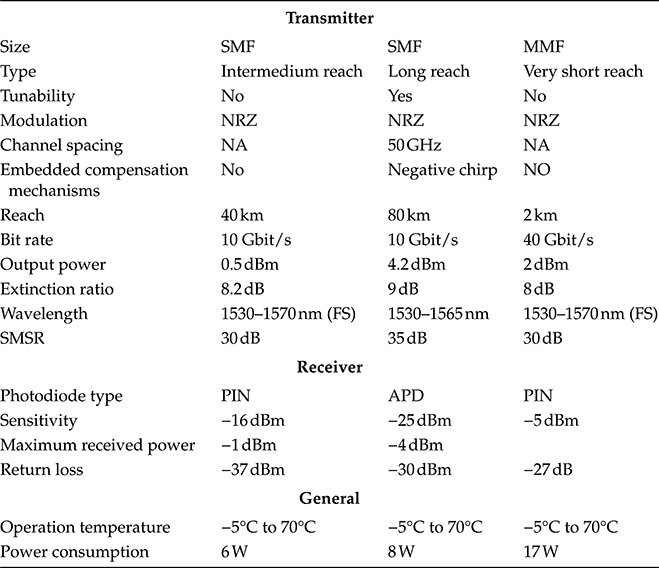
In Table 5.10 an overview of practical performances of MSA 300 PIN modules is reported.
5.9.2 Transceivers for Carrier-Class Transmission
Pluggable transceivers were introduced initially in datacom equipment as an advanced version of fixed transceivers. However, the advantages of pluggability and the small form factor were so appealing that telecom transceivers were introduced very soon.
There are a plethora of standard transceiver formats, but at present only two are really used in the telecommunication environment, the others being either confined to datacom application or completely substituted by more advanced formats: small form-factor pluggable (SFPs) and XFPs. Thus we will talk in detail only about these two standards.
5.9.2.1 SFP Transceivers for Telecommunications
The SFP is the more compact optical transceiver used in optical communications. It interfaces a network equipment mother board to a fiber-optic or unshielded twisted pair networking cable.
This is probably the most diffused transceiver format available with a variety of different transmitter and receiver types, allowing users to select the appropriate transceiver for each link to provide the required optical reach over the available optical fiber (e.g., multimode fiber or single-mode fiber).

Figure 5.82 Pictorial representation and dimensions of a pluggable SFP transceiver.
A drawing of an SFP transceiver is presented in Figure 5.82, where the particular connector for the input and output fibers that, with different dimensions, is present in all the transceivers is evidenced. The way in which the SFP transceivers are hosted on the motherboard using a suitable cage allowing a hot plug is shown in Figure 5.83, where both the empty cages on the front of a system card and the cages with plugged SFPs are shown.
Optical SFP modules are commonly available in four different categories: 850 nm (SX), 1310 nm (LX), 1550 nm (ZX), and WDM, both DWDM and CWDM. SFP transceivers are also available with a “copper” cable interface, allowing a host device designed primarily for optical fiber communications to also communicate over unshielded twisted pair networking cable.
Commercially available transceivers have a capability up to 2.5 Gbit/s for transmission applications; moreover, a version of the standard with a bit rate of 10 Gbit/s exists, but it can be used only to connect nearby equipment, and is very useful to spare space and power consumption as interface in the client cards of line equipments.
Modern optical SFP transceivers support digital optical monitoring functions according to the industry standard SFF-8472 MSA. This feature gives the end user the ability to monitor real-time parameters of the SFP, such as optical output power, optical input power, temperature, laser bias current, and transceiver supply voltage.
SFP transceivers are designed to support SONET, Gigabit Ethernet, Fiber Channel, and other communications standards.
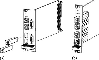
Figure 5.83 Hosting of SFP transceivers into a system card.
TABLE 5.11 Characteristics of Practical SFP Pluggable Transceivers for Different Applications

The standard is expanding to SFP+, which will be able to support data rates up to 10.0 Gbit/s (that will include the data rates for 8 Gbit Fiber Channel, and 10 GbE). Possible performances of different realistic SFP transceivers are reported in Table 5.11.
5.9.2.2 XFP Transceivers for Telecommunications
The MSA for the XFP transceiver was born after the start of the success of the SFP format to provide a transceiver with a form factor suitable to host 10 Gbit/s transmission components, but sufficiently compact to reproduce the advantages of the SFP.
In a short time it was evident that the XFP industrial standard was really tailored according to the system needs and at present this is the only type of transceiver used in telecom equipments whose evolution is targeted to high-performance interfaces at 10 Gbit/s.
At the beginning the target was a simple short-reach or medium-reach interface, but the evolution of the lasers and the Mach–Zehnder modulators integrated on InP platform is driving the development of a new generation of high-performance XFPs with tunable long-reach interfaces.
Thus, at present, there are a large number of different XFP transceivers designed for telecommunications: from the transceivers with gray short-reach interfaces for application in the client ports of optical equipments to short-, intermediate-, and long-reach DWDM interfaces, both with fixed and tunable lasers, to CWDM 10 Gbit/s transceivers.
The drawing of an XFP transceiver is presented in Figure 5.84 with the indication of the transceiver’s main dimensions. XFP transceivers are slightly greater than SFPs, but they are by far the smaller 10 Gbit/s interfaces suitable for DWDM transmission, and even if the transmission performances attainable with MSA 300 PIN are better, several optical systems, even when requiring long-haul transmission, adopt XFPs. As a matter of fact, the advantages in terms of space, power consumption, and failure management often over-compensate a certain transmission penalty.
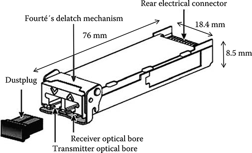
Figure 5.84 Pictorial representation and dimensions of a pluggable XFP transceiver.
The way an XFP is hosted on the motherboard is shown in Figure 5.85. As in the case of the SFP there is a suitable cage that has to be mounted on the motherboard in order to allow the XFP hot plug. Since high-performance XFPs have a high ratio between power consumption and area of contact with the cooling air flux, a heat sink is generally needed to increase the heat exchange area. This is mounted directly on the cage to minimize the thermal resistance (see Section 6.5).
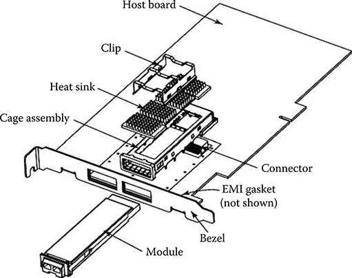
Figure 5.85 Hosting of XFP transceivers into a system card.

Figure 5.86 Functional scheme of a DWDM 10 Gbit/s XFP transceiver.
The functional diagram of a high-performance XFP is shown in Figure 5.86. From the figure it results that the module is controlled via an I2C interface, the same that is used also to control MSA 300 PIN modules. This clearly declares the fact that an XFP is not conceived as a low-performance module; on the contrary, it is equipped with a sufficiently powerful control interface to allow even the most complex features to be configured and managed.
TABLE 5.12 Characteristics of Practical DWDM XFP Transceivers Optimized for Different Uses

The input–output of the 10 Gbit/s channel is performed through the XFI parallel standard. This choice has been made to comply with the maximum possible number of system card design.
In Table 5.12 the main characteristics of three different DWDM XFPs are summarized.
REFERENCES
1.. Numai, T., Fundamentals of Semiconductor Lasers, Springer, New York, s.l., 2010, ISBN-13: 978-1441923516.
2.. Tsidilkovskii, I. M., Band Structure of Semiconductors, Pergamon Press, Oxford, NY, s.l., 1982, ISBN-13: 978-0080216577.
3.. Loudon, R., The Quantum Theory of Light, 3rd Edn., Oxford Science Publications, New York, s.l., 2000, ISBN 0198501765.
4.. Vahala, K., Yariv, A., Semiclassical theory of noise in semiconductor lasers: Part II, Journal of Quantum Electronics, 19(6), 1102–1109 (1983).
5.. Vey, J. L., Gallion, P., Semiclassical model of semiconductor laser noise and amplitude noise squeezing—Part I: Description and application to Fabry–Perot laser, IEEE Journal of Quantum Electronics, 33(11), 2097–2104 (1997).
6.. Hui, R., Mecozzi, A., D’Ottavi, A., Spano, P., Novel measurement technique of alpha factor in DFB semiconductor lasers by injection locking, Electronics Letters, 26(14), 997–998 (1990).
7.. Travagnin, M., Intensity and phase noise spectra in semiconductor lasers: A parallelism between the noise enhancing effect of pump blocking and nonlinear dispersion, Journal of Optics B: Quantum Semiclassical Optics, 2, L25–L29 (2000).
8.. Piazzolla, S., Spano, P., Tamburrini, M., Characterization of phase noise in semiconductor lasers, Applied Physics Letters, 41(8), 695–696 (1982).
9.. Mecozzi, A., Piazzolla, S., Sapia, A., Spano, P., Non-Gaussian statistics of frequency fluctuations in line-narrowed semiconductor lasers, IEEE Journal of Quantum Electronics, 24(10), 1985–1988 (1988).
10.. Aragon Photonics Application Note. Characterization of the main parameters of DFB using the BOSE. 2002, www.aragonphotonics.com (accessed: May 25, 2010).
11.. JDSU Application Note. Relative Intensity Noise, Phase Noise and Linewidth, JDSU Corporate, s.l., 2006, www.jdsu.com (accessed: May 25, 2010).
12.. Lewis, G. M., Smowton, P. M., Blood, P., Chow, W. W., Effect of tensile strain/well-width combination on the measured gain-radiative current characteristics of 635 nm laser diodes, Applied Physics Letters, 82(10), 1524–1527 (2003), doi: 10.1063/1.1559658
13.. Wentworth, R. H., Bodeep, G. E., Darcie, T. E., Laser mode partition noise in lightwave systems using dispersive optical fiber, Journal of Lightwave Technology, 10(1), 84–89 (1992).
14.. Iga, K., Surface-emitting laser—Its birth and generation of new optoelectronics field, IEEE Journal of Selected Areas in Quantum Electronics, 6(6), 1201–1215 (2000).
15.. Wistey, M. A., Bank, S. R., Bae, H. P., Yuen, H. B., Pickett, E. R., Goddard, L. L., Harris, J. S., GaInNAsSb = GaAs vertical cavity surface emitting lasers at 1534 nm, Electronics Letters, 42(5), 282–283 (2006).
16.. RayCan, 1550 nm Vertical-cavity surface-emitting laser. 090115 Rev 4.0.
17.. Jurcevic, P., Performance enhancement in CWDM systems, Diploma Thesys—Technischen Universitat Wien, s.n., Wien, Austria, May 2008.
18.. Björlin, E. S., Geske, J., Mehta, M., Piprek, J., Temperature dependence of the relaxation resonance frequency of long-wavelength vertical-cavity lasers, IEEE Photonics Technology Letters, 17(5), 944–946 (2005).
19.. Hofmann, W., Böhm, G., Ortsiefer, M., Wong, E., Amann, M.-C., Uncooled high speed (>11 GHz) 1.55 μm VCSELs for CWDM access networks, Proceedings of European Conference on Optical Communications—ECOC 2006, Cannes, France, September 24–28, s.n., 2006.
Kuznetsov, M., Theory of wavelength tuning in two-segment distributed, IEEE Journal of Quantum Electronics, 24(9), 1837–1844 (1988).
21.. Kobayashi, K., Mito, I., Single frequency and tunable laser diodes, IEEE Journal of Lightwave Technology, 6(11), 1623–1633 (1988).
22.. Yariv, A., Optical Electronics, 4th Edn., Saunders College, philadelphia, PA, s.l., 1991.
23.. Coldren, L. A., Monolithic tunable didoe lasers, IEEE Journal of Selected Areas in Quantum Electronics, 6(6), 988–999 (2000).
24.. Mason, B., Fish, G. A., Barton, J., Kaman, V., Coldren, L. A., Denbaars, S., Characteristics of sampling grating DBR lasers, Optical Fiber Conference 2000, Baltimore, MD, IEEE, s.l., March 2000.
25.. Born, M., Wolf, E. Principles of Optics: Electromagnetic Theory of Propagation, Interference and Diffraction of Light, 7th Edn, Cambridge University Press, Cambridge, U.K., s.l., 1999, ISBN-13: 978-0521642224.
26.. Ishii, H., Tanobe, H., Kano, F., Tohmori, Y., Kondo, Y., Yoshikuni, Y., Quasidiscontinuous wavelength tuning in a super-structure-grating, IEEE Journal of Quantum Electronics, 32(3), 433–441 (1966).
27.. Piotrowski, J., Rogalski, A., High-Operating-Temperature Infrared Photodetectors, SPIE Publications, Bellingham, WA, s.l., 2007, ISBN-13: 978-0819465351.
28.. Basu, P. K., Das, N. R., Mukhopadhyay, B., Sen, G., Das, M. K., Ge/Si photodetectors and group IV alloy based photodetector materials, Proceedings of 9th International Conference on Numerical Simulation of Optoelectronic Devices, NUSOD 2009, South Korea, IEEE, 2009, pp. 79–80, September 14–18, 2009.
29.. Mathews, J., Radek R., Xie, J., Yu, S.-Q., Menendez, J., Kouvetakis, J., Extended performance GeSn/Si(100) p-i-n photodetectors for full spectral range telecommunication applications, Applied Physics Letters, 95(13), 133506–133506–3 (2009).
30.. Campbell, J. C., Recent advances in telecommunications avalanche photodiodes, IEEE Journal of Lightwave Technology, 25, 109–121 (2007).
31.. Agrawal, G. P., Lightwave Technology: Components and Devices, Wiley, Hoboken, NJ, s.l., 2004, ISBN 047121 5732.
32.. Schneider, K., Zimmermann, H. K., Highly Sensitive Optical Receivers, Springer, Berlin, Germany, s.l., 2006, ISBN-13: 978-3540296133.
33.. Hunsperger, R. G., Integrated Optics: Theory and Technology, 6th Edn., Springer, New York, s.l., 2009, ISBN-13: 978-0387897745.
34.. Li, G. L., Yu, P. K. L., Optical intensity modulators for digital and analog applications, IEEE Journal of Lightwave Technology, 21(9), 2010–2030 (2003).
35.. Jackson, M. K., Smith, V. M., Hallam, W. J., Maycock, J. C., Optically linearized modulators: Chirp control for low-distortion analog transmission, IEEE Journal of Lightwave Technology, 15(8), 1538–1545 (1997).
36.. Muraro, A., Passaro, A., Abe, N. M., Preto, A. J., Stephany, S., Design of electrooptic modulators using a multiobjective optimization approach, IEEE Journal of Lightwave Technology, 26(16), 2969–2976 (2008).
37.. André, P. S., Pinto, J. L., Optimising the operation characteristics of a LiNbO3 based Mach Zehnder modulator, Journal of Optical Communications, 22, 767–773 (2001).
38.. Yasaka, H., Tsuzuki, K., Kikuchi, N., Ishikawa, N., Yasui, T., Shibata, Y., Advances in InP Mach-Zehnder modulators for large capacity photonic network systems, Proceedings of 20th International Conference on Indium Phosphide and Related Materials, IPRM 2008, Versailles, France, s.n., pp. 1–5, May 25–29, 2008.
39.. Prasad, P. N., Nanophotonics, Wiley, Hoboken, NJ, s.l., 2004, ISBN 0741649880.
40.. Yamanaka, T., Yokoyama, K., Design and analysis of low-chirp electroabsorption modulators using bandstructure engineering, 2nd Edn., Proceedings of Second International Workshop on Physics and Modeling of Devices Based on Low-Dimensional Structures, Aizu, Japan, 1998.
41.. Zhang, S. Z., Chiu, Y.-J., Abrham, P., Bowers, E., 25 GHz polarization insensitive electroabsorption modulators with traveling wave electrodes, IEEE Photonics Technology Letters, 11(2), 191–193 (1999).
Kahn, X., Zhu, J. M., Free-space optical communication through atmospheric turbulence channels, IEEE Transactions on Communications, 50(8), 1293–1300 (2002).
43.. El-Bawab, T. S., Optical Switching, Springer Verlag, New York, s.l., 2006, ISBN 0387261419.
44.. Liu, A.-Q., Photonic MEMS Devices: Design, Fabrication and Control, CRC Press, Boca Raton, FL, s.l., 2009, ISBN 139781420045600.
45.. Korvink, J. G., Paul, O., MEMS: A Practical Guide to Design, Analysis, and Applications, Springer Verlag & William Andrew, Heidelberg, Germany, s.l., 2006, ISBN 0815514972.
46.. Chigrinov, V. G., Pasechnik, S. V., Shmeliova, D. V., Liquid Crystals: Viscous and Elastic Properties in Theory and Applications, Wiley, Weinheim, Germany, s.l., 2009, ISBN 9783527407200.
47.. Parthasarathy, S. E., Thompson, S., Moors law, the future of Si microelectronics, Materials Today, 9(8), 20–25 (2006).
48.. ITRS, International Technology Roadmap for Semiconductors Industry, 2009 Edn., 2009, www.itrs.com (consulted: July 5, 2010).
49.. Roy, K., Yeo, K.-S., Low Voltage, Low Power VLSI Subsystems, McGraw Hill, New York, s.l., 2004, ISBN 007143786.
50.. Soudris, D., Pirsch, P., Barke, E., Integrated Circuit Design: Power and Timing Modeling, Optimization, and Simulation (10th Int. Workshop), Springer, Berlin, Germany, s.l., 2000, ISBN 3540410686.
51.. Lindsay, R., Pawlak, B., Kittl, J., Henson, K., Torregiani, C., Giangrandi, S., Surdeanu, R., Vandervorst, W., Mayur, A., Ross, J., McCoy, S., Gelpey, J., Elliott, K., Pages, X., Satta, A., Lauwers, A., Stolk, P., Maex, K., A Comparison of Spike, Flash, SPER and Laser Annealing for 45 nm CMOS. The Material Gateway, The Material Research Society, s.l., 2000, http://www.mrs.org/s_mrs/sec_subscribe.asp?CID = 2593&DID = 109911&action=detail (accessed: July 5, 2010).
52.. Storey, N., Electronics: A Systems Approach, 4th Edn., Pearson, Canada, s.l., 2009, ISBN 9780273719182.
53.. Veendrick, H. J. M., Nanometer CMOS ICs: From Basics to ASICs, Springer, Heidelberg, Germany, s.l., 2008, ISBN 9781402083327.
54.. Golshan, K., Physical Design Essentials: An ASIC Design Implementation Perspective, Springer, New York, s.l., 2010, ISBN-13: 978-1441942197.
55.. Beggs, B., Sitch, J., Future perspectives of CMOS technology for coherent receivers, European Conference on Optical Communications—ECOC 2009, Vienna, Austria, Vol. Workshop ‘DSP & FEC: towards the Shannon limit’, September 20–24, 2009.
56.. Papagiannakis, I., Klonidis, D., Curri, V., Poggiolini, P., Bosco, G., Killey, R. I., Omella, M., Prat, J., Fonseca, D., Teixeira, A., Cartaxo, A., Freund, R., Grivas, E., Bogris, A., Birbas, A. N., Tomkos, I., Electronic distortion compensation in the mitigation of optical transmission impairments: The view of joint project on mitigation of optical transmission impairments by electronic means ePhoton/ONe1 project, Optoelectronics, 3(2), 73–85, 2009.
57.. Walker, J., Sheikh, F., Mathew, S. K., Krishnamurthy, R., A Skein-512 Hardware Implementation, Intel Public Report, s.l., 2010, http://csrc.nist.gov/groups/ST/hash/sha-3/Round2/Aug2010/documents/papers/WALKER_skein-intel-hwd.pdf (accessed: October 18, 2010).
58.. Altera, Leveraging the 40-nm Process Node to Deliver the World’s Most, 2009. White Paper, www.altera.com (accessed October 18, 2010).
59.. Woods, R., McAllister, J., Turner, R., Yi, Y., Lightbody, G., FPGA-Based Implementation of Signal Processing Systems, Wiley, Chichester, U.K., s.l., 2008, ISBN-13: 978-0470030097.
60.. Brown, S., Rose, J., Architecture of FPGAs and CPLDs: A Tutorial, Department of Electrical and Computer Engineering, University of Toronto, Toronto, Ontario, Canada, 2000, http://www.eecg.toronto.edu/~jayar/pubs/brown/survey.pdf (accessed: October 18, 2010).
61.. Xlinx, Vertex Family FPGA Technical Documentation, 2010 version, www.xilinx.com (accessed: October 18, 2010).
62.. Actel, Technical Reference for Actel Antifuse FPGAs, 2010, www.Actel.com (accessed: October 18, 2010).
63.. Kestur, S., Davis, J. D., Williams, O., BLAS comparison on FPGA, CPU and GPU [a cura di], IEEE Computer Society, Annual Symposium on VLSI (ISVLSI), 2010, Lixouri Kefalonia, Greece, IEEE, s.l., pp. 288–293, 2010.
Chitode, J. S., Digital Signal Processing, Pune Technical Publications, Pune, India, s.l., 2008, ISBN 9788184311327.
65.. Ceva, The Architecture of Ceva DSPs—Product Note, 2010, www.ceva-dsp.com (accessed: October 18, 2010).
66.. Pederson, D. O., Mayaram, K., Analog Integrated Circuits for Communication: Principles, Simulation and Design, Springer, New York, s.l., 2010, ISBN-13: 978-1441943248.
67.. Tomkos, I., Spyropoulou, M., Ennser, K., Köhn, M., Mikac, B., Towards Digital Optical Networks: COST Action 291 Final Report, Springer, Berlin, Germany, s.l., 2009, ISBN 13 9783642015236.
68.. Säckinger, E., Broadband Circuits for Optical Fiber Communication, Wiley, Hoboken, NJ, s.l., 2005, ISBN: 978-0-471-71233-6.
69.. Chen, W.-K. (ed.), Fundamentals of Circuits and Filters, CRC Press, Boca Raton, FL, s.l., 2009, ISBN-13: 978-1420058871.
70.. Weber, C., Bunge, C.-A., Petermann, K., Fiber nonlinearities in systems using electronic pre-distortion of dispersion at 10 and 40 Gbit/s, IEEE Journal of Lightwave Technology, 27(16), 3654–3661 (2009).
71.. Xia, C., Rosenkranz, W., Electrical mitigation of penalties caused by group delay ripples for different modulation formats, IEEE Photonics Technology Letters, 19(13), 1041–1135 (2007).
72.. Azadet, K., Haratsch, E., Kim, H., Saibi, F., Saunders, J. H., Shaffer, M., Equalization and FEC techniques for optical transceivers, IEEE Journal of Solid State Circuits, 19(13), 954–956 (2007).
73.. Hayes, M. H., Statistical Digital Signal Processing and Modeling, Wiley, New York, s.l., 1996, ISBN 0-471-59431-8.
74.. Koc, U.-V., Adaptive electronic dispersion compensator for chromatic and polarization-mode dispersions in optical communication systems, Journal on Applied Signal Processing, 10, 1584–1592 (2005).
75.. Zerguinea, A., Chanb, M. K., Al-Naffouria, T. Y., Moinuddina, M., Cowan, C. F. N., Convergence and tracking analysis of a variable normalised LMF (XE-NLMF) algorithm, Signal Processing, 89(5), 778–790 (2009).
76.. Nocedal, J., Wright, S. J., Numerical Optimization, Springer, New York, s.l., 2006, ISBN 0-387-30303-0.
77.. Fritzsche, D. et al., Volterra based nonlinear equalizer with reduced complexity, Proceedings of Optical Transmission, Switching, and Subsystems V, Wuhan, China, SPIE, pp. 67831R.1–67831R.8, November 2–5, 2007.
78.. Bulow, H., Tutorial Electronic Dispersion Compensation, Bonn, Germany, s.n., 2006.
79.. Madow, U., Fundamentals of Digital Communication, Cambridge University Press, New york, 2009, ISBN-13: 978-0521874144.
80.. Fan, M. L., Zhangyuan, Z., Xu, C. A., Chromatic dispersion compensation by MLSE equalizer with diverse reception, Proceedings of European Conference on Optical Communications, Brussels, s.n., pp. 1–2, September 21–25, 2008.
81.. Bae, H. M., Ashbrook, J., Park, J., Shanbhag, N., Singer, A., Chopra, S., An MLSE receiver for electronic-dispersion compensation of OC-192 fiber links, Solid-State Circuits Conference, ISSCC. Digest of Technical Papers, San Francisco, CA, IEEE International, s.l., pp. 874–883, February 6–9, 2006.
82.. Kratochwil, K., Low complexity decoders for channels with intersymbol-interference, MILCOM 97 Proceedings, Monterey, CA, IEEE, Vol. 2, pp. 852–856, November 2–5, 1997.
83.. Carrer, H. S., Crivelli, D. E., Hueda, M. R., Maximum likelihood sequence estimation receivers for DWDM lightwave systems, Proceedings of Global Telecommunications Conference GLOBECOM ‘04, Dallas, TX, IEEE, s.l., Vol. 2, pp. 1005–1010, November 29–December 3, 2004.
84.. Downie, J. D., Hurley, J., Sauer, M., Behavior of MLSE-EDC with self-phase modulation, IEEE Photonics Technology Letters, 19(13), 1017–1019 (2007).
85.. Rozen, O., Cohen, T., Kats, G., Sadot, D., Levy, A., Mahlab, U., Dispersion compensation in non-linear self phase modulation (SPM) and cross phase modulation (XPM) induced optical channel using vectorial MLSE equalizer, Proceedings of 9th International Conference on Transparent Optical Networks, ICTON ‘07, Roma, Italy, s.n., Vol. 1, pp. 302–304, July 1–5, 2007.
Hueda, M. R., Crivelli, D. E., Carrer, H. S., Agazzi, O. E., Parametric estimation of IM/DD optical channels using new closed-form approximations of the signal PDF, Journal of Lightwave Technology, 25(3), 957–975 (2007).
87.. Haunstein, H. F., Schorr, T., Zottmann, A., Sauer-Greff, W., Urbansky, R., Performance comparison of MLSE and iterative equalization in FEC systems for PMD channels with respect to implementation complexity, IEEE Journal of Lightwave Technology, 22(11), 4047–4054 (2006).
88.. Killey, R. I., Watts, P. M., Mikhailov, V., Glick, M., Bayvel, P., Electronic dispersion compensation by signal predistortion using digital processing and a dual-drive Mach–Zehnder modulator, IEEE Photonics Technology Letters, 17(3), 714–716 (2005).
89.. Killey, R. I., Watts, P. M., Glick, M., Bayvel, P., Electronic dispersion compensation by signal predistortion, Proceedings of Optical Fiber Conference, Anaheim, CA, OSA, s.l., 2006.
90.. Hanik, S., Hellerbrand, N., Electronic predistortion for compensation of fiber transmission impairments—Theory and complexity consideration, Journal of Networks, 5(2), 180–187 (2010).
91.. Iannone, E., Matera, F., Mecozzi, A., Settembrem, M., Nonlinear Optical Communication Networks—Appendix A1, Wiley, New York, s.l., 1998, ISBN-13: 978-0471152705.
92.. Watts, P., Waegemans, R., Glick, M., Bayvel, P., Killey, R., An FPGA-based optical transmitter design using real-time DSP for advanced signal formats and electronic predistortion, IEEE Journal of Lightwave Technology, 25(10), 3089–3099 (2007).
93.. Watts, P., Waegemans, R., Glick, M., Bayvel, P., Killey, R., Breaking the Physical Barriers with Electronic Dynamically, Nortel Networks Whitepaper, Now under Ciena White paper, s.l., 2006, www.Ciena.com
94.. Huffman, W. C., Pless, V., Fundamentals of Error Correcting Codes, Cambridge University Press, Cambridge, U.K., s.l., 2010, ISBN-13: 978-0521131704.
95.. Hsu, H.-Y., Wu, A.-Y., Yeo, J.-C., Area-efficient VLSI design of Reed–Solomon decoder for 10 GBase-LX4 optical communication systems, IEEE Transactions on Circuits and Systems, 53(1), 1245–1249 (2006).
96. Trowbridge, S. J., FEC applicability to 40 GbE and 100 GbE, IEEE, Santa clara, CA, 2007, Report to the Standardization Group IEEE-802.
97. Yan, J., Chen, M., Xie, S., Zhou, B., Performance evaluation of standard FEC in 40 Gbit/s systems with high PMD and prechirped CS-RZ modulation format, IEE Proceedings of Optoelectronics, 151(1), 37–40 (2004).
98.. Mizuochi, T., Soft-Decision FEC for 100 Gb/s DSP Based Transmission, Newport Beach, CA, s.n., pp. 107–108, 2009.
99.. Kschischang, B. P., Smith, F. R., Future prospects for FEC in fiber-optic communications, IEEE Journal on Selected Areas in Quantum Electronics, 16(5), 1245–1257 (2010).
100.. Cai, Y., Morris, J. M., Adali, T., Menyuk, C. R., On turbo code decoder performance in optical-fiber communication systems with dominating ASE noise, IEEE Journal of Lightwave Technology, 21(3), 727–734 (2003).
101.. Kaasper, E., Turbo codes, Institute for Telecommunications Research, University of South Australia, Adelaide, Australia, 2005, Technical Report, http://users.tkk.fi/pat/coding/essays/turbo.pdf (accessed: October 20, 2010).
102.. Abbasfar, A., Turbo-like Codes: Design for High Speed Decoding, Springer, Dordrecht, the Netherlands, s.l., 2010, ISBN-13: 978-9048176236.
103.. Johnson, S. J., Iterative Error Correction: Turbo, Low-Density Parity-Check and Repeat-Accumulate Codes, Cambridge University Press, New York, s.l., 2009, ISBN-13: 978-0521871488.
104.. Aitsab, O., Pyndiah, R., Performance of Reed-Solomon block turbo code, Global Telecommunications Conference, GLOBECOM 96, London, U.K., IEEE, s.l., Vol. 1, pp. 121–125, 1996.
105.. Pagiamtzis, K., Sheikholeslami, A., Content-addressable memory (CAM) circuits and architectures: A tutorial and survey, IEEE Journal of Solid States Circuits, 41(3), 712–727 (2006).
106.. Liu, S. C., Wu, F. A., Kuo, J. B., A novel low-voltage content-addressable-memory (CAM) cell with a fast tag-compare capability using partially depleted (PD) SOI CMOS dynamic-threshold (DTMOS) techniques, IEEE Journal of Solid State Circuits, 36(4), 712–716 (2001).
Lin, M., Luo, J., Ma, Y., A low-power monolithically stacked 3D-TCAM, International Symposium on Circuits and Systems, ISCAS 2008, Seattle, WA, IEEE, pp. 3318–3321, 2008.
108.. Eshraghian, K., Cho, K.-R, Kavehei, O., Kang, S.-K., Abbott, D., Kang, S.-M., Memristor MOS content addressable memory (MCAM): Hybrid architecture for future high performance search engines, IEEE Transactions on Very Large Scale Integration (VLSI) Systems, 99(1), 1–11 (2010).
109.. Ditmar, J., Torkelsson, K., Jantsch, A., A dynamically reconfigurable FPGA-based content addressable memory for internet protocol characterization, Lecture Notes in Computer Science, Springer, London, U.K., s.l., Vol. 1896/2000, pp. 19–28, 2000.
110.. Altera, Power-Optimized Solutions for Telecom Applications, 2010, White Paper, http://www.altera.com/literature/wp/wp-01089-power-optimized-telecom.pdf (accessed: August 18, 2010).