
4 Technology for Telecommunications: Optical Fibers, Amplifiers, and Passive Devices
4.1 Introduction
The ultimate role of the telecommunication network is to deliver services based on the network capability of transmitting the information generated in one place to faraway places.
Two basic functionalities are involved in this goal: transmission and switching.
Since the introduction of low-loss optical fibers and high-power semiconductor lasers, optics has been the prominent technology for transmission, even if microelectronics have also played a main role in the design of transmission systems.
The great success of optical fiber transmission is due to the coincidence of the low-loss wavelength region of optical fibers with the emission wavelength range of Indium Gallium Arsenide Phosphide (InGaAsP) semiconductor lasers.
Attenuations as low as 0.2 dB/km can be achieved with standard transmission fibers in the near infrared region (around 1.5 μm) where a single-mode semiconductor laser can emit a power as high as 16 dBm.
Using optical amplifiers to boost the signal power after a fiber propagation of 60–80 km, the signal can reach essentially unaltered distances of 1000 km.
Moreover, a large bandwidth exists around the minimum attenuation wavelength where the attenuation remains very low. Thus, several channels can be transmitted at different wavelengths, realizing wavelength division multiplexing (WDM) systems.
A commercial WDM system for long-haul applications can convey, just to give an order of magnitude, up to 150 channels at different wavelengths around 1.55 μm each of which transmits a signal at 10 Gbit/s up to a distance of 3000 km.
The main limitations to the reachable distance are the amplifiers’ induced noise, single-mode propagation dispersion, and the nonlinear propagation effects.
Optical amplifiers work generally in a quantum noise limit regime; thus, there is no means of avoiding noise generation. Noise power accumulates at each amplification and at the end overcomes the signal.
Since the signal is modulated, different frequencies of the signal spectrum experience a different group velocity so that further signal distortion is generated.
Moreover, due to the small core area of fibers in which the main part of the optical power is confined, the transmission cannot be considered linear in several practical cases.
Nonlinear effects create signal distortions, coupling among signals at different wavelengths, and signal-noise coupling constituting another limitation to the reachable distance and transmission speed.
In this chapter, we will present a review of fiber optics technology in the two main applications that are relevant for telecommunication networks: transmission fibers and optical fiber amplifiers.
We will add to the bulk of the chapter devoted to fiber technology the review of a set of filtering and wavelength management devices that are of wide use in fiber-based telecommunication equipment.
4.2 Optical Fibers for Transmission
An optical fiber is a circular dielectric glass waveguide that has a wide number of applications in telecommunications, in sensor systems, in medicine, and so on.
Each application has different requirements and in this section we will only analyze optical fibers used in telecommunications.
4.2.1 Single-Mode Transmission Fibers
A single-mode fiber used for transmission is characterized, from the point of view of electromagnetism, by the condition of being a weakly guiding waveguide, that is, the refraction index variation along the fiber section radius is very small (generally less than 1%).
The fiber section of the simpler transmission fiber, the so-called step index fiber, is reported in Figure 4.1: it is constituted by a central cylindrical core with a refraction index nc and a coaxial cladding with a refraction index ne. Examples of indexes values used in telecommunications are nc = 1.4600 and ne = 1.4592, so that Δn/ˉn=2(nc−ne)/(nc+ne)≈0.55%![]() .
.
The field propagation in the fiber can be studied by solving the Maxwell equations in the structure [1,2].
Exploiting the weakly guiding approximation [3] it is possible to solve the propagation problem by individuating propagation modes that constitute a complete set for the description of the guided field. In long transmission systems, the optical power that is not guided by the fiber is irradiated in the first fiber segment; thus, a description of the guided field is sufficient.
The generic propagation mode in a perfectly cylindrical step index fiber in the absence of field sources can be described with the following expression of the electrical field:
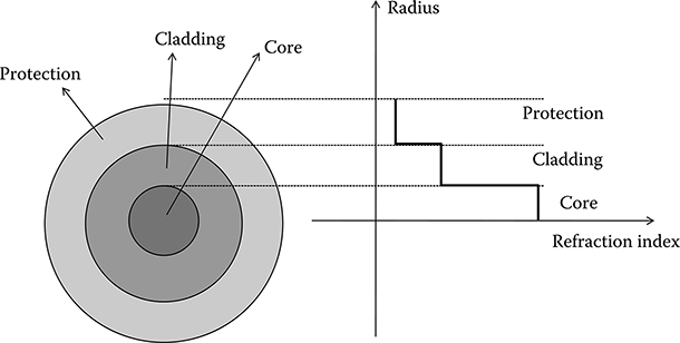
FIGURE 4.1 Section and refraction index distribution of an optical fiber.
→E=→Aζ,l,m(ρ)ei[β(ω)z−ωt](4.1)
![]()
(4.1)
where
ρ represents the radial coordinate in the fiber section
β(ω) is the dispersion function, that is obviously mode dependent z is the axial coordinate
The individual propagation mode can be identified through one of the three mode classes, represented by the footer ζ in Equation 4.1 and by two progressive numbers: l and m.
The mode classes are generally indicated as follows:
Transverse Electrical (TE) modes, having the electrical field vector “transverse,” thus orthogonal to the fiber section radius
Transverse magnetic (TM) modes, having the magnetic field vector “transverse,” thus orthogonal to the fiber section radius
HE modes, where no field is “transverse”
The propagation description through the modes represented in Equation 4.1 is accurate, but difficult to manage for our purpose.
In order to work with a simpler mode set, the solution of Maxwell equations in an orthogonal coordinate system can be attempted [3].
By exploiting again the weakly guiding property of the fiber, two sets of modes can be derived that due to the adopted coordinate system are linearly polarized (LP).
These modes (called LP) can be divided, looking at the electrical field, into x-polarized and y-polarized modes, where x and y are the orthogonal coordinates in the plane of the fiber section and due to the fiber cylindrical symmetry, every x-polarized mode is degenerate with a y-polarized mode.
Naturally, as far as the adopted approximations are valid, LP modes can be represented as a sum of TE, TM, and HE modes.
An LP mode, having, for example, linear polarization along the x axis, can be represented with the expression
→E=Al,m(ρ)ei[β(ω)z−ωt]→x(4.2)
![]()
(4.2)
where
→x![]() is the axis unitary vector
is the axis unitary vector
l,m are the mode identification numbers
LP modes are much easier to use when the fiber propagation has to be considered for telecommunication purposes.
The description of fiber propagation via LP modes is less accurate than via TE, TM, and HE modes with the effect that LP modes with the same mode index are not exactly orthogonal in real fibers, but a coupling exists.
However, in studying fiber propagation, many other approximations are done (e.g., linear fiber axis, perfect circular section, abrupt index change between the core, and the cladding) that creates much more modes coupling both among LP and among TE, HE, and TM modes, so that the LP approximation can be adopted without any problem.
Different, nondegenerate modes propagate along the fiber with different group velocities due to the dependence of the function β(ω) appearing in Equation 4.2 from the mode numbers.
The dependence of β(ω) on the propagation mode (called mode dispersion [2]) generates signal distortion when transmitting a plurality of modes and greatly limits the possible span of a transmission system.
Even if a single LP mode is excited at the fiber input, the presence of material imperfections excites all the modes that can propagate through the fiber, thus causing multimodal propagation.
In order to solve this problem, a single-mode fiber has to be designed, that is, a fiber having only one mode that propagates at the minimum attenuation wavelength.
As in any kind of waveguide, modes propagating in an optical fiber are characterized by the so-called cutoff frequency, that is, the minimum frequency at which the mode can propagate. At lower frequencies, the mode propagation is impossible since the field rapidly vanishes advancing along the fiber, irradiating the greater part of the optical power out of the waveguide.
The mode cutoff is generally expressed in terms of normalized frequency V, defined as
V=2πaλ√n2(0)−n2(∞)=acω√n2(0)−n2(∞)(4.3)
![]()
(4.3)
where
a is the core diameter
c is the light speed in vacuum
λ is the field wavelength
ω is the field angular frequency
It is assumed that the diffraction index n(ρ) is a decreasing function of the radial coordinate ρ so that n(0) is the index at the core center and n(∞) is the index of the cladding far from the core.
At each fiber mode, a cutoff normalized frequency Vc can be associated, but to LP01 modes whose cutoff is zero. That means that these two polarization degenerate modes propagate at every frequency.
The cutoff frequency of the lower cutoff mode depends on the index profile; for a step index fiber with the indexes given in Figure 4.1, the mode with the lower cutoff is the LP11 and Vc = 2.405, corresponding to a wavelength of 1262 nm for nc = 1.4600, ne = 1.4592, and the core radius equal to 10 μm. This means that, at 1300 and 1500 nm (the wavelengths at which the fiber loss is minimum), the only modes that can propagate are the LP01.
4.2.2 Fiber Losses
We have seen that the primary reason for the success of optical fiber as communication medium is the extremely low loss. Thus, studying loss mechanisms is very important.
When the light is injected into the fiber from an external light source and propagates along the fiber for a long span, the output light power is reduced with respect to the source emitted power by two kinds of losses: coupling losses and propagation losses.
Coupling losses are due to the fact that the field shape of the incoming light on the input fiber facet does not coincide with the fundamental mode profile, so that both radiation modes and below-threshold propagation modes are excited. After a very short fiber length only the fundamental mode remains, and all the power coupled with other modes is radiated out of the fiber core.
During propagation along the fiber, the fundamental mode power also decreases, due to propagation losses, to produce at the fiber output the attenuated output power.
4.2.2.1 Coupling Losses
Generally in a transmission system, light is injected into a single-mode fiber from a single-mode semiconductor laser source [4,5]. We will see dealing with lasers that the section of the waveguide composing the active region of a single-mode semiconductor laser is quite smaller than the section of a fiber (reference dimensions are 1 μm × 100 nm for the square section active waveguide of a laser versus a diameter of 10 μm for the fiber core). In this condition, a focusing system is needed to achieve good light injection into the fiber.
The focus system can be designed to focus the laser beam at the center of the input facet of the fiber. In this condition, light injection is performed as from a point source.
Since a point source emits a spherical wave, the coupling between the injected field and the suitably normalized fundamental modes is given by
η=∬→Es(ϕ,θ)·[LP0,1(φ−ϕ,ϑ−θ)→x+LP1,0(φ−ϕ,ϑ−θ)→ydϕdθ](4.4)
![]()
(4.4)
where
→Es(φ,θ)![]() is the electrical field of a spherical wave in spherical coordinates on the points of the fiber input facet
is the electrical field of a spherical wave in spherical coordinates on the points of the fiber input facet
· is the scalar product
→x![]() and →y
and →y![]() are the unitary axes vectors integral is extended to the fiber input facet
are the unitary axes vectors integral is extended to the fiber input facet
This is the maximum possible coupling efficiency. In practice, this value is never reached, due to misalignments of the focusing system both along the z axis (the focus is not exactly on the fiber facet) and in the x–y plane (the focus is not at the center of the facet).
Moreover, fiber defects (like nonconcentricity of core and cladding and core deviation from a perfect cylinder) also contribute to increasing the coupling losses.
Considering coupling of a standard step index fiber with a distributed feedback laser, practical values from 1.5–3 dB are achieved, depending on the complexity and on the tolerance of the focusing lenses and of the assembly process.
4.2.2.2 Propagation Losses
Ideally, the fundamental mode does not attenuate during transmission along the fiber. In a real fiber however, there are several mechanisms causing power attenuation. All the loss mechanisms are wavelength dependent and the final fiber attenuation is obtained by their superposition.
The first loss mechanism is the photon absorption. The absorption can be divided into intrinsic absorption and extrinsic absorption.
Intrinsic absorption is due to the characteristics of the glass composing the fiber. If no impurities were present in the fiber material, all absorption would be intrinsic.
Since the glass is an amorphous and isotopic material, it can be described as a disordered ensemble of microcrystal structures. Thus, local phonons [6] can be introduced, which models with a good approximation microcrystals vibrations related to the glass temperature.
Local phonons can be excited by the photons of the propagating radiation, thus causing photons absorption that is efficient in the infrared region and increases increasing the wavelength.
Moreover, the propagating photons can be also absorbed by the external electrons of the glass molecules, promoting them to higher energy levels. This mechanism called electron absorption, is efficient in the ultraviolet region and decreases increasing the wavelength.
Besides intrinsic absorption, impurities in the glass composition cause extrinsic absorption. In the infrared region of interest for fiber optics communication, extrinsic absorption is mainly due to metal impurities and to hydroxyl ions. These last elements in particular cause two absorption peaks to appear in the near infrared that have a great importance in determining wavelength windows for fiber communications.
Besides absorption, another important loss element is light scattering, that is, the phenomenon causing a change of photons momentum and consequently their jump from the fundamental mode to a mode that does not propagate along the fiber.
At low propagating powers, linear scattering is prevalent. In this case, no wavelength change exists between the incident photon and the scattered photon for each scattering process and the scattered photons are lost generally for radiation.
Linear scattering can be studied introducing a parameter called scattering scale and defined as
ς=πdpλ(4.5)
![]()
(4.5)
where dp is the diameter of the typical scattering particle.
If ς ≪ 1, then we are in the presence of Rayleigh scattering, if ς ≈ 1, we are in the presence of Meie scattering.
The prevalent form of scattering is the Rayleigh scattering, caused by particles and imperfections much smaller than the propagating field wavelength. Rayleigh scattering occurs with silica molecules composing the glass and it is greatly enhanced due to micro-defects that are present in the fiber material [7].
Rayleigh scattering introduces an attenuation that decreases with the wavelength.
Finally, fiber imperfections such as imperfect concentricity of core and cladding introduce another loss factor in the field propagation.
In order to analytically express the behavior of attenuation versus the field wavelength, we will define the attenuation through the attenuation parameter α defined in such a way that, if L is the fiber length, P0 the power coupled at the input with the fundamental mode, and P1 the output power, it is
P1=P0e−αL(4.6)
![]()
(4.6)
Frequently, the fiber loss is also characterized by the attenuation for a kilometer of fiber, measured in dB/km. The two parameters are directly related as can be easily derived.
A typical measure of the attenuation parameter of a step index fiber is reported in Figure 4.2, where the different contributions are also evidenced.
From the figure, it results that in a standard fiber, the low attenuation zone is divided into two parts by the hydroxyl absorption peak: a zone around 1.3 μm and a zone around 1.5 μm. For historical reasons, the two zones are called second and third transmission windows.

FIGURE 4.2 Loss contributions and total loss versus wavelength in an SSMF for signal transmission.
For a few applications, the hydroxyl (OH) absorption peaks are particularly problematic. In this case, the so-called zero water fibers can be used, where the hydroxyl ion content is so rigorously controlled that the correspondent absorption peaks are eliminated.
4.2.3 linear Propagation in an Optical Fiber
In a real fiber, attenuation is not the only phenomenon causing the difference between the field coupled at the fiber input and the field emerging from the output.
In this section, we will assume that the power of the coupled field is sufficiently low that all propagation nonlinear effects are negligible. In this hypothesis, propagation along the fiber is purely linear and the fiber itself can be modeled as a linear distributed system.
In this condition, if the field coupled to the fiber at the input facet is a combination of the two main fiber modes, then
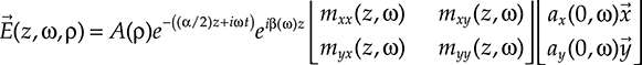
→E(0,ω,ρ)=A(ρ)[ax(0,ω)→x+ay(0,ω)→y]e−iωt(4.7)
![]()
(4.7)
The field at the output will be obtained by the multiplication of the input field in the frequency domain with the frequency transfer function of the fiber.
In real fibers factors breaking fundamental modes degeneracy in terms of the transverse field shape are present, but are not important for telecommunication systems. Thus, we can assume that the transverse shape of the field remains equal to A(ρ) in every fiber section and for every field polarization.
We have also seen that the field attenuation is a slowly varying function of the field frequency. For practical modulation, even at 100 Gbit/s, the attenuation variation in the signal bandwidth is completely negligible; thus, in writing the fiber transfer function we can assume a constant attenuation.
Fiber nonideality influences greatly the field phase evolution. As a matter of fact, in a real fiber it is not possible to assume that the propagation constants of the two LP fundamental modes are equal and that these modes do not couple during propagation.
On the contrary, the propagation constant depends on the field polarization and if a mix of the two fundamental modes is injected into the fiber, they will couple during propagation generating in every fiber section a different elliptical polarization.
Last but not least, microscopic imperfections cause coupling between the fundamental modes so that even if only one fundamental mode is launched into the fiber, that is the input field is perfectly LP, at the output, the field has a generic elliptic polarization revealing the excitation of both the fundamental modes.
Moreover, the output polarization will vary slowly in time, due to time variation of the coupling coefficient driven by phenomena like temperature and material stress variation.
These empirical observations can be summarized in the following expression of the field at a generic fiber section
→E(z,ω,ρ)=A(ρ)e−((α/2)z+iωt)eiβ(ω)z⌊mxx(z,ω)mxy(z,ω)myx(z,ω)myy(z,ω)⌋⌊ax(0,ω)→xay(0,ω)→y⌋(4.8)
(4.8)
where the matrix
[M]=⌊mxx(z,ω)mxy(z,ω)myx(z,ω)myy(z,ω)⌋(4.9)
(4.9)
called Jones matrix, has to be unitary to fulfill energy conservation and represents both birefringence (i.e., the dependence of the propagation constant from the polarization) and mode coupling (through the off diagonal coefficients). It is to be noted that, since α represents the power attenuation, α/2 appears in the field expression.
Equation 4.8 summarizes all the propagation effects characterizing the linear propagation regime in case of limited signal bandwidth.
4.2.4 Fiber Chromatic Dispersion
Chromatic dispersion in single-mode fibers is the phenomenon causing the broadening of a light pulse propagating along the fiber that is independent from the pulse polarization.
In Equation 4.8, chromatic dispersion is caused by the dependence on the angular frequency of the common mode propagation constant β(ω).
In particular, remembering the small signal bandwidth hypothesis and indicating with ω0 the central angular frequency of the signal spectrum, we can write
β(ω)≈β(ωo)+β′(ωo)(ω−ωo)+β′′(ωo)2(ω−ωo)2+β′′′(ωo)6(ω−ωo)3+...(4.10)
![]()
(4.10)
The terms of the Taylor series of β(ω) have different physical meanings.
The term β′(ω 0)z that is obtained substituting Equation 4.10 in Equation 4.8 represents a group delay, as can be easily shown from the property of the Fourier integral. This is the average delay a pulse experiments traversing the fiber span (as a matter of fact it has also the dimension of a time interval). To evidence this meaning, the time delay τ can be written as being vg = 1/β′(ω0) the group velocity.
τ=β′(ωo)z=zvg(4.11)
![]()
(4.11)
In a first approximation, injecting in the fiber a pulse with bandwidth Δω, the pulse broadening Δt can be evaluated by the group velocity dispersion (GVD) between the frequencies at the spectrum borders. Using Equation 4.10 up to the second order, the following expression is obtained.
Δτ=dτdωΔω≈β′′(ωo)Δωz(4.12)
![]()
(4.12)
Alternatively, considering wavelengths instead that angular frequencies
Δτ=dτdλdλ≈2πcλ2β′′(λ0)Δλz=DzΔλ(4.13)
![]()
(4.13)
The parameter D = 2πc/λ2β″(λ0) is called the fiber dispersion parameter (measured in ps/nm/km).
There are fundamentally two phenomena contributing to the value of the parameter D: material dispersion and waveguide dispersion, so that D can be written as the sum of a material dispersion term DM, a waveguide dispersion term DW, and a mixed term DMW, that in typical fibers is much smaller with respect to the other two.
Accurate expressions of the three terms are obtained as a result of the propagation modal analysis; here we will introduce approximated expressions for the material and guide terms in order to analyze their behavior with respect to the main fiber parameters.
The material term is related to the wavelength dependence of the silica refraction index; thus, it is the same term causing dispersion in bulk silica. It is positive, independently from the structure and design of the fiber.
In order to derive an approximated expression of this term, the propagating wave front can be approximated as a plane. The differential delay between two frequency components of the field can be written as a function of the frequency dependent group velocity as
Δτ≈L⌊1vg(ω)−1vg(ω+Δω)⌋=L[(dβdω)ω−(dβdω)ω+Δω]=β′′(ω)ΔωL(4.14)
(4.14)
The expression of the propagation constant in bulk material in the case of a plane wave is simply β(ω) = ω n(ω)/c. Substituting this expression in (4.14) and considering that in the near infrared region that is of interest for telecommunication, the angular frequency is on the order of 1015, it results as
ΔτΔω=L[ωcd2ndω2+2cdndω]≈Lωcd2ndω2(4.15)

(4.15)
From (4.15) and the dispersion parameter definition, passing from ω to λ, the following expression is obtained.
DM=−λcd2ndλ2(4.16)
![]()
(4.16)
The material dispersion, as it results from Equation 4.16 and the measured behavior of silica refraction index, is zero at a wavelength of 1300 nm, positive at longer wavelength, and negative at shorter once. In any case, DM increases while increasing λ in all the near infrared region.
The waveguide term is due to the fact that the guided mode travels part in the core and part in the cladding. Considering the case of a step index fiber, if we analyze the distribution of optical power at different frequencies we found that it depends critically on the ratio a/λ due to the different effect of the core–cladding interface diffraction on waves with different wavelength.
This effect can also be represented by studying the dependence of the effective refraction index ne (i.e., the ratio between the group velocity of a monochromatic guided wave and the velocity of light in vacuum) on the wavelength.
In particular, at short wavelengths, the effects of diffraction are smaller and the light is confined well within the core. In this condition, ne is very close to the refractive index of the core.
As the wavelength increases, the effects of diffraction become more important and the light spreads slightly into the cladding. The effective refractive index decreases toward the refractive index of the cladding.
Finally, at long wavelengths, the effects of diffraction dominate and the light in the fiber spreads well into the cladding, ne being very close to the refractive index of the cladding.
In order to obtain an approximate expression of the waveguide dispersion parameter, we will assume a zero material dispersion, a condition that can be realized only if the refraction index does not depend on wavelength. In this condition, it is useful to substitute the angular frequency with the normalized frequency V defined in Equation 4.3 that is directly related to the guiding properties of the fiber.
Thus, it is possible to write
β′(ω0)=1vg=dβdVdVdω=ac√n2(0)−n2(∞)dβdV(4.17)
(4.17)
Substituting (4.17) in the definition of the dispersion parameter it results, after expressing DW as a function of λ
DW=ddλ(1vg)=−v22πcd2βdV2(4.18)

(4.18)
The shape of the propagation constant in an ideal dielectric waveguide whose refraction index distribution does not depend on the wavelength can be varied widely by shaping the index profile being in particular either positive or negative. For example, in a step index fiber, there are two wavelength intervals: one in which the two dispersion terms are cumulative, the other in which they have different signs and one tends to compensate the other.
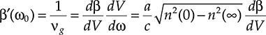
FIGURE 4.3 Dispersion contributions and total dispersion versus wavelength in a standard SSMF single-mode fiber for signal transmission.
This effect is shown in Figure 4.3 in the case of a step index fiber. In the figure, both the overall dispersion and the individual contributions are shown, evidencing the zero dispersion point (around 1.33 μm) where the two dispersion contributions are opposite.
The zero dispersion wavelength divides the wavelength axis in two intervals, that for historical reasons take the name of normal dispersion wavelengths (β″ > 0) and anomalous dispersion wavelengths (β″ < 0).
The dispersion parameter takes into account the greater contribution to fiber dispersion, but there are several cases in which the other terms of Equation 4.10 cannot be neglected. The most important of these cases is propagation around the zero dispersion frequency.
In this case, dispersion is almost all due to the third-order term, which at high transmission speed cannot be neglected.
As in the case of second-order dispersion, also in the third-order case, the pulse broadening can be approximately expressed as a linear function of the square signal bandwidth, thus defining a third-order dispersion coefficient.
In particular, the following equation is obtained:
D3=−2πcλ2β′′′(λo)(ps/nm2/km)(4.19)
![]()
(4.19)
The dispersion-related parameters of a standard step index fiber in the second and the third transmission window are reported in Table 4.1.
The fact that waveguide dispersion can be opposite in sign with respect to material dispersion can be used to shape the fiber dispersion curve. To control waveguide dispersion, the refraction index behavior along the fiber diameter is suitably designed.
Depending on the application, different types of dispersion-managed optical fibers can be used. Dispersion-shifted (DS) fibers are designed to move the zero dispersion point from the second to the third transmission window, dispersion flattened fibers are engineered to have a very low (but nonzero) dispersion in a wide wavelength interval, possibly including both second and third transmission window, nonzero dispersion fibers are generally realized to move the zero dispersion wavelength in between the two transmission windows.
TABLE 4.1 Typical Values of the Parameters of a Step Index Single-Mode Transmission Fiber
All values are at λ = 1.55 μm.
Different index profiles corresponding to different categories of fibers for long-haul transmission manufactured by the main fiber vendors are represented in Figure 4.4.
In all the cases represented in the figure, the study of the structure-guided modes demonstrate that two degenerate fundamental modes of the LP type can propagate in the fiber and that the spatial profile of this mode is Gaussian with a good approximation, exactly as in a step index fiber. The variance of the field mode shape is different for different fibers causing a difference in the field confinement. As we will see, this will have an impact on the efficiency of nonlinear effects during field propagation.
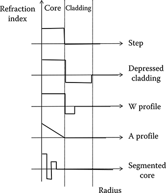
FIGURE 4.4 Different possible refraction index profiles for dispersion managed fibers.

FIGURE 4.5 Dispersion characteristic versus wavelength for different dispersion-managed fibers.
The dispersion curve of a set of “managed dispersion” fibers is reported in Figure 4.5, and some important parameters of commercial fibers are summarized in Table 4.2.
The various performances are compared with the performances of a standard step index fiber.
The first dispersion-managed fibers to be produced were DS fibers, where the dispersion curve is shifted toward higher wavelengths so that the zero dispersion wavelength is moved around 1.5 μm.
These fibers were designed and deployed in the period in which long-haul single- channel systems were designed in order to decrease chromatic dispersion and increase the transmission reach.
With the introduction of dense wavelength division multiplexing (DWDM) systems, this class of fibers was practically abandoned, due to the fact that having the zero dispersion wavelength in the third transmission window causes the maximization of nonlinear channel crosstalk due to the channel phase matching.
In order to allow high channel count DWDM systems to be deployed and contemporary to decrease as much as possible the value of dispersion, nonzero dispersion fibers were designed.
Table 4.2 Comparison between the Properties of a Set of Fibers with Different Index Profiles

All values in the table that depend on wavelength are reported at λ = 1.55 μm.
In this kind of fibers, the dispersion curve is shifted to move the zero dispersion wavelength either in between the second and the third window or beyond the third window around 1570 nm.
In the first case, the fibers are called NZ+ and in the second NZ−.
Using these fibers allows avoiding zero dispersion in the transmission bandwidth while reducing the average dispersion.
Moreover, especially in the case of NZ−, the fiber design can be performed to achieve a greater effective mode ratio to decrease nonlinear effects. This point will be considered in more detail describing nonlinear propagation.
4.2.5 Polarization Mode Dispersion
Polarization mode dispersion (PMD) is the phenomenon causing strong coupling between the fundamental LP modes so that the propagating field polarization evolves during propagation [8,9].
The polarization not only changes from fiber section to fiber section, but also changes in time and wavelength. This is due to the fact that mode coupling is generated by fiber imperfection both at the material level and at a fiber form level. While temperature and mechanical conditions like micro-stresses evolve, mode coupling changes.
The fact that the field polarization changes with wavelength is particularly dangerous for modulated signals when the field polarization has to be recovered at the receiver. As a matter of fact, this becomes impossible if different frequencies of the signal spectrum have different polarizations.
Moreover, since the diagonal terms of the Jones matrix are not equal to one, different polarizations travel through the fiber at slightly different group velocities, thus causing the so-called polarization dispersion. This means that a pulse of finite duration sent into the fiber experiments a widening during propagation even in the absence of chromatic dispersion due to the PMD.
The base for the analysis of PMD impact is the definition of the principal states of polarization (PSPs), which for a fiber with small random birefringence somehow take the place of the birefringence axes in a high birefringence medium.
Given a fiber piece, the PSPs of that fiber in the considered deploying conditions are defined as the input states of polarization that generate at the fiber output a polarization state that does not depend on ω at the first order [8].
The PSPs can be derived directly from their definition and from the general expression Equation 4.8 of the field during linear propagation in the fiber. As a matter of fact, the definition of the PSPs implies that, at first order, their ω derivative has to be equal to zero.
Let us consider the slowly varying envelope of the field in Equation 4.8. To simplify the notation, it is useful to eliminate on both sides of Equation 4.8 the transversal field shape and to write
k(ω)=−α2z+iβ(ω)z(4.20)
![]()
(4.20)
⌊ax(0,ω)→xay(0,ω)→y⌋=a(ω)eiϕ(ω)→p(4.21)

(4.21)
where →p![]() is the polarization vector.
is the polarization vector.
If the input field is a PSP, by definition the first-order derivative of the output field has to be zero. Deriving Equation 4.8 and equaling the result to zero, the following equation is obtained:
d⌊M(ω)⌋dω→p=ih(ω)[M(ω)]→p(4.22)
![]()
(4.22)
where
h(ω)=dφdω+i{dkdω−1adadω}(4.23)
![]()
(4.23)
Taking into account that the Jones matrix is unitary, it is easy to recognize that Equation 4.22 always has two solutions, which are the fiber PSPs and whose coordinate expression is easy to evaluate solving Equation 4.22.
This procedure demonstrates that, for a given fiber piece, there exist two orthogonal input polarization states, called PSPs that characterize the polarization behavior of the fiber. In particular, if a field is launched into the fiber along one of the PSPs, the output polarization does not change, at least at first order, changing ω. This means that a finite duration pulse injected in the fiber along a PSPs does not experiment widening due to PMD.
Since a higher-order dependence of the PSP output polarization on the angular frequency exists, if the bandwidth of the input signal rises above a certain value, the PSP output polarization is no more ω independent and the concept of PSPs becomes quite useless.
The PSPs bandwidth is generally on the order of 100 GHz [10]; thus, it is quite larger than the bandwidth of normal modulated signals, but for modulation at 100 Gbit/s. In this case, if pure on–off modulation is used, PSPs probably cannot be used and some other means have to be adopted to describe polarization evolution.
Even if the PSP approximation can be used, the expression of the PSPs depends on the elements of the Jones matrix and thus slowly changes with time due to the change of the random birefringence [11].
Last but not least, macroscopically identical pieces of fiber can have completely different PSPs, due to the different distribution of micro-defects causing coupling between the fundamental modes.
Starting from the PSPs definition, the PMD characteristics can be derived.
Let us call →p+![]() and →p−
and →p−![]() the unit vectors corresponding to the PSPs output polarizations of the considered fiber piece. A generic field injected into the fiber can be decomposed along the input PSPs so that, for the properties of the PSPs, the same decomposition holds for the output field with respect to the output PSPs.
the unit vectors corresponding to the PSPs output polarizations of the considered fiber piece. A generic field injected into the fiber can be decomposed along the input PSPs so that, for the properties of the PSPs, the same decomposition holds for the output field with respect to the output PSPs.
This decomposition can be written in general as follows:
→Eout=E0+sin(θ)eiφ→p++E0−cos(θ)eiΨ→p(4.24)
![]()
(4.24)
Starting from Equation 4.24, it is possible to evaluate the polarization dispersion contribution with a simple derivation exploiting the PSPs properties [12].
Squaring Equation 4.24 and remembering that the PSPs are orthogonal states, the following equation is obtained for the pulse envelope:
g(t)=g+(t)sin2(θ)+g−(t)cos2(θ)(4.25)
![]()
(4.25)
where the envelopes g+(t) and g−(t) are both replicas of the input pulse envelope that arrive at the output with different delays due to their travel along the two different PSPs.
Taking into account this consideration, we can imagine the propagation of two identical pulses launched through the fiber along the input linear polarization of the LP states.
The output envelope in the two cases can be written as in Equation 4.25 with the suitable coefficients obtaining
g1(t)=g(t−τ+)sin2(θ)+g(t−τ−)cos2(θ)g2(t)=g(t−τ−)sin2(θ)+g(t−τ+)cos2(θ)(4.26)

(4.26)
where τ– and τ+ are the delays of the PSPs.
The differential delay due to PMD is by definition the time interval separating the instants in which the peaks of two identical pulses launched in the fiber along the LP fundamental states arrive at the fiber output.
Since Equation 4.25 simply gives the expressions of the output pulses envelopes, this can be the starting point for the PMD differential delay calculation.
For a finite duration pulse, it is possible to define the moment generating function and the general theory of the Fourier transform tells us that the abscissa of the pulse maximum (that in our model is the required arrival time) is given by –iG′(0) if G(ω) is the moment generating function of its envelope, while the pulse variance is iG″(0).
Thus, the differential delay can be written as
|τ1−τ2|=|iG′2(0)−iG′1(0)|=|(τ+−τ−)cos(2θ)|(4.27)
![]()
(4.27)
From Equation 4.27, it is evident that the delay is maximum for θ = 0, that is, if the input pulses are launched along the PSPs, while it is minimum if the states along which the two input pulses are launched are inclined of π/4 with respect to the PSPs. In this case, both the input pulses are equally distributed among the PSPs and no differential delay exists.
The pulse spreading due to PMD can be evaluated starting from the definition
σΔτ=√σ2out−σ2input=√i[G′′input(0)−G′′output(0)](4.28)
![]()
(4.28)
Exploiting the properties of the moment generating function and starting from (4.26), the following expression is found for the pulse spreading:
σΔτ=12|(τ+−τ−)sin(2θ)|(4.29)
![]()
(4.29)
Equation 4.29 confirms the fact that, if θ = 0, that is, the input pulse is launched along a PSP, the pulse spreading is zero, while it is maximum if the pulse energy is equally divided between the PSPs at the fiber input.
Equation 4.29, even if it gives a very insightful expression of the pulse spreading, does not permit immediately to evaluate it starting from fiber parameters.
However, the evaluation of the average value of the pulse spread during propagation along a PMD-affected fiber can be carried out starting from Equation 4.29 with a further step.
We can imagine that the fiber link can be decomposed in several fiber pieces, each of which is completely independent from the others from a PSP point of view.
Since the output PSPs of the jth fiber piece are completely independent from the input PSPs of the (j + 1)th, the final pulse broadening is the sum of a great number of independent contributions. We can consider the average pulse spreading given by Equation 4.29 also as the time delay standard deviation, due to the fact that in the presence of PMD the time delay experienced by a pulse during the propagation along a fiber piece is a random variable.
Thus, since the variance of a sum of independent random variables is the sum of the variances, the square of the pulse broadenings experienced by the pulse while traveling along each fiber piece can be added to derive the square of the final pulse spreading, obtaining
σΔτ=12√Σj(τ+j−τ−j)sin2(2θj)(4.30)
![]()
(4.30)
where j is the index running over the different cascaded pieces of fiber. Since the injection angle is completely independent from the delay difference, the average of the product can be calculated as the product of the average.
Assuming the injection angle is uniformly distributed, in the limit of infinite pieces of negligible length, the variance of the delay difference between the PSPs is proportional to √N![]() , where N is the number of fiber pieces.
, where N is the number of fiber pieces.
Thus, if we have to evaluate the pulse broadening for a certain fiber length L, we have to multiply and divide for the square of the length of the single piece lj of fiber and make the limit N → ∞ and lj → 0 in such a way that N lj → L. By calculating the limit the following relation is obtained
σΔτ=DPMD√L(4.31)
![]()
(4.31)
where the DPMD is the PMD parameter and it is evident that, due to its statistical nature the pulse broadening due to PMD increases with the square root of the fiber length.
The same result can be derived from a statistical approach on the Jones matrix (or on the equivalent representation in the Stokes space).
A statistical polarization dispersion theory has been carried out both in the Jones and in the Stokes space [13,14] and a very elegant relationship has been developed between the two approaches based on the use of the σ spin matrixes [15].
The rigorous statistical theory arrives at the conclusion that, considering a very large ensemble of macroscopically identical fibers, the PSPs of every fiber piece are different. A statistical average of the delay can be done considering the link as a cascade of a large number of identical pieces and studying polarization evolution in this case.
The propagation along one piece of fiber generates a dispersion given by Equation 4.29, while the overall propagation, can be viewed as a random walk [14,15].
Due to the properties of the random walk, the standard deviation of the propagation time depends on the square root of the number of jumps. Since the jumps are equally probable in every fiber piece, depending on the probability on the fiber length L, the average pulse broadening σΔτ, evaluated as time delay standard deviation, is given exactly by Equation 4.31.
4.2.6 Nonlinear Propagation in Optical Fibers
Even if the optical power launched in a fiber transmission system is not huge, the core radius is so small that it is not difficult to generate so high fields that they change the equilibrium of the dielectric composing the fiber [6,7].
In this case, the constants describing the material characteristics in the wave equation depend on the field, and nonlinear effects appear.
Nonlinear propagation effects can be divided in two categories: scattering effect and the Kerr effect.
Scattering effect includes the phenomena in which a propagating field photon is scattered by some material alteration caused by the field itself.
Kerr effect includes all the phenomena due to the dependence of the real part of dielectric susceptibility on the field.
Both the classes of effects are important in telecommunication systems, because they are either exploited to improve the system performance or avoided to avoid a too high system penalty.
The starting point for the propagation problem is always the wave equation with the boundary conditions corresponding to the fiber structure.
In particular, indicating with →P(→E)![]() the polarization vector of the glass composing the fiber, the wave equation writes [16]
the polarization vector of the glass composing the fiber, the wave equation writes [16]
∇2→E−1c2∂2→E∂t2=−μ0∂2→P(→E)∂t2(4.32)

(4.32)
where →P(→E)![]() is the polarization vector.
is the polarization vector.
In a nonlinear propagation regime, the polarization is not proportional to the field, but it depends on the field in a more complex way. The consequence of this more complex dependence is the presence of wavelengths in the output signal that were not present in the input signal.
If the more powerful of these nonlinear products is much smaller than the linear component (i.e., the signal power remaining along propagation in the input bandwidth) the propagation regime is told to be weakly nonlinear. In the weak nonlinear propagation regime a few approximations can be used that simplify the problem.
In normal propagation conditions, the impact of nonlinear propagation can be classified into three main effects:
Brillouin effect: It is caused by photons scattering from coherent phonons. This is a backscattering effect.
Raman effect: It is caused by photon scattering from glass molecules in an excited state.
Kerr effect: It is caused by incoherent interaction between molecules’ external orbitals and the traveling field.
In order to set up a mathematical model of nonlinear propagation, an expression has to be adopted for the nonlinear polarization.
Assuming to be in the weak nonlinear propagation regime, series approximation of the nonlinear susceptibility can be adopted.
In general, the relationship between the susceptibility and the field is not a local and instantaneous relationship, due to the presence of distributed interactions as in the case of the Brillouin scattering. In similar cases, the susceptibility depends on the field not only in a single point and in a single instant, but incorporates a dependence extended to a finite area and to a finite time interval.
Formally, this property can be coded in mathematical terms considering the polarization vector as a convolution between the nonlinear susceptibility and the field [17], but the resulting integral–differential wave equation is really difficult to manage.
For this reason, we will assume that all fiber nonlinearities are characterized by a scalar nonlinear susceptibility. We know that in this way we will have a unified theory of Kerr and Raman effect, but we will be unable to describe Brillouin effect. For this last case, an ad hoc model will be developed.
In the local and instantaneous approximation, the Taylor series of the polarization reads
→P(→E)≈εo{χ(1)→E+→E*[χ(2)]→E+→E*[χ(3)]→E→E+...}(4.33)
![]()
(4.33)
but for χ(1) that represents the linear susceptibility, the generic term [χ(k)] of the power expansion is an Euclidean tensor with rank k + 1 so that the generic term results to be a vector, whose components are forms of degree k in the electric field components.
In particular, since the glass composing the fiber is an isotropic medium at molecular level, it can be demonstrated that [χ(2)] = 0; thus, the nonlinear propagation is mainly due to the third term of the expansion (4.33) [7].
The tensor nature of χ(3) is responsible for nonlinear polarization evolution, that is, a quite weak phenomenon, but important in some kinds of long-haul systems [17] (compare Chapter 9, Ultra Long Haul 100 Gbit/s systems).
If nonlinear polarization evolution can be neglected, the third term can be simplified introducing a scalar third-order susceptibility, so that (4.33) rewrites
→P(→E)≈εo[χ(1)+χ(3)E2]→E(4.34)
![]()
(4.34)
χ(3) is a complex term, whose real part χ(3)R![]() causes the Kerr effect and whose imaginary part χ(3)I
causes the Kerr effect and whose imaginary part χ(3)I![]() causes the Raman effect. A typical value of the real part of χ(3) is reported in Table 4.1.
causes the Raman effect. A typical value of the real part of χ(3) is reported in Table 4.1.
The presence of a nonlinear part of the susceptibility implies the dependence of the refraction index on the propagating field intensity ℐ. In particular, from the definition of the diffraction index, the following equation is derived:
n(ℐ)≈n0+n2ℐ=n0+38n0χ(3)Rℐ(4.35)
![]()
(4.35)
From what we have seen up to now, it is evident that nonlinear effect is a distributed cause of modification of the input pulses and it is more and more effective increasing the transmission fiber length.
However, by increasing the transmission length, attenuation tends to decrease the nonlinear contribution to the index, which is proportional to the local field intensity. On the other hand, increasing the dimension of the mode, the peak intensity decreases and the nonlinear effect should be less effective.
It is thus intuitive that some characteristic length has to exist, depending on fiber attenuation, mode area, and launched power, such that when the transmitted signal goes beyond this characteristic length, it is so attenuated that the nonlinear effect is no more effective.
Let us define an effective length Le such that the overall optical power present along the link is equal to the injected power multiplied by the characteristic length. The definition can be converted in a simple equation for Le that reads P0 Le=∫L0P0e−αz and whose solution is
Le=1−e−αLα(4.36)
![]()
(4.36)
where L is the fiber link length. If the fiber length is much greater than 1/α, Le results to be of the order of 1/α, that is about 20 km in standard transmission fibers.
Equation 4.36 is a pure empirical definition, but provides a useful idea of what is the fiber length causing relevant nonlinear effects.
The definition does not include the mode area. In order to also include this element, It can be suitably modified starting from the definition of the mode effective area that, in the hypothesis of perfectly symmetric mode, reads:
Ae=[∬|E(ρ,φ)|2ρdφdρ]2∬|E(ρ,φ)4ρdφdρ=π[∫∞0|A(ρ)|2ρdρ]2∫∞0|A(ρ)|4ρdρ(4.37)

(4.37)
At this point, Equation 4.36 could be modified as follows:
L′e=AcAe1−e−αzα(4.38)
![]()
(4.38)
where Ac is the geometrical core area. In the case of a step index fiber with a core radius of 5.2 μm, Ac/Ae = 0.95, so that the results of Equations 4.36 and 4.38 practically do not differ. In other cases however, there is quite a difference. For example, in the case of a DS fiber with the same geometrical core radius, Ac/Ae = 0.6 clearly indicating the greater efficiency of nonlinear effects in this kind of fiber due to the greater field confinement.
However, it is the length defined by Equation 4.36 that appears in several equations regarding nonlinear effects and generally it is the quantity called characteristic length of fiber nonlinear effects.
4.2.7 Kerr Effect
Under the hypotheses set in the previous section, to analyze the impact of Kerr effect, we can neglect in a first approximation the polarization evolution and imagine dealing with ideal LP modes.
Several effects induced by the Kerr nonlinearity are much more efficient if the interacting signals polarizations are aligned so that a scalar model results to enhance the nonlinear effect with respect to the real vector case. A discussion on the applicability limits of the scalar model for the analysis of transmission systems is reported in [18].
If transmission penalties have to be evaluated, this is a reasonable approach, providing a worst case system performance, if the nonlinear effect is exploited to design some fiber-based device, the correctness of the scalar assumption has to be explicitly verified due to the risk of overestimating the device performances.
In these conditions, it is possible to derive a propagation equation in the presence of Kerr effect by applying the slowly varying approximation and considering the Kerr effect response time about zero so to deal with an instantaneous effect (being the Kerr characteristic time of the order of 100 fs this, approximation is always valid in telecommunications). This equation, called nonlinear Schrödinger equation, writes [6,19]
i∂E∂z=−iα2E+β′′2∂2E∂τ2−γ|E|2E(4.39)
![]()
(4.39)
where τ is the time in the pulse reference frame, thus τ = t − z/vg = t − β′z, and the nonlinear coefficient given by γ = n2ωk/(Cπrm2) with rm representing the modal radius.
Also within this approximation, the evolution in the presence of a wideband signal is complex and, in order to understand from a qualitative point of view the signal distortions introduced by Kerr effect, signal propagation is generally studied assuming a few simple expressions for the fiber input signal.
These particular signals are conceived to put in evidence particular aspects of the Kerr effect, aspects that are called, for historical reasons “effects.” Thus, we speak about self phase modulation (SPM) effect, cross phase modulation (XPM) effect, four wave mixing (FWM) effect, and so on. However, all these phenomena are Kerr effect–induced evolutions of particular input signals.
If the input signal is complex, the evolution can be qualitatively understood by considering the input as a superposition of a certain number of simple signals and using the fact that the nonlinear effect is small to try to model the final result as the superimposition of the effects on each simple signal (compare in Chapter 6 the rule of penalties addition and Appendix C).
This approach is quite useful to understand complex phenomena also, but has clear limits either when the power is very high and the superposition of the individual effects cannot be assumed or when the bandwidth is very large, so that parameters dependence on wavelength cannot be neglected. These conditions are not so far from the operational conditions of long-haul high-capacity WDM systems; thus, the validity of all the approximations has always to be verified when in front of a real system.
To access more quantitative results, several methods have been devised to numerically solve Equation 4.39 and their study can start from bibliographies [18,20].
4.2.7.1 Kerr-Induced Self-Phase Modulation
If an amplitude-modulated signal is injected into the fiber, the presence of nonlinear refraction index n2 causes the intensity modulation to be reflected into a phase modulation in such a way that the signal phase, in the approximation of very weak effect, writes
Φ(t)≈n0z+Φ0+2πλn2ℐ(t)z(4.40)
![]()
(4.40)
where ℐ(t) is the field intensity that is time dependent due to modulation.
In the simplest case, the presence of a sinusoidal modulation, the sidebands of the signal spectrum are unbalanced for the superposition of the amplitude modulation and phase modulation.
If a signal with a more complex amplitude modulation is injected into the fiber, SPM causes a chirp, which is a dependence of the signal phase on time, and causes a nonlinear pulse broadening.
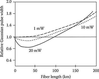
FIGURE 4.6 Broadening of a Gaussian pulse propagating in a DS fiber at 1.55 μm with zero chromatic dispersion versus the pulse power after the propagation through a variable length of fiber.
(After Chraplyvy, A.R., J. Lightwave Technol., 8, 1548, 1990.)
The broadening of a Gaussian pulse propagating in a DS fiber at 1.55 μm with zero chromatic dispersion is shown in Figure 4.6 [21] versus the pulse power after the propagation through a variable length of fiber.
It is interesting to observe that, even if for long distances the pulse is always broadened, at high transmitted power, there is a distance range where the pulse width decreases. This is due to the fact that SPM creates a phase modulation frequency distribution that on one side of the central carrier is out-of-phase with respect to the original frequency distribution that is due to the amplitude modulation. In the long run and at high powers, the nonlinear phase distribution prevails and determines the spectrum width, but a range of fiber lengths and field powers exist where the left modulation bands almost cancels, generating a pulse width decrease. This interpretation of the pulse shrink is confirmed by the fact that the minimum relative pulse width arrives near 0.5 and never goes below this value.
The SPM-induced broadening superimposes with the broadening due to fiber dispersion. In the normal dispersion regime, the two effects have the same sign and the observed pulse broadening is greater than that due to dispersion alone; on the contrary, in the anomalous regime the two effects have different signs and the overall broadening is smaller than that due to dispersion.
This effect is very important in transmission systems.
When the Kerr effect theory was consolidated, it was also discovered that, giving to the intensity of the field a particular shape, the linear and nonlinear effects completely cancel and the pulse propagates without broadening through thousands of kilometers of fiber. These particular pulses are known as solitons and in a first moment they were regarded as the key to design very high-capacity and ultra-long-haul systems [18,19,22].
The propagation dynamics of solitons however is quite complex: since a single pulse travels unchanged but for attenuation, and since the zero broadening condition is reached only for a precise value of the input power, a soliton can be realized only in a first approximation in a real fiber.
Even if a single soliton does not broaden, a random train of nearby solitons (representing a random string of bits) is affected by a sort of jitter due to the attraction between adjacent pulses. Moreover, if WDM is used, more jitter comes out due to the interaction between frequency adjacent channels.
Last but not least, perfect nonlinear and linear chirp compensation creates perfect phase matching among WDM channels belonging to the same comb, maximizing the dangerous nonlinear interchannel crosstalk.
A great amount of research has been devoted to solve these problems, producing brilliant solutions and a great insight on nonlinear propagation, but at the end, soliton systems never passed from laboratories to production, even if a great number of field tests were done.
The practical result of all this research was however the discovery that, even if mathematical solitons are too complex to be implemented in a practical system, the soliton principle can be exploited in any case.
In this way, the present day ultra-long-haul systems were born. In these systems, SPM is used to partially compensate chromatic dispersion to greatly reduce pulse broadening without creating perfect phase matching between spectrally adjacent channels.
4.2.7.2 Kerr-Induced Cross-Phase Modulation
When a comb of amplitude-modulated signals at different wavelengths is injected into the fiber, the expression of the phase of one of them becomes, in the approximation of weak nonlinear effect:
Φj(t)≈n0z+Φ0j+2πλn2zℐj(t)+4πλn2zΣk≠jℐk(t)(4.41)

(4.41)
Besides the phase modulation imposed by SPM, another phase modulation term exists due to the presence of the channels at other wavelengths. In practical cases in which different channels are quite near (e.g., at 100 GHz spacing, that in wavelength units is a spacing of about 0.84 nm around 1.55 μm), n2 is almost the same for all the channels and the weight of XPM is doubled with respect to the weight of SPM.
However, due to the time dependence of the intensity ℐk(t), XPM is effective only when the intensity of the signal under consideration and the intensity of the interfering signal are superimposed in time. In a WDM transmission, due to the frequency difference of the different channels, there is a shift of one channel with respect to the other whose speed depends on the frequency distance of the considered channels. This shift, also called walkoff, reduces the efficiency of XPM and all the effects requiring phase matching.
Moreover, the effect of chromatic dispersion also causes a shift of one channel with respect to the other due to the different group velocity, implying that higher the dispersion less efficient is the XPM.
4.2.7.3 Kerr-Induced Four-Wave Mixing
Besides XPM, when several signals at a different wavelength propagate through an optical fiber, another important nonlinear interaction is caused by the Kerr effect: the so-called FWM.
Even if FWM is also generated by a couple of propagating waves, it is a four photons phenomenon, involving, in the case of two interacting wavelengths, two photons from one wavelength and one from the other, besides a photon at a different wavelength. This different wavelength photon is generated via absorption of photons of the traveling radiation and reemission through the transition at an intermediate molecular vibration level.
Thus, the nature of the FWM is more evident imagining three different radiations at angular wavelengths ωi (i = 1, 2, 3) that travels through a fiber in the same direction.
The third-order nonlinear polarization can be obtained by substituting the expression of the overall field into Equation 4.34 and grouping the terms with the same frequency to determine the frequency components of the output spectrum.
Besides three components at the input frequencies, the output spectrum is composed of the four frequency components at the angular frequencies
ωj=ω1±ω2±ω3(4.42)
![]()
(4.42)
In spontaneous FWM, these new frequencies are created in a part of the spectrum that does not contain any radiation power at the fiber input, if on the other side a radiation is present at the FWM frequencies like in the case of WDM transmission, the FM component superimposes to the input field causing crosstalk.
At each FWM frequency, there is a corresponding term of the nonlinear glass polarization whose amplitude depends on the product of the amplitudes of the input fields and whose phase has the following expression
θj=[β(ω1)±β(ω2)±β(ω3)−β(ωj)]z−[±ω1±ω2±ω3−ωj]t(4.43)
![]()
(4.43)
The term θj is called phase matching of the jth FWM frequency and the power of the jth FWM frequency is maximum when θj is equal to zero and minimum when θ j is equal to π/2.
During the propagation through a real fiber, the phase matching for a certain FWM frequency depends on the axial coordinate z and effective generation of the new frequency happens only when the infinitesimal contributions generated in correspondence of each fiber section add together to form a sizeable optical power.
In order to have this superposition, the term depending on t in (4.43) has to vanish so that fixing selection rules for the frequencies where macroscopic FWM can be observed: they are all the frequencies where at least ωj appears with the opposite sign with respect to the other angular frequencies.
In this case, the time dependent term in the phase matching expression vanishes with a suitable choice of ωj and the phase matching condition becomes
Δβ=[β(ω1)±β(ω2)±β(ω3)−β(ωj)]=0(4.44)
![]()
(4.44)
In order to satisfy this condition, chromatic dispersion has to be negligible.
The evolution of the FWM generated waves, besides that of the waves injected at the fiber input, can be derived by solving the nonlinear wave equation. Following the method of the coupled waves equations it can be decomposed in a set of coupled wave equations, one for each wave, containing the coupling terms that derives from the nonlinear interaction.
In the so-called nondepleted pump condition, that is, when the nonlinear interaction is very low and the coupling terms in the equations describing the evolution of the injected waves can be neglected, the coupled waves equations can be analytically solved.
Assuming to have three waves at the fiber input, the power of the jth FWM wave is given by [23]
E2j(z)=2ηγ2d2eL2eE21(z)E22(z)E23(z)e−αz(4.45)
![]()
(4.45)
where
Le indicates the characteristic length defined in Equation 4.36
de is the so-called degeneracy factor that is equal to 3 in case of degenerate FWM, when two interacting photons have the same frequency, and 6 in the other cases
γ is the so-called nonlinear coefficient
η is the FWM efficiency, that is, the parameter that represents the effectiveness of the nonlinear effect
The FWM efficiency η can be written as follows [23]:
η=α2α2+Δβ2[1+4e−αzsin2(Δβz/2)(1−e−αz)2](4.46)

(4.46)
The dependence of the FWM efficiency on dispersion is clear from Equation 4.46, since Δβ cannot be equal to zero in the presence of sizable chromatic dispersion.
Approximating the propagation constants with their second-order approximation and assuming β 2 independent from the wavelength, an expression of the FWM efficiency as a function of the dispersion constant can be obtained.
The FWM efficiency in the higher-efficiency case (ω1 ≠ ω2, ω1 + ω2 − ω3 = ωj) is shown in Figure 4.7 [21] versus the spacing between adjacent injected frequencies Δω = ω1 − ω 2 = ω2 − ω3. All parameters are evaluated at 1.55 μm and two values of D are considered: 16 ps/nm/km (corresponding to a standard step index fiber) and 1 ps/nm/km (corresponding to a DS fiber).
The dependence of the efficiency from the input field spacing and on the dispersion is clear and similar plots can be used to understand the impact of FWM in WDM systems.
4.2.8 Raman Scattering
Raman scattering is the photon scattering caused by local optical phonons of the glass and in Equation 4.39 it is taken into account via the imaginary part of the third-order nonlinear susceptibility [6,7].
When a monochromatic light beam propagates in an optical fiber, spontaneous Raman scattering occurs. It transfers some of the photons to new frequencies. The scattered photons may lose energy (Stokes shift) or gain energy (anti-Stokes shift). If photons at other frequencies are already present then the probability of scattering to those frequencies is enhanced. This process is known as stimulated Raman scattering and rely on stimulated emission due to the excited optical phonons.
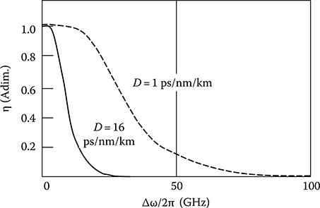
FIGURE 4.7 FWM efficiency in the higher-efficiency case (ω1 ≠ ω2, ω1 + ω2 − ω3 = ωj) versus the spacing between adjacent frequencies Δω = ω1 − ω2 = ω2 − ω3. All parameters are evaluated at 1.55 μm and two values of D are considered: 16 ps/nm/km (corresponding to a standard step index fiber) and 1 ps/nm/km (corresponding to a DS fiber).

FIGURE 4.8 Raman gain spectrum in an SSMF versus the frequency shift from the pump wavelength.
(After Shibate, N. et al., J. Non Cryst. Solids, 45, 115, 1981.)
In the Stokes scattering process, the only process happening in guided propagation due to the overall momentum conservation, the energy of incident photon is reduced to lower level and energy is transferred to the molecules of silica in the form of kinetic energy, inducing stretching, bending or rocking of the molecular bonds. The Raman shift ωR = ωP − ωS (when P indicates the injected wavelength and S the Stokes wavelength produced by the nonlinearity) is dictated by the vibrational energy levels of silica.
The Stokes Raman process is also known as the forward Raman process since the Stokes wave propagates in the same direction of the input wave and the energy conservation for the process is
εg−ħωp=εf−ħωs(4.47)
![]()
(4.47)
where εg and εf are ground state and final state energies, respectively, and in silica fiber ωP − ω S ≈ 12 THz (that in the third windows are about 100 nm).
Since Raman scattering is not only a potential cause of channel crosstalk in WDM systems, but also the principle of operation of Raman amplifiers that are used in several transmission system architectures, we will delay the discussion of a detailed physical model of the Raman amplification to the next section.
Here it is interesting to note that the gain bandwidth of the Raman effect, whose experimental measure is reported in Figure 4.8 [24], is extremely wide and that, as all nonlinear effects generate new waves, the Stokes wave has an exponential growth in the limit of nondepleted pump, when the effect is thus very low.
In correspondence to the slope change of the exponential, a Raman threshold can be defined whose value is about 600 mW in conventional standard single-mode fibers (SSMFs).
4.2.9 Brillouin Scattering
Brillouin scattering is a nonlinear process that can occur in optical fibers at large field intensity. The large intensity produces compression in the material of the core of the fiber through the process known as electrostriction. This phenomenon produces density fluctuations in the fiber medium, which in turn modulates the refractive index of the medium and results in an electrostrictive nonlinearity [25].
The modulated refractive index behaves as an index grating, which is pump-induced and the scattered light is frequency shifted (Brillouin shift) by the frequency of the sound wave.
Quantum mechanically, the Brillouin shift originates from the coherent scattering between photon and local acoustic phonon, and the Brillouin shift is due to the Doppler displacement that is a consequence of the phonon momentum [26].
Brillouin scattering may be spontaneous or stimulated. In spontaneous Brillouin scattering, there is annihilation of a pump photon, which results in creation of Stokes photon and an acoustic phonon simultaneously. The conservation laws for energy and momentum must be followed in such scattering processes. For energy conservation, the Stokes shift ωB must be equal to (ωP − ωS), where ωP and ωS are frequencies of pump and Stokes waves.
The momentum conservation requires
→kA=(→kp−→kS+j→klattice)(4.48)
![]()
(4.48)
where
→kp![]() and →kS
and →kS![]() are the pump photon and the phonon wave vectors j is an integer
are the pump photon and the phonon wave vectors j is an integer
→klattice![]() takes into account the pseudo-particle nature of the phonon and accounts for other Stokes orders after the fundamental
takes into account the pseudo-particle nature of the phonon and accounts for other Stokes orders after the fundamental
In transmission systems, Brillouin effect has to be as small as possible; thus, only the first-order Stokes wave is to be taken into account, so that Equation 4.48 can be simplified as →kA=(→kp−→kS)![]() .
.
If vA is the acoustic velocity, then the dispersion relation Equation 4.48 can be written as
ωB=vA|→kA|=vA|→kp−→kS|=2vA|→kp|sin(ϑ2)(4.49)

(4.49)
where ϑ is the angle between the pump and Stokes momentum vectors and the modules of the pump and the Stokes wave vectors are assumed almost equal due to Equation 4.48 and to the fact that the light speed is much greater than the sound speed. From the aforementioned expression, it is clear that the frequency shift depends on angle ϑ. For ϑ = 0, the shift is zero, that is, there is no frequency shift in forward direction that means no Brillouin scattering. The only other possible direction in guided propagation is ϑ = π that represents backward direction and gives the maximum shift. The backward Stokes shift can be evaluated from Equation 4.48 obtaining
ωB=4πnvAλP(4.50)
![]()
(4.50)
where n is the effective mode index, that is, the ratio between the light speed in vacuum and the mode group velocity.
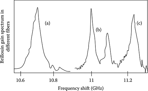
FIGURE 4.9 Brillouin gain spectra at pump wavelength 1.525 mm for a silica-core fiber (a), a depressed-cladding fiber (b), and a DS fiber (c).
(After Nikles, M. et al., J. Lightwave Technol., 15, 1842, 1997.)
The dependence of gain on frequency can be described evaluating the Brillouin gain spectrum. The finite life time TB of acoustic phonons is the cause of the frequency dependence of the gain and of the small spectral width of the gain spectrum.
Solving the coupled wave equations of the input optical wave, the Stokes wave, and the acoustic wave, the following expression can be obtained for the Brillouin gain gB
gB(ω)=gB01+(ω−ωB)2T2B(4.51)
![]()
(4.51)
The peak value of the Brillouin gain occurs at ω = ωB. The gain gB0 depends on many parameters like concentration of dopants in the fiber, inhomogeneous distribution of dopants, and the electrostrictive coefficient. Figure 4.9 describes the Brillouin gain spectra at pump wavelength 1.525 mm for a silica-core fiber, a depressed-cladding fiber, and a DS fiber.
The inhomogeneous distribution of germania within the core of the depressed-cladding fiber used for the experiment is responsible for the double peak in the Brillouin gain spectrum of the figure, while difference in Brillouin shift among various fibers is due to the different percentage of germania in the core.
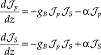
Exploiting the expression of the Brillouin gain, it is possible to develop a simple model of the evolution of the pump and Stokes wave intensities during propagation.
As a matter of fact, separating the equation for the pump and the equation for the Stokes from the general wave equation and applying the rotating wave and the slowly varying envelope approximations, the following coupled equations are obtained for the two optical waves intensities:
dℐpdz=−gBℐpℐs−αℐpdℐsdz=−gBℐpℐs+αℐs(4.52)
(4.52)
In the condition of very small nonlinear effect, the Stokes intensity can be neglected in the equation for the pump and the system (4.52) can be solved exactly.

FIGURE 4.10 Power exiting from the far end (continuous line) and the near end (dotted line) of 13 km of DS fiber versus the input power at the near end of the fiber.
Since the optical power is proportional to the optical intensity via the simple relationship ℐAe = P, where the proportionality coefficient is the effective area defined in (4.37), and since the Stokes is counter-propagating with respect to the pump, the solution for the Stokes power exiting from the fiber input facet is
PS(0)=PS(L)e−αLegB PP(0)Le/Ae(4.53)
![]()
(4.53)
From Equation 4.53, it is possible to evaluate the Brillouin threshold as the pump power at which the Stokes power at the input facet is equal to the pump power at the output facet.
Assuming PS(L) equal to the average spontaneous emission noise at the wavelength of 1.55 μm, thus representing the case of the absence of a coherent Stokes signal at the far end fiber facet and describing the pump evolution in the nondepleted pump approximation, the Brillouin threshold can be expressed as [27]
Pth=21δAegBLe(4.54)

(4.54)
The value of polarization factor δ lies between 1 and 2 depending on relative polarization of pump and Stokes waves. Typically, Ae ≈ 50 μm2, L e ≈ 20 km, and gB = 4 × 10⁻¹¹ m/W for a fiber system at 1550 nm.
With these values and taking δ = 1, Pth ≈ 1.3 mW. The threshold power becomes just double if polarization factor is taken equal to 2. When threshold is reached, the effect of stimulated Brillouin scattering (SBS) on the signal power is described by the Figure 4.10, where the power exiting from the far and the near end of 13 km of DS fiber is plotted versus the input power at the near end of the fiber. Up to the threshold power, the transmitted power increases linearly. When scattered power attains the value equal to threshold power, the transmitted power becomes almost constant and independent of input signal power.
4.2.10 ITU-T Fiber Standards
The International Standardization Organization (the ITU-T) has standardized several types of fibers to allow system designers to rely on well-known set of fiber parameters.
Table 4.3 Summary of the Main ITU-T and IEC Standards Regarding Transmission Fibers

Besides ITU-T, the most important organization that has done an extensive optical fiber standardization is International Electrotechnical Commission (IEC), whose influence is mainly present in North America.
A summary of the main recommendations of ITU-T and IEC for standardization is reported in Table 4.3.
The most common fiber in the world, deployed almost by all the carriers is the nondispersion-shifted fiber (NDSF) or G.652 fiber, also called SSMF.
This is a step index fiber optimized for low dispersion in the third windows. Even if SSMFs are the oldest among all the installed fibers, their characteristics are evolving on the push of the increasing speed of transmitted channels.
In particular, manufacturing processes are continuously improved to decrease PMD and to control the attenuation in the extreme parts of the spectrum.
Due to the relatively high value of the dispersion parameter, SSMFs allow a very good control of FWM and XPM interference in WDM systems.
Moreover, a particular class of G.652 fiber exists where the HO content in the fiber glass is so reduced that the HO attenuation peak almost disappears widening the available spectrum. This property is useful especially in coarse wavelength division multiplexing (CWDM) systems, where two of the standard channels are superimposed to the HO attenuation peak and cannot be used with SSMFs.
A few key specifications from ITU-T G.652 are reported in Table 4.4.
Second from the point of view of deployed length are the G.655 fibers. They are NZ+ and NZ− fibers, which trade a bit of attenuation with a substantially low dispersion in all the third window.
In reality, G.655 fibers have never demonstrated their capability to support 10 Gbit/s DWDM transmission systems with performance superior to that of G.652 fibers.
The continuous increase of the value of D at 1550 nm of the most recent G.655 fibers has demonstrated that the optimal trade-off between D, Ae, and α has not been found yet.
DS fibers, standardized in ITU-T recommendation G.653, have on the contrary almost disappeared from the market today.
Avoiding dispersion in single-channel transmission at 1550 nm resulted in exacerbation of both XPM and FWM. Moreover, DS fibers have a higher PMD with respect to SSMF because of the core–cladding index difference two times higher than that of G.652 fibers.
Table 4.4 A Few Key Specifications from ITU-T G.652

A few key requirements from G.653 and from G.655 are reported in Tables 4.5 and 4.6, respectively.
4.2.11 Polarization Maintaining and Other Special Telecom Fibers
A polarization maintaining (PM) fiber is an optical fiber in which if the input field is injected along a predefined linear polarization (the polarization of the only LP fundamental mode of the fiber), this polarization is maintained during propagation [28].
Several different designs of PM fiber are used. Most work by inducing stress in the core via a noncircular cladding cross section, or via rods of another material included within the cladding. Several different shapes of rods are used, and the resulting fiber design has the standardized name such as “PANDA” and “Bow-tie,” as it is shown in Figure 4.11. There are small differences between different types of PM fiber design, more in the manufacturing process than in the final product performance.
Table 4.5 A Few Key Requirements from G.653

Table 4.6 A Few Key Requirements from G.655
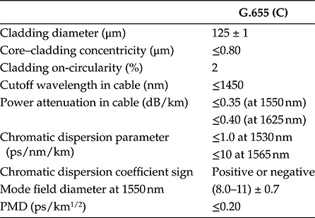
It is to underline that a PM fiber does not polarize light as a polarizer does. Rather, PM fiber maintains the input linear polarization if it is launched into the fiber along the correct direction. If the polarization of the input light is not aligned with the stress direction in the fiber, the output will vary between linear and circular polarization (and generally will be elliptically polarized).

FIGURE 4.11 Schematic cross section of different special fibers for use in telecommunication systems. Polarization maintaining and single-polarization fibers are sketched in the upper part of the figure, examples of PCFs are reported in the lower part.
Polarization maintaining fibers are generally characterized by a minimum loss greater than 1 dB/km (typical for a PANDA fiber is 1.5 dB/km) that, besides the high cost, makes them unsuitable for transmission. However, there are several applications requiring small pieces of a PM fiber, such as optical components pigtailing, fiber optic sensing, interferometry, and quantum key distribution. They are also commonly used in telecommunications for the connection between a source laser and a modulator, since the modulator requires polarized light at the input.
Single-polarization fibers [28,29] are special optical fibers that can transmit light with a certain linear polarization direction, whereas light with the other polarization directions is either not guided or experiences strong optical losses. Such fibers should not be confused with PM fibers, which guide light with any polarization state, but can preserve a linear polarization state when the polarization direction is properly aligned with the birefringence axis.
In many cases, single-polarization guidance occurs in only a limited wavelength range. Outside that range, both polarization directions or no light at all may be guided. Also, some fibers exhibit a limited extinction ratio.
Different principles of operation can be utilized for single-polarization fibers. A common approach is the use an elliptical core, which introduces strong birefringence and also a polarization dependence of a cutoff wavelength, so that only light with one polarization direction is guided, whereas the fiber is a leaky waveguide for the other polarization.
After the fibers having particular polarization properties, a great importance in the design of DWDM systems is the dispersion compensating fibers (DCFs) [30,31].
This kind of fiber is designed to have a strong dispersion in the third transmission window so that a relatively short fiber piece can compensate an entire SSMF span from 70 to 100 km.
This result is achieved by suitably shaping the refraction index in the core and in the cladding of the fiber.
A typical index shape of a DCF is the segmented core profile represented in Figure 4.4. Two figures of merit can be given for DCFs:
Efficiency (ɛ) that is dispersion divided by the dispersion slope for a standard SSMF divided by the same ratio but for the DCF.
Figure of merit (FM) that is minimum dispersion in the C band divided by maximum attenuation in C band.
Efficiencies greater than 60% and FM as high as 150 can be obtained from commercial products that are completely sufficient for the field applications in DWDM systems. For example, a DCF length having 11.5 dB of loss can compensate 1640 ns dispersion in the C band (1545–1606 nm).
Photonic crystal fibers (PCFs) [32] are another type of special fibers that could find wide application in future telecommunication system mainly in active and passive fiber devices. They are an attempt to incorporate the bandgap ideas of photonic crystals into the fiber structure by stacking periodically a regular array of channels and drawing into fiber form (see Figure 4.11).
Two classes of PCFs exist [33,34], according to their mechanism for field confinement. Those with a solid core, or a core with a higher average index than the microstructured cladding, operates on the same indexguiding principle as conventional optical fiber.
However, they can have a much higher effective refractive index contrast between core and cladding, and therefore, they can have much stronger confinement for applications in nonlinear optical devices or, polarization-maintaining fibers. Alternatively, a “photonic bandgap” fiber can be created, in which the light is confined by a photonic bandgap created by the microstructured cladding—such a bandgap, properly designed, can confine light in a lower-index core and even a hollow (air) core [35].
In general, regular structured fibers such as PCFs, have a cross section (normally uniform along the fiber length) microstructured from one, two or more materials. Most commonly, the microstructure is periodically arranged over much of the cross section, usually as a “cladding” surrounding a core where light is confined. For example, the fibers demonstrated in [36] consisted of a hexagonal lattice of air holes in a silica fiber, with a solid or hollow core at the center where light is guided. Other arrangements include concentric rings of two or more materials.
Recently, it has been recognized that the periodic structure is actually not the best solution for many applications. This idea has been applied to reduce bend losses, and for achieving structured optical fibers with propagation losses below that of the SSMF.
PCFs with different designs of the hole pattern can have very remarkable properties, strongly depending on the design details:
Single-mode guidance over very wide wavelength regions (endlessly single-mode fiber) is obtained for small ratios of hole size and hole spacing [37].
Extremely small or extremely large mode areas are possible. These lead to very strong or very weak optical nonlinearities. PCFs can be made with a low sensitivity to bend losses even for large mode areas [38].
Certain hole arrangements result in a photonic bandgap, where guidance is possible even in a hollow core, as a higher refractive index in the inner part is no longer required.
Asymmetric hole patterns can lead to extremely strong birefringence for polarization-maintaining fibers [39]. This property can also be combined with large mode areas.
Strongly polarization-dependent attenuation (polarizing fibers) [40] can be obtained in different ways. For example, there can be a polarization-dependent fundamental mode cutoff, so that the fiber guides only light with one polarization in a certain wavelength range.
Similarly, it is possible to suppress Raman scattering [41] by strongly attenuating longer-wavelength light.
Multicore designs are possible, for example, with a regular pattern of core structures in a single fiber, where there may or may not be some coupling between the cores.
In the field of telecommunications however, probably the most important application of the holey fibers is in optical amplifiers.
Laser-active PCFs for fiber lasers and amplifiers can be fabricated by using, for example, a rare-earth-doped rod as the central element of the preform assembly. Rare earth dopants (e.g., ytterbium or erbium) tend to increase the refractive index, but this can be precisely compensated, for example, with additional fluorine doping, so that the guiding properties are determined by the photonic microstructure only and not by a conventional-type refractive index difference.
Generally, PCFs are constructed by the same methods as other optical fibers: first, one constructs a “preform” on the scale of centimeters in size, and then heats the preform and draws it down to the fiber diameter, shrinking the preform cross section but maintaining the same features. In this way, kilometers of fiber can be produced from a single preform.
Most PCFs have been fabricated in silica glass, but other glasses have also been used to obtain particular optical properties (such has high optical nonlinearity). Using this principle, for example, fibers optimized to have a very high Raman efficiency have been fabricated, which are conceived for the design of high-gain low-noise Raman amplifiers.
However, special care is required in various respects:
Ends of PCFs may not be cleaned with liquid solvents, such as ethanol, as capillary forces may pull them into the holes.
Pulling very long length of microstructured fibers is not easy due to the need of maintaining the cross section constant and in general there is a limit to the length of a piece of such fibers.
Cleaving and fusion splicing PCFs is in principle possible, but can be more difficult, particularly for fibers with large air content. During fusion splicing, the air may expand and distort the fiber structure.
Connections between fibers are also possible with a variety of mechanical splices, fiber connectors, protected patch cables, beam expansion units, etc.
Even when the splicing process works well, there may be a substantial coupling loss due to a mismatch of mode areas, for example, when a small-core PCF is copled to a standard single-mode fiber. There are special tapered single-mode fibers and tapered PCFs for enhancing the coupling efficiency, but these may not be easily available.
4.2.12 Fiber Cables
Simply covered by the polymer jacket, an optical fiber is impossible to deploy in the field. In order to be used, an optical fiber has to be packaged in a fiber cable [42].
The major benefits of fiber optic cabling are as follows:
Easy handling: Some communication systems require tens or even hundreds of fibers (such as a metro backbone system). However, fibers in a cable make it very easy to install and maintain.
Protection from damaging forces: Fiber optic cables have to be pulled into place through ducts (outdoor) or conduits (indoor). Pulling eyes are attached to the strength members or cable outer jackets. This is critical for isolating the fibers from the applied pulling forces. Glass fibers cannot endure more than 0.1%–0.2% elongation during installation.
Protection from harsh environment factors: Cable structures protect fibers from moisture (outdoor cables), extreme temperature (aerial cables) and influx of hydrogen into the fiber (which causes light absorption peak at 1380 nm, which in turn impair fibers’ transmission properties).
FIGURE 4.12 Scheme of the structure of a fiber cable: (a) tight-buffered cable and (b) loose tube cable.
For current telecommunication applications, practically only single-mode fibers are used, also in the access area. Thus, all the telecommunication cables include single-mode fibers, even if multimode fiber cables and even mixed fiber cables are still used for other applications or for compatibility with legacy systems generally in the access area.
The first element in determining the characteristics of a fiber cable is the choice of materials used to package the cable.
Depending on the environment in which the cable has to be deployed, different requirements are imposed to the design and different materials have to be chosen.
For indoor cables, used for LANs or internal cabling of carriers central offices, fire safety is the number one factor. Moreover, especially in the LAN application, protection of the inner fibers against excessive bending and easy installation in the typical LAN conduit is another key requirement.
In the case of outdoor cables, moisture resistance and temperature tolerance are the major factors when choosing materials. They also need to be ultraviolet resistant and capable of sustaining the stresses related to typical installation procedures without damage.
Finally, aerial self-supporting cables must endure extreme temperature ranges from sunlight heat to freezing snow. They also must survive high wind loading.
The structure of a fiber cable, schematically reported in Figure 4.12, is designed to allow these requirements to be fulfilled.
The fibers are sustained by an internal strength member made from steel, Aramid yarn [43], or some other material with high resistance to traction and high elasticity. The role of the strength member is to give mechanical resistance to the cable and to allow cable traction during installation. When a cable is pulled into a duct, the tension is applied to the strong member instead of the fibers.
Aramid yarn (Kevlar is its commercial name that is a product trademark) is a yellow color, fiber-looking material. It is strong and is used to bundle and protect the loose tubes or fibers in the cable.
Every fiber is individually protected with a polymer tube. These polymer tubes are also colored so that the fibers can be recognized at the two extremes of the cable. This is an important cable characteristic, since the circular symmetry make it impossible to recognize the single fiber from its position.
The set of fibers is protected as a whole by different concentric tubes, each of which has a different role in assuring either cable resistance to mechanical, chemical or thermal aggressions or other cable characteristics, for example, resistance to burning or nonpoisonous smoke if flaming.
A gel compound fills buffer tubes and cable interiors, making the cable impervious to water. It needs to be completely cleaned off when the cable end is stripped for termination.
The outer tube is called jacket and has a particular importance since it is the part of the cable that is exposed to the outside environment.
For this reason, the jacket material is quite important; in a typical fiber cable the jacket is composed of the following materials:
Polyethylene (PE) is the standard jacket material for outdoor fiber optic cables. PE has excellent moisture and weather-resistance properties. It has very stable dielectric properties over a wide temperature range. It is also abrasion resistant.
Polyvinyl chloride (PVC) is the most common material for indoor cables; however, it can also be used for outdoor cables. It is flexible and fire-retardant. PVC is more expensive than PE and that has an impact for very long cables.
Polyvinyl difluoride (PVDF) is used for plenum cables because it has better fire-retardant properties than PE and produces little smoke.
Low smoke zero halogen (LSZH) plastics are used for a special kind of cable called LSZH cables. They produce little smoke and no toxic halogen compounds. But they are the most expensive jacket material.
Embedded just below the cable jacket there is the ripcord: a thin but very strong thread. Its role is to split the cable easily without harming cable interiors.
Fiber optic cables are available in a wide variety of physical constructions. They can be anything from simple simplex or duplex (zipcord) cables used for jumpers to 144-fiber cable for intercity transmission.
Most of the fibers used in these cables come down to two basic configurations—900 μm tight-buffered fibers or 250 μ m coated fibers (also called bare fibers). Actually, tight- buffered fibers cover a coated fiber (the coating is soft plastic) with a thick layer of harder plastic, making it easier to handle and providing physical protection.
There are two basic types of fiber optic cable constructions: Tight-buffered cable and loose tube cable. Their structure is shown in Figure 4.12a and b.
Multiple color-coded 900 μm tight-buffered fibers can be packed tightly together in a compact cable structure, an approach widely used indoors; these cables are called tight-buffered cables. Tight-buffered cables are used to connect outside plant cables to TE, and also for linking various devices in a premises network.
Multifiber, tight-buffered cables often are used for intrabuilding, risers, general building, and plenum applications.
On the other hand, multiple (up to 12) 250 μ m coated fibers can be put inside a color coded, flexible plastic tube, which usually is filled with a gel compound that prevents moisture from seeping through the hollow tube. Buffer tubes are stranded around a dielectric or steel central member. Aramid yarn is used as primary strength member. Then an outer PE jacket is extruded over the core. These cables are called loose tube cables.
Loose tube structure isolates the fibers from the cable structure. This is a big advantage in handling thermal and other stresses encountered outdoors, which is why most loose tube fiber optic cables are built for outdoor applications.
Loose tube cables typically are used for outside-plant installation in aerial, duct, and direct-buried applications.
4.3 Optical Fiber Amplifiers
In this section, we will describe optical fiber–based amplifiers for telecommunication applications.
A specific attention to optical amplifiers is justified by the fact that design of single amplifiers and of an amplifiers cascade is quite different from what happens in the electronics domain. As a matter of fact, optical amplifiers behavior is dominated by the quantum mechanical properties of the light field and a quantum mechanical approach is required at least to set the main amplifier properties.
4.3.1 Basic Theory of Optical Amplifiers
Due to the specific properties of optical amplifiers, before dealing with particular devices and technologies it is important to fix a few characteristics that are common to all amplifiers working in a regime where thermal noise is negligible and the amplifier signal to noise ratio is determined by quantum noise.
These characteristics can be derived directly from the base principles of quantum mechanics applied to a system that has the characteristic to multiply the input signal by a constant greater than one, called gain.
Thus, in this section we will review the basic theory of quantum amplifiers [44], thus placing the bases for the analysis of specific amplifiers design.
4.3.1.1 Quantum Noise
An optical amplifier can be seen as a system designed to multiply the input optical power by a gain greater than one.
In order to transfer this definition in a quantum mechanical formulation, let us start from the expression of the quantized basic mode of the fiber.
The modal fiber analysis is not altered by the second quantization of the optical field [45] and we will assume in this so basic an analysis that propagation will be single polarization and that the fiber mode can be approximated as a plane wave.
In the Heisenberg representation [45], a single frequency component of the field at the amplifier input that is also a single frequency component of the fundamental mode of the fiber, can be written, starting from Equation 4.2 as
ˆEin(t,ω,z)=√Pin ˆain(ω)e−iθ(t,w,z)(4.55)
![]()
(4.55)
where
^ indicates operators
ˆain![]() is the input creation operator and the field is measured, as it is generally advantageous in telecommunication related problems, in W−1
is the input creation operator and the field is measured, as it is generally advantageous in telecommunication related problems, in W−1
The frequency dependent ˆain![]() contains all the amplitude fluctuations (e.g., the modulation), and the phase can be written as
contains all the amplitude fluctuations (e.g., the modulation), and the phase can be written as
θ(t,ω,z)=ωt−kz(4.56)
![]()
(4.56)
We will also assume that the field bandwidth, which we will call B measured in angular frequency, is much smaller than the amplifier gain bandwidth, hypothesis matching practical situations very well.
After traveling through the amplifier, following the amplifier definition and neglecting for the moment any noise contribution from temperature or spurious radiation, the output field frequency component can be written as a function of the amplifiers spectral gain G(ω) as
ˆEout(t,ω,z)=√G(ω)Pinˆain(ω)e−iθ(t−τ,ω,z)+√Pin ˆf (ω)e−iθ(t−τ,ω,z)(4.57)
![]()
(4.57)
where τ is the delay due to the propagation through the amplifier, and with a redefinition of the time origin can be eliminated. The operator ˆf(ω)![]() is added at the output to comply with the property that the output field has to be written as a function of the output creation operator as
is added at the output to comply with the property that the output field has to be written as a function of the output creation operator as
ˆEout(t,ω,z)=√Pin ˆaout (ω)e−iθ(t,w,z)(4.58)
![]()
(4.58)
and ˆaout(ω)![]() has to commute following the rule
has to commute following the rule
[ˆaout(ω);ˆa+out(ω′)]=δ(ω−ω′)(4.59)
![]()
(4.59)
where
+ indicates the Hermitian conjugate
δ(ω − ω′) indicates the Dirac distribution
The relation (4.59) requires the presence in Equation 4.57 of the term containing ˆf(ω)![]() , that physically represents the contribution of the spontaneous emission that is unavoidable at the amplifier output.
, that physically represents the contribution of the spontaneous emission that is unavoidable at the amplifier output.
Using Equations 4.57 and 4.58, the output creation operator expression can be obtained. Substituting this expression in (4.59), the following expression is obtained for the autocommutation of the operator ˆf(ω)![]() :
:
[ˆf(ω);ˆf+(ω′)]=[1−G(ω)]δ(ω−ω′(4.60)
![]()
(4.60)
In order to provide a characterization of the quantum noise, the optical power flux through the amplifier can be evaluated.
Using the symmetric power flux expression [44], and assuming that the narrowband signal can be extracted from the wavelength integral with respect to the wideband G(ω), the expression of the optical power flux can be written as
Pout(t,z)=G(ω0)Pi(t,z)+Q(t,z)(4.61)
![]()
(4.61)
where
ω0 is the signal central angular frequency
Q(t,z) is the quantum noise instantaneous power, whose average value is given by
〈Q(t,z)〉=−ħω0∫[1−G(ω)]dω≈ħω0B2π[G(ω0)−1](4.62)
![]()
(4.62)
where B/2π is the signal frequency bandwidth (remember that B was measured in angular frequency).
The presence of the quantum noise in a real amplifier is superimposed to the presence of the thermal noise, due to the black body emission of the fiber material and of the background. However, in almost all the optical applications, the dominant noise is the quantum noise and often the contribution of the thermal noise can be neglected.
4.3.1.2 Stationary Behavior of a Two-Level Amplifier
Once the role of quantum noise is clarified, we are ready to present a simple, but general theory of optical amplification. This will be based on the analysis of a two-level amplifier; thus, its results describe only qualitatively the behavior of real amplifiers. However, it will be useful to understand real amplifier behavior.
A two-level amplifier is a system where a material interacts with the light field only through one discrete transition between two stationary energy levels: the ground level at energy ε0 and an excited state at energy ε1. In order to simplify the model as far as possible, we will assume perfectly resonant interaction with a field of angular frequency ħω = ε1 ε0.
In order to generate optical gain, a pump creates population inversion in the medium so that the incoming radiation is amplified through stimulated emission.
We will assume that, as in all practical cases in telecommunication, the amplification occurs during single-mode guided propagation (e.g., in an optical fiber).
In this case, neglecting the transversal mode shape and applying to the wave equation the usual rotating wave and slowly varying approximations [16,44], the stationary LP field that propagates along the amplifier medium follows this simple equation
dEdz=[12g(ω,P)+in(ω)]E+μ(t,z)(4.63)
![]()
(4.63)
where μ(t, z) represents the quantum noise contribution and the local gain g(ω, P) can be written under quite general conditions as [44]
g(ω,P)=g01+(ω−ω0)/Δω2+P/Psat(4.64)
![]()
(4.64)
where
Δω is the local amplification bandwidth
Psat is the local saturation power
The noise process is generated by the amplification along the active medium of spontaneous emission; thus, in general, it should be expressed as a random superposition of coherent states generated by the amplification of each individual spontaneous emission photon. In conditions of high local gain, all these states are with a good approximation uncorrelated and populated by a high average number of photons; thus, the noise process can be assumed, within the amplification bandwidth, as a white Gaussian noise for the central limit theorem.
Under this approximation, taking into account imperfect population inversion,
〈μ(t,z)μ(t+Δt,z+Δz)〉=〈E*0|ˆf(t,z);[ˆf+(t+Δt,z+Δz)]|E0〉=ħωρ1ρ1−ρ0g(ω,P)δ(Δt)δ(Δz)(4.65)
![]()
(4.65)
where
|E0〉![]() is the reference electrical field state in the Heisenberg representation
is the reference electrical field state in the Heisenberg representation
ρ1 and ρ0 represent the populations of the excited and ground states, respectively
and the population inversion term is inserted in Equation 4.65 phenomenologically to take into account a realistic condition (for a more rigorous derivation on the ground of the density matrix equations see [44,45]).
To describe the average evolution, Equation 4.63 can be averaged and added to the complex conjugate, obtaining an equation for the power density flux:
dPdz=g(ω,P)P(4.66)
![]()
(4.66)
If the input power Pin is much smaller than the local saturation power Psat, the solution of Equation 4.66 can be obtained in the following form, where the amplifier gain definition G = Pout/Pin has been used to eliminate the output power in favor of the amplifier gain
(1−G)PinPsat=log(GG0)(4.67)

(4.67)
where the unsaturated gain G0 is given by G0 = exp[g(ω, P)L], L being the amplifier length.
The main phenomena related to the stationary working of an optical amplifier can be deduced from Equation 4.67.
The first point is gain saturation. As far as the input power increases, the amplifier passes from linear working, where the output power is simply proportional in average to the input one through the unsaturated gain G0, to saturated working where the output power is constant and it is the gain that decreases while increasing the input power.
The gain behavior versus the input power is shown in Figure 4.13 for G0 = 18 dB and Psat = 10 mW.
From Figure 4.13 it is also clear that the so-called macroscopic input saturation power PS does not coincide with the microscopic saturation power Psat.
FIGURE 4.13 Gain saturation in an ideal two-level amplifier.
As a matter of fact, defining PS as the input power at which the gain G is reduced to half the linear gain G0, we get
Ps=2log(2)Psat(G0−2)(4.68)
![]()
(4.68)
and the output saturation power is given by P0utS=GSPS=G0PS/2![]() .
.
This is essentially due to the fact that the macroscopic amplifier can be seen as the cascade of a huge number of microscopic sections with saturation power Psat. The overall effect is integrated over the length and it is intuitive that the saturation is reached far sooner than in the single isolated section.
The same reason causes the overall gain bandwidth to be smaller than the local gain bandwidth. Defining B as the frequency bandwidth at which the gain G0 is reduced to half (reduced by 3 dB), we get
B=Δω2π√log(2)g0L−log(2)(4.69)

(4.69)
The behavior of the amplifier bandwidth versus the linear gain G0 is plotted in Figure 4.14 for a microscopic bandwidth of 2.5 THz.
Considering the amplifier noise performances, Equation 4.63 can be formally solved taking into account also the noise term and using the expression of the noise autocorrelation function, the following expression is obtained for the noise variance
σ2μ=ħωρ1ρ1−ρ0(G−1)Bμ(4.70)
![]()
(4.70)
where Bμ is the noise bandwidth that is fixed either from a filter at the amplifier output or from the normalized integral of the amplified spontaneous emission (ASE) spectrum.
In practical communication systems, it is frequently important to evaluate the signal to noise ratio after the detection of the optical signal through a photodiode. For this reason, often optical amplifiers are characterized from a noise point of view through the so-called noise factor NF, defined as the ratio between the signal to noise ratio of the detected input signal (SN0) and the signal to noise ratio of the same signal after amplification (SN).
Since in practical systems the signal incoming into the receiver is always with a very god approximation in a coherent state [44], in the absence of amplification, SN0 is determined by the quantum noise related to a coherent state (i.e., the variance of the photon number in a coherent state).
FIGURE 4.14 Gain bandwidth of an ideal two-level amplifier versus the linear gain G0 for a microscopic bandwidth of 2.5 THz.
This quantity can be thus expressed as
SN0=P02ħω0Be(4.71)
![]()
(4.71)
where Be is the electrical signal bandwidth after detection by a photodiode.
After amplification, the signal has the expression
Eout(t,L)=√G P0e−iθ(t,L)+μ(t,L)(4.72)
![]()
(4.72)
After detection, several random components are added to the term proportional to the optical power and that constitute the overall noise:
The square of the quantum noise due to the input coherent state fluctuations (generally called shot noise)
The square of the amplifier quantum noise (also called ASE)
A beat term between the signal and the shot noise
A beat term between the signal and the ASE noise
A beat term between shot and ASE noise
indicating these current contributions with ci(t), (i = 1,…, 5), we have that the overall current after the photodiode has the expression
c(t)=RpGP0+SΣj=1Cj(t)(4.73)

(4.73)
where Rp is the photodiode quantum efficiency. As the noise terms are uncorrelated, their variances can be added. Evaluating all the variances and calculating the SN, the expression of NF can be easily found.
In telecommunication however, the used amplifiers are high-gain, low-noise components; thus, the signal arriving to the photodiode after amplification is orders of magnitude greater than the power of the shot noise.
On this ground, for practical cases, all the terms containing the shot noise can be neglected, besides the term containing the square of the ASE noise, which has quite a smaller power with respect to the term containing the beat between the ASE and the signal.
Retaining only the fourth term in the list given earlier, NF is immediately evaluated as
NF=2ρ1ρ1−ρ0(G−1)G(4.74)
![]()
(4.74)
It is apparent that in the ideal case, perfect population inversion and almost infinite gain, the minimum value of NF is 2. Of course, practical amplifiers are characterized by values of NF greater than 2 and generally, greater the gain, greater the value of NF since in the presence of great power inside the amplifiers the spurious phenomena causing a signal power decrease or a noise increase are more evident.
4.3.1.3 Dynamic Behavior of a Two-Level Amplifier
In practical systems, the optical signal to be amplified is modulated to transmit information. A stationary amplifier model is justified only if the relaxation time of the inverted medium is much longer than the typical signal fluctuation that generally can be expressed by means of the inverse of the bit rate R (i.e., the bit duration T).
This is not always the situation, and if the bit time is not much smaller than the relaxation time, a dynamic model has to be adopted since amplification changes the signal shape introducing distortions.
In these situations, the amplifier rate equations have to be considered, that in general are stochastic equations due to the ASE noise terms. Managing a system of two stochastic rate equations is quite difficult, but can be done [46] and it can be demonstrated that the noise properties of the amplifier are not affected in a relevant way by working in a dynamic regime.
Thus, here we will consider some dynamic properties of a two-level amplifier in a noiseless picture [7].
The rate equations write in this approximation
dρ1dt=ℐ−ρ1τ−gP(t,z)ħωdEdz+1vgdEdt=[12g(ω,P)+in(ω)]E(4.75)
(4.75)
where is ℐ the pumping rate and the local gain is related to the population inversion through the efficiency by g = γ(ρ1 − ρ0).
From Equation 4.75, the population inversion can be eliminated by using the conservation of the number of molecules Γ = (ρ1 + ρ0) and the expression g = γ(ρ1 − ρ0) of the gain.
Moreover, the equation of the field can be separated into an equation for the power (obtained by adding it to the complex conjugate) and a separate equation for the phase.
At the end, defining the relative time θ = t − z/vg the following system is obtained:
∂g∂θ=g0−gτ−gτP(t,z)Psat(t,z)∂P(t,z)∂z=gP(t,z)(4.76)
(4.76)
There is a standard procedure to arrive to a simplified form of these equations that can be solved by numerical algorithms [18].
The first effect to observe is dynamic gain saturation. Let us consider, as a simple example, a two-level amplifier with the parameters of Table 4.7. In Figure 4.15, the input pulse, the dynamic gain, and the output pulse are shown versus time.
The amplifier works in deep saturation, since the input pulse has a peak power of −3 dBm against a macroscopic saturation power of −5 dBm. Moreover, the lifetime of the excited molecules is on the order of the input pulse duration.
From the figure, the effect of dynamic gain saturation and the consequent distortion of the output pulse is evident. This distortion, as it can be appreciated from the figure, creates a much steeper growing front of the pulse with respect to the input pulse. If the pulse were destined to be detected after filtering, part of the power will be rejected by the detection filter due to its high-frequency collocation.
Table 4.7 Parameters for the Two-Level Amplifier Used in the Quantitative Examples of This Section
Ps |
−5.21390228 dBm |
Psat |
5.00E−02 W |
G0 |
20 dB |
τ |
1.00E−09s |
g |
0.2 |
L |
10 m |

FIGURE 4.15 Distortion of the pulse at the output of an ideal twolevel amplifier with the lifetime of the excited state of the same order of the pulse duration.
Let us now imagine that a pulse train is modulated so that a pulse represents a bit “one” and the absence of a pulse a bit “zero.” In the absence of a pulse, the signal level is assumed constant and very small.
In Figure 4.16, the effect of an amplification of such a signal with an amplifier with a lifetime smaller than the bit time is shown. In this case, the bit time is 5 ns (corresponding to a bit rate of 200 Mbit/s) and the amplifier lifetime is 1 ns. Moreover, the amplifier works again in deep saturation, with a pulse peak power of 50 mW.
FIGURE 4.16 Dynamic range reduction of a return-to-zero (RZ) signal passing through an ideal amplifier with the lifetime of the excited state of the same order of the bit duration.

FIGURE 4.17 Instantaneous power of the optical wave after narrowband filtering around the shortest wavelength signal when two signals that are 10 GHz distant in frequency are injected into an ideal amplifier; both the signals are amplitude modulated with a train of pulses at 100 Mbit/s.
The effect of the amplifier dynamic nonlinearity is that, when the pulse is present, the gain is heavily saturated and the output pulse is practically equal to the input one, while when there is practically no signal, the gain is high and the small residue power present when a zero is transmitted is amplified.
In the case of the figure, that is quite extreme to better show the effect, the energy transmitted in the zero intervals is approximately multiplied by three, but the “one” energy increases only of 7%. The signal dynamic ratio (energy of a one divided energy of a zero) is thus reduced from 9.5 to 6.0 dB, causing a great degradation of the performances of a receiver that has to detect the signal and extract the binary sequence.
A final effect that we would like to observe is the interference between frequency multiplexed channels due to gain dynamics.
This phenomenon is illustrated in the example of Figure 4.17 where two signals at different frequencies that are 10 GHz distant are injected into the amplifier; both the signals are amplitude modulated with a train of pulses at 100 Mbit/s. The plot reported in the figure shows the instantaneous power of the optical wave after narrowband filtering around the shortest wavelength signal.
In Figure 4.17a, the result is reported without the second wavelength, and in Figure 4.17b, the second wavelength is present. The interference due to the dynamic amplifier gain is clear from the plots, and of course it would be a problem in case of DWDM systems.
Up to now we have neglected the field phase, whose equation is very simple
dφdz=−n(z)(4.77)
![]()
(4.77)
In the ideal case, this equation hides no problems, but in some practical amplifiers, the same mechanism that causes population inversion also causes the refraction index to depend on local gain and through it on the input signal. In this case, a further nonlinear effect is added to the nonlinear gain dynamics that creates a phase modulation in correspondence to a traveling amplitude-modulated signal.
From a qualitative point of view, this is an effect similar to Kerr nonlinearity in fibers and the related effects take the same name: self and cross phase modulation, FWM, and so on.
Naturally, since the amplifier dynamics is different from the fiber Kerr effect, the quantitative description of these phenomena will be different. We will present the results of this kind of analysis talking about semiconductor optical amplifiers in Chapter 10.
4.3.1.4 Amplifiers Functional Classification and Multistage Amplifiers
In practice, an amplifier for use in telecommunication rarely is composed of the bare active medium and the pump: it is a complex system. An example of practical amplifier scheme is provided in Figure 4.18 [47].
Besides the pumped amplifying medium, the amplifier includes at least an isolator and a filter at the output; the isolator is needed to avoid the reflections from the line entering into the amplifier changing its behavior, the filter is needed to limit the ASE power propagating along the line and entering in the successive amplification stages.
Depending on the position they occupy in a transmission system, amplifiers are specialized as follows:
Buster amplifiers: They are used generally after the receiver to enhance the power sent along the line; they are built to have a high saturation power and to amplify efficiently a relatively high input power signal coming out from the transmitter; in these amplifiers, the linear gain is not so high since the noise factor NF has to be maintained within low values and the key parameter is the saturation power.
Preamplifiers: They are generally used in front of the receiver; thus, they have to be designed with a very low noise factor, moreover, having a low input power and working generally in high saturation to provide stabilization of the signal arriving to the receiver, the saturation power can be lower than in booster amplifiers. The gain should not be huge, but has to be sufficient to send to the receiver a signal power high enough to neglect shot noise and receiver thermal noise; summarizing for preamplifier amplifiers, the key parameter is the noise factor.

FIGURE 4.18 Block scheme of an amplifier system. AM, active medium; P, pump; EC, electronic control; DC, power supply; RS, residual pump; F, filter; I, isolator.
Line amplifiers: They are used along the line to compensate propagation losses; moreover, they are also used to compensate losses introduced by in-line optical components like DCFs and optical add drop multiplexers; for these reasons, they must have a limited noise factor and, even more important, a high saturated gain; as a matter of fact, higher saturation gain allows longer spans to be realized, decreasing the transmission system CAPEX cost.
In order to achieve this specialized design, generally, the structure of Figure 4.18 is not sufficient and a more sophisticated design is needed.
Almost all line amplifiers and several boosters and preamplifiers are in fact multistage amplifiers with two or even three stages. Two-stage amplifiers can be designed in several ways, as an example, a possible scheme is provided in Figure 4.19.
From the figure it is clear that a two-stage amplifier is the cascade of two optical amplifiers divided by a group of passive components (an isolator, a filter, and, e.g., a DCF) providing an overall interstage loss.
In order to analyze the design of such an amplifier, two elements have to be added to the theory we have developed up to now.
First of all, as we have already underlined, even if the ideal ASE noise is simply almost proportional to the gain, in a practical amplifier, the noise factor NF depends, among the other things, on the efficiency of pump conversion; thus, it is higher if the gain is increased and if the output power is increased. Under this point of view, we can imagine that by tuning the pump power and the material characteristics (e.g., via doping) different amplifiers can be obtained, for example, achieving high gain and high output saturation power at the expense of a high NF or obtaining lower G and Ps, but with a much lower noise power.
Moreover, when we have a loss in an amplification chain, we have to take into account that the overall shot noise does not change, so that the traveling signal SN degrades.
From a quantum point of view, every loss is like a four-way splitter that takes away from the drop port a part of the incoming signal and adds from the add port a proportional amount of vacuum state [44]. This model is represented in Figure 4.20 and has to be taken into account when analyzing the noise in multistage amplifiers.
In order to optimize the amplifier with respect to the noise after detection, which is the important element in a communication system, we have to evaluate the SN at the optical level. As a matter of fact, as we will see in Chapter 6, it is possible generally to express the error probability as a function of this parameter.

FIGURE 4.19 Block scheme of a two-stage amplifier system with an interstage loss.

FIGURE 4.20 Quantum scheme of a concentrated loss: it is equivalent to a quantum splitter eliminating part of the signal and adding an equivalent part from the vacuum state.
The LP electrical field can be written as
Eout(t,L)=√GPin e−iθ(t,L)+√G2α μ1(t,L)+√G2 μ2(t,L)+μ3(t,L)(4.78)
![]()
(4.78)
where the random processes μj(t, L) represent the noise terms at the output of the three sections of our multisection amplifier and α the inter-stage loss.
Thus, evaluating the noise term power, we get
σ2μ=ħω2BμG[NF1+1αG1+NF2G](4.79)

(4.79)
where Bμ is the bilateral noise bandwidth. This means that if the noise bandwidth is determined by a filter whose passband is W, it is Bμ = W.
From Equation 4.79, it is clear that the expression of the overall noise factor of the two-stage amplifier is mainly dependent on the noise of the first stage, at least as far as the interstage loss is not so high to overcome the gain of one of the two stages. Thus, the result already known for electronic amplifiers is obtained also for optical amplifiers: the first stage has to be designed with a low noise factor, while the design of the second stage is mainly driven by the need of a high output power, since the noise factor contributes to the overall noise divided by the whole amplifier gain.
Starting from Equation 4.79, it is also possible to face another type of design problem related to the fact that the design of the whole transmission system dictates requirements for the subsystems and in particular for optical amplifiers.
Such requirements in general consists in the input and in the output power, with the condition that such input power pushes the amplifier sufficiently deep in saturation to be stable against the input signal or the environmental fluctuations. Moreover, the system design also dictates the value of the intrastage loss, since it depends on the dispersion compensation and on what are the other optical components that have to fit between the two stages.
In this condition, minimizing the noise means of course to reduce NF1 as much as possible, increasing the population inversion and reducing the system nonidealities, but also means to distribute the overall gain between the two stages determining G1 and G2 so that σ2μ![]() is minimum.
is minimum.
This problem can be solved by expressing Equation 4.79 as a function of one of the unknown gains using G = G1αG 2 and the expression (Equation 4.74) of NF.
Indicating with γ the population inversion of the two stages, the expression of the noise variance transforms in the following equation:
σ2μ=ħω2Bμ[(γ1Gα2+γ2−γ21α2)G22+γ2G2GG2](4.80)
(4.80)
Equation 4.80 can be minimized with respect to G2 to obtain the optimum gain distribution in a two-stage amplifier. The result can be written as G2=√(γ1G/(γ1Gα2+γ2−γ12α2))![]() .
.
This equation, with realistic amplifier parameters, simply tells us that the gain of the second stage has to be very small with respect to the gain of the first and, in the limit of small interstage loss, a single-stage amplifier with the loss after the amplification performs better than a two-stage amplifier.
This solution however fails to represent a very important characteristic of real amplifiers that disappear when the quantum limit approximation is performed.
As a matter of fact, realistic amplifiers have a noise factor greater than what is represented by Equation 4.74 and, more important, the noise factor is generally bigger for amplifiers with a great gain. Thus, in our previous solution, if all the gain is concentrated in the first stage, also the noise factor of the first stage increases so that the overall noise is no more the minimum possible.
In order to represent this situation, let us do a very simple model of the amplification mechanism taking into account this phenomenon. In a real amplifier, the situation is much more complex, but this model allows us to concentrate on the main phenomena without the complexity of a real model of the real amplifier mechanism.
We will assume that the active medium is a passive matrix with the insertion of the active molecules, exactly as happens in erbium-doped fibers.
In this situation, the local unsaturated gain g0 can be assumed proportional to the density of active molecules. Let us also image that the insertion of the active molecules somehow risks damaging locally the host matrix, thus creating microscattering locations whose density is proportional to the density of active molecules too.
Thus, eliminating the density of active molecules, we can say that the number of scattering imperfections is proportional to the local unsaturated gain.
Once a photon is scattered by an imperfection in the matrix, it can be considered lost for the amplified radiation; thus, this phenomenon reflects in a decrease of the local gain that is proportional to the gain itself.
Including this very simple model of active medium imperfection, Equation 4.63 can be rewritten as
dEdz=[12g(1−δgo)+in]E+μ(4.81)

(4.81)
where the effects of the scattering points on the noise can be neglected if the loss parameter δ is very small. The impurity parameter has the dimension of a length (we can measure it in meters) and it can be considered as an impurity characteristic length.
In the approximation of small δ (i.e., δg0 ≪ 1), Equation 4.81 can be solved with the perturbation method with respect to δ, and the first perturbation term is sufficient to model the effect of the scattering imperfections.
The equation of the first-order perturbation is simple giving P(1)0ut=−0.5δg20LPin![]() .
.
Substituting the expression of the output power in the signal to noise ratio after amplification and detection and using again the definition (Equation 4.74) of NF, the expression of NF formally does not change, but for a multiplication factor that, in the hypothesis of first-order approximation in δ, is written as (1−0.5δg20L).![]() .
.
As anticipated, the noise factor itself depends on the amplifier gain when amplifier imperfections are considered.
What we have obtained means that the factors γj in Equation 4.80 are no more constant, but depends on the gain of the corresponding stage. In particular, using the expression of the global unsaturated gain G0, it comes out that
γj=2(ρ1,jρ1,j−ρ0,j)[1+0.5δL(logG0,j)2]=2(ρ1,jρ1,j−ρ0,j){1+0.5δL[logGj−(1−Gj)Pin,jPsat,j]}(4.82)

(4.82)
where all has been expressed as a function of the saturated gain exploiting Equation 4.67.
Let us now try the amplifier optimization by minimizing the expression of the noise in a realistic parameters configuration described in Table 4.8.
The behavior of the noise curves (the normalized noise is represented) versus the gain of the second stage G2 is reported in Figure 4.21; from the figure, it is evident that a minimum of the noise power for a value of G2 is different from zero, thus confirming the experience that the optimum amplifier does not have only one stage.
The optimum gain G2 in the case of an overall amplifier gain of 26 dB is shown in Figure 4.22 versus δ for different values of the interstage loss. From the figure, the presence of a sort of threshold value of δ is also seen that depends on the interstage loss and divides two regions where completely different criteria have to be adopted for the amplifier optimization: a region for low values of δ (below the threshold) where the optimum value of G2 is quite low and the single-stage solution is competitive and a region (above threshold) where the two-stage solution is really needed. In the considered case for an interstage loss of −10 dB, the threshold value is about 0.002 m while for the interstage loss of −13 dB the threshold value is 0.0011 m.
Table 4.8 Parameters of the Two-Stage Amplifier Used in the Optimization Example of This Section

FIGURE 4.21 Noise power versus the saturated amplification of the second stage in the case of a realistic model of a two-stage amplifier where the noise factor depends on the amplification due to the characteristics of a simple material model. Different values of the material defect density parameter are considered. The presence of an optimum value of the gain for which the noise is minimum is evident.

FIGURE 4.22 Optimum value of the gain of the second stage versus the material defect density parameter for different values of the interstage loss and an overall amplifier gain of 26 dB.
Looking at the amplifier application, three situations that have practical meanings are represented in the figure:
A low value of the interstage loss (−3 dB) that corresponds to the situation of a short metro system in which only a limited dispersion compensation is performed.
A interstage loss (−10 dB) corresponding to the length of DCF that is needed to compensate the dispersion of the span whose attenuation is compensated by the amplifier. As a matter of fact, if we consider a net loss of 0.3 dB/km for an SSMF in cable taking into account connectors, patch panels, bending, and margins for aging, the amplifier is able to compensate a span of 86 km with its 26 dB of overall gain. If we imagine a DCF with a dispersion parameter D = −72.5 ps/nm/km and a loss of 0.5 dB/km, we see that to compensate the dispersion of 86 km SSMF with D = 17 ps/nm/km, we need km 20 of DCF, whose loss is exactly −10 dB.
An interstage loss of −13 dB, allowing to allocate also an OADM in the amplifier site to construct a branching point.
In the first case, the optimum value of G2 is really small and it is a very good solution to use a single-stage amplifier before the concentrated loss.
In both the other cases, the concentrated loss is sufficiently high to justify a second stage with a relevant gain. In condition of very high defect parameter (when the approximations we have done are at the working limit), the second stage has to gain more than the first, inverting what happens in the ideal case.
4.3.2 Erbium-Doped Fiber Amplifiers
The optical amplifier most used in telecommunication systems is a fiber amplifier: the erbium-doped fiber amplifier (EDFA) [48,49].
This amplifier uses as gain medium a fiber optics doped with erbium ions that are excited via optical pumping.
The use of a fiber optic as amplification medium allows the pump and the signal fields to be confined in a very small area (on the order of 60 μm2), thus achieving high pump power density, which is a condition for a good quantum efficiency, and a very good matching between the area in which population inversion and the signal mode distribution happen. All this elements cooperate to increase the gain and reduce the noise.
In order to amplify signals in the third fibers transmission window (i.e., around 1550 nm), the dopant has to have a suitable transition and must be compatible with the glass matrix.
The first condition allows stimulated emission at the chosen wavelength, the second is key to manufacture doped fibers where the dopant is uniformly distributed (without the clustering effect that practically inhibits the interaction with light of the great part of dopant ions) and that are stable in time.
Several rare earth ions exhibit transitions in the useful wavelength range, and erbium ions, whose electronics energy levels are shown in Figure 4.23, can be inserted in the glass matrix in a uniform and stable way.
Thus, erbium-doped fibers can be used as active elements in architectures like that in Figure 4.24.
In particular, the transition between the levels I15/2 and I13/2 is around 1531 nm, thus about at the center of the third fibers transmission window.

FIGURE 4.23 Energy levels of the erbium ion in a glass matrix (a). The density of states in the various states bands is indicated qualitatively with the line thickness. Quantum transitions used in EDFA amplifiers (b).

FIGURE 4.24 Block scheme of a single-stage EDFA. DP, doped fiber; PL, pump laser; DC, power supply; F, filter; I, isolator.
The photons–electrons cross section is sufficiently big to foresee a good stimulated emission efficiency and the excited level lifetime is sufficiently long to guarantee stationary amplification at all the interesting bit rates.
Once the erbium ion is inserted in the glass matrix, due to the interaction with the glass and with nearby ions, there is a split of the electronic levels, each of which becomes a thin level bandwidth. This is another important characteristic of erbium ions, allowing wide bandwidth amplifiers, suitable for DWDM systems.
The choice of erbium ions as dopants of a single-mode glass fiber to realize fiber amplifiers is then natural.
The first step to do to design a practical amplifier is to define an efficient and practical pumping scheme. From Figure 4.23, it immediately results that pumping has to be optical to excite some state at higher energy with respect to I13/2 to achieve a three level working. On the other hand, the wavelengths giving absorption from the ground state to an excited state beyond I13/2 are in the range typical of semiconductor lasers; thus, a suitable optical pump does exist.
In particular, 800 and 980 nm are particularly interesting as pump wavelengths, existing powerful semiconductor lasers based on AlGaAs technology. Moreover, the split of the resonant level at 1531 nm in a small energy band allows also semiresonant pumping at 1480 nm via InGaAsP semiconductor lasers. These lasers are in general less powerful than AlGaAs one, but due to the pumping state, the pump should be more efficient.
Among these three potential pumping frequencies, the 800 nm wavelength suffers the phenomenon of excited state absorption (ESA). This phenomenon consists in the absorption of a photon at 800 nm by means of electrons already excited at the I13/2 state to jump to the S3/2 state (see Figure 4.23). From S3/2, the electrons then decays in a non-radiative way.
The ESA imposes a limit on the population inversion due to the progressive depletion of the lasing state when the pump populates it; thus, 800 nm is not a suitable pump wavelength.
Two possible pump wavelengths remain: 1480 and 980 nm. Using these wavelengths, different pumping schemes can be adopted for single- and double-stage amplifiers. In the single-stage case, the simpler schemes are
Simple copropagating pumping either at 1480 or at 980 nm
Simple counter-propagating pumping either at 1480 or at 980 nm
Double pumping at the same wavelength (see Figure 4.24)
Double counter-propagating pumping at different wavelengths
Comparing 980 and 1480 nm in similar configuration, the 1480 nm pump does not exhibit the expected efficiency advantage since resonant pumping is never reached due to the broadening of the pumping level that is also the stimulated emission level. In this condition, the intraband transition happening after the ion excitation is substituted by a similar interband transition and real two-level operation is never reached.
On the other hand, pumping at 980 nm attains lower noise factor and can be operated with more powerful lasers. Thus, in modern low-noise EDFAs almost only 980 nm pumping is used.
Once the pumping scheme is individuated, the overall stage architecture is fixed and it has to be optimized for the required characteristics.
The first parameters to be optimized are the doped fiber length and the pump power. In order to do this optimization, a complete model of the amplifier has to be developed, that in its simpler form is a three-level version of the model developed in Section 4.3.2; thus, the main parameters have been already introduced and the main qualitative phenomena are already known.
We do not report here a detailed model for the EDFA for sake of simplicity and also because practical EDFAs are really near to the ideal working. The interested reader is encouraged to start from the model reported in Appendix D and from the related bibliography.
In order to make an optimization example, we have also to detail a set of realistic parameters for a doped fiber. In Table 4.9, microscopic parameters of a doped fiber optimized for in-line amplifiers are reported. Using these parameters, the single-stage amplifier linear gain G0 is reported versus the pump power in Figure 4.25 for single copropagating pumping at 980 nm. Different fiber lengths are considered.
The effect of pump saturation on the linear gain is clear, in this case, if this pumping scheme is chosen, going beyond 6 mW of injected pump is practically useless.
The situation is better if the pump is divided by two and a double counter-propagating pumping scheme is used: in this case, the result is the family of dashed curves of Figure 4.25. The reason for the improvement is clear: if the pump is splitted and injected in the two directions in the doped fiber, the pump distribution along the fiber is much more uniform and the pump local power smaller. This situation is shown in Figure 4.26, where the pump local power is shown for the two pumping schemes versus the position along the doped fiber.
Table 4.9 Parameters of an Erbium-Doped Fiber Optimized for In-Line Amplifiers
FIGURE 4.25 Gain saturation with pump power in EDFA amplifiers for different lengths of the active fiber.

FIGURE 4.26 Pump power profile along the active fiber in a single-pump and double counter-propagating pump schemes.
Once a pumping scheme is chosen, it is easy to demonstrate that an optimum fiber length exists, as is shown in Figure 4.27, where the linear gain behavior is represented versus the fiber length for single copropagating pump at 980 nm.

FIGURE 4.27 Gain saturation with the length of the active fiber in EDFA amplifiers for different values of the pump in a single-pump configuration. The presence of an optimum value of the active fiber length is evident.
In deciding the doped fiber length however, it is to consider the fact that the noise factor also increases while increasing the fiber length, as it is quite intuitive, and this trend is fast while going near the optimum length. This makes the choice of the fiber length a delicate problem, and it is not rare that a shorter length is chosen with respect to the optimum gain value because having a lower noise factor is more important than having the maximum possible linear gain.
Fixed the pump wavelength and the doped fiber parameters, the number of stages and the pumping scheme for each stage and finally the doped fiber length for each stage, the EDFA amplifier is dimensioned for what regards the optical part.
Such amplifiers exhibit all the phenomena we have introduced in the previous section: gain saturation with signal power, ASE noise, and so on. Naturally, since the lifetime of the excited state is on the order of milliseconds, no dynamic distortion is created at every bit rate of interest in systems using EDFAs.
Another important characteristic of the EDFAs is their wide amplification bandwidth, which seems to be in contrast with the nature of the mechanism causing amplification, that is, stimulated emission in a discrete energy levels spectrum.
This is due to the fact that the electrons energy levels of the erbium ion population in glass matrix are composed more of small energy bands [50].
This splitting among electrons levels is due essentially to two effects: Stark splitting and homogeneous line broadening.
Stark splitting is due to the interaction of the electron orbitals of each erbium ion with the electrical field due to the surrounding glass molecules. Since the microscopic position of each ion is different, this influence generates a level splitting.
Homogeneous line broadening is due to the interaction with the ions electrons with local phonons of the glass. This mechanism, which is called homogeneous since it influences every ion in the same mode, causes the typical Lorenz type line widening. Inhomogeneous mechanisms exist too in the interaction between erbium ions and the host glass, but generally homogeneous broadening is dominant.
From the earlier discussion, it is clear that in general the amplification bandwidth of an EDFA cannot be uniform, but on the contrary EDFA spectral gain will have a complex behavior.
Just for an example, the gain spectrum of a practical single-stage amplifier is reported in Figure 4.28. Considering the nature of the phenomena causing bandwidth shaping, it is also evident that the gain flatness can be improved by working on the doped fiber material. For example in Figure 4.28, the spectrum relative to a fluoride-doped fiber is also reported, whose uniformity is by far better with respect to that of an EDFA using a standard doped fiber. Several studies have been carried out along this direction, achieving good results [51–53].

FIGURE 4.28 Gain bandwidth of a standard EDFA amplifier and an EDFA realized with a fluorine doped fiber. A single-pump scheme is considered.
(After Ohishi, Y. Wavelength (nm) et al., Opt. Lett., 22(16), 1235, 1997.)

FIGURE 4.29 Noise figure versus wavelength for a standard EDF and a fluorine doped EDF.
(After Ohishi, Y. et al., Opt. Lett., 22(16), 1235, 1997.)
However, changing the material composing the doped fiber also causes changes in the amplifier noise factor NF. In Figure 4.29, the spectral behavior of NF is shown for the same amplifier of Figure 2.28. The noise degradation due to the fluoride glass is evident from the figure. Better results have been obtained with improved fabrication techniques and materials, but in any case an NF degradation has to be taken into account.
Another technique to obtain an intrinsically gain-flattened erbium-doped fiber is to manage suitably the fiber index profile [54]. For example, using a staircase index profile [55], good flattening results can be achieved. Also in this case however, the price to pay is an increase of the noise factor due to the lower field confinement that reduces the superposition between pump and signal with the erbium ions distribution lowering the gain for a given pump power and increasing ASE noise generation.
Even if working on the doped fiber itself is interesting under several aspects, the most used method to obtain an almost flat gain bandwidth is to shape suitably the transfer function of the filter that always exists at the amplifier output to limit the amount of ASE power propagating along the transmission line. This is the so-called gain flattening filter [56,57].
A typical transfer function of a realistic gain flattening filter is represented in Figure 4.30. This transfer function can be realized by the thin films dielectric technology, a consolidated technology that is able to shape almost every wideband optical transfer function with a good approximation.
Another technology that is often used to manufacture gain flattening filters is fiber Bragg gratings technology.
Flattening filters allow very good performances to be achieved in terms of uniformity, as shown in Figure 4.31 where the flattened gain of a commercial single-stage EDFA is shown in all the amplifier useful bandwidth. Such results are achieved at the expense of a relevant reduction of the gain maximum value. As a matter of fact, a filter is a passive device and gain flattening is practically achieved through the introduction of the filter wavelength selective loss.
Performing a selective wavelength suppression of the peak gain causes the noise to be more dangerous, simply due to the smaller signal exiting from the amplifier end.

FIGURE 4.30 Shape of the transfer function of a gain flattening filter for a single-pump EDFA.

FIGURE 4.31 Spectral gain behavior of an EFDA using a gain flattening filter for different values of the signal input power.
The parameters of a few real EDFAs that have been optimized for use in communication systems are compared in Table 4.10.
The first thing that emerges from the table is the extreme variety of performance an EDFA can exhibit depending on the type of doped fiber, on the pump scheme, and on the inner architecture.
This variety demonstrates the flexibility of EDFA technology and somehow explains its great success.
All the considered amplifiers are designed to work in deep saturation and in stationary state mode. The first condition is assured by the prescription of a minimum input power: the amplifiers performances are not guaranteed below this power since deep saturation is no more verified.
The second condition is assured for all the signals of interest in telecommunications by the long lifetime of the 4I13/2 state (compare Figure 4.21).
The amplifier design depends on the application and ranges from a simple single-stage single pump for single-channel amplification to a very complex three stages, two pumps design allowing to accommodate into the amplifier a great interstage loss (13 dB) while retaining a saturated output power as high as 25 dB. This kind of amplifier can be used as in-line amplifier to accommodate both a DCF and an optical add drop.
In this last case, the complex multistage design also allows a low noise factor to be maintained during standard saturated working, a fundamental condition for the use of the amplifier in long-haul and ultra-long-haul transmission systems.
Table 4.10 Characteristics of Practical EDFAs Optimized for Different Applications

AGC, automatic gain control; APC, automatic power control; MN, separately manageable by network manager.
All the described amplifiers are naturally equipped with electronic control that allows the user to drive them via digital signals after the insertion into the transmission system.
Specific functions required in high-performance amplifiers are the automatic gain control and the automatic power control. They are control loops that stabilize the saturated gains or the output optical power, respectively, by acting on different amplifiers parameters (like the pump power or the position of an output variable attenuation).
One of the considered devices is also equipped with a network manager interface that means that it is also designed to work alone in a system amplification site so that it has to be recognized by the element manager as a network element.
4.3.3 raman Fiber Amplifiers
Raman amplifiers are based on the stimulated Raman emission creating a Raman gain in a medium where an optical pump has created population inversion between the Raman levels [58].
Differently from EDFAs, Raman amplifiers exploit a nonresonant incoherent phenomenon; as a matter of fact the Raman gain curve is very wide (compare Figure 4.9).
For the same reason, while erbium-doped fibers gain is located in a specific wavelength range, depending on the erbium ion transitions, the Raman gain bandwidth only depends on the optical pump wavelength; thus, Raman gain can be obtained at whatever wavelength, only assuming that a suitable pump laser is available.
Also shaping the Raman gain spectrum is in principle an easy task. As a matter of fact, if the pump is not monochromatic, but is composed of an opportune set of lines, the resulting Raman gain bandwidth can be shaped as suitable for the application [59].
These characteristics of Raman amplifications make this technique quite useful in transmission systems, not to replace, but to complement EDFAs.
However, besides these advantages, Raman amplifiers also pose a set of important challenges that caused the fact that, even if researchers were working on Raman amplification far earlier than on erbium-doped fibers, the presence of Raman amplifiers installed in the field is quite recent.
The first issue is the low pumping efficiency characteristic of Raman scattering and due to the nonresonant nature of the Raman interaction.
This means that in order to obtain a certain gain, a Raman amplifier needs much more pump power with respect to an EDFA amplifier [60,61].
Besides pump efficiency, also the stimulated radiation buildup is less effective, due to the weakness of the nonlinear effect. This means that a concentrated Raman amplifier needs a much longer fiber with respect to a similar EDFA.
This last issue however has been overcome in two different ways, so that the characteristic of Raman amplifiers to need a long fiber is at present days nearly reverted to an advantage.
In concentrated Raman amplifiers, the Raman effect is obtained in the DCF [62,63], which in any case should be installed along the line to control chromatic dispersion.
If this solution is adopted, no interstage loss has to be designed into the Raman amplifier (differently from what happens in EDFAs), thus achieving a better gain and lower noise.
An alternative solution is to use as active Raman fiber the same transmission fiber, thus designing a distributed Raman amplifier [64].
This last solution is particularly effective when used either in systems where in-line amplifiers are not foreseen (e.g., short undersea systems) or in conjunction with EDFAs in ultra-long-haul systems.
A third concern that has to be taken into account when designing a Raman amplifier for application in telecommunication systems is that the Raman lifetime is very short: on the typical telecommunication time scale, Raman effect is almost instantaneous.
In this condition, distortion related to gain dynamics can affect a signal amplified by Raman effect (compare with Section 4.3.1.3) both as pulse dynamics reduction and interference among channels at different wavelengths [65].
A large effort has been made in the last 10 years to overcome these limitations and to device practical Raman amplifiers and currently there are Raman amplified DWDM systems installed in the field.
The first key development has been the availability of higher Raman gain fibers with relatively low loss. As an example, commercial DCF has a Raman efficiency almost 10 times greater compared to standard single-mode fiber. Moreover, new Raman gain fibers continue to be introduced commercially with different dispersion profiles and dispersion slopes.
A second key development for Raman amplifiers has been the availability of high pump power laser diodes. Commercial laser diodes are available with more than 800 mW output powers with the ability to inject more than 500 mW in an SSMF, and more than 1 W of fiber injected power has been realized in experimental systems.
Using sufficiently powerful pump lasers at the right wavelengths, in principle, it is possible to shape the Raman gain to achieve a sufficiently high gain over all C and L bands [66].
For example, with two pumps a sufficient equalization of the Raman gain over all the C band (35nm) can be achieved and better results can be obtained with three pumps. Equalization of the gain over 60nm (C and L bands) can be achieved using three or four pumps.
All the pumps adopted in this application are high-power semiconductor lasers. However, in using such devices, some issues could arise that does not exist when using the much less powerful EDFA pumps.
With a power of some Watt traveling through the fiber within 1400 and 1450 nm, connectors adjacent to the amplifier have to be ready to support a great stress and particular attention has to be devoted to their correct alignment.
Moreover, pump reflections can be dangerous and particular care has to be paid to reduce the reflection coefficients of the components along the pump path.
A third point in using semiconductor laser pumps is that Raman gain is polarization dependent; thus, in order to equalize the gain over all the incoming signal polarization, it is necessary to have an unpolarized pump. This can be obtained from a semiconductor laser, which emits a LP field either with a concentrated element or, more frequently, injecting the pump field into a piece of polarization maintaining fiber with the polarization directed at π/4 with respect to the polarization maintaining birefringence axis (see Section 4.2.6). In this way, at the output of the fiber, a depolarized pump is obtained.
In order to better understand advantages and issues of current Raman technology and to look at future evolutions, the two important cases of Raman amplifiers have to be dealt separately; as a matter of fact, concentrated and distributed Raman amplifiers have different characteristics and problems.
Conceptually, the block scheme of a concentrated Raman amplifier is given by Figure 4.18, where the active medium is a high Raman efficiency fiber. Frequently it is a DCF that is also used to compensate part of the transmission link dispersion.
Raman-concentrated amplifiers frequently use more than one pump, due to the fact that multiple pumps assure gain flatness.
The first point to analyze is the reduced pump efficiency that in a concentrated amplifier, designed to compete with EDFAs, is a particularly important point.
In standard conditions, this is smaller than the efficiency of erbium-doped fibers, but there are particular and interesting cases in which this is not true.
In Figure 4.32 [60], the efficiency of a Raman amplifier realized with a DCF is compared with the efficiency of a single-stage EDFA booster amplifier in a typical booster configuration, with an input power as high as 20 mW.
The input is a signal at 1529.5 nm with an input signal power of 20 mW. For the Raman amplifier curve, a Raman pump wavelength of 1433 nm was chosen, so that the signal falls on the gain peak at 13.2 THz away from the pump wavelength.
FIGURE 4.32 Efficiency of a Raman amplifier realized with a DCF versus the efficiency of a single-stage EDFA booster amplifier in a typical booster configuration, with an input signal power of 20 mW and different values of the pump power.
(After Islam, M.N., IEEE J. Sel. Top. Quantum Electron., 8(3), 548, 2002.)
The loss of the fiber at the signal wavelength is 0.472 dB/km, the length of the gain fiber is 5.64 km, and the Raman gain coefficient is 13.5 dB/(W km).
For the EDFA curve, it is assumed that the amplifier is forward pumped by a 1480 nm pump. The passive loss in the EDFA is assumed to be 0.15 dB/m and the length of the coil (20 m) is optimized to give maximum signal output power when pumped with 750 mW of 1480 nm pump for 20 mW of input power.
The definition of the amplifier efficiency η is given by the following equation:
η=Ps,out−Ps,inPP,in=(G−1)Ps,inPP,in(4.83)
![]()
(4.83)
where
Ps,out, Ps,in are the signal output and input powers, respectively
PP,in is the total pump input power (adding all the used pumps if the case) G is the amplifier gain
It is clear that the efficiency of EDFA is limited by the pump saturation for high values of the pump, while the efficiency of the Raman amplifier does not have this limitation.
As a consequence, a threshold pump power exists above which, at least in the booster application, the Raman efficiency becomes higher than the EDFA one.
After verifying that the Raman efficiency allows designing functional amplifiers having their own advantages, as in the case of EDFAs, the pumping configuration has to be selected.
This point for Raman amplifiers is even more critical than for EDFAs since a certain degree of gain flatness can be achieved by an effective pumping scheme.
Even if it was proposed to pump Raman amplifiers with broadband pumps to achieve gain flatness [67], the most practical solution is to use several pumps, often propagating along the Raman fiber in both the directions.
Besides the issues related to the amplification efficiency, when this is the case, and to the optimization of the pumping scheme, Raman concentrated amplifiers are also limited by another important factor: the presence of spurious noise contributions besides ASE noise.
As a matter of fact, the global noise factor of a Raman amplifier cannot be foreseen correctly by considering only quantum noise, but it is needed to take into account other phenomena that can be as important as quantum noise.
The first is related to the fact that Raman scattering is practically an instantaneous phenomenon on the typical time scale of telecommunication systems.
This means that gain saturation due to signal is effective in reducing signal dynamics since gain is high when the input power is lower, that is, when a “zero” is transmitted, while when signal is high (i.e., a “one” is transmitted), the gain is smaller due to saturation. This phenomenon, however, is very fast and no other signal distortion is implied.
If the signal dynamic decrease can be managed by using high power suppression in correspondence of zeros, more dangerous is the fact that any amplitude fluctuation of the pump, also the intensity noise that is present in all the semiconductor lasers, reflects in a fluctuation of the Raman gain.
This creates the second important noise source that is called pump relative intensity noise (RIN) transfer [68].
A third noise source is the so-called double Rayleigh scattering constituted by multiple ASE reflections that create an incoherent ASE contribution to the overall noise. Naturally, the component due to two reflections, one backward and the other forward, is the greater and usually the only one that is needed to have a good description of the noise in the amplifier.
Finally, a fourth source of noise arises from the so-called phonon-stimulated optical noise. This effect is due to the population of thermally induced phonons in the glass fiber that spontaneously experience gain from the pumps, thereby creating additional noise for signals close to the pump wavelengths. It has been shown that this effect can lead to an increase in noise figure of up to 3 dB for signals near the pump wavelength [69].
In order to analyze the impact of different pumping schemes and to correctly foresee the amplifier noise properties, a model of a concentrated Raman amplifier has to be developed, taking into account the specific characteristics of this component.
A complete modeling of the amplifier brings about a set of coupled differential equations containing all the terms corresponding to every possible pump scheme, to a plurality of amplified channels, and to all the noise terms.
We include such equations with a brief comment in Appendix D since there are situations in which a more simplified model cannot be used. In such cases, a numerical solution of a more complete model has to be carried out.
Here, in order to find a simpler model allowing us to investigate lumped Raman amplifiers potentialities, we will introduce the following approximations:
The equations for the noise terms will be separated by the equations for the signals eliminating the noise contribution from the signal equations (high signal to noise ratio condition).
Stationary regime is assumed, that means that no time variation is induced in the amplifier parameters due to the signal modulation. We know that this is equivalent to neglecting the dynamic range compression due to the very short Raman response time.
Backscattering of signal waves is neglected.
All the RIN noise terms are neglected, thus eliminating also the RIN transfer from the pumps and the signal.
Phononinduced noise is neglected (that means that no useful signal is near the pump wavelengths).
The undepleted pump approximation is used. It is worth noting that, under an architectural point of view, this means that the pumps are extracted from the line after the end of the active fiber.
The useful signal is assumed to be a single narrowband channel.
Just to be practical, we will analyze the approximated model in the case of a two backpropagating pumps.
Eliminating all the relevant terms, the general equations of the Raman amplifier (see Appendix C) become
∂Ps∂z=−αPs+2Σj=1g(ωj)2AKPjPs
∂Ps∂Z=−αPs+2Σj−1g(ωj)2AKPjPs∂Pj∂Z=+αpPj (j=1,2)∂NA∂z=−α(NA−ħω2)+2Σj=1g(ωj)2AKpj(NA+ħω2)(4.84)

(4.84)
where
the signal power flux is represented with Ps
the pump power flux is indicated with Pj (j = 1, 2)
the ASE power flux is indicated with NA
the attenuations of the signal and of the pumps are α and αp, respectively
g(ωj) is the microscopic Raman gain, measured in m/W
A is the fiber effective core area
K is the polarization factor, 2 in our case of unpolarized pumps
The first two equations of the system (4.84) are independent from the noise and can be solved exactly obtaining simple attenuated propagation for the pumps and the following signal expression
PS(z)=PS(0)e−αze{P10g12KAαp[1−e−αpz]+P20g22KAαp[1−e−αpz]}(4.85)
![]()
(4.85)
where
Ps(0) is the power of the signal at the amplifier input (z = 0)
P10 and P20 are the powers of the two pumps injected in the fiber at the amplifier end (z = L)
From (4.85), the following simple expression of the gain is obtained
G=e−αLexp[(P10g′1+P20g′2)Le](4.86)
![]()
(4.86)
where it is assumed K = 2 and the effective local gain, measured in 1/W, is given by g′j=(gj/4A)![]() . This corresponds to the practical condition of unpolarized pumps that is needed in Raman amplifiers for telecommunications due to the random signal fluctuations.
. This corresponds to the practical condition of unpolarized pumps that is needed in Raman amplifiers for telecommunications due to the random signal fluctuations.
Frequently, Raman amplifiers are characterized through the so-called on–off gain GR, instead of the standard net gain G. The on–off gain is defined as the ratio between the output power with pumps on and the output power with pumps off while the net gain is defined as usual as the relationship between the signal at the output and at the input of the amplifier. The relation between the net gain G and the on–off gain can be written as follows, where all the gains and losses are expressed in dB:
GR=G−∧≈0.4343(P10 g′1+P20 g′2)Le (all in dB)(4.87)
![]()
(4.87)
where Λ is the (negative) loss of the Raman fiber with pumps off in dB.
Equation 4.87 clearly explains the utility of the concept of on–off gain: as a matter of fact, the Raman amplification depurated from the losses of the fiber where amplification occurs is exactly equal to the on–off gain. Thus, this parameter characterizes the effectiveness of the amplification process without taking into account the losses of the Raman fiber also.

FIGURE 4.33 Polarization dependence of the Raman gain curve. (After Islam, M.N., IEEE J. Sel. Top. Quantum Electron., 8(3), 548, 2002.)
Generally, a draft design of a Raman amplifier is carried out starting from (4.86) or a similar approximation, then it is verified by simulating the obtained structure with a numerical solution of a more complete model (Figure 4.33).
The first step to design a Raman amplifier is to optimize the pumps position. As far as the efficiency is concerned, configurations with counter-propagating pumps are more efficient with respect to configurations with copropagating pumps.
This effect is evident from Figure 4.34, where the pump power needed to reach a certain maximum saturated gain in a single-pump configuration is compared for a copropagating and counter-propagating pump injected at 1480 nm into the fiber. The greater efficiency of the counter-propagating configuration is evident.
If two pumps are used, as generally needed if a good gain is to be obtained in all the C or L band, the better configuration is bidirectional pumping, not only due to the higher global efficiency, but also to the opportunity to use the two pumps to flatten the gain.
In principle, due to the nonlinear interaction among the pumps, this could be done only by simulation.
In practice, the so-called pumps superposition rule holds: this means that it is possible with a very good approximation to superimpose the gains caused by different pumps to approximate the total gain with their products (their sum in dBs) [70].

FIGURE 4.34 Pump power needed to reach a given maximum saturated gain in a single-pump configuration copropagating and counter-propagating pump injected at 1480 nm into the fiber. (After Islam, M.N., IEEE J. Sel. Top. Quantum Electron., 8(3), 548, 2002.)
Table 4.11 Parameters of a Raman Amplifier Used in the Numerical Examples of This Section

To have an idea of what is possible to achieve with a lumped Raman amplifier using a DCF as active fiber we will use the parameters of Table 4.11, which we will adopt also in Chapters 6 and 9 while analyzing WDM systems using Raman amplification.
The shape of the Raman local gain in the chosen fiber, a DCF optimized for Raman effect, is reported in Figure 4.35. It is different from the Raman spectral gain in an SSFM due to the different modal area and to the particular shape of the refraction index. The Raman shift is with a good approximation the same as an SSMF, being dominated by the microscopic glass properties.
The amplifier spectral gain in the C band is reported in Figure 4.36 for a two counter-propagating pumps scheme. From the figure, it results that with a specialized fiber a high gain can be achieved with a good flatness over all C band and with reasonable pumps power.
For all the curves in Figure 4.26, the pumps are located at 1430 and at 1400 nm. In the case of the higher-gain curve, realizing an average net gain of 20.5 dB, the pump powers are 450 and 525 mW, respectively, with a pump insertion loss of 3 dB. The gain flatness in the C and is in this case 1.3 dB over all the C band.

FIGURE 4.35 Normalized Raman gain of a highly nonlinear DCF manufactured for Raman amplification.
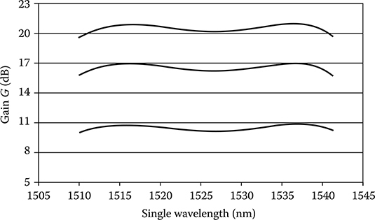
FIGURE 4.36 Gain of a Raman amplifier using a DCF and two pumps in positions designed to achieve the best possible uniformity within the fixed design gain and maximum pumps power constrains.
In the intermediate curve, the net average gain is 16.5 dB and the pump powers are 390 and 450 mW, while the gain flatness is 1.1 dB.
Finally, the lower curve exhibits an average gain of 10.5 dB with a flatness of 0.7 dB using two pumps with a power of 340 and 300 mW.
Globally, it is clear that there is a sort of trade-off between the flatness and the gain, due to the fact that in the adopted approximation, the local gain due to a pump is proportional to the pump power.
It has to be noted also that the coupling loss between the pumps and the active fiber is a key in determining the Raman gain.
Considering very wide band amplifiers, a flat gain over C + L band, a band of about 60 nm, can be achieved by three or four pumps and gain in excess of 21 dB has been reported in literature as shown in Figure 4.37 [71]. Advantages can also be achieved by the so-called double pass architecture, where the signal is reflected at one amplifier length to pass through the amplifying fiber two times in opposite directions [72]. This design, quite interesting since suitable for low levels of input signals, has been experimentally implemented observing a maximum gain of 22 dB gain with a noise figure smaller than 5 dB over all the C band [72].

FIGURE 4.37 Spectral gain of a Raman booster amplifier using a DCF and four pumps, whose power (always the same for each pump) is tuned to attain different values of the gain, and whose position was optimized to minimize gain ripple in a 60 nm band. (After Lewis, S.A.E. et al., Electron. Lett., 35(14), 1178, 1999.)

FIGURE 4.38 Gain of a lumped Raman amplifier designed to work in Wavelength (nm) the S band.
Finally, there is to consider another possible application of Raman amplifiers: amplification in the S band, where EDFAs cannot be used. Very good results have been achieved in this spectral area using high Raman efficiency fibers, as reported in [60] and shown in Figure 4.38 where a few experimental data reported in [60] are interpolated with the model presented in this section by adopting the parameters of a DCF and four pumps, whose power (always the same for each pump) is tuned up to a maximum of 330 mW, to attain different values of the gain and whose position was optimized to minimize gain ripple in the S band (from 1493 to 1523 nm).
Let us now consider the noise characterization of Raman amplifiers.
Starting from the ASE noise, we have to consider the noise equation and solve it to find the noise spectral density. Since the evolution of pumps and signal are known, it is not a difficult task and the following equation is obtained:
NA=ħω(G−12)+ħωαG L∫0dzG(z)(4.88)

(4.88)
The values of the ASE spectral density obtained with this equation are plotted in Figure 4.39 versus wavelength considering a single-pump-concentrated amplifier made by a DCF 30 km long whose parameters are reported in [68]. The results are compared with the simulated ASE spectral density reported in [68]. The simulation has been carried out using a model similar to that reported in Appendix D, taking into account a wide variety of phenomena.
The spectral density in the signal bandwidth is very well modeled by Equation 4.88 in a very large part of the spectrum. Near the pumps, the ASE spectral density is in reality much higher than that foreseen by Equation 4.88 due to the fact that parametric amplification caused by the pumps, which is not included in the simple model we are considering, amplifies ASE up to quite high powers.
As a consequence, even if the gain should be sufficient, no signal has to be within a guard bandwidth of about 50 nm from the pumps in order to avoid a high ASE zone.
If this rule is respected, Equation 4.88 model the ASE spectral density very well, and it can be used to evaluate the Raman amplifier noise factor obtaining

FIGURE 4.39 ASE noise spectrum for a single-pump Raman amplifier.
(After Bristiel, B. et al., IEEE Photonics Technol. Lett., 18(8), 980, 2006.)
NF=1+G(L)−1G(L)+2α L∫0dzG(z)(4.89)
(4.89)
A more accurate analytical solution of the noise equations can also be found taking into account time fluctuations (thus removing the stationary assumptions). In this way, a more accurate representation of the ASE noise can be achieved that is also valid for very high-gain amplifiers [68], where Equation 4.88 is less accurate. An example of noise figure calculation versus gain is reported in Figure 4.40 for an amplifier whose parameters are reported in [68] where it is also shown that similar curves agree very well with experimental results.
Among the noise term that we have neglected in simplifying the Raman equations, the RIN transfer from the pump to the signal is the most important; thus, a model for this noise source is useful when dealing with the design of systems including Raman amplifiers.
In order to study this phenomenon, following [68], it is needed to add to the system (4.84) the equations for the signal and the pumps RIN. These equations can be obtained from the complete model presented in Appendix D by applying to the complete RIN evolution equations the approximations already applied to the pumps and signal propagation equations.
The RIN equations can be solved analytically too, due to the knowledge of the signal and pumps evolution, so that the signal RIN at the output of the amplifier is given by Equation 4.90 is in good agreement with experience, as shown in [68], but for the case in which the noise in the bandwidth near the pump is considered.
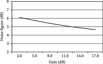
FIGURE 4.40 Raman amplifier noise factor versus net gain for an amplifier using 3 km of DCF fiber. (After Bristiel, B. et al., IEEE Photonics Technol. Lett., 18(8), 980, 2006.)
RINs,out=RINs,in+log(GR)[RINp,in+ħωp2P(0)αp(L−Le)](4.90)
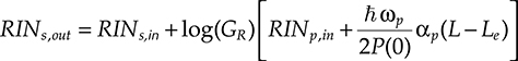
(4.90)
A last observation that can be important in the Raman lumped amplifiers design is that the effect of temperature can be important in degrading the amplifier noise performances. Just to make an example, an increase of the noise spectrum as great as 5 dB has been measured passing from 77 to 300 K at 1460 nm in a 9 km single-stage amplifier pumped by a pump of 850 mW at 1455 nm. In the same conditions, the peak gain at 1545 nm increases from 12 to 18 dB.
All the multistage techniques that are well established in the EDFA design can be adopted to design effective Raman amplifiers.
For example, multistage amplifiers can be devices with low-gain stages putting in between isolators that prevent the accumulation of double Rayleigh scattering and allows forward and backward pumps to be effectively separated.
Today Raman amplifiers are not considered as possible substitutes of EDFAs, even if this would be not impossible at least in high-performance systems, but are adopted as complementary amplification besides EDFAs. An exception of course is the case in which transmission in S band is needed, a case in which Raman amplifiers are the only solution.
4.3.4 Hybrid Raman-EDFA Amplifiers
Erbium-doped and Raman amplifiers can be usefully combined in very high-performance transmission systems. In this case, distributed Raman amplification can be used either to extend the bandwidth of EDFA amplifiers or to partially compensate the span loss via distributed amplification [60,73].
In the first case, the amplifier scheme is that shown in Figure 4.41. The optical signal is divided into bandwidth, C and L bands are amplified via specialized EDFAs, while the other bandwidths are amplified through concentrated Raman amplifiers.
This is a promising solution for ultra-high-capacity systems, even if balancing problems among amplifiers in the different bands can be difficult to solve.
The other application, however, is more than promising, and ultra-long-haul systems using this solution are already on the market.
The scheme of the hybrid amplifier is reported in Figure 4.42, while in Figure 4.43 the power profile along a link adopting hybrid amplifiers is compared with the power profile along a link adopting only concentrated EDFA amplifiers.
From Figure 4.42, some key advantages of using hybrid amplifiers can be seen immediately. From the fact that the Raman amplifier works as a low-noise preamplifier (it is distributed; thus, the noise figure is small) and from the general theory of cascaded amplifier, it is immediately deduced that the hybrid amplifier shall have a better noise figure with respect to an equivalent concentrated amplifier.
Thus, either a lower signal powers can be used or a higher loss can be tolerated. Alternatively, a longer transmission distance can be used between regenerators. This property explains why hybrid amplifiers are mostly used in ultra-long-haul systems, where the reach is key in the system value proposition.
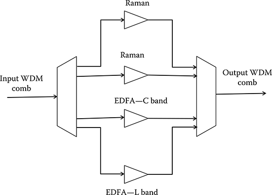
FIGURE 4.41 Block scheme of a wide band amplifier using EDFAs for C and L bands and Raman for S band.

FIGURE 4.42 One of the possible schemes of hybrid EDFA and Raman amplifier.
A second advantage is a more uniform gain along the length of the fiber. This gives rise to better signal to noise ratio performance and reduced nonlinear penalty.
Finally, the gain equalization, gain level correction, Add–Drop multiplexers, and dispersion compensation can all be placed in between the two stages of the EDFA, thus requiring no modification to the standard architecture and design of such subsystems.
On the other hand, there are also challenges in using hybrid amplifiers. A first challenge is constituted by the high Raman pump powers propagating in the transmission fiber. Pumps on the order of 500 mW or even 1 W are common for Raman-distributed amplifiers if using an SSMF transmission fiber. At these power levels, connectors are highly vulnerable to damage. In addition, there are issues associated with higher sensitivity to spurious reflections and to environmental and mechanical changes.
Careful optimization and engineering are needed to design practical hybrid amplifiers; however, despite all these difficulties, many ultra-long-haul systems adopt them.
The potential performances of hybrid amplifiers are illustrated in Figure 4.44 where SN0 and NF are shown for a high-performance hybrid amplifier [74]. Here SN0 is the signal to noise ratio at the amplifier output if the input signal is in a coherent state. It is not difficult to compare these figures with an equivalent two stages EDFA amplifier and recognize the advantage of the hybrid solution in having a small overall noise factor.

FIGURE 4.43 Signal power distribution along a line with EDFAs and with hybrid amplifiers.

FIGURE 4.44 Spectral distribution of SN0 and NF of a high-performance hybrid amplifier.
(After Optiwave White Papers. Hybrid amplifiers [Online], 2009, http://www.optiwave.com/literature/article_whitepaper.html (Accessed: May 15, 2010).)
4.4 Optical Filters
The concept of filter in optics is almost the same as that in electronics: a passive and linear system used generally to admit into a system only the signals in a determined bandwidth.
There are a great number of optical filters used for a wide variety of applications [16]. Here we will briefly review the most important filters used in telecommunication equipment.
Optical filter can be classified in two classes: periodic and nonperiodic filters.
In some filters, the transfer function, or the shape of the filter passband, repeats itself after a certain period. The period of such devices is called free spectral range (FSR).
The FSR usually depends on various physical parameters in the device, such as cavity or waveguide lengths.
The finesse of a periodic filter is a measure of the width of the transfer function. It is the ratio of FSR to the filter 3 dB bandwidth.
For all optical filters that are placed on the signal path, the attenuation is a fundamental characteristic, besides dispersion and passband shape.
4.4.1 Fixed Wavelength Optical Filters
4.4.1.1 Grating Filters
One implementation of a fixed filter is the diffraction grating [16]. A bulk diffraction grating is essentially a flat layer of transparent material (e.g., glass or plastic) with a row of parallel grooves cut into it. The grating separates light into its wavelengths component by reflecting light incident with the grooves. The reflected spectral components interfere at the grating output and, at certain angles, only one wavelength interferes constructively; all others cancel by destructive interference.
This allows the desired wavelength to be selected by placing a spatial filter (essentially a hole) filter at the proper angle.
A grating can be also impressed onto a guiding structure, like a fiber or a monolithic waveguide. These gratings can be either transmissive or reflective.
4.4.1.2 Fiber Bragg Gratings
A fiber Bragg grating is a periodic or pseudo-periodic perturbation of the effective refractive index in the core of an optical fiber [16]. Typically, the perturbation is approximately periodic over a certain length from a few millimeters to centimeters for long gratings, and the period is on the order of hundreds of nanometers, or much longer for long-period fiber gratings.
The refractive index perturbation leads to the reflection of light in a narrow range of wavelengths, for which a Bragg condition is satisfied
2π∧=22πλneff(4.91)
![]()
(4.91)
where
Λ is the grating period
λ is the vacuum wavelength
neff is the effective refractive index of light in the fiber
Essentially, the condition means that the wave number of the grating matches the difference of the (opposite) wave vectors of the incident and reflected waves.
In that case, the complex amplitudes corresponding to reflected field contributions from different parts of the grating are all in phase so that they can add up constructively. Even a weak modulation index (with an amplitude of, e.g., 10−4) is sufficient for achieving nearly total reflection, if the grating is sufficiently long (e.g., a few millimeters).
Light at other wavelengths, not satisfying the Bragg condition, is nearly not affected by the Bragg grating, except for some side lobes that frequently occur in the reflection spectrum (but can be suppressed by apodization of the grating [47]).
The reflection bandwidth of a fiber grating, which is typically well below 1 nm, depends on both the length and the strength of the refractive index modulation. The narrowest bandwidth values are obtained for long gratings with weak index modulation. Large bandwidths may be achieved not only with short and strong gratings, but also with aperiodic designs.
4.4.1.3 Thin-Film Interference Filters
Thin-film filters offer another approach for fixed optical filtering [16]. These filters are similar to fiber Bragg grating devices with the exception that they are fabricated by depositing alternating layers of low-index and high-index materials onto a substrate layer. Thin-film filter technology allows the shape of the filter to be designed on the system needs since almost every pass-band shape can be realized via deposition of a sufficiently high number of layers. The main limitation is on the filter bandwidth that cannot be too tight. Typical values of the thin-film filter bandwidth are 1 nm at a wavelength of 1.5 μm.
4.4.2 Tunable Optical Filters
4.4.2.1 Etalon
The etalon [16], or Fabry–Perot filter, consists of a single cavity formed by two parallel mirrors. Light from an input fiber enters the cavity and reflects a number of times between the mirrors. By adjusting the distance between the mirrors, the cavity resonates on the desired wavelength that passes through the cavity, while the other wavelengths are reflected.
The varying transmission function of an etalon is caused by interference between the multiple reflections of light between the two reflecting surfaces. Constructive interference occurs if the transmitted beams are in phase, and this corresponds to a high-transmission peak of the etalon. If the transmitted beams are out-of-phase, destructive interference occurs and this corresponds to a transmission minimum. Whether the multiply-reflected beams are in-phase or not depends on the wavelength (λ) of the light (in vacuum), the angle the light travels through the etalon (θ), the thickness of the etalon (ℓ), and the refractive index of the material between the reflecting surfaces (n).
The phase difference between each succeeding reflection is given by δ:
δ=(2πλ)2nlcosθ=(2ωc)nlcosθ(4.92)
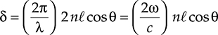
(4.92)
If both surfaces have a reflectance R, the transmittance function of the etalon is given by the following:
H(ω)=(1−R)21−R2−2Rcos[(2ω/c)nlcosθ]=11+Fsin2[δ(ω)](4.93)
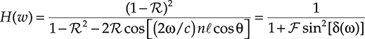
(4.93)
where F= R /(1 − R)2 is the coefficient of finesse.

FIGURE 4.45 Periodic transmission of an etalon for different values of the finesse.
The transmission of an etalon as a function of wavelength is plotted in Figure 4.45 for different values of the finesse coefficient. A high-finesse etalon shows sharper peaks and lower transmission minima than a low-finesse etalon.
The etalon is probably the most used optical filter and many types of etalons exist for different applications.
Air-spaced etalons have fused silica substrates and an air gap between the cavity mirrors; the outside-facets are antireflection coatings to prevent extraneous interference patterns from forming. Spacers determine the parallelism of the mirrors and the etalon’s FSR.
Solid state etalons typically have fused silica substrates and a solid material, transparent at the desired wavelengths, to form the etalon body. Dielectric (or, rarely, metallic) coatings provide the reflectivity necessary for the required finesse. The faces are ground, polished, and figured typically to better than 1/100 flatness to achieve the desired control of the transfer function. Solid state etalons cannot be tuned by moving the mirrors, but tuning can be achieved with other means, for example, changing the material refraction index.
Both air spaced and solid etalons exist in miniaturized versions for telecommunication applications.
To overcome the limit of the thinness of a solid etalon and yet retain its mechanical strength, Deposited etalons exist, realized by means of layers deposited on a substrate.
4.4.2.2 Mach Zehnder Interferometer
In an integrated Mach Zehnder interferometer (MZI) [16], a splitter splits the incoming wave into two waveguides and a combiner recombines the signals at the outputs of the waveguides as shown in Figure 4.46. In the figure, an example of filter working is also indicated, in particular the response to two signals entering from the same port.
An adjustable delay element controls the optical path length in one of the waveguides, resulting in a phase difference between the two signals when they are recombined. In order to widen the bandpass, sometimes the MZI branches are not straight, as also shown in the figure.
Wavelengths for which the phase difference is 180 are filtered out. By constructing a chain of these elements, a single desired optical wavelength can be selected [75].
While the MZI chain promises to be a low-cost device because it can be fabricated on semiconductor material [76], its tuning control is complex, requiring a delay element setting in each stage to be dependent on the settings in previous stages of the chain.

FIGURE 4.46 Block scheme of a wide band MZI filter.
4.4.2.3 Microrings Filters
Optical microring resonators (OMRs) are versatile elements for implementing filtering function in integrated photonic circuits [77].
A microring is generally constituted by a ring waveguide resonator with two tangent waveguides that, in the nearer point, passes at a very small distance from the ring. This distance, which is a critical parameter determining the coupling efficiency between the resonator and the input/output waveguides, is called characteristic gap.
Each ring, with its input and output ports, constitutes a single-pole add/drop periodic filter: resonant frequencies are sent from the input to the so-called drop port, while nonresonant frequencies are sent to the so-called line port. This behavior is represented in Figure 4.47.
The single-pole filter has a Lorentzian bandpass characteristic and can be used as building blocks for multipole add–drop filters (see Figure 4.47). The bandwidth of the single-pole filter is given by [78]
Δω=ω0Σ2j=01/Qj(4.94)
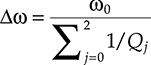
(4.94)
where
ω0 is the resonant angular frequency
Q0 is the circular cavity quality factor
Q1 and Q2 are the quality factors of the coupling between the input and the output guides, respectively, and are given by
Qj=πω0ρnecκ(4.95)
![]()
(4.95)
where
ρ is the ring radius
ne is the effective mode index
c is the light speed in vacuum
κ is the coupling coefficient

FIGURE 4.47 Scheme of a three-pole multiring filter.

FIGURE 4.48 Notch and passband filtering characteristic of a two poles multiring filter: theoretical (dotted line) and measured (continuous line) characteristics.
(After Romagnoli, M. et al., Proc. SPIE, 6996, 699611, 2008.)
As shown in Figure 4.47, microrings can be coupled together to build a complex filter with sharp transfer functions. In Figure 4.48 [79], the transfer function measured for a two-stage microring filter is compared with its theoretical estimation.
The weakness of this technique, which has as many advantages in terms of power consumption, dimension, and functionality, is the loss that today are still too high for the use in the signal line. However, microrings are more and more diffused in the field in which losses are less critical.
4.4.3 WDM Multiplexers and Demultiplexers
In principle, several types of optical filters are suitable to form arrays working as multiplexers and demultiplexers.
For example, several CWDM multiplexers are realized as shown in Figure 4.49 with an array of thin-film filters.
The way in which the filters are arranged implies that the different channels undergo a different loss. This problem is generally overcome by arranging the filters in the demultiplexer in the inverse order with respect to the multiplexer arrangement. Thus, the channel undergoing the greater loss at the demultiplexer experiment the smaller at the multiplexer and so on.
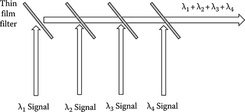
FIGURE 4.49 Example of WDM mux/demux realized with thin film filters.
Thin-film filters have also the quality of being low loss and very controlled in shape; thus, they constitute excellent elements for mux/demux.
Unfortunately, it is very difficult to obtain thin-film filters suitable for processing DWDM channels, whose distance is 100 or even 50 GHz with a modulation of 10 Gbit/s, while channels modulated at 40 Gbit/s are spaced 100 or 200 GHz.
To work at this small spacing, thin-film filters require a too high number of different coatings decreasing the repeatability and generating too great prices to be adopted in real products.
Practically all DWDM systems use array waveguide (AWG) multiplexers/demultiplexers. Figure 4.50 shows a schematic layout of an AWG demultiplexer; a multiplexer is identical but for the fact that several signals enter from the waveguides that are the demultiplexer output and the WDM comb emerges from the demultiplexer input. The device consists of three main parts which are as follows:
Multiple input and output waveguides
Two slab waveguide star couplers (also called free propagation region [FPR])
A dispersive waveguide array with the equal length difference between adjacent waveguides Dispersive array

FIGURE 4.50 Scheme of an AWG demultiplexer.
Table 4.12 Characteristics of a Realistic AWG Used for Multiplexing/Demultiplexing DWDM Channels

The operation principle of the AWG multiplexer/demultiplexer is described as follows. A DWDM signal launched into one of the input waveguides will be diffracted in the first slab region and coupled into the arrayed waveguide by the first FPR. The length of the AWGs has been designed such that the optical path length difference (ΔL) between adjacent AWGs equals an integer (m) multiple of the central wavelength (λc) of the demultiplexer.
As a consequence, the field distribution at the input aperture will be reproduced at the output aperture. Therefore, at this center wavelength, the light focuses on the center of the image plane (provided that the input waveguide is centered in the input plane). If the input wavelength is detuned from this central wavelength, phase changes occur in the array branches.
Due to the constant path length difference between adjacent waveguides, this phase change increases linearly from the inner to outer AWGs, which causes the wavefront to be tilted at the output aperture. Consequently, the focal point in the image plane is shifted away from the center. By placing receiver waveguides at proper positions along the image plane, spatial separation of the different wavelength channels is obtained.
AWG are able to process a great number of nearby channels with acceptable loss and a great reproducibility and their structure allows even bigger mux/demux to be designed by cascaded of suitably designed AWG.
The performance of a realistic AWG used for multiplexing/demultiplexing DWDM channels is reported in Table 4.12.
REFERENCES
1.. Snider, A. W., Love, J. D., Optical Waveguide Theory, Chapman & Hall, London, U.K., 1983, ISBN-13: 978-0412099502.
2.. Hunger, H. G., Planar Optical Waveguides and Fibers, Clarendon Press, Oxford, U.K., 1977.
3.. Gloge, D., Weakly guiding fibres, Applied Optics, 11(10), 2252–2258 (1971).
4.. He, Y., Shi, F., Beam Propagation Method and Microlens Design for Optical Coupling: Finite-Difference Full-Vectorial Beam Propagation Method Development and Microlens Design for Fiber to Laser Diode Coupling, VDM Verlag, Berlin, Dr. Müller, s.l., 2010, ISBN-13: 978-3639209723.
Skutnik, B.J., Moran, K.B., Spaniol, S., Optical fibers for improved low loss coupling of optical, Proceedings of Progress in Biomedical Optics and Imaging, San Jose, CA, January 27–28, s.l., 2004.
6.. Boyd, R. W., Nonlinear Optics, Academic Press, San Diego, CA, 2008, ISBN-13: 978-0123694706.
7.. Agrawal, G. P., Nonlinear Fiber Optics, 4th edn., Academic press, San Diego, CA, 2006, ISBN-13:978-0123695161.
8.. Pool, C. D., Wagner, R. E., Phenomenological approach to polarization dispersion in single mode fibers, Electronics Letters, 22, 1029–1030 (1986).
9.. Curti, F., Daino, B., Mao, Q., Matera, F., Someda, C. G., Concatenation of polarization dispersion in single mode fibers, Electronics Letters, 25, 290–292 (1989).
10.. Betti, S., Curt, F., Daino, B., De Marchis, G., Iannone, E., Matera, F., Evolution of the bandwidth of the principal states of polarization in single mode fibers, Optics Letters, 16, 467–469 (1991).
11.. De Angelis, G., Galtarossa, A., Gianello, G., Matera, F., Schiano, M., Time evolution of polarization mode dispersion in a long terrestrial link, IEEE Journal of Lightwave Technology, 10, 552–555 (1992).
12.. De Marchis, G., Iannone, E., Polarization dispersion in single mode optical fibers: A simpler formulation based on pulse envelope propagation, Microwave and Optical Technology Letters, 4, 75–77 (1991).
13.. Bononi, A., Vannucci, A., Statistics of the Jones matrix of fibers affected by polarization mode dispersion, Optics Letters, 26, 675–677 (2001).
14.. Curti, F., Daino, B., De Marchis, G., Matera, F., Statistical treatment of the evolution of the principal states of polarization in single mode fibers, IEEE Journal of Lightwave Technology, 8, 1162–1166 (1990).
15.. Gordon, J. P., Kogelnik, H., PMD fundamentals: Polarization mode dispersion in optical fibers, Proceedings of the National Academy of Sciences, 97, 4541–4550 (2000).
16.. Born, M., Wolf, E., Principles of Optics: Electromagnetic Theory of Propagation, Interference and Diffraction of Light, 7th edn., Cambridge University Press, Cambridge, U.K., s.l., 1999, ISBN-13: 978-0521642224.
17.. Shen, Y. R., The Principles of Nonlinear Optics, Wiley Interscience, Hoboken, NJ, s.l., 2002, ISBN-13: 978-0471430803.
18.. Iannone, E., Matera, F., Mecozzi, A., Settembre, M., Nonlinear Optical Communication Networks— Appendix A1, Wiley, New York, s.l., 1998, ISBN-13: 978-0471152705.
19.. Gordon, J. P., Mollenauer, L. F., Solitons in Optical Fibers: Fundamentals and Applications, 1st edn., Academic Press (Kindle Edition), Burlington, MA, s.l., 2006, ASIN: B000PY3CWE.
20.. Hamza, M. Y., Tariq, S., Split step Fourier method based pulse propagation model for nonlinear fiber optics, International Conference on Electrical Engineering ICEE ʻ07, Hong Kong, IEEE, s.l., pp. 1–5, July 8–12, 2007.
21. Chraplyvy, A. R., Limitations on lightwave communications imposed by optical fiber nonlinearities, Journal of Lightwave Technology, 8, 1548–1557 (1990).
22.. Kivshar, S. Y., Agrawal, G., Optical Solitons: From Fibers to Photonic Crystals, Academic Press, San Diego, CA, s.l., 2003, ISBN-13: 978-0124105904.
23.. Tkach, R. W., Chraplyvy, A. R., Forghieri, F., Gnauck, A. H., Derosier, R. M., Four photon mixing and high speed WDM systems, IEEE Journal of Lightwave Technology, 13, 841–849 (1995).
24.. Shibate, N., Horigudhi, M., Edahiro, T., Raman spectra of binary high-silica glasses and fibers containing GeO2, P2O5 and B2O3, Journal of Non-Crystalline Solids, 45, 115–126 (1981).
25.. Cotter, D., Observation of stimulated Brillouin scattering in low loss silica fiber at 1.3 μm, Electronics Letters, 18, 495–496 (1982).
26.. Buckland, E. L., Boyd, R. W., Electrostrictive contribution to the intensity-dependent refractive index of optical fiber, Optics Letters, 21, 1117–1119 (1996).
27.. Nikles, M., Thevenaz, L., Robert, P. A., Brillouin gain spectrum characterization in single-mode optical fiber, IEEE Journal of Lightwave Technology, 15, 1842–1851 (1997).
28.. Mendez, A., Morse, T. F., Specialty Optical Fibers Handbook, Academic Press, Burlington, MA, s.l., 2007, ISBN-13: 978-0123694065.
Li, M. J., Chen, X., Nolan, D. A., Berkey, G. E., Wang, J., Wood, W. A., Zenteno, L. A., High bandwidth single polarization fiber with elliptical central air hole, Proceedings of the 20th Annual Meeting of the Lasers and Electro-Optics Society, Lake Buena Vista, FL, IEEE, pp. 3454–3460, December 19, 2007.
30.. Ramachandran, S., Fiber Based Dispersion Compensation, Springer, New York, s.l., 2007, ISBN-13: 978-0387403472.
31.. Wandel, M., Kristensen, P., Veng, T., Qian, Y., Le, Q., Gruner-Nielsen, L., Dispersion compensating fibers for non-zero dispersion fibers, Optical Fiber Communication Conference and Exhibit, OFC 2002, Anaheim, CA, IEEE, s.l., May 17–22, 2002.
32. Richardson, D. J., Belardi, W., Furusawa, K., Price, J. H. V., Malinowski, A., Monro, T. M., Holey fibers: Fundamentals and applications. Summaries of papers presented at the Lasers and Electro-Optics, CLEO ʻ02, Long Beach, CA, IEEE, s.l., Vol. 1, pp. 453–454, 2002.
33.. Poli, F., Cucinotta, A., Selleri, S., Photonic Crystal Fibers: Properties and Applications, Springer, New York, s.l., 2009, ISBN-13: 978-9048176090.
34.. Borzycki, K., Holey fibers-application issues, Proceedings of the 3rd International Conference on Transparent Optical Networks, Cracow, Poland, s.n., pp. 92–95, June 18–21, 2001.
35.. Bjarklev, A., Riishede, J., Photonic crystal fibers—A variety of applications, Proceedings of the 4th International Conference on Transparent Optical Networks, Warsaw, Poland, Vol. 2, p. 97, April 21–25, 2002.
36. Ming-Yang, C., Polarization-maintaining large-mode-area microstructured-core optical fibers, IEEE Journal of Lightwave Technology, 26, 13 (2008).
37.. Hayes, J. et al., Advanced fibre designs for high power laser beam delivery and generation, High Power Diode Lasers and Systems Conference, Coventry, U.K., s.n., pp. 1–2, October 14–15, 2009.
38.. Akowuah, E. K. et al., An endlessly single-mode photonic crystal fiber with low chromatic dispersion, and bend and rotational insensitivity, IEEE Journal of Lightwave Technology, 27(17), 3940–3947 (2009).
39.. Ortigosa-Blanch, A. et al., Highly birefringent photonic crystal fibres, Optics Letters, 25(18), 1325–1327 (2000).
40. Nolan, D. A. et al., Single-polarization fiber with a high extinction ratio, Optics Letters, 29(16), 1855 (2004).
41. Zenteno, L. A. et al., Suppression of Raman gain in single-transverse-mode dual-hole-assisted fiber, Optics Express, 13(22), 8921–8926 (2005).
42.. Hogari, K., Yamada, Y., Toge, K., Novel optical fiber cables with ultrahigh density, Journal of Lightwave Technology, 26(17), 3104–3109 (2008).
43.. Hearle, J. W. S., High-Performance Fibres, Woodhead Publishing Ltd., Cambridge, England, s.l., 2001, ISBN: 1855735393.
44.. Loudon, R., The Quantum Theory of Light, 3rd edn., Oxford Science Publications, Oxford, NY, s.l., 2000, June 2001. ISBN: 0198501765.
45.. Itzykson, C., Zuber, J.-B., Quantum Field Theory, New Edition, Dover Publications, New York, s.l., 2000, ISBN: 0486445682.
46. Holden, H., Øksendal, B., Ubøe, J., Zhang, T., Stochastic Partial Differential Equations: A Modeling, White Noise Functional Approach, Springer, New York, s.l., 2009, ISBN-13: 978-0387894874.
47.. Ramaswami, R., Sivarajan, K. R., Sasaki, G., Optical Networks: A Practical Perspective, 3rd edn., Morgan Kaufmann, San Francisco, CA, s.l., 2009, ISBN-13: 978-0123740922.
48.. Desurvire, E., Erbium-Doped Fiber Amplifiers: Principles and Applications, Wiley, New York, s.l., 1994, ISBN-13: 978-0471589778.
49.. Malin Premarante and Govind P. Agrawal Light Propagation in Gain Media: Optical Amplifiers, Cambridge University Press (March 14, 2011), Cambridge, ISBN-13:978–0521493482.
50.. Wyart, J. F., Blaise, J., Bidelman, W. P., Cowley, C. R., Energy levels and transition probabilities in doubly-ionized erbium (Er 111), Physica Scripta, 56, 446–458 (1997).
Tanabe, S., Development of rare-earth doped fiber amplifiers for broad band wavelength-division-multiplexing telecommunication. In Photonics Based on Wavelength Integration and Manipulation, The Institute of Pure and Applied Physics—IPAP Books, Tokyo, Japan, s.l., pp. 101–112, 2005.
52. Ohishi, Y., Yamada, M., Kanamori, T., Sudo, S., Shimizu, M., Low-noise operation of fluoridebased erbium-doped fiber amplifiers with 4I11/2-level pumping, Optics Letters, 22(16), 1235–1237 (1997).
53.. Girarda, S., Marcandella, C., Origlio, G., Ouerdane, Y., Boukenter, A., Meunier, J.-P., Radiationinduced defects in fluorine-doped silica-based optical fibers: Influence of a pre-loading with H2, Journal of Non-Crystalline Solids, 335(18–21), 1089–1091 (2009).
54.. Pedersen, B., Bjarklev, A., Povlsen, J. H., Design of erbium doped fibre amplifiers for 980 nm or 1480 nm pumping, Electronics Letters, 27(3), 255–257 (1991).
55.. Thyagarajan, K., Anand, J. K., Intrinsically gain-flattened staircase profile erbium doped fiber amplifier, Optics Communications, 222(1–6), 227–233 (2003).
56.. Bae, J. K., Bae, J., Kim, S. H., Park, N., Lee, S. B., Dynamic EDFA gain-flattening filter using two LPFGs with divided coil heaters, IEEE Photonics Technology Letters, 17(6), 1226–1228 (2005).
57.. Yu, A., O’Mahony, M. J. Analysis of dual-stage erbium-doped fibre amplifiers with passive equalisation filters, IEE Proceedings on Optoelectronics, 146(3), 153–158 (1999).
58.. Headley, C., Agrawal, G. (Eds.), Raman Amplification in Fiber Optical Communication Systems, Prentice Hall Academic Press, Burlington, MA, s.l., 2004, ISBN-13: 978-0120445066.
59.. He, J., Guo, T., Gu, W., Xu, D., Study on optimal design broadband and flat-gain multi-wavelength pumped fiber Raman amplifiers, Journal of Optical Communications, 24, online 42, 1–4 (2003).
60.. Islam, M. N. Raman amplifiers for telecommunications, IEEE Journal of Selected Topics in Quantum Electronics, 8(3), 548–558 (2002).
61.. Tang, M. Gong, Y. D., Shum, P., Design of double-pass dispersion-compensated Raman amplifiers for improved efficiency: Guidelines and optimizations, IEEE Journal of Lightwave Technology, 22(8), 1899–1908 (2004).
62.. Hansen, P. B., Jacobovitz-Veselka, G., Gruner-Nielsen, L., Stentz, A. J., Raman amplification for loss compensation in dispersion compensating fibre modules, Electronics Letters, 34(11), 1136–1137 (1998).
63.. Dung, J.-C., Sien, C., Characteristic of the reflective type Raman amplification in a dispersion compensating fiber, Proceedings of the 5th Pacific Rim Conference on Lasers and Electro-Optics, Taipei, Taiwan, Vol. 1, p. 4, December 2003.
64.. Matsuda, T., Kotanigawa, T., Naka, A., Imai, T., 62×42.7 Gbit/s (2.5 Tbit/s) WDM signal transmission over 2200 km with broadband distributed Raman amplification, Electronics Letters, 38(15), 818–819 (2002).
65.. Banoni, M., Fuochi, A., Transient gain dynamics in saturated Raman amplifiers with multiple counter-propagating pumps, Optical Fiber Conference, OFC, Atlanta, GA, IEEE, Vol. 1, p. 439, March 23–28, 2003.
66.. Islam, M. N., Alam, M. S., Design of multiple pumps Raman amplifiers for optical communication systems, Journal of Optical Communications, 27(2), 75–78 (2006).
67.. Pustovskikh, S. M., Kobtsev, A. A., Improvement of Raman amplifier gain flatness by broadband pumping sources, Laser Physics, 14(12), 1488–1491 (2004).
68.. Bristiel, B., Jiang, S., Gallion, P., Pincemin, E., New model of noise figure and RIN transfer in fiber Raman amplifiers, IEEE Photonics Technology Letters, 18(8), 980–982 (2006).
69.. Fludger, C., Handerek, V., Jolley, N., Mears, R. J., Fundamental noise limits in broadband Raman amplifiers, Optical Fiber Communication Conference, OSA, Anaheim, CA, March 17, 2001.
70.. Namiki, S., Recent advances in Raman amplifiers, European Conference on Optical Communications (ECOC), Amsterdam, the Netherlands, Vol. Tutorial, October 1–4, 2001.
71.. Lewis, S. A. E., Chernikov, S. V., Taylor, J. R., Gain and saturation characteristics of dual wavelength-pumped silica-fibre Raman amplifier, Electronics Letters, 35(14), 1178–1179 (1999).
Tang, M., Gong, Y. D., Shum, P., Dynamic properties of double-pass discrete Raman amplifier with FBG-based all-optical gain clamping technique, IEEE Photonics Technology Letters, 16(3), 768–770 (2004).
73.. Carena, A., Curri, V., Poggiolini, P., On the optimization of hybrid Raman/Erbium-doped fiber amplifiers, IEEE Photonics Technology Letters, 13(11), 1170–1172 (2001).
74.. Optiwave White Papers. Hybrid amplifiers [Online], 2009, http://www.optiwave.com/literature/article_whitepaper.html (Riportato: May 15, 2010).
75.. Kuznetsov, M., Cascaded coupler Mach-Zehnder channel dropping filters for wavelength-divi-sion-multiplexed optical systems, IEEE Journal of Lightwave Technology, 12(2), 226–230 (1994).
76.. Okayama, H., Yaegashi, H., Ogawa, Y., Sub-micron Si waveguide design for polarization independent Mach-Zehnder filter, Proceedings of the 6th International Conference on Group IV Photonics, GFP ʻ09, San Francisco, CA, IEEE, Vol. 1, September 9–11, 2009.
77.. Popovic, M. A., Barwicz, T., Watts, M., Rakich, P. T., Dahlem, M. S., Gan, F., Holzwarth, C. W., Socci, L., Smith, H. I., Ippen, E. P., Kartner, F. X., Strong-confinement microring resonator photonic circuits, Proceedings of the 20th Annual Meeting of the Lasers and Electro-Optics Society, Lake Buena Vista, FL, IEEE, pp. 399–400, October 21–25, 2007.
78.. Hossein-Zadeh, M., Vahala, K. J., Importance of intrinsic-Q in microring-based optical filters and dispersion-compensation devices, IEEE Photonics Technology Letters, 19(14), 1045–1047 (2007).
79.. Romagnoli, M., Socci, L., Bolla, L., Ghidini, S., Galli, P., Rampinini, C., Mutinati, G., Nottola, A., Cabas, A., Doneda, S., Di Muri, M., Morson, R., Tomasi, T., Zuliani, G., Lorenzotti, S., Chacon, D., Marinoni, S., Corsini, R., Giacometti, F., Sardo, S., Gentili, M., Grasso, G., Silicon photonics in Pirelli, Proceedings of SPIE, 6996, 699611-699611-8 (2008), doi:10.1117/12.786539.