
9 Next Generation Transmission Systems Enabling Technologies, Architectures, and Performances
9.1 Introduction
In Chapter 6 we have discussed Dense Wavelength Division Multiplexing (DWDM) technologies for implementing high capacity very long reach optical transmission systems.
In that chapter, it has been shown as transmission systems with an overall capacity in excess of 2 Tbit/s and a reach longer than 2000 km can be designed using direct detection and in-line optical amplification.
From the point of view of the product capacity-reach it seems that these figures are sufficient to satisfy the needs of telecom carriers for the time being.
As a matter of fact, the need of a new generation of transmission systems does not emerge from the need of increasing the transmission capacity or the system reach, but comes from other reasons.
The fast increase of the traffic in American and European networks is due neither to the increase of the network nodes, whose number remains almost constant, nor to the increase of the network subscribers, that is very slow. What is driving the traffic increase is the increase in the bandwidth required by each subscriber.
This means that the traffic pattern remains statistically constant, while the service bundle offered by carriers differentiates, requiring to the transport layer to increase more and more the number of wavelengths routed along the same network routes.
If the number of wavelengths along a network route is huge, they are demultiplexed and multiplexed uselessly several times, since they should not to be separated. Moreover, every time they traverse a wavelength switch, several management controls have to be done to monitor the correct routing of every wavelength, even if they are directed toward the same direction. Last, but not least, the switching error probability increases with increasing the number of wavelengths.
The request to bundle together in the same network entity (a high capacity transport connection) a great amount of traffic directed toward the same end node is thus natural, and the most direct way to do that is to adopt a higher bit rate. The introduction of 40 Gbit/s in the network was done to alleviate this problem, but it is not enough. Thus a higher speed of the order of 100 Gbit/s is required.
Besides network design needs, hardware design requirements also call for a bit rate much higher than 10 Gbit/s.
Even if the increasing quality of transceivers generated signals will probably bring to a reduction of transponders footprint, the DWDM systems real estate is in any case huge. A 200-channel system using 10 Gbit/s transmission and C + L band amplification needs 100 working and 100 protection transponders even if XFPs are used to compact two channels per transponder.
On a standard Advanced Telecommunications Computing Architecture (ATCA) platform, this means 13 subracks and thus 5 racks only for transponders. This is a huge real estate, greater that that needed for a 30 Tbit/s router.
The only way that seems possible to achieve a strong footprint reduction is to increase greatly the bit rate. For example, assuming that a 100 Gbit/s transponder will occupy a two rack-units card (four times the footprint assumed for 10 Gbit/s), a system with a capacity of 2 Tbit/s using 100 Gbit/s channels will occupy 80 rack units for transponders, that is 5 ATCA subracks, much less than 13 needed in the 10 Gbit/s case.
Moreover, if the power consumption per unit capacity will continue to decrease with increasing the bit rate as that occurred when moving from 2.5 to 10 Gbit/s and from 10 to 40 Gbit/s, a strong decrease of power consumption is also probable if the bit rate is increased up to 100 Gbit/s.
Finally, the convergence on IP networking renders requirements related to routers architecture very important. As detailed in Chapter 7, in order to fully exploit the advances in electronics, routers line cards need to increase the speed of the memories implementing the input queues and of the associated processors.
Also this trend calls for a line bit-rate increase so that useless multiplexing and demultiplexing stages in the line cards need not be forcefully implemented.
If all the above reasons push the evolution of transmission systems toward an increase of the bit-rate, designing systems at 100 Gbit/s is a formidable challenge.
As a matter of fact, the presence of a great number of deployed transmission lines designed for 10 and 40 Gbit/s imposes a set of quite stringent requirements to practical 100 Gbit/s transmission systems.
In particular, 100 Gbit/s channels should be transmitted for distances of the order of magnitude of 1000 km on existing lines and should coexist with 10 and 40 Gbit/s channels without requiring disruption of present services.
Meeting these requirements is surely not possible with the same transmission technologies adopted at lower rates, due to the way in which various transmission impairments affects their performances; thus a complete redesign of transmission systems is needed.
In this chapter we will analyze the various alternatives for 100 Gbit/s transmission, taking into account different applications in the telecommunication network.
9.2 100 Gbit/s Transmission Issues
The first step to do in order to approach the problem of 100 Gbit/s long haul transmission is to understand impairments thwarting conventional transmission at a such a high speed to individuate potential solutions.
In general, solutions to transmission impairments can be attained either via the use of suitable devices to eliminate or compensate the impairing effect or shaping the transmission format and the detection strategy to be less sensible to the considered effect.
We will consider compensation technique in this section while advanced modulation formats and detection techniques will be reviewed in the next two sections.
9.2.1 Optical Signal to Noise Ratio Reduction
The first effect of the bit rate increase is the SNo reduction due to the increase of the required optical filter bandwidth.
The SNo is inversely proportional to the optical bandwidth, thus it can seem that the impact of increasing the bit-rate by a factor 10 with respect to 10 Gbit/s reflects in the need of an SN0 10 dB greater.
Even if this is a good first approximation, two effects could reduce the needed SN0 increase. First, the signal statistical distribution is not Gaussian. Second, and potentially more important, while in practice it is very difficult in a 10 Gbit/s system to maintain the optical bandwidth equal to the bit rate, it is much easier at 100 Gbit/s. Thus the extra optical noise power is greater at 10 Gbit/s.
In order to verify the impact of the bit-rate increase on the needed SNo, let us use the correct error probability model introduced for amplified systems in Chapter 6.
Assuming that no pattern effect is present and that thermal noise at the receiver is negligible with respect to the Amplified Spontaneous Emission (ASE) noise, the error probability expression (6.65) relative to an intensity modulated system with in-line amplifiers simplifies as
BER=12e−(γSNo−2Moe)(2Moe/γSNo)2Moe+12e−SNoMoe[X(SNo)/(1+X(SNo))−γX(SNo)/Moe][1+X(SNo)]2Moe(9.1a)
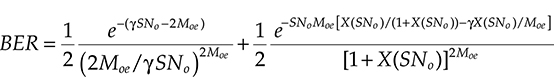
X(SNo)=−γSNo+Moe+√Moe√(γSNo+Moe)(9.1b)
![]()
(compare Equations 6.65a and b)
where
Cth = γSNo /Moe is the threshold value in terms of a fraction of the signal to noise ratio at the optical level
Moe is the ratio between the unilateral optical bandwidth and the electrical bandwidth (often approximated with the bit rate R)
Moreover, the saddle point approximation has been further simplified assuming SNo >> Moe.
Naturally, for each value of SNo the decision threshold (thus γ) has to be optimized.
To reflect the practical difficulty in implementing stable optical filters with a very small bandwidth, we will assume that at 10 Gbit/s, a filter with 60 GHz bandwidth (Moe = 6) is used, corresponding in wavelength to a bandwidth of about 0.5 nm at 1.55 μm. The filter bandwidth is increased at 120 GHz (1 nm) for the 40 (Moe = 3) and to 200 GHz at 100 Gbit/s (Moe = 2).
Passing from Moe = 6 to Moe = 3 to Moe = 2 implies that the SNo corresponding to a bit error rate (BER) of 10−12 passes from 15.4 to 18.3 to 20 dB.
This is a correction not completely insignificant to the value ΔSNo = 10 dB that was estimated at first glance if a fixed error probability has to be maintained passing from 10 to 100 Gbit/s.
Naturally, this does not mean that the performances get better by increasing Moe.
As a matter of fact, if we take into account the increase of the ASE bandwidth related to the increase of Moe, we discover that the power needed to achieve an error probability of 10−12 slightly increases by 6% passing from Moe = 2 to Moe = 3 and increases again by another 3% passing to Moe = 6.
In any case, considering the SNo, any change in Moe has to be considered.
In Chapter 6, we have seen that in an optically amplified line, the ASE spectral density is proportional to the number of spans, thus to the link length.
Let us imagine having a link 2500 km long designed for 10 Gbit/s, constituted by 50 spans of 50 km each. If the Optical Signal to Noise ratio has to increase by 10 dB passing to 100 Gbit/s, this means that, once the transmitted power is fixed, whose value is determined by the nonlinear effects, the link has to be shortened by a factor 10. In other words, the combination of nonlinear effects limiting the transmitted power and the increase of ASE noise causes a signal at 100 Gbit/s to propagate for a distance 10 times smaller with respect to a signal at 10 Gbit/s.
Besides improving the amplifiers design to reduce the noise factor, there is no other way of compensating the ASE effect. On the other hand, we know from Chapter 4, that optical amplifiers are quite near the ideal quantum performances, thus there is no great improvement to attain from amplifiers design, at least as far as quantum coherent states are propagated into the fiber.
It is possible to design parametric amplifiers, where the ASE noise spectral density is not uniform along the different polarizations. If a parametric amplifier is used to reduce the ASE along a polarization at the expense of that along the orthogonal one, the signal could be transmitted along the low ASE polarization thus improving the SNo.
Unfortunately, the resulting quantum state of the optical field at the output of such an amplifier is not a coherent state and such nonclassical field states tend to asymptotically transform into a coherent state during a lossy propagation due to the combination with the void state (see Chapter 4, Basic Theory of Optical Amplifiers section for the quantum model of the power loss). Thus this solution, which could be very attractive for other applications, is not practical for telecommunications where long distance and thus high propagation loss is required.
The only possible solution is to try to shrink the transmitted signal bandwidth by using suitable transmission formats. As a matter of fact, if the transmitted symbols are M instead that two, that is, if multilevel transmission is used, the bandwidth of the transmitted signal with a given bit rate results smaller with respect to that of a binary signal.
With a good approximation, if Nonreturn to Zero (NRZ) transmission is used and the transmitted symbols are statistically independent, M-levels transmission has a unilateral optical bandwidth of the order of R/log2(M) almost independently from the modulation format (excluding a few cases of frequency modulation). In order to gain 10 dB with multilevel transmission, 210 = 1024 symbols are needed, a thing quite difficult with current technology.
If the target is to gain 4 dB, to perform from an ASE point of view like a 40 Gbit/s transmission, it is sufficient to transmit 23 = 8 symbols, which is an approachable task, even if not easy.
Thus, multilevel modulation is one of the main design strategies to arrive to a practical 100 Gbit/s long distance Wavelength Division Multiplexing (WDM) system whose performances would be comparable with a 40 Gbit/s or even with a 10 Gbit/s.
Another possible strategy is using coherent detection. In a standard Intensity Modulation–Direct Detection (IM-DD) system, the main noise term contributing to the electrical current fluctuations is the beat term between the incoming signal and the ASE noise.
In an ideal coherent detection, the current is the frequency downshifted replica both in amplitude and phase of the incoming optical field: as a matter of fact, an ideal coherent detector has to track the variations of the incoming polarization to always optimize the signal detection.
Since no beat term is present, the main electrical noise term is proportional, in module and phase, to the ASE noise.
In this situation, the detection problem is practically moved in the electrical domain, where Shannon sampling can be used to reduce the noise bandwidth from 2R to R thus gaining 3 dB. This is almost what is needed to achieve the performances of a 40 Gbit/s transmission, at least from a noise point of view.
Even if an ideal homodyne coherent detection would need an optical phase-lock loop (PLL), a very complex circuit even for a laboratory demonstration, we will see in Section 9.4 that it is possible to avoid the use of such a complex optical system, at the cost of more complex electronics to be used at the receiver.
9.2.2 Fiber Chromatic Dispersion
9.2.2.1 Impact of Chromatic Dispersion on 100 Gbit/s Transmission
Chromatic dispersion is so a bad problem even at 10 Gbit/s that uncompensated systems are dispersion limited at about 36 km. However, due to the deterministic nature of this phenomenon, a carefully designed compensation map can almost completely cancel the problem at 10 Gbit/s, but for the limitation posed to the span length from the interplay between dispersion and nonlinear effects.
At 100 Gbit/s the situation is completely different. As a matter of fact, not only the second order dispersion has a big impact on transmission, but also the third order dispersion (the so-called dispersion slope) cannot be neglected.
The effect of the dispersion slope is evident from Figures 9.1 and 9.2. The result of the simulation of a perfectly linear transmission of a WDM 100 Gbit/s NRZ signal through a link of DSF fiber is reported in Figure 9.1 without polarization mode dispersion (PMD). The WDM comb is composed of 16 channels at 200 GHz spacing and the dispersion zero is exactly in correspondence with the carrier of the eighth channel.

FIGURE 9.1 NRZ pulse at 100 Gbit/s after linear propagation without any PMD. The effect of dispersion slope is evident in the asymmetric form of the pulse after propagation.
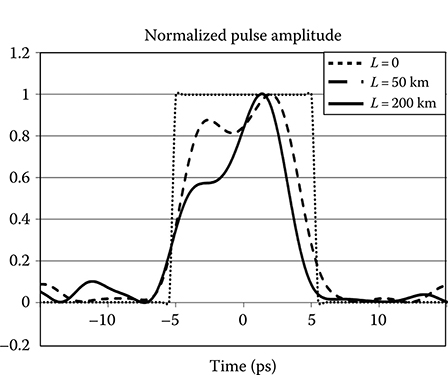
FIGURE 9.2 NRZ pulse at 100 Gbit/s after linear propagation without any PMD. The spectrum is centered on the dispersion zero of the used DS fiber to show the effect of dispersion slope.
In particular, the pulse shape of the 16th channel is reported for a dispersion slope of 0.05ps3/km and different link length. All the pulses are normalized to their maximum amplitude.
The pulse distortion due to the dispersion slope is quite evident, and after 5 km propagation, the greatest part of the transmitted energy is out of the bit interval while the pulse shape is completely destroyed.
This means that dispersion compensation has to be performed channel by channel, taking into account the exact dispersion value in the channel spectral position.
But this is not enough, as shown in Figure 9.2. In this figure, similar to Figure 9.1 for its construction, the center channel of the WDM comb is considered, having the dispersion zero in its center wavelength.
Nevertheless, the fact that the channel spectrum is so wide causes a pulse distortion due to the third order dispersion even if the average dispersion in the channel bandwidth is zero. The intersymbol interference (ISI) caused by third order dispersion is already important after 50 km propagation and after 200 km propagation a relevant quantity of the pulse energy is out of the bit interval.
The need of per channel compensation depends from the width of the NRZ spectrum that is about 200 GHz. Since multilevel modulation shrinks the spectrum of the transmitted signal, it helps to attenuate the penalty dependence on third order dispersion.
As an alternative, or even to integrate the effect of spectrum width reduction, per channel compensation can be applied.
The cheaper method to operate per channel dispersion compensation is to use an electronic equalization circuit. The exact compensation of a precise wavelength behavior of the dispersion coefficient is more difficult if electronic dispersion compensation is used in conjunction with Direct Detection since the nonlinear detector characteristic has to be taken into account. This difficulty is removed if coherent detection is used, due to the complete proportionality of the photocurrent to the optical field, both in amplitude and phase. In this condition, if linear fiber propagation can be assumed, the propagation channel is linear even considering the detector characteristic, thus allowing far more efficient dispersion compensation to be applied.
9.2.2.2 Tunable Optical Dispersion Compensator
A great amount of research has been devoted also to Tunable Optical Dispersion Compensators (TODC) for application at 40 and 100 Gbit/s. A TODC is an optical transparent component that is able to compensate a selectable amount of dispersion (generally with a selected slope) on one or more high speed channels.
TODC are divided into single channel and multiple channels devices, where the first are suitable to compensate a single channel, while a whole WDM comb can be simultaneously compensated by the latter.
Single channel TODC [1] are mainly studied for intermediate reach, very high speed systems, where electronic dispersion compensation is not enough due to the nonlinear characteristics of the photodiode, but cost constraints or other considerations (related for example to real estate or power consumption) render unsuitable coherent detection.
On the other hand, the advantage expected by multichannel TODC is the ability to compensate the dispersion of a whole WDM comb with a single optical device, without the need of demultiplexing the optical channels.
Thus, multichannel TODCs are complementary to the electronic compensation and the most probable solution to deal with chromatic dispersion of large bandwidth optical signals is a contemporary use of TODC for in-line compensation plus electronic fine equalization at the receiver.
This solution, based on periodic compensation along the optical transmission line, has the advantage of avoiding combination between dispersion and nonlinear distortion that unavoidably occurs if all equalization is placed at the receiver and that renders electronic equalization much more difficult and expensive.
In order to be used in this way, the multichannel TODC have to be simple from a design point of view and must be able to compensate the typical amount of dispersion occurring in a long haul system span.
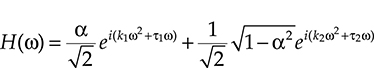
One of the more direct ways to realize a multiple channel TODC is shown in Figure 9.3 and consists in dividing the incoming optical channel between the two branches of an interferometer where two different dispersion elements are placed. The amount of optical power sent in each branch is regulated by a selectable directional coupler [2].
The transfer function of the system is given by
H(ω)=α√2ei(k1ω2+τ1ω)+1√2√1−α2ei(k2ω2+τ2ω)(9.2)
(9.2)
where
ki indicates the coefficient of dispersion of the dispersive elements
τi is the overall delay along the two interferometer branches
α is the tunable splitting ratio, while the factor 1/√2![]() takes into account the unavoidable loss of the beam splitter
takes into account the unavoidable loss of the beam splitter
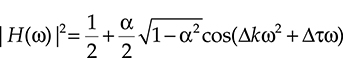
The module of the transfer function writes
|H(ω)|2=12+α2√1−α2cos(Δkω2+Δτω)(9.3)
(9.3)
where Δk = k1 − k2 and Δτ = τ 1 − τ2.
The module of the spectral response of the interferometer is a periodic function, as obvious, whose period is frequency dependent due to the quadratic behavior of the object of the cosine function. The optical bandwidth depends on the frequency dependent term and it is maximum where this term is zero, that is, when α = 0 or α = 1.
On the other hand, the optical bandwidth is minimized when the third term in Equation 9.3 is maximum, that is, α=1/√2![]() .
.
In order to determine the group delay of the interferometer and then the overall dispersion characteristic, the phase contribution Φ(ω) of the response in Equation 9.2 has to be calculated and derived with respect to the angular frequency.

FIGURE 9.3 Block scheme of an interferometric TODC: DE1 and DE2 represents two different dispersion elements.
The result depends again on the factor A(ω) = (Δkω2 + Δτω) that appears under a cosine function.
It is possible to select Δk and Δτ so that in a determined optical bandwidth, the approximation is verified: A(ω) = (Δkω2 + Δτω) = 0.
Assuming to be in this condition, the differential delay expression of the interferometer can be quite simplified, up to arriving at the following expression
dΦdω=(α2+α√1−α2)(k1ω+τ2)+(1−α2+α√1−α2)(k2ω+τ2)2π(1+2α√1−α2)(9.4)

(9.4)
Equation 9.4 has the form expected by a TODC, since it linear in ω and depends on an adjustable parameter, which is α.
Just to make an example, let us consider a fiber interferometer where the dispersion is achieved by fiber brag gratings.
The device parameters are summarized in Table 9.1. From the table it results that the condition of A(ω) = 0 is attained introducing a length difference of about 1.1 μm among the gratings at a wavelength of 1.55 μm. The behavior of cos[A(ω)] is represented in Figure 9.4 versus the wavelength deviation with respect to 1.55 μm.
TABLE 9.1 Physical Parameters of the Fiber Components Used in the Example of Wideband Tunable Dispersion Compensator


FIGURE 9.4 Bandwidth of the response of an interferometric TODC.

FIGURE 9.5 Differential delay versus the wavelength for an interferometric TODC and for different values of the setting parameter α.
The TODC in this example has a bandwidth of about 40 nm around the reference wavelength (corresponding to 1.55 μm) that is a very good bandwidth to operate as multi-wavelength TODC in DWDM systems.
The group delay is shown in Figure 9.5 versus the wavelength deviation for different values of α. The group delay behavior is, in this ideal case, linear with the wavelength with a very good approximation, thus confirming the good performance of this architecture in conjunction with fiber Brag gratings.
Naturally, in practical implementations, several nonidealities affect the behavior of the TODC, like reflectivity of the gratings, ripple in the phase characteristics of the dispersion elements, losses of the whole device, and so on. A detailed analysis of such impairments besides a practical implementation of a compensator and a transmission experiment are presented in [2].
Moreover in [2] it is also shown that a compensator with the architecture of Figure 9.3 can also be used as a single channel compensator coupling the signal directly in the electrical domain. In this case, the compensator is an alternative to electronic compensation.
Several other architectures have been proposed for the TODC, having different characteristics.
A class of compact TODC are based on the use of Array Waveguides (AWGs) [3,4] since these devices provide contemporary demultiplexing and different dispersion contribution channel per channel. Moreover, if suitably designed, the same AWG can be used both for multiplexing and for demultiplexing the DWDM comb increasing the dispersion contribution and gaining in compactness.
An example of AWG architecture is presented in [3] and is reported in Figure 9.6. The component working is quite simple. The incoming optical field is decomposed by the AWG, which divides its spectrum slices, its spectral phase around the center frequency is adjusted by the lens located near the spectral plane, reflected by the mirror, and recombined in the AWG to regenerate the field. Depending on the AWG design, this TODC can be used either to compensate interchannel dispersion due to the dispersion slope in particularly wide spectrum transmissions or multichannel dispersion in WDM systems.
In the first case however, the distortion due to the spectral analysis of the channel and successive composition of the spectral components has to be taken into account. The compensator tuning is performed by using a cooler and exploiting the thermal dependence of the optical characteristics of the silica composing the AWG and the lens structure.
An improvement of the performance of the TODC can be attained by realizing several lenses monolithically integrated into the structure of the chip so that the whole device is a planar silicon on silica-integrated circuit. The characteristics of an experimental realization of the device are reported in Figure 9.7 [3].
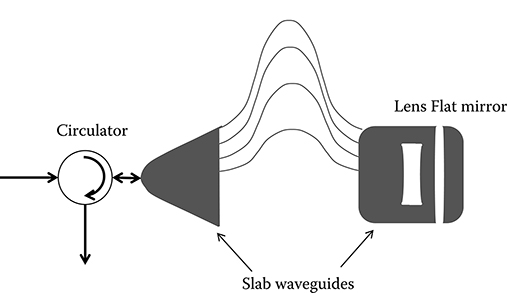
FIGURE 9.6 TODC based on a cyclic AWG.
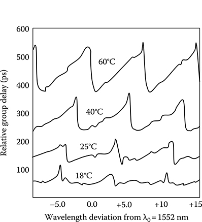
FIGURE 9.7 Differential Delay of the AWG based TODC versus the temperature.
(After Ikuma, Y. and Tsuda, H., IEEE J. Lightwave Technol., 27(22), 5202, 2009.)
Another technology used to implement experimental TODCs is based on discrete optics and on technologies similar that used in 3D Micro Electrical Mechanical machines (MEMs), Liquid Crystal on Silicon (LCOS) switches and in Wavelength Selective Switch (WSS) components (see Chapter 5 for MEMs switches and Chapter 6 for WSS).
An example of TODC using this technology is reported in [5] and its block scheme is shown in Figure 9.8. A circulator deviates the whole DWDM comb into an AWG where the channels are demultiplexed. At the AWG output, a free space optics directs the demultiplexed channels on a bulk grating and, at the grating output, a lens focalizes the channels on an LCOS switch. The LCOS reflects back the channels that traverse the system again in the opposite direction to be reinjected by the circulator into the transmitting fiber after multiplexing by the AWG.
The AWG, the LCOS deflector, and the Brag grating, all provide dispersion and, if the dispersion axis of the grating is orthogonal to that of the AWG and the two dispersion axes of the LCOS are parallel and orthogonal to the AWG axis, it is possible to combine the dispersion contributions to have different dispersions for the different channels.
FIGURE 9.8 Discrete optics TODC based on LCOS technology.
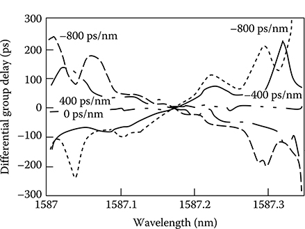
FIGURE 9.9 Differential delay of the LCOS based TODC.
(After Seno, K. et al., 50-Wavelength channel-by-channel tunable optical dispersion compensator using combination of arrayedwaveguide and bulk gratings, Conference on Fiber Communication (OFC), Collocated National Fiber Optic Engineers Conference, 2010 (OFC/NFOEC), San Diego, CA, IEEE/OSA, s.l., 2010, pp. 1–3.)
In the paper where this architecture is proposed [5] the TODC design is performed for application in the L band at 40 Gbit/s.
The measured dispersion performances for a single channel among the 50 that can be simultaneously processed by the device are reported in Figure 9.9 for different driver voltages of the LCOS. The ripple that can be observed in the experimental characteristics is attributed to the imperfect alignment of the LCOS device, a hypothesis that is reinforced by the presence of an analogous ripple in the amplitude transmittance [5]; in any case, the ability of the device to attain a range of dispersion between −800 and 800 ps/nm results clearly from the figure.
9.2.3 Fiber Polarization Mode Dispersion
9.2.3.1 Impact of Polarization Mode Dispersion on 100 Gbit/s Transmission
A first evaluation of the impact of PMD on transmission of high speed channels has been carried out in Chapter 6 and an example of performance evaluation is reported in Figure 6.12 for channels at 40 and at 100 Gbit/s.
Using the parameters of Figure 6.12 (see Table 6.1) it is possible to evaluate the transmission length at which the PMD-induced penalty is 2 dB, that we can call maximum PMD transmission distance. The value of the maximum PMD transmission distance is reported in Figure 9.10 versus the bit rate for different values of the PMD parameter. Dots are values calculated with the model of Chapter 6 and assuming linear propagation. The curves are interpolated with a function inversely proportional to the bit rate through a constant.
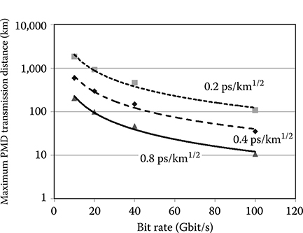
FIGURE 9.10 Maximum PMD transmission distance versus the bit-rate for different values of the PMD parameter.
From the figure it is quite evident that the fit is very good, almost in all the interesting range of values for the PMD parameter.
Thus we can conclude without a big error that the maximum PMD transmission distance is inversely proportional to the bit rate.
From Figure 9.10 it is also clear that the impact of PMD is very important at 100 Gbit/s: the maximum PMD transmission distance for a PMD parameter of 0.2 ps/km1/2 is about 100 km.
Also in this case, since the dependence of the PMD penalty on the bit rate is due to the relationship between the bit rate and the optical bandwidth, both adoption of multilevel modulation and coherent detection are beneficial for the same reasons discussed in the above section.
9.2.3.2 Polarization Mode Dispersion Compensation
PMD can be naturally compensated both electronically and optically. The main issue in PMD compensation is the fact that it is a random phenomenon, thus requiring adaptive compensators to follow its fluctuations.
Electronic compensation circuits generally have such a feature, thus being suitable for compensating PMD, besides other ISI-related impairments like chromatic dispersion. For example, in Figure 5.53, it is shown as both feedforward equalizer/decision feedback equalizer (FFE/DFE) and maximum-likelihood estimation (MLE)-based compensators can reduce the PMD-induced penalty for 10 and 20 Gbit/s signals.
Scaling the bit rate at 100 Gbit/s poses however a great challenge to electronic compensation, due to the great speed at which the compensator has to work.
Even if traveling wave FFE/DFE compensators have been realized and demonstrated as effective in compensating PMD at 40 Gbit/s [6], no electronic equalization has been realized on a serial signal at 100 Gbit/s.
For this reason, optical PMD compensation has a particular importance at very high speed.
As a matter of fact, due to the random nature of the PMD, the instantaneous performance of the system can be also completely ruined by PMD in the occasion of unfortunate fluctuations of the Jones matrix even if the average penalty is quite low.
To understand this phenomenon, let us consider the PMD-related penalty as defined in Figure 6.12: it was evaluated by starting from the error probability for a specific value of the PMD broadening Δτ and averaging with respect to Δτ. It is clear that, while Δτ fluctuates, the system can experience instantaneous values of the penalty either smaller or larger than the average value.
To evaluate the impact of these fluctuations, generally, the so-called outage probability PO is used, that is, the probability that the instantaneous value of the PMD-induced penalty is higher than the value used in the system design, or equivalently (assuming all processes ergodic), the percentage of time in which the PMD-induced penalty is higher than the design value.
In order to approach the problem of reducing the outage probability, it is important to notice that when launching a pulse into a fiber link with PMD, the received pulse width depends on the launched state of polarization (SOP), and in particular on its position with respect to the input Principal States of Polarization (PSPs), following Equation 4.29. The effect of the launched polarization state on the pulse broadening is represented in Figure 9.11 [7] where the pulse spreading ratio β is shown versus the normalized average pulse width α.
The parameters β and α are defined as
β=√1+σ2Δττ2in(9.5)

(9.5)
α=〈τ〉τin

where
τin is the half width at half maximum of the input pulse
〈τ〉 is the average half width at half maximum of the output pulse
σ2Δτ![]() is the variance of the half width at half maximum of the output pulse as defined in Equation 4.29
is the variance of the half width at half maximum of the output pulse as defined in Equation 4.29
Looking at Figure 9.11, it results that there is quite a difference between launching the input pulse along the worst and along the best polarization state. Thus, a way to attenuate the penalty due to PMD via the elimination of the worst cases is simply to apply a fast random polarization scrambling.
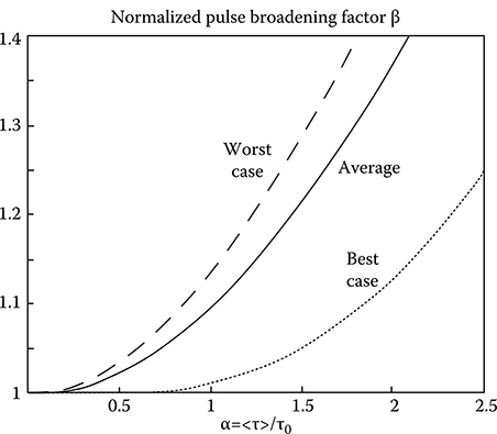
FIGURE 9.11 Dependence of the variance of the pulse width at the output of a PMD affected fiber on the launch polarization state: best, average and worst cases are shown.
(After Sunnerud, H. et al., IEEE Photon. Technol. Lett., 12(1), 50, 2000.)
If the polarization scans almost all the possible states during a bit period, the pulse spreading will be, in a very first approximation, always the average one and the worst cases will be avoided.
In order to evaluate the effectiveness of this method, let us image that the outage probability is PO = 10−3 in the absence of fast polarization scrambling and that, in order to avoid mixing of the PMD effect with self-phase modulation (SPM), we will introduce periodic scrambling along a 300 km long line at 100 Gbit/s with a PMD of 0.1 ps/km1/2 (see Figure 9.11).
The effect on the outage probability of periodic polarization scrambling via equally spaced scramblers placed along the line is shown in Figure 9.12 versus the number of scramblers [8].
Polarization scrambling technique is quite effective in reducing penalty fluctuations due to the random nature of the PMD, with the additional advantage of being able to process a whole WDM comb without demodulation, but while the bit rate increases, it is more and more difficult to perform a perfect scrambling, that is, scramble at a so high speed that almost all the polarizations states are traversed during the bit time. Let us imagine that the scrambling speed is not sufficient, in particular, let us assume that it is 20% smaller than the speed needed to span all the possible states of polarization.
The resulting outage probability is also reported in Figure 9.13 [8] and the result is that, even if the scrambling is much less effective, the outage probability is in any case much smaller than the case without scrambling if a sufficient number of scramblers is used.
The fact that PMD fluctuations induce outage also suggests the fact that errors due to these fluctuations form bursts. In case of transmission channels causing error bursts, the use of specific burst correcting forward error correcting codes (FECs) is quite effective.
Systems using specific FECs and fast polarization scrambling can be optimized to greatly reduce PMD penalty fluctuations up to very low values of the outage probability [9,10].
If the average penalty due to PMD is acceptable from a system design point of view, a reduction of the outage probability below a required lower limit is enough to assure a correct system working.

FIGURE 9.12 PMD related outage probability versus the number of in line scramblers, both ideal and slow scramblers (see text) are considered.
(After Lid, X. et al., Multichannel PMD mitigation through forward-error correction with distributed fast PMD scrambling, Optical Fiber Communication Conference (OFC 2004), Los Angeles, CA, IEEE, s.l., 2004, Vol. 1, pp. WE2 1–3.)

FIGURE 9.13 Block scheme of a first order PMD compensator.
If the average PMD penalty is too high, an effective PMD compensation is needed that is able to reduce both the outage probability and the average penalty. The scheme of a simple PMD compensator, a so-called first order compensator, is reported in Figure 9.13. At the transmission fiber output a Polarization Controller is set to split the signal between fast (→p−)![]() and slow (→p+)
and slow (→p+)![]() PSP components. The components along the PSPs are mutually delayed by the differential group delay (DGD) Δτ and then recombined. The delay is generally obtained by rotating the PSPs to match the axes of a tunable birefringence element.
PSP components. The components along the PSPs are mutually delayed by the differential group delay (DGD) Δτ and then recombined. The delay is generally obtained by rotating the PSPs to match the axes of a tunable birefringence element.
Both the PSP decomposition and the DGD have to be adjusted via an adaptive algorithm to match the slowly varying transmission link characteristic [11–14].
Several algorithms have been devised to simplify the apparent complexity of the PMD compensator and several designs have been presented that are quite effective in perfectly compensating the PMD in the central frequency of the signal spectrum.
Obviously, to compensate a whole WDM comb, it has to be demultiplexed and compensated channel by channel. Thus, a first order PMD compensator like that shown in Figure 9.13 is generally designed to be deployed immediately before detection.
A first order PMD compensator has two main limitations. The first is related to the nonlinear evolution of the signal along very long fiber links. When the linear and nonlinear polarization evolutions are mixed, it is not yet possible to distinguish them and a linear compensator is not yet able to correctly recover the signal [11]. This means that in order to use effectively such compensators, the propagation has to be maintained as linear as possible (but for the soliton case that is considered in detail in [12]).
More important, by increasing the bit rate, the bandwidth of the PSPs starts to be of the order or even smaller than the optical bandwidth of the signal. As a matter of fact, from Chapter 4, we derive that the PSP bandwidth in a Standard Single Mode Fiber (SSMF) if of the order of 100 GHz, while the bilateral optical bandwidth of a 40 Gbit/s NRZ signal is 80 GHz and that of a 100 Gbit/s NRZ signal is 200 GHz.
In such a condition, intrachannel variations of the PSP causes a relevant signal distortion even if a first order PMD compensator is used.
A more accurate compensation can be attained by approximating the PMD with a second order expression in ω instead of a first order one [15] and designing a second order PMD compensator. A possible scheme of a second order PMD compensator is reported in Figure 9.14 [16,17].
The effectiveness of second order compensation is quite improved for high bit rate signals with respect to first order compensation as shown in [18]. A comparison between different first order and second order PMD compensators based on various control algorithms and compensating elements is reported in Figure 9.15 [18] where the outage probability PO is reported as a function of the design average PMD penalty ΔSNe (dB) for a bit rate of 100 Gbit/s, NRZ transmission, and an average PMD-induced DGD of 3.8 ps (deriving, e.g., from a 100 km long link with DPMD = 0.38 ps/km1/2).

FIGURE 9.14 Block scheme of a second order PMD compensator.
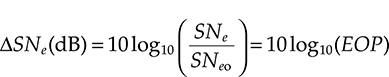
Comparing Figure 9.15 with literature, it is to take into account that the penalty is frequently expressed as instantaneous Eye Opening Penalty (EOP). Since evolution of the PMD is much slower than the bit-time, the PMD DGD can be considered almost constant for a great number of consecutive bits. In this situation, there is a direct relationship between the instantaneous EOP and the SNe penalty once the link characteristics are fixed. As a matter of fact, indicating with I0 and I1 the average values of the photocurrent decision samples corresponding to the two transmitted bits, and with I00 and I10, the same values in the absence of PMD, we can write (see Chapter 6)
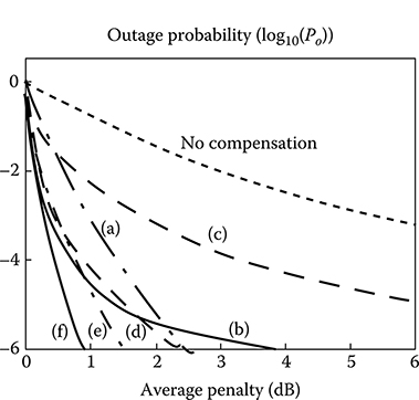
FIGURE 9.15 Comparison between different first order and second order PMD compensators based on various control algorithms and compensating elements. (After Heismann, F., IEEE Photon. Technol. Lett., 17(5), 1016, 2005.) (a) Conventional FO-PMDC with variable differential phase delay. (b) PMDC based on the Kogelnik– Bruyère model described in [19]. (From Kogelnik, H. et al., Opt. Lett., 25(1), 19, 2000.) (c) PMDC based on the truncated EEF described in [20]. (From Eyal, A. et al., Electron. Lett., 35(17), 1658, 1999.) (d) PMDC described by [18]. (From Heismann, F., IEEE Photon. Technol. Lett., 17(5), 1016, 2005.) (e) PMDC formed by two concatenated First Order-PMDCs, wherein the first introduces a fixed DPD equal to the mean DGD in the fiber and the second a continuously variable DPD [21]. (From Yu, Q. et al., IEEE Photon. Technol. Lett., 13(8), 863, 2001.) (f) PMDC described by [19,21]. (From Yu, Q. et al., IEEE Photon. Technol. Lett., 13(8), 863, 2001; Kogelnik, H. et al., Opt. Lett., 25(1), 19, 2000.)
EOP=I1−I0I10−I00(9.6)

(9.6)
SNe=I1−I0σ1−σ0

where σ1 and σ0 are the overall noise variance corresponding to the two transmitted bits.
Assuming that the noise does not change, the following equation is immediately derived:
ΔSNe(dB)=10log10(SNeSNeo)=10log10(EOP)(9.7)
(9.7)
The PMD compensators considered in Figure 9.15 are
Conventional first order-polarization mode dispersion compensation (FO-PMDC) with variable differential phase delay
PMDC based on the Kogelnik–Bruyère model described in [19]
PMDC based on the truncated exponential expansion form (EEF) described in [20]
PMDC described by [18]
PMDC formed by two concatenated First Order-PMDCs, wherein the first introduces a fixed differential phase detector (DPD) equal to the mean DGD in the fiber and the second a continuously variable DPD [21]
The performance of second order compensators depends in an important measure on the control algorithm and on the effectiveness of the compensation device, but it is in any case quite better than the performance of a single order compensator.
The number of stages of the PMD compensator can be increased to three or more in order to achieve high order compensation and target better performances. More compensation stages however also mean a more complex control algorithm and a more expensive device (keeping in mind that PMDCs are per channel devices).
The performance improvement and the control complexity of high order compensation devices have been studied in several papers [22]. An estimation of the possible performance of a third order PMD compensator is reported in Figure 9.16 [22]. When compared to a relevant gain passing from a first to a second order compensator, the gain achieved when passing from a second to a third order component is not so pronounced while it is paid with a sensible increase in the complexity. Thus it is possible to conclude that system design should try as much as possible to use second order compensator (if optical compensation is needed) and passing to third order compensators only if it is really needed.
9.2.4 Other Limiting Factors
9.2.4.1 Fiber Nonlinear Propagation
Increasing the signal bandwidth has essentially no impact both on Brillouin (at least if the carrier is maintained in the spectrum) and on Raman effects.

FIGURE 9.16 Estimation of the possible performance of a third order PMD compensator.
(After Kim, S., IEEE J. Lightwave Technol., 20(7), 1118, 2002.)
While the impact of Cross Phase Modulation (XPM) and Four Wave Mixing (FWM) can be managed by a suitable channel spacing and residual dispersion, SPM depends on the individual channel and can become the dominant nonlinearity and the system limiting factor besides PMD.
In this case also, the reduction of the signal bandwidth occupancy seems to be the only way to go to reduce SPM impact besides the possibility of an effective electronic compensation via some kind of coherent detection or of signal predistortion (compare Chapter 5).
9.2.4.2 Timing Jitter
Due to the very short bit time, timing jitter assumes a particular importance in 100 Gbit/s serial systems. We can decompose the jitter into three factors:
Transmission jitter
Detection clock jitter
Propagation jitter
The transmission jitter depends on the fluctuations of the transmitter clock that causes the center instant of the pulses sent to the modulator to fluctuate randomly around the average value. This problem can be faced with a combination of a local improvement of the clock electronics and a more performing network timing distribution in case synchronous timedivision multiplexing (TDM) is used.
Analogously, the receiver clock jitter depends on the imperfection of the receiver clock electronics that causes the sampling instant before the decision device to fluctuate randomly around the average value. Also in this case, the problem can be faced with a combination of a local improvement of the clock electronics and a more performing network timing distribution.
The propagation jitter is caused by a different phenomenon and affects systems where SPM is partially compensated by a residue chromatics dispersion [23]. This jitter contribution becomes evident for pulses with a full width at half maximum (FWHM) of the order of few ns, that could be used in return-to-zero (RZ) 100 Gbit/s systems.
The propagation jitter is a combination of the jitter due to pulse interaction and to the jitter due to ASE to pulse nonlinear combination.
The first effect is a reduced form of the Gordon-Haus jitter that appears in soliton propagation. This jitter caused by attraction between nearby pulses becomes more and more effective by increasing the Chromatic Dispersion–SPM compensation degree [24,25], and comes into play especially when strong under-compensation of chromatic dispersion is used to counterbalance SPM. The other cause of propagation jitter is the phase noise produced by the nonlinear ASE to signal coupling and it is known as Gordon-Mollenauer effect [26].
9.2.4.3 Electrical Front End Adaptation
A serial 100 Gbit/s signal has a huge bandwidth and it is not easy to device receivers with a low-pass bandwidth of 100 GHz. Distortions in the photocurrent directly affect the receiver performances via ISI and loss of power in the bit interval. Great progress have been made in the last years, but this is yet an important challenge [27].
9.3 Multilevel Optical Transmission
In the previous section we have seen that one of the main problems in NRZ serial transmission of 100 Gbit/s signals is the huge optical spectral width.
The NRZ 100 Gbit/s spectrum is 200 GHz wide (unilateral bandwidth 100 GHz), causing a great amount of ASE noise to enter the receiver and a great sensitivity both to chromatic dispersion slope and to PMD.
Moreover, nonlinear Kerr effect depends also on the signal bandwidth, worsening the problem of transmitting NRZ 100 Gbit/s signals.
Several alternative modulation formats can be used to reduce the 100 Gbit/s spectral width, such as single side band modulation or duobinary modulation (see description and References in Chapter 6), but the most effective and flexible way to reduce signal bandwidth is multilevel modulation [28,29].
In general, multilevel modulation consists in coding the binary signal to be transmitted in a signal that consists of a series of symbols extracted by an alphabet A of M symbols so that the two signals are equivalent under an information point of view.
This means that an invertible code must exist that establishes a correspondence between the input bit stream and the stream of elements from the alphabet A. In this condition, if the stream of transmitted symbols is correctly received, the original bit stream can be univocally reconstructed.
If this is true, it is also possible to evaluate, starting from the correlation function of the bit stream, the resulting correlation function of the symbol stream to be transmitted [30].
In the case of 100 Gbit/s application, all electronic coding and decoding operations have to be carried out by very high speed electronics; thus, it is realistic to restrict the analysis of multilevel modulation to a particular case of modulation formats, allowing simple coding/decoding and modulation/demodulation operations to be performed.
This is the class of the so-called “instantaneous” modulation formats, characterized by the property that, if the incoming bits are statistically independent, also the symbol stream derived from coding is composed of statistically independent symbols.
In general, the multilevel coding is performed by dividing the incoming bit stream in words of n bits and coding each word with a symbol from an alphabet of M = 2n symbols.
Even if this is a particular class of multilevel modulations, it is still sufficiently rich to contain remarkably different modulation formats.
9.3.1 Optical Instantaneous Multilevel Modulation
In Chapter 6, we have introduced the so-called quadrature representation of the single mode electromagnetic field that propagates in an optical fiber.
Let us call →p+![]() and →p−
and →p−![]() two orthogonal unitary polarization vectors (e.g., the output polarization principal states or two orthogonal linear polarizations). In general, once the slowly varying component of the optical field is neglected, the transversal shape that is constant during propagation (see Chapter 4), can be written as
two orthogonal unitary polarization vectors (e.g., the output polarization principal states or two orthogonal linear polarizations). In general, once the slowly varying component of the optical field is neglected, the transversal shape that is constant during propagation (see Chapter 4), can be written as
→E(t)=[e1(t)+ie2(t)]→p+[e3(t)+ie4(t)]→p−(9.8)
![]()
(9.8)
The four real functions ej (t) (j = 1, 2, 3, 4) are the so-called four quadratures of the optical field in the base (→p+,→p−)![]() and they are the independent degrees of freedom that can be exploited to modulate the field.
and they are the independent degrees of freedom that can be exploited to modulate the field.
The optical field power P (t) can be expressed as the sum of the square of the quadratures, that is,
p(t)=e21(t)+e22(t)+e23(t)+e24(t)(9.9)
![]()
(9.9)
Exploiting (9.9), it is possible to introduce the so-called quadrature space, that is, the space having the quadratures as coordinates. This is a Euclidean four dimensional space, where the instantaneous value of the field is represented by a four-vector whose norm is the field power. In this space, the set of field states having the same power are thus spherical surfaces whose radius is the square root of the power itself.
A general instantaneous multilevel modulation of the field can be represented as following
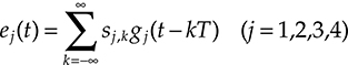
ej(t)=∞Σk=−∞sj,kgj(t−kT) (j=1,2,3,4)(9.10)
(9.10)
where
gj (t) is the pulse used to modulate the jth quadrature
sj,k is one of the set of amplitudes (s1, …, sNj) adopted for the modulation of ej (t), where we can assume that Nj = 2nj , so that
M=N1N2N3N4=2n with n=n1+ n2+n3+n4 (9.11)
![]()
(9.11)
In many practical cases, for example, M-ary Quadrature Amplitude Modulation (M-QAM) and M-ary Phase Shift Keying (M-PSK), the same pulse is used to modulate all the quadratures, thus we will assume this condition and we will neglect the index for gj(t), calling the modulation pulse simply g(t). In any case, it is straightforward to generalize the derivations that follow to the case of different modulating pulses for the different quadratures.
Once a general description of this class of modulation formats is set up, we have first to demonstrate that a practical modulator for such signals can be built and then evaluate the transmitted signal power spectral density to verify the expected shrink with respect to a standard NRZ signal at the same bit rate.
A possible scheme of a modulator for a general modulation format of this class is reported in Figure 9.17.
This is a cascade of an amplitude, a phase, and a polarization modulator [31]. It is clear that in practice, when particular modulation formats are adopted, this will not be the optimum modulator and other schemes will be used. Just to consider only one aspect, the modulators cascade causes a great loss to be introduced on the field to be transmitted.
However, the scheme of Figure 9.17 demonstrates that whatever modulation format of this class is considered, a possible modulation scheme exists.
As far as the spectrum occupation is considered, we can define the so-called optical field spectrum matrix S in the base (→p+,→p−)![]() through its elements as
through its elements as
sh,j(ω)=ℑ{〈sj,kg(t−kT)sh,k′g(t−k′T)〉}(9.12)
![]()
(9.12)
where
ℑ() indicates the Fourier transform
<x> indicates the ensemble average
Since the pulse g(t), in order not to provoke ISI, is completely contained in the symbol interval and due to the independence among symbols transmitted in different intervals, (9.12) rewrites
sh,j(ω)=〈sj,ksh,k〉ℑ{|g(t)|2}=G(ω,T)〈s2j,k〉δj,h(9.13)
![]()
(9.13)
where
G (ω, T) is the power spectral density of the transmission pulse
〈s2j,k〉![]() is the average of the square of the transmitted symbols
is the average of the square of the transmitted symbols
δj,h is one if j = h, otherwise it is zero

FIGURE 9.17 Block scheme of the generic modulator for instantaneous multilevel modulation formats.
The power spectral density S+(ω) and S−(ω) of the two polarization components of the transmitted signal (9.8) can be evaluated starting from the elements of the matrix S. In the hypothesis of instantaneous modulation, from Equation 9.13 it is deduced that S is always a diagonal matrix so that
S+(ω)=S1,1(ω)+S2,2(ω)=S0+G(ω,T)S−(ω)=S3,3(ω)+S4,4(ω)=S0−G(ω,T)(9.14)

(9.14)
where
S0+=〈s21,k〉+〈s22,k〉S0−=〈s23,k〉+〈s24,k〉
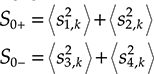
T = n/R, where R is the bit rate and n is defined by Equation 9.11
In the particularly important case of NRZ modulation, g(t) is a square pulse and (9.14) becomes
Su(ω)=S0un2πRsin2(nω/R)(nω/R)2 u∈(+,−)(9.15)

(9.15)
This is quite a common form of an NRZ signal, whose spectrum width is equal to Bo = 2R/n thus confirming the rule anticipated in Section 9.1 for the spectral width of an instantaneous multilevel modulation.
9.3.2 Practical Multilevel Transmitters
Almost in any practical case, the transmitter depicted in Figure 9.18 has a too high insertion loss and practical modulation formats are also selected on the ground of the possibility of designing a low loss–high efficiency modulator.
In this section, we will present a few particular modulation formats that are important in practice.
9.3.2.1 Multilevel Differential Phase Modulation (M-DPSK)
This is probably one of the simpler cases that generalize to multilevel transmission binary differential phase shift keying (DPSK) that we have introduced in Chapter 6: the phase of the transmitted signal is modulated using multilevel differential modulation. Let us call wj the jth world of n transmitted bits and Δθ = 2π/2n .
The M-DPSK signal transmitted in the kth symbol interval and modulated with wj writes
→E(t,k,wj)=√P0eiθ(k)ηT(t,k)→p+(9.16)
![]()
(9.16)
where ηT(t,k) is the Heaviside function that is equal to one for t ε (k − 1)T, kT) and zero elsewhere and θ(k) − θ(k − 1) = jΔθ.
As in the binary case, the name differential comes from the fact that the transmitted symbol is encoded into the phase difference between signals in two consecutive symbol intervals.

FIGURE 9.18 Dual driver Mach–Zehnder modulator used to obtain a multilevel DPSK signal.
In terms of quadrature components, (9.16) writes
e1(t)=√P0cos[θ(k−1)+jΔθ]ηT(t,k)e2(t)=√P0sin[θ(k−1)+jΔθ]ηT(t,k)e3(t)=e4(t)=0(9.17)
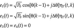
(9.17)
Equation 9.17 shows that the points representing the transmitted symbols in the quadrature space are all distributed on a circle on the e3, e4 plane whose center is in the origin and whose square radius is the transmitted power, which is constant due to the pure phase modulation.
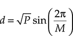
A typical characteristic of a multilevel constellation is the minimum distance d in the quadrature space between a couple of symbols. It is quite intuitive that this distance will be related to the noise robustness of the modulation format. Considering for example binary IM, the constellation is done by two points and the distance is d=√P![]() , so that we can write SNo = d 2/PASE, where PASE is the ASE power.
, so that we can write SNo = d 2/PASE, where PASE is the ASE power.
In this case, we have simply
d=√Psin(2πM)(9.18)
(9.18)
A practical transmitter for the M-DPSK signal is presented in Figure 9.18, conceptually, this is simply a phase modulator, in practice almost only dual drive integrated modulators are used to reduce distortions (see Chapter 5).
9.3.2.2 Multilevel Quadrature Amplitude Modulation (M-QAM)
This modulation format is widely used in radio applications and consists in the amplitude modulation of the two complex quadratures of one of the field polarizations.
The points representing the states of the transmitted field in the quadratures space are comprised in one coordinate plane and form a square lattice: a few examples are provided in Figure 9.19.

FIGURE 9.19 Examples of squared QAM constellations.
In terms of quadrature, the components of the transmitted field can be written as
e1(t)=√P0s1,kηT(t,k)e2(t)=√P0s2,kηT(t,k)e3(t)=e4(t)=0(9.19)

(9.19)
where sj,k is the amplitude of the symbol transmitted along the jth quadrature in the kth symbol interval.
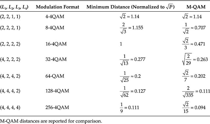
The maximum distance of QAM modulation depends on the adopted pattern and it can be easily evaluated starting from the fact that the power of an optical field is the square of its distance from origin. The minimum distance for a few common QAM patterns is reported in Table 9.2.
A general scheme for an optical M-QAM modulator is reported in Figure 9.20: a laser emits a linearly polarized optical field that is divided into two fields with a phase difference equal to π by a directional coupler. Each field is independently modulated by an amplitude modulator and then one of them is delayed to introduce a further phase difference of π/2. At that point, the two fields are combined again by a directional coupler that introduces a further phase difference of π, so that the total phase difference if 2π + π/2 and the two combined fields are exactly the quadratures of the M-QAM signal.
Such a scheme is suitable to be integrated in a single optical chip, for example, using lithium-niobate or indium phosphide (InP) technology.
Several different modulators have been proposed for particular M-QAM constellations. An interesting scheme is that of the hybrid modulator for 64-QAM proposed in [32]. The principal scheme of the modulator is shown in Figure 9.21 besides the way in which the 64-QAM constellation is formed in the different stages of the modulator. The fact that the modulator is composed of a parallel of three dual drivers phase modulators that has to be driven to produce a four-level phase modulated signal renders the modulator control easy and the loss relatively small.
TABLE 9.2 Normalized Constellation Minimum Distance for M-QAM

The most interesting property of this modulator is, however, that it can be realized by using hybrid integration with two Silica on Silicon chips and a modulator array composed of three phase modulators (let us remember that the modulator of Figure 9.21 is only apparently simpler, since each amplitude modulator is in reality a couple of phase modulators on the branches of an interferometer). The scheme of the hybrid integrated chip is reported in Figure 9.22 where the Silica on Silicon chips are in white and the Lithium–Niobate chip is in gray.

FIGURE 9.20 Block scheme of an M-QAM modulator.

FIGURE 9.21 Architecture of a hybrid modulator for 64-QAM realized with a parallel of three phase modulators.

FIGURE 9.22 Scheme of the layout of a hybrid Si-SiO2 and Lithium Niobate-integrated optical circuit for the implementation of the modulator represented in Figure 9.20.
(From Yamazaki, H. et al., IEEE Photon. Technol. Lett., 22(5), 344, 2010.)
With the same technology, also other kinds of multilevel modulators has been designed and prototyped, like a 16-QAM modulator [33] and a 4-DPSK modulator [34] demonstrating its flexibility.
9.3.2.3 Multilevel Polarization Modulation (M-PolSK)
This modulation format exploits the property of the optical field to be polarized to switch the field polarization among a certain number of states that represents the transmitted symbols. In order to represent optical field states with the same power and phase, but with different polarization in the quadrature space it is needed to represent the surface defined by the following equations:
e1(t)=√Pcos(α)cos(θ)e2(t)=√Pcos(α)sin(θ)e3(t)=√Psin(α)cos(θ+φ)e4(t)=√Psin(α)sin(θ+φ)(9.20)

(9.20)
where the three angles φ and θ define the field polarization. Naturally, the surface is a part of a three-sphere due to the characteristic of the fields described by Equation 9.20 to have the same power. In particular, it is that part corresponding to all the points with the same absolute phase.
Due to the characteristics of this surface, it is not so easy to use quadrature representation to describe polarization modulation.
In optics however, when there is the need for describing the polarization evolution, the Stokes parameters representation is frequently used.
The Stokes parameters are defined as
S1=e21(t)+e22(t)−e23(t)−e24(t)S2=2e1(t)e3(t)+2e2(t)e4(t)S3=2e1(t)e4(t)−2e3(t)e2(t)(9.21)

(9.21)
It is easy to verify that, for a monochromatic perfectly polarized beam it is
P2(t)=S21(t)+S22(t)+S23(t)(9.22)
![]()
(9.22)
so that the SOP of a field can be represented as a point in the so-called Stokes space, which is an Euclidean three dimensional space having the three Stokes parameters as coordinates. In this space, the equal power surface is again a sphere, as in the quadrature space, but the sphere radius in this case is equal to the square of the field power. The sphere of normalized radius (assumed to be equal to one) in the Stokes space is called the Poincare sphere.
The position on the Poincare sphere of the main SOPs are shown in Figure 9.23.
These positions can be derived easily by rewriting the Stokes parameters expressions using spherical coordinates in the Stokes space as follows
S1=Pcos(2Φ)cos(2θ)S2=Psin(2Φ)cos(2θ)S3=Psin(2θ)(9.23)
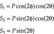
(9.23)

FIGURE 9.23 The Poincare sphere and the position of the main states of polarization.
The angular coordinates in the Stokes space, if defined as in Equation 9.23 and in Figure 9.23 are related to the angles determining the form of the polarization ellipse as shown in Figure 9.24 as it is possible to demonstrate starting from the definition (9.23) of the Stokes parameters.
From (9.23) and the angles definition of Figure 9.24, the position on the Poincare sphere of any SOP can be individuated.
Up to now we have supposed the field completely polarized, as an M-PolSK signal at the output of the modulator.
During propagation however, ASE is added to the field. The noise is randomly distributed among the two polarizations, thus introducing a field depolarization. In this case, the polarization degree can be defined as
σ2p=s21(t)+s22(t)+s23(t)P2<1(9.24)

(9.24)
Where P is the overall field power and the definition of the Stokes parameters becomes
S1=Pσpcos(2Φ)cos(2θ)S2=Pσpsin(2Φ)cos(2θ)S3=Pσpsin(2θ)(9.25)
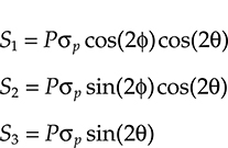
(9.25)
If the light is composed of a fraction of perfectly polarized light and a fraction of perfectly depolarized light (like a PolSK signal plus ASE noise), the power of the polarized component Pp and the power of the unpolarized component Pu are given by
Pp(t)=P(t)σp=√S21(t)+S22(t)+S23(t)(9.26)
![]()
(9.26)
Pu(t)=[P(t)−Pp(t)]=P(t)(1−σp)(9.27)
![]()
(9.27)
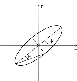
FIGURE 9.24 Relations between the angular coordinates in the Stokes space and the angles defining the polarization ellipse in the physical space.
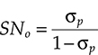
so that, if the Optical SN coincides with the ratio between the polarized and the unpolarized part of the field, it can be written as
SNo=σp1−σp(9.28)
(9.28)
The general instantaneous multilevel Polarization modulation format (M-PolSK: Multilevel Polarization Shift Keying) is obtained by choosing a constellation on the Poincare sphere and associating to each of the constellation points a transmitted symbol.
We will introduce in the following a Stokes parameters receiver for the M-PolSK [35] that can be demonstrated to be the optimum receiver for this type of modulation format [36]. We will see that, also in this case, what is relevant to evaluate the effectiveness of the constellation is the minimum distance in the Stokes space.
Limiting our analysis to constant power modulation, the problem of determining the best possible constellation can be formulated as the problem of distributing M points on a sphere so that the minimum distance between two of them is maximized.
This problem is not easy to be solved analytically and, as far as I know, there is no closed form solution for a generic number of points. A numerical solution for M = 4, 8, and 16 is presented in [37] where both the angular coordinates indicating the position of the points on the Poincarè sphere and the normalized distance matrixes are reported.
The optimum constellations are in a certain sense regular, but do not reproduce the vertices of polyhedrons or other known tridimensional forms. On the other hand, in [36] regular constellations are proposed for M-PolSK.
Considering the vertices of regular polyhedron in the space, the possible M-PolSK formats the minimum distance in the Stokes space and the minimum distance for the optimum configuration with the same number of points are listed in Table 9.3.
TABLE 9.3 Minimum Normalized Distance in the Stokes Space for the Configurations Derived from Regular Polyhedron in the Stokes Space and the Minimum Distance for the Optimum Configuration with the Same Number of Points

a There are four Archimedean solids with 60 vertices and the snub Dodecahedron is the best under a minimum distance point of view.

FIGURE 9.25 Two of the Archimedean solids used to build high order M-PolSK constellations. In the figure, both the plane development and a perspective three dimensional drawing are represented.
To construct regular constellations, Pythagorean and Archimedean solids are used as appropriates to achieve a given number of symbols. When several such solids exist with the same number of vertices, the best from the minimum distance point of view is selected [38,39].
Two of the less known regular solids cited in Table 9.3 are represented both in plane development and in tridimensional representation in Figure 9.25.
For the only three cases in which the optimum constellation is approximately known, it is evident that the gain in terms of minimum distance is relatively small. This will bring us to consider from now on the regular configurations listed in Table 9.3.
For each regular constellation, the power spectral density of the transmitted signal along two reference orthogonal polarizations can be evaluated with standard methods and the complete expression is reported in [37].
The way in which the transmitted power is divided among the two polarization components depends obviously on the choice of the polarization reference frame and, if the field at the output of a transmission fiber is considered, on the fiber instantaneous Jones matrix.
However, the power spectral density in any case exhibits a central zone comprised between the first two spectrum zeros, which are always symmetric with respect to the origin, where almost 92% of the power is comprised. The two considered zeros are at ω = ± 2πR/M thus confirming also for M-PolSK the general rule that the unilateral optical bandwidth can be assumed equal to Bo = R/M so that the spectrum width is 2R/M.
Under the point of view of modulation feasibility, a simple polarization modulator is needed to produce a PolSK signal. A polarization modulator can be realized using electro-optics materials exactly the same way a phase modulator is realized (see Chapter 5) [36,40].
Polarization modulation can be also implemented in conjunction with differential encoding. In this case, the information is coded into the change of the polarization vector in the Stokes space between two adjacent symbol intervals [41,42].
This further coding does not alter the structure of the transmitter, but for the addition of the differential encoder, and in a few cases is quite useful to simplify the receiver.
9.3.2.4 Multilevel Four Quadrature Amplitude Modulation (M-4QAM)
This modulation format exploits the possibility of modulating all the optical field degrees of freedom. The generic M-4QAM signal can be written as
e1(t)=√P0s1,kηT(t,k)e2(t)=√P0s2,kηT(t,k)e3(t)=√P0s3,kηT(t,k)e4(t)=√P0s4,kηT(t,k)(9.29)

(9.29)
where sj,k is the amplitude of the symbol transmitted along the jth quadrature in the kth symbol interval.
A set of constellations for M-4QAM can be obtained simply replying on the two coordinates couples corresponding to the two polarizations the reference constellations of M-QAM.
It is not difficult to demonstrate that this procedure does not produce the optimum constellations from a minimum distance point of view, but is useful to simplify the modulator, that in this case is really a key issue.
As a matter of fact, if these configurations are chosen, the M-4QAM signal can be obtained by a modulator with the block scheme reported in Figure 9.26, which is constituted by two parallel M–QAM modulators.
Since M-QAM modulators can be built as in Figure 9.22, the same technology can be used for M–4QAM modulators.

FIGURE 9.26 Block scheme of a M-4QAM modulator composed of two parallel M-QAM modulators. This modulator scheme is mainly suitable for modulation formats where the constellation is the combination of two squared QAM constellations.
If such regular constellations are chosen, the normalized amplitudes sj,k of the four quadratures are extracted from four sets Xj whose elements can be expressed as a function of four integers numbers Lj and four indices hj, as follows:
sj,k∈Xj≡{(2hj−Lj−1):hj=1,2,...,Lj} j=1,2,3,4(9.30)
![]()
(9.30)
It is clear that, from (9.30) it derives
M=4Πj=1Lj(9.31)

(9.31)
and that the ratio between the minimum distance d and the transmitted power P of a M-4QAM constellation is given by
√P=d√(L1−12)2+(L2−12)2+(L3−12)2+(L4−12)2(9.32)

(9.32)
A few key parameters of some M-4QAM formats of this class are summarized in Table 9.4. For comparison, in the table data relative to M-QAM are also reported. It results that using M-4QAM is always advantageous, but the gain gets smaller and smaller while M increases if squared configurations are used. Just as an example, for M = 16 the gain of squared 16-4QAM versus 16-QAM is 3.2 dB while it is reduced to 0.7 dB if M = 256.
If it is important to gain as much as possible from the constellation points distribution a better constellation has to be selected.
A great amount of work has been done by mathematicians to study forms and properties of four dimensional constellations [43,44].
TABLE 9.4 Minimum Normalized Distance in the Quadrature Space for Squared M-4QAM Constellations
M-QAM distances are reported for comparison.
In the particular case of constant power modulation we can use to define the M-4QAM constellations the vertices of convex, regular polyhedrons in four dimensions, as defined in [45]. Table 9.5 reproduces the structure of Table 9.4, but using the new M-4QAM constellations.
Even better results can be achieved with a careful optimization of more complex constellations [46,47].
It is out of the scope of this book to discuss in detail all the implications of the optimum choice of a four dimensional constellation, here we simply limit ourselves to a few examples based on a simple principle: creating a dense lattice of points via the Cartesian product of bidimensional QAM constellations and then select a subset of points for the final four dimensional constellation.
We will use a simple rule to construct our constellation as the Cartesian product of partitioned QAM constellations in which points are alternatively taken and discarded. An example of this kind of constellation is reported in Figure 9.27, where the generic M-QAM constellation is divided into two partitions: gray points that are taken as components in the (e1, e2) plane and black points that are taken as components in the (e3, e4) plane.
TABLE 9.5 Minimum Normalized Distance of Constant Power M-4QAM Constellations Obtained from the Vertices of Four Dimensional Regular Polyhedrons
Polyhedron |
Modulation Format |
Minimum Distance (Normalized to √P |
M-QAM |
16 Tetrahedral |
8-4QAM |
√2≈1.414 |
1√2≈0.707 |
8 Hexahedral |
16-4QAM |
1 |
√23≈0.471 |
24 Octahedral |
24-4QAM |
1 |
|
600 Tetrahedral |
120-4QAM |
2√5+1≈0.618 |
|
120 Dodecahedral |
600-4QAM |
√2√5+3≈0.270 |


FIGURE 9.27 Partition of a square M-QAM constellation to form by Cartesian product an efficient M-4QAM constellation. Gray and black points individuates the two partitions used to build the final constellation.
TABLE 9.6 Minimum Normalized Distance in the Quadrature Space for M-4QAM Constellations Obtained by the Cartesian Product of Regular Partitions of Squared QAM Constellations
QAM Sub-Set Number of Points |
Modulation Format |
Minimum Distance (Normalized to √P |
M-QAM |
8 |
64-4QAM |
0.4 |
0.202 |
18 |
324-4QAM |
0.329 |
|
32 |
1024-4QAM |
0.286 |
0.046 |
The minimum distances relative to the constellations that are built with this algorithm are reported in Table 9.6.
The results reported in Tables 9.4 through 9.6, besides the outcome of Equation 9.18 for M-DPSK are compared in Figure 9.28. An interesting observation emerges from this figure, which is useful to guide the decision about the number of levels to select when designing a multilevel system based on quadrature modulation. Increasing the number of available degrees of freedom passing from M-QAM to constant power M-4QAM to full M-4QAM is effective in maintaining an high distance among constellation points at high number of levels, while if the number of levels is low, a constellation with a lesser number of degrees of freedom can perform sufficiently well.
9.3.3 Multilevel Modulation Receivers
Since all possible optical field modulation formats can be seen as modulations of one or more of the field degrees of freedom, a receiver that is able to detect all the field quadratures is a universal receiver for optical modulated fields.
Since the quadratures have to be detected with their own sign, to distinguish points in similar positions, but in different quadrants in the quadrature space, coherent detection is needed. This is performed by beating the incoming signals with a local laser (called local oscillator [LO]) at a slightly different wavelength to obtain an intermediate frequency signal that can be processed with standard intermediate frequency (IF) electronics.
This has also the advantage of allowing very effective electronic compensation of fiber propagation effects, first of all polarization fluctuations.

FIGURE 9.28 Comparison on different modulation formats based on quadrature modulation on the ground of the minimum distance between couples of points.
Naturally, this will not be the optimal receiver for all the cases, and sometimes, better performances could be achieved with receivers tailored specifically for the considered modulation format.
This is the case of both M-DPSK and M-PolSK, where better receivers can be designed with respect to the universal receiver.
On the other hand, the quadrature receiver can be demonstrated to be the optimum receiver for both M-4QAM and M-QAM modulation formats, independently from the chosen constellation [28].
Thus, in this section, we will first describe the universal quadrature receiver and then specific optimal receivers for M-DPSK and for M-PolSK.
9.3.3.1 Four Quadrature Receiver
The block scheme of the four quadrature receiver is reported in Figure 9.29. The scope of the receiver is to detect the transmitted quadrature vector for each symbol interval and compare it with the constellation in the symbol space to produce an estimate of the transmitted symbol.
The receiver is divided into two sections: an optical front end (depicted in Figure 9.29a), whose scope is to detect the received field quadratures, and an electronic processing stage (whose architecture is reported in Figure 9.29b), whose scope is to invert the effect of fiber propagation to reconstruct the transmitted field.
A key component in the optical front end is the π/2 optical hybrid that is used, after the separation of the incoming field linear polarization components, both to insulate the quadratures of each polarization and to combine the LO with the incoming field before balanced detection.
Optical hybrids has been produced with several technologies [48–50] and their performances are quite good and stable.
The four fields →Ej(j=1,2,3,4)![]() obtained after polarization splitting and branching with π/2 hybrids can be written as
obtained after polarization splitting and branching with π/2 hybrids can be written as
→Ej(t)=[ξj(t)+ηj(t)→κ(t).→ζj]→ζj(9.33)
![]()
(9.33)
where the information bearing quadratures are indicated with ξj(t) and the ASE optical noise quadratures with ηj(t). The linear polarization unitary polarization vectors directed along the quadrature space reference axes are indicated with →ζj(j=1,2,3,4)![]() while the ASE polarization vector, that is a fast function of time due to ASE complete depolarization, is indicated with →κ(t)
while the ASE polarization vector, that is a fast function of time due to ASE complete depolarization, is indicated with →κ(t)![]() . Finally “.” indicates the scalar product.
. Finally “.” indicates the scalar product.
The field emitted by the LO at π/4 with respect to the local receiver axis is divided into its polarization components by a polarization beam splitter and coupled with the received field components by a set of four π/2 optical hybrids.
In a practical receiver, the set of hybrids can be substituted by a single monolithic hybrid realized in silica on silicon technology. A possible architecture for such a hybrid is shown in Figure 9.30.
Also the set of eight PIN Photodiodes that are needed to realize four balanced receivers can be realized with a diode bar in a single package so that the cost is not eight times the cost of a PIN diode but, for high volumes, could be less than two times.
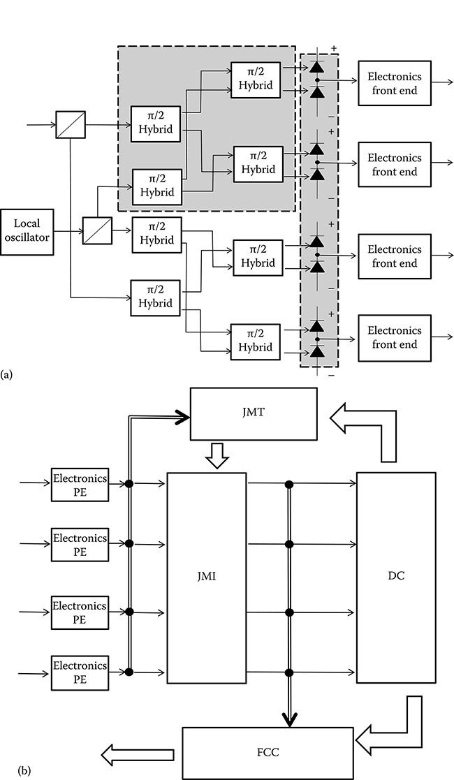
FIGURE 9.29 Block scheme of the quadrature coherent receiver: (a) optical front end; (b) electronic processing. In the optical front end, the gray part can be integrated in an integrated optics circuit: a monolithic Si-SiO2 chip for the hybrids and an InP chip the photodiodes array.

FIGURE 9.30 Schematic layout of the hybrids Si-SiO2 chip. (a) Represents the functional scheme of the chip and (b) a simplified layout.
At the exit of the balanced receivers, the four photocurrents are modulated at the intermediate frequency Δω and further electronic demodulation allows the four field quadratures to be derived.
In order to allow this operation to be performed with high performances, the intermediate frequency Δω has to be stabilized. This can be achieved by a frequency lock loop driven by the wavelength of the incoming signal [31,51].
If the LO frequency is exactly locked to the frequency of the incoming signal the IF demodulation is not needed and the photocurrents are directly in baseband. In this case, the coherent receiver is called homodyne [31].
Under a processing point of view, heterodyne receiver is more complex, but it has been used in radio frequency systems for a long time to alleviate the difficulty of designing wideband components with a very low low-pass frequency (ideally working up to continuous wave [CW]). In optical receivers, heterodyne detection was proposed for the same reason when coherent receivers was first proposed.
With the progress of electronics and with the possibility of digital design also for analog functions, this difficulty is no more so important and the simple homodyne structure seems preferable.
For this reason, up to now we will assume Δω = 0. In this case, the electronics front end reduces to a baseband filter fixing the electrical bandwidth Be ≈ RS of the receiver, RS being the symbol rate, not differently from the case of a direct detection receiver.
The photocurrents in the homodyne receiver have the following expressions:
cj(t)=2RPL[ξj(t)+ηj(t)]+RP2L+R[ξj(t)+ηj(t)]2+nj(t)+ρj(t)(9.34)
![]()
(9.34)
where
R is the photodiodes responsivity, which is assumed to be the same for all the photodiodes
PL is the LO power, which can be written as PL (t) = PL0 [1 + r (t)] if the LO RIN r (t) has to be considered (see Chapter 5)
nj(t) is the shot noise component coming from the jth receiver
ρj(t) is the thermal noise component coming from the jth receiver
If the coherent receiver has to work with the best performances, the LO power has to be much higher both of the incoming signal power and of the so-called “thermal” power. The thermal power is defined as the optical power that would cause a photocurrent with a power equal to the thermal noise power.
The second condition is generally easily realized, while the first could impose limitations on the amplification of the receiver preamplifier.
In these conditions, Equation 9.34 can be simplified as
cj(t)=2RPL[ξj(t)+ηj(t)]+nj(t)(9.35)
![]()
(9.35)
Moreover, due to the fact that a complex electronic processing has to be performed after filtering, we will assume that all electronics functions will be performed via digital circuits. This requires a sampling of the baseband signal before filtering at a sufficiently high sampling rate. On the ground of the experience in electronic compensation, we will assume that five samples per pulse are sufficient to allow effective electronic processing and we will assume a sampling rate Re ≈ 5RS.
This means that in order to work at 100 Gbit/s with a 64-4QAM, the sampling rate has to be about 83 GHz, a very challenging speed, but probably within the reach of very high speed complementary metal–oxide–semiconductor (C-MOS) 22 nm application-specific integrated circuits (ASICS).
Increasing the number of levels, in order to transmit 100 Gbit/s using 512-4QAM with constant power (obtained by selecting 512 levels from the 600-4QAM reported in Table 9.4), the required sampling rate goes down to about 55 GHz, a speed of the order of that used in experimental systems with electronic nonlinear precompensation (experiments with sampling rates around 50 GHz are reported as an example in Chapter 6).
After baseband filtering, the four photocurrents are proportional to the quadratures of the field arriving at the receiver, but for the shot noise contribution.
A part the ASE noise, the quadratures of the received field, is related to the transmitted field quadratures by the fiber propagation characteristics causing chromatic dispersion, polarization rotation and PMD, and nonlinear distortions.
Let us assume in a first moment that fiber propagation is perfectly linear.
The role of the electronic postdetection processing is to compensate as much as possible linear propagation effects to recover the transmitted signal quadratures, to drive the frequency lock of the LO, and to estimate the transmitted symbol.
These functions can be recognized in the scheme of Figure 9.29b, where fiber-induced polarization rotations are compensated by multiplying the received quadratures by the inverse of the fiber polarization rotation matrix (the Jones matrix) in the Jones Matrix Inversion (JMI) block, and pulse distortion by residual chromatic dispersion and PMD are compensated via the Pulse Equalizer (PE).
The Jones matrix evolution at the first order (i.e., without the ω dependence that causes PMD) is tracked by the Jones Matrix Tracking (JMT) block, while the frequency lock loop driving signal is generated by the Frequency Control Circuit (FCC); finally the transmitted symbol is estimated by the Decision Circuit (DC).
The key elements of the electronic section of the receiver are the JMT and the FCC; electronic techniques to compensate linear pulse distortions are already reviewed in Chapter 6, and nothing more has to be added here for this particular case, while Decision Strategies in the general case of a multilevel signal will be discussed in Section 9.4.
9.3.3.1.1 Jones Matrix Tracking Circuit
Since propagation is assumed linear, Equation 4.8 describes the fiber propagation so that the transmitted and the received quadratures are related by the following equation:
[ζ1(ω)+iζ2(ω)ζ3(ω)+iζ4(ω)]=eiδ(ω)[mxx(L,ω)myx(L,ω) mxy(L,ω)myy(L,ω)][e1(ω)+ie2(ω)e3(ω)+ie4(ω)]+[η1+iη2η3+iη4](9.36)

(9.36)
where the fiber link length has been indicated with L and the residual dispersion after the online dispersion compensation is indicated with δ(ω).
The elements mi,j(L, ω) of the Jones matrix are random complex numbers that fluctuates very slowly with respect to the modulation rate and that are related one with the other by the property of the Jones matrix to be unitary. Exploiting the property that the square norm of an optical field is invariant after a transformation with the matrix M, that is, the optical energy is invariant to polarization rotations, it is easy to demonstrate that M depends only on three independent parameters and that it can be rewritten as follows (35):
M=⌊mxx(L,ω)mxy(L,ω)myx(L,ω)myy(L,ω)⌋=[εeiϑ√1−ε2eiφ−√1−ε2e−iφεe−iϑ](9.37)
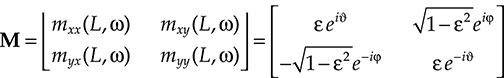
(9.37)
=⌊cos(α)eiϑsin(α)eiφ−sin(α)e−iφcos(α)e−iϑ⌋

The third expression of the Jones matrix, depending on three independent angles (α, ϑ, φ) clearly express the fact that linear polarization evolution can be represented as a rotation in the quadrature space.
The polarization rotation compensation algorithm implemented in the block JMI simply multiplies the input filed quadrature vector by the inverse of M (i.e., equal to M+ since it is a unitary matrix). The first estimate of the matrix M is performed during the system initialization phase by transmitting a field periodically switching among two orthogonal polarizations and observing the field at the output of the receiver.
Once the Jones matrix estimate is initialized, it is updated every TU seconds by the algorithm implemented in the block JMT.
The update interval is also determined in the initialization phase and it has to be at least 10 times shorter than the typical polarization fluctuations time Tp and at least 106 M times longer than the symbol interval.
The interval Tp is defined as the minimum time interval needed to change at least one of the output quadratures of 1% when the field at the system input is constant.
The requirement TU > 106 M assures that, since the symbols are assumed statistically independent and equally probable, averaging over this interval the quadratures of the received field, the obtained value has a Gaussian distribution with a standard deviation about three orders of magnitude smaller that the average [52].
The requirement Tp > 10 TU assures that the fluctuations of M are tracked by the algorithm with a small tracking error.
In real 100 Gbit/s transmission systems, the symbol interval is generally smaller than 100 ps, while Tp ranges from hundreds of milliseconds to minutes [53–55] depending on the type and collocation of the fiber cable, on the season, and similar factors.
An update time TU of the order of 100 μs is thus suitable to assure independency from the modulation and very precise JMT.
The update algorithm works as follows. The constellation points are divided in three categories C1, C2, and C3 constituted by almost the same number of points.
At every point of the category Cj (j = 1, 2, 3) let it call Pj,i (i = 1, …, n1) a rotation matrix is associated, let it call Rj,i, which rotates the reference frame in the quadrature space to transform the coordinates of Pj,i in the reference point Πj.
The coordinates of the reference points are
Π1=(1,0,0,0)Π2=(0,1,0,0)Π3=(0,0,1,0)(9.38)

(9.38)
These matrixes depend only on the chosen constellation and are stored in a look-up table.
Every time a symbol is received, a quadrature vector [ζ1, ζ2, ζ3, ζ4] is present at the input of JMT. In correspondence to these quadratures, the DC produces an estimate of the transmitted symbol and passes it to the JMT. The JMT uses this estimate to associate to the received quadrature vector a matrix Rk,i.
At this point the JMT circuit multiplies the vector X = [ζ1, ζ2, ζ3, ζ4] by Rk,i obtaining an estimate of the position of the reference point Πk.
These estimates are averaged in the time TU to eliminate almost completely the effect of the ASE noise and of the modulation. An average estimate of the positions of the reference vectors Πk is thus obtained. This estimate, that we call 〈RX〉k, depends on the differential rotation happened in the preceding updated interval during fiber propagation.
At this point, the inverse Jones matrix update, which coincides with the differential rotation of the quadrature space, can be obtained solving the following linear system:
(Π1Π2Π3)=(ΔM+00 0ΔM+0 00ΔM+) (〈RX〉1〈RX〉2〈RX〉3)(9.39)
(9.39)
where
ΔM+ is a unitary 4 × 4 real matrix
0 is the 4 × 4 null matrix
〈RX〉k and Πk are four components vector in the quadrature space.
System (9.39) is generally largely redundant, since only three out of the 16 parameters of the matrix ΔM+ are independent variables, but it is necessary to consider three reference points (and not only two as indicated in [56]) to manage the degenerate case of a four dimensional rotation that leaves the plane containing two reference points unchanged in the quadrature space.
This particular case arises from the fact that differential rotations in a four dimensional space cannot be described as rotations around an axis, as it happens in the three dimensional case. Rotation around an axis is an idea fostered by our experience, but it is only a coincidence that any rotation in three-space can be determined by an axis in three-space.
For example, let us consider the idea of rotation in a two dimensional space. The “rotation axis” seems perpendicular to the space where the rotation happens: it is not even contained in it, and we can think about it only because we continuously image our plane immerged in a three dimensional space.
Rotations, whatever the space dimensionality is, are more properly thought as parallel to a plane. This way of thinking is consistent with two dimensions (where there is only one such plane), three dimensions (where each rotation “axis” defines the rotation plane by coinciding with the normal vector to that plane), and with four dimensions.
Defining rotations in this way evidences also the fact that, since in a four dimensional space there is a plane completely orthogonal to the rotation plane, the points on this plane are not affected by the rotation, so that, coming back to our case, if both our reference points belongs to that plane they are not able to individuate the rotation matrix.
Thus, it is not possible to eliminate a priori some equations from the system (9.39); it has to be simplified every time isolating three independent equations and solving them to obtain the parameters of the matrix ΔM+. Once evaluated, this matrix is added to the running estimate of the inverse Jones matrix without any disruption of the detection process.
9.3.3.1.2 Local Oscillator Frequency Lock
The scope of the LO control loop is to stabilize the LO frequency to maintain the photocurrent in baseband while the wavelength of the transmitting laser fluctuates.
Different systems have been devised to perform this operation, but the greater number of them can be divided into two categories: electronically driven and injection locking based.
In the first case, the LO is tuned to track the incoming signal via a decision driven electronic feedback circuit that modulates the laser current, in the second case, part of the incoming optical signal, in case suitably filtered, is directly injected into the LO.
The scheme of an electronic LO circuit is reported in Figure 9.31, where it is evidenced that the loop has to be driven by a signal somehow related to the frequency different from the LO and the signal.

FIGURE 9.31 Block scheme of a LO control circuit.
This signal is derived in the block FCC of Figure 9.29b. As a matter of fact, modulation can be interpreted as a rotation of the quadrature space that associates to each symbol represented by the point Pk a rotation matrix Yk that transforms the reference point (1, 0, 0, 0) in Pk. The matrixes Yk depends only on the used constellations and can be stored in a look-up table.
In the presence of a small frequency difference between the signal and the LO, the signals after JMI can be written as
c1(tj)=R[e1(tj)+η1(tj)]cos(Δωtj)+R[e2(tj)+η2(tj)]sin(Δωtj)+n1(tj)c2(tj)=R[e2(tj)+η2(tj)]cos(Δωtj)−R[e1(tj)+η1(tj)]sin(Δωtj)+n1(tj)c3(tj)=R[e3(tj)+η3(tj)]cos(Δωtj)+R[e4(tj)+η4(tj)]sin(Δωtj)+n3(tj)c4(tj)=R[e4(tj)+η4(tj)]cos(Δωtj)−R[e3(tj)+η3(tj)]sin(Δωtj)+n4(tj)(9.40)

(9.40)
where tj indicates the discrete time after sampling in the electronics front-end.
The four dimensional vector whose coordinates are ck(tj) is multiplied in each time interval by the Y+K![]() thus obtaining only noise on the third and fourth components, while the first and second components contains the frequency deviation. Adding c′1(tj) and c′2(tj),
thus obtaining only noise on the third and fourth components, while the first and second components contains the frequency deviation. Adding c′1(tj) and c′2(tj),
cD(tj)=√2Rcos(Δωtj−π4)+nD(tj)(9.41)
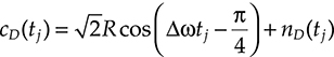
(9.41)
is obtained, where all the noise terms are collected into nD(tj) that results, with a very good approximation, a white Gaussian noise.
This function is now independent from the transmitted signal and it can be used to drive the frequency tracking circuit.
9.3.3.2 M-DPSK Optimum Receiver
Although the quadrature receiver can work with M-DPSK signals once a suitable decision rule is implemented, it is not the optimum receiver, which is the receiver assuring the minimum error probability in the presence of optical noise.
Moreover, the quadrature receiver is very complicated in architecture and requires high speed electronics, with all the consequences in terms of costs and power consumption.
Thus, it is also practically very important to design a simpler receiver for M-DPSK signals.
The receiver scheme is shown in Figure 9.32 and is the analogous of the binary DPSK receiver shown in Chapter 6, but for the fact that to better use the received power a balanced configuration has been adopted.
The idea is to use the signal as a sort of LO by delaying it of a symbol interval and leveraging on the differential encoding at the transmitter.
If the transmitted signal has the form (9.16), at the receiver the signal writes as
→E(t,k)=√Peiθ(k)ηT→∈+ηT→ηASE(t)(9.42)
![]()
(9.42)
where
k indicates the considered symbol interval
θ(k) depends on the symbol transmitted in the kth symbol interval
→∈![]() is the normalized field polarization vector
is the normalized field polarization vector
FIGURE 9.32 Block scheme of a balanced M-DPSK receiver. (From Yamazaki, H. et al., Photon. Technol. Lett., 22(5), 2010.)
the ASE noise contribution is represented with →ηASE(t)![]() (while it is to remember that ηT represents the function equal to one in the symbol interval and zero elsewhere)
(while it is to remember that ηT represents the function equal to one in the symbol interval and zero elsewhere)
The field on the upper branch of the receiver, after splitting, delay, and recombination, writes as
→E(t,k)=√Pα{eiθ(k)+eiθ(k−1)}ηT→∈+αηT→η′ASE(t)(9.43)

(9.43)
where α is the optical chain loss, and an analogous expression holds for the field in the lower branch and
→η′ASE(t)=ηASE(t)−→ηASE(t−Ts)(9.44)
![]()
(9.44)
Detecting the fields with a balanced receiver gives the following photocurrent
c(t)=RPα2cos(2πjM)ηT+2R√Pα2ηTRe{[eiθ(k)+e−iθ(k−1)]→η′ASE}+α2|→η′ASE(t)|2ηT+ns(t)(9.45)

(9.45)
where ns (t) is the shot noise term.
In equation (9.45) the symbol transmitted in the k-th symbol interval is represented by j, that determines the phase of the cosine function. The photocurrent is then sampled after low pass filtering and the samples are sent to the decision device.
The receiver we have described is much simpler than the whole quadrature receiver: no LO and no polarization tracking are needed due to the use of signal self-beating.
This is one of the reasons that qualify M-DPSK modulation as a good candidate for long haul 100 Gbit/s systems, where limiting the system cost is frequently much more important to push performances up to the limit.
9.3.3.3 M-PolSK Receivers
As in the case of M-DPSK, in the case of polarization modulation also, the quadrature receiver is not optimum and a direct detection receiver offering better performances can be designed [37,36].
The possibility to perform direct detection also contributes to simplify the receiver structure eliminating the need of the LO, but polarization tracking is needed since the transmitted information is coded in the polarization itself.
The idea on which optimum receivers, both coherent and direct detection, are designed is to detect the Stokes parameters to be able to operate processing and decision in the Stokes space.
The block scheme of the optimum M-PolSK receiver is presented in Figure 9.33, and it is composed of a front end producing four photocurrents that are proportional to the Stokes parameters and by an electronic processing section that is in charge to compensate polarization fluctuations, in the coherent case to drive the LO frequency locking and to perform symbol decision.
The block scheme of the coherent front end is reported in Figure 9.34; it is a combination of an heterodyne optical receiver and of square law type electronic demodulation that allows the Stokes parameters of the incoming field to be detected.

FIGURE 9.33 Functional scheme of the optimum M-PolSK receiver.

FIGURE 9.34 Coherent front end of a PolSK receiver; BS, Beam Splitters; PBS, Polarization Beam Splitters.
As far as Direct Detection is concerned, implementing an optical front end that is able to detect the Stokes parameters is equivalent to search the structure of a direct detection polarimeter. Several such polarimeters are used in practice, based on different principles, and the optical front end scheme of choice depends essentially on practical considerations.
An example of direct detection front end is reported in Figure 9.35: this structure is based on the analysis of the incoming field by means of quarter and half wave plates and polarization beam splitters. The input electrical field is divided by means of a polarization beam splitter into its linear polarization components and then these are combined by means of a couple of standard beam splitters of splitting ratio ε1, a couple of standard beam splitters of splitting ratio ε2, and a couple of polarization beam splitters as shown in the figure. If the optical path is accurately controlled, the two polarization components are combined in phase (technically means with the same phase) before detection on the second photodiode and in quadrature on the third one.
This structure is difficult to be realized via discrete components, due to the need of a very accurate control of the length of the light paths. On the other hand, it is quite suitable to be implemented by hybrid integration, where all the splitting structure shown in gray in the figure is integrated in a single silicon on silica chip. In this case, the phase control can be implemented by thermal phase controller and the structure results quite stable.
At the output of the interferometric polarimeter, the photocurrents results to be a linear combination of the Stokes parameters, thus inverting this relation, an estimate of the Stokes parameters is obtained.
Another interesting example of direct detection polarimeter is reported in [57] and it is based on the analysis of the incoming field by means of half and quarter wave plates. This structure does not require optical path length control and it is promising for discrete components implementation.
Finally, a polarimeter can be designed based on the fact that partially reflecting mirrors reflects the orthogonal linear polarization in different ways. Its schematic block diagram is shown in Figure 9.36.

FIGURE 9.35 Direct Detection front end of a PolSK receiver based on half and quarter wave plates: BS indicates unbalanced Beam Splitters; PBS, Polarization Beam Splitters; DL, Delay Line; A is the matrix relating the photocurrents to the Stokes parameters.
FIGURE 9.36 Direct Detection front end of a PolSK receiver based on partially reflective coating of four photodiodes.
Three photodetectors are coated with a reflection coating characterized by reflection parameters ψk, ρk, and κk (k = 1, 2, 3) while the fourth photodetector is antireflection coated so that all the optical power incident on it is detected. In particular, ρk indicates the reflectance of the surface for circular or unpolarized light, κk exp (i ψk) is the ratio between the complex reflection coefficient for linearly polarized light along parallel and perpendicular directions to the local incidence plane.
In all the cases we have considered up to now, a direct detection polarimeter produces four photocurrents that changes while the polarization of the received field changes. It is possible to demonstrate that in all the cases we have considered, there is a linear relation between the Stokes parameter and the currents at the output of the polarimeter that does not depend on the received polarization, thus it is possible to characterize the polarimeter with a matrix A so that, if the four currents at the polarimeter output are collected in a vector C, we can write [58,59]
(S1S2S3)=AC(9.46)

(9.46)
Since the current at the output of the electrical demodulation in the coherent receiver shown in Figure 9.34 is also proportional to the Stokes parameters and the proportionality is a particular type of linear dependence, we will assume Equation 9.46 as valid for any type of optical front end in an M-PolSK receiver.
As far as the electrical processing section is concerned, it is in charge to perform both fiber polarization tracking and, in the coherent case, of generating the driving signal for the frequency lock of the LO.
Different algorithms have been proposed for these functions and we will not review them in detail.
Some algorithms use the same ideas we explained dealing with the quadrature receiver. In this case, the modulation is eliminated by using a decision driven algorithm that inverts the modulator operation starting from the estimate of the transmitted symbol [35].
Other algorithms use the idea that the constellation can be designed so that the average value of the Stokes vector over the entire constellation is not the null vector.
In this case, the modulation can be eliminated by simply averaging the modulated field over a time long with respect to the symbol time: the result is an average field whose polarization fluctuations are only due to the fiber propagation.
In this case, simply observing the variations of such an average vector, the fiber-induced polarization rotations can be compensated [35].
The last class of algorithms has the very important advantage not to require electronics speed comparable to the symbol rate, but it is not applicable to all the constellations, requiring an average Stokes vector different from zero.
9.3.4 Ideal Performances of Multilevel Systems
In this paragraph, we will compare different multilevel modulation formats considering only the limitation deriving from ASE. This approach is justified by the fact that in optically amplified systems, generally an optical preamplifier is placed in front of the receiver, so that the received power is sufficiently high to neglect both receiver thermal noise and shot noise.
Naturally, in real systems, several other elements thwart the system performances; however, a first approach based only on noise consideration is quite useful to have a first comparison among different systems.
As in the case of binary systems, also the performances of multilevel systems are evaluated considering the bit error probability. As a matter of fact, in real applications, the original message is almost always binary and multilevel coding is used only to ease the transmission.
Let us assume, as usual, that errors are independent from the transmitted symbol and from the pattern transmitted in the previous symbol intervals. The bit error probability Pe and the symbol error probability PS are related by the equation
Pe=〈e〉log2MPs(9.47)

(9.47)
The average number of wrong bits <e> consequent to a symbol error depends on the coding, that is, on the association between bit patterns and points in the multilevel constellation. This association is generally called tagging of the constellation.
In order to have the minimum error probability, it is useful to tag a constellation in such a way that nearby points corresponds to nearby bit words. In the case of squared constellations, tagging is easy due to the fact that the constellation can be divided into the Cartesian product of one dimensional constellations.
If the number of one dimensional constellations is n (e.g., two for M-QAM, or four for M-4QAM), also the bit word has to be divided into n parts and each part is the tag of one one dimensional constellation.
This tagging technique is shown in Figure 9.37 in the case of 16-QAM. In the case of more complex configurations, tagging can be much more complicated, and it is also possible that in a few cases the adjacency of symbols corresponding to very different bit words cannot be avoided.
An upper bound for the number of erroneous bits in a wrong symbol can be obtained assuming that, when a symbol is wrong, the receiver produces a random symbol among the M − 1 different from the transmitted one.
In this case, if n = log2M,
〈e〉=1M−1nΣk=1(nk)=1M−1n−1Σk=0n(n−1)!k!(n−1−k)!=Mlog2M2(M−1)(9.48)

(9.48)
FIGURE 9.37 Tagging of a squared constellation.
where besides the definition of n the following combinatorial property has been used:
rΣk=0(rk)=2r(9.49)

(9.49)
Thus, the following upper bound can be used for the error probability, if the symbol error probability is known:
Pe=M2(M−1)Ps(9.50)

(9.50)
As far as the symbol error probability is concerned, it depends on the decision criterion adopted to produce an estimate of the transmitted symbol.
We will consider here only the so-called “hard decision” criteria, where the estimate of the transmitted symbol is produced by the decision device without taking into account the presence of a FEC. After hard decision, the produced symbol stream (or often the produced bit stream after multilevel decoding) is passed to the FEC for error correction [43,60].
Traditionally, soft decision criteria, where decision and FEC decoding are not divided, but the decision device uses the FEC redundancy also to take the better possible estimate of the transmitted message, has been considered too complex to be used at optical transmission speed. This situation is changing with the increase of the speed of C-MOS electronics and it is possible that soft decision decoders will also become available at optical speeds quite soon [60].
Due to the better exploitation of the information contained in the received message, generally, soft decision performs better than hard decision, with a gain of the order of a couple of dBs at the typical optical SNo level.
A hard decision-based decision device for a multilevel modulation format is based on the division of the space in which the multilevel constellation is created (e.g., the quadrature space or the Stokes space) in decision zones, let us call them Oj with j = 1, 2, …, M, each of which contains only one constellation point.
The decision device simply associates the received signal to the constellation point inside the same decision zone. Naturally, to achieve good performances, the decision zones have to be optimized in order to minimize the overall error probability.
Assuming that the noise distribution is isotropic around any constellation point, the optimum decision zones coincides with the so-called Voronoi zones of the multilevel constellation and they can be individuated with the so-called elementary cell method [46,61].
The method works as follows. In order to determine the Voronoi zone of the jth point of the constellation, as a first step the considered point is connected with M − 1 oriented segments with all the other constellation points. Let us call Πj the jth point and ¯ΠjΠk![]() the segment connecting the jth point with the kth point.
the segment connecting the jth point with the kth point.
From now on, as in the notation ¯ΠjΠk![]() , we will indicate with upper-line capital letters like ¯AB
, we will indicate with upper-line capital letters like ¯AB![]() vectors in an abstract space individuated by the end points (A and B in the example), coherently with the notation that we have adopted, where ˉX
vectors in an abstract space individuated by the end points (A and B in the example), coherently with the notation that we have adopted, where ˉX![]() indicates a vector in an abstract space, while →E
indicates a vector in an abstract space, while →E![]() a physical vector (for example the electrical field).
a physical vector (for example the electrical field).
Calling ˉZ![]() the vector representing the received field, let us construct the projections of ˉZ
the vector representing the received field, let us construct the projections of ˉZ![]() over ¯ΠjΠk
over ¯ΠjΠk![]() and call it zj,k. It is a random variable, due to the presence of the noise, and it can be defined as the following probability
and call it zj,k. It is a random variable, due to the presence of the noise, and it can be defined as the following probability
P(Zj,k>Cj,k/Πj)=∞∫Cj,kp(zj,k/Πj)dσj,k(9.51)

(9.51)
where
cj,k is a threshold fixed on ¯ΠjΠk![]()
zj,k is the curve coordinate along ¯ΠjΠk![]()
p (zj,k/Πj) is the probability density function of the projection zj,k
Let us optimize the threshold cj,k to minimize the probability P (j,k) that is given by
P(j,k)=∞∫cj,kp(zj,k/Πj)dσj,k+∞∫cj,kp(zk,j/Πk)dσj,k(9.52)

(9.52)
Once optimized the threshold, let us consider, for any k = 1, 2, …, M and different from j, the plane orthogonal to the segment ¯ΠjΠk![]() and passing by cj,k. In this way, M − 1 planes are individuated. The optimum decision zone is the minimum volume individuated by such planes.
and passing by cj,k. In this way, M − 1 planes are individuated. The optimum decision zone is the minimum volume individuated by such planes.
As an example, the optimum decision zones for 4-QAM are the four quadrature plane quadrants, shown in Figure 9.38.
Once the decision zones have been optimized, the decision procedure leads to the following equation for the symbol error probability:
Ps=1MMΣK=1 ∫Uj≠kDjp(ˉZ/ˉCk)dˉZ(9.53)

(9.53)
where
ˉZ![]() indicates the points representing in the constellation space the received field
indicates the points representing in the constellation space the received field
ˉCk![]() indicates the constellation kth point
indicates the constellation kth point
p(ˉZ/ˉCk)![]() is the probability density function that ˉZ
is the probability density function that ˉZ![]() is received when ˉCk
is received when ˉCk![]() is transmitted Integral in dˉZ
is transmitted Integral in dˉZ![]() is a volume integral into the constellation space
is a volume integral into the constellation space

FIGURE 9.38 Hard decision for 4-QAM.
Several techniques have been devised to manage integrals like that in Equation 9.53, comprising an n-dimensional extension of the Saddle point approximation [61]. However, since we will deal in any case with low symbol error probabilities, the easier way to go is to evaluate the integral (9.53) using the so-called union bound.
The union bound is an asymptotically exact approximation of an integral in the form (9.53) that exploits the definition of the optimum decision zones to approximate the integral as follows
Ps=1MMΣk=1 ∫Uj≠kDj p(ˉZ/ˉCk)dˉZ≈1MMΣk=1 MΣj=1j≠1 ∞∫Cj,kp(zj,k/Πj)dσj,k(9.54)

(9.54)
Equation 9.54 shows as the union bound reduces the decision process to a set of binary decisions along the direction connecting the points of the constellation.
Generally, the noise distribution has an exponential tail, thus the main contribution to the error probability is given by the first neighbors of the considered point. If it is possible to limit the evaluation only to this contribution, Equation 9.54 further simplifies yielding
Ps=1MMΣk=1 ∫Uj≠kDj p(ˉZ/ˉCk)dˉZ≈1MMΣk=1 γk∞∫Ckp(zk/Πj)dσk(9.55)

(9.55)
where
γk is the number of first neighbors
zk is the projection of the received vector along the direction connecting the considered point with one of the first neighbors
σk is the curve coordinate along this direction
Finally, if the constellation is a regular lattice, where all the points have the same number of first neighbors located at a fixed distance and if the noise has the same distribution whatever symbol is transmitted (situation very common for regular lattices), a further simplification of (9.55) is possible since the optimum threshold, for symmetry reasons, is located at half the distance between first neighbors.
Thus in this case it is possible to write
PS=γ∞∫d/zp(z/Π)dσ(9.56)

(9.56)
where d is the distance between first neighbors and the other symbol has the same meaning as in (9.56) with useless indices eliminated.
In the remaining of this paragraph we will use the above equations to analyze the ideal performances of 100 Gbit/s amplified multilevel systems using different types of modulation and detection.
The general system scheme used for this evaluation is reported in Figure 9.39, which is similar to Figure 6.18, but for the presence of multilevel modulation. We will assume the spans to be of the same length and, due to the presence of the preamplifier, we will neglect shot and thermal noise.
As seen in Chapter 6, the ASE noise spectral distribution is given by
SASE={αLSIn(Gil)(Gil−1)NFil+(Gp−1)NFp+(Gb−1)NFb}ħω(9.57)

(9.57)
where
Ls is the span length
Gil is the in-line amplifier gain
Gb is the booster amplifier gain
Gp is the preamplifier gain
NFil is the in-line amplifier noise factor
NFb is the booster amplifier noise factor
NFp is the preamplifier noise factor
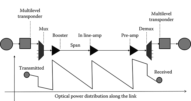
FIGURE 9.39 Architecture of the amplified system used to evaluate theoretical performances of the considered modulation formats at 100 Gbit/s.
We will not follow in detail all the calculations that are needed to arrive at the error probability for each format/receiver. The methods are all explained in Chapter 6 so that for the interested reader it should not be difficult to reconstruct the steps to arrive to the results.
9.3.4.1 M-QAM and M-4QAM with Quadrature Receiver
First we will analyze the coherent quadrature homodyne receiver.
In this case, as evident from Equation 9.35, the dominant noise term is the ASE component of the photocurrent that results amplified by the local oscillator.
This term is linear in the ASE amplitude, thus resulting in a Gaussian white noise at the electrical level. Since attenuations due to the receiver are experienced both by the signal and by the ASE noise, these do not appear in the error probability, at least as far as the ASE term is the dominant noise.
Thus, the electrical signal to noise ratio SNE is given by
SNE=PSASERS(9.58)

(9.58)
where the baseband has been assumed equal to the symbol rate. Using the approximation (9.56) with γ equal to the average number of first neighbors for the symbol rate and the bound (9.50),
Pe=γM2(M−1)Q(d√SNE2)(9.59)
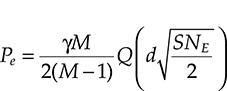
(9.59)
is obtained where d is the normalized minimum distance of the constellation. From Equation 9.59 the importance of maximizing the constellation minimum distance is clearly seen.
In Figure 9.40, the error probability is plotted for a multilevel M-QAM system using a quadrature receiver. Due to the rapid decrease of the minimum distance with the number of constellation points, the performances get rapidly worse increasing the number of levels. On the other hand, for a low number of levels, this is an effective modulation format.
FIGURE 9.40 Plot of the ideal performance of M-QAM for various values of the number of levels.
Better performances at high number of levels are attained by the constant power M-4QAM, whose constellations are derived from regular convex solids in the four dimensional space.
In Figure 9.41, the error probability for this kind of modulation is shown, deriving the constellation with 64 points from a random selection of points among the vertices of the 600 Tetrahedral (120 vertices) and the constellation with 512 points from a random selection of 512 among the 600 vertices of the 120 Dodecahedral. No attempt has been made to optimize the choice, although there is a large literature about segmenting of complex constellations and the interested reader is encouraged to start from [62–64] if is interested in methods for an optimum subconstellation selection.
Increasing the number of levels, the performance is far better with respect to M-QAM, due to the better exploitation of the available degrees of freedom.
Finally, in Figure 9.42, variable power M-4QAM performances are represented in the case of the constellations of Table 9.5. The high number of degrees of freedom renders these modulation formats extremely efficient at very high number of levels, even if at low number of levels the performances are not superior to that of other quadrature based formats.
FIGURE 9.41 Plot of the ideal performance of constant power M-4QAM for various values of the number of levels

FIGURE 9.42 Plot of the ideal performance of variable power M-4QAM for various values of the number of levels in the case of the constellations of Table 9.5
9.3.4.2 M-PolSK with Stokes Parameters Receiver
Following the receiver structure to determine the expression of the decision variable and its statistics, it is possible to demonstrate the following properties:
The decision variable is a quadratic form of the input field quadratures
The decision variable is independent from the polarimeter matrix A if the ASE noise is dominant
The decision variable statistic is independent from the fiber polarization rotation; this property derives from the fact that the ASE power is uniformly distributed on the Poincarè sphere among all the polarization states
The last two properties, which are a key to evaluate the performance of various PolSK systems, deserve a comment.
Let us consider the evolution of the M-PolSK signal under the polarization point of view representing it in the Stokes space. Let us indicate with ˉS![]() the Stokes vector having for components the three Stokes parameters that are coordinates in the Stokes space.
the Stokes vector having for components the three Stokes parameters that are coordinates in the Stokes space.
If the Launched signal is represented with ˉSi![]() , after fiber propagation, the Stokes vector ˉSo
, after fiber propagation, the Stokes vector ˉSo![]() in front of the receiver can be written as
in front of the receiver can be written as
¯So=M¯Si+ˉn(9.60)
![]()
(9.60)
where
M is the Muller matrix (the Stokes space version of the Jones matrix)
ˉn![]() is the ASE noise vector in the Stokes space
is the ASE noise vector in the Stokes space
Both coherent and direct detection receivers have an optical front end constituted by a polarimeter generating a photocurrents vector ¯C0![]() whose elements are proportional to the Stokes parameters. This means that a nonsingular matrix A can be found so that, neglecting distortions and the photodiode sensitivity,
whose elements are proportional to the Stokes parameters. This means that a nonsingular matrix A can be found so that, neglecting distortions and the photodiode sensitivity,
¯C0=A¯So(9.61)
![]()
(9.61)
The polarimeter is followed by an electronic processing section that has the role of inverting the matrix to obtain a set of photocurrent ¯C1![]() proportional to the received field Stokes parameters.
proportional to the received field Stokes parameters.
This means that, whatever be the polarimeter, coherent or incoherent, the currents in front of the electronic polarization compensation section have the following expression:
¯C1=A−1ˉC0=¯So(9.62)
![]()
(9.62)
Remembering that ˉSo![]() does not depend on the receiver structure, we can conclude that the decision variable is exactly the same in every ideal Stokes parameters receiver and thus all these receivers have the same performances.
does not depend on the receiver structure, we can conclude that the decision variable is exactly the same in every ideal Stokes parameters receiver and thus all these receivers have the same performances.
At this point, it is useful to choose the receiver structure that makes easiest the evaluation of the BER, and it is for sure the coherent receiver.
Due to the square law detection operated at the electrical level, the decision variable is still a quadratic form of the field quadratures.
In these conditions, the saddle point approximation (see Chapter 6) can be used to evaluate the error probability if the union bound is used. As a matter of fact, this approximation allows us to decompose the decision process in a set of independent binary decisions.
Moreover, among all the addenda entering in the union bound expression of the symbol error probability we can maintain only those relative to first neighbors.
The characteristic function of the decision variable relative to the decision on the segment among a couple of first neighbors is given by
Fc(s)=exp[−SNo(d2Moes/4)((1−4s2)/(1−d2s2))](1−d2s2)2Moe(9.63)

(9.63)
where
Moe is the ratio between the optical and the electrical bandwidth
SNo is the optical signal to noise ratio
d is the distance between first neighbors in the Stokes space
A simple closed form expression of the bit error probability it is not easy to achieve, due to the complexity of the calculation involved by the saddle point approximation.
Since a simple formula is important for quick evaluation, we have derived an approximated form of the error probability assuming a high signal to noise ratio and the condition SNo≫M2oe![]() that is always realized in practice.
that is always realized in practice.
Moreover, we have decided to put Moe = 2, so that the electrical and the optical SN coincides (the difference is smaller than 2%).
Expressing the error probability as a function of SNe allows us to consider the dependence of the BER on Moe as slow and, for 0.5 < Moe < 4 negligible in a first approximation (see Chapter 6).
Under these hypotheses, the bound optimization parameters s0 can be approximated with a simple expression
s0(SNe,d)=(1SNe)(a2d2+a1d+a0)+(b5d5+b4d4+b3d3+b2d2+b1d+b0)(9.64)

(9.64)
where the numerical value of the approximation parameters are reported in Table 9.7. The ratio between the approximation standard deviation and the average is smaller than 0.6% in all the parameter domain suitable for the applications.
Table 9.7 Values of the Approximation Parameters That Are Present in the Expression of the Error Probability of Direct Detection M-PolSK
b5 |
−35.241 |
||
b4 |
15.202 |
||
b3 |
−26.489 |
||
b2 |
23.732 |
a2 |
−0.1117 |
b1 |
−11.320 |
a1 |
0.4341 |
b0 |
2.809 |
a0 |
0.7513 |
Once s0(SNe, d) is evaluated, in the approximation of high SN the optimum threshold is always 0.5 SNe and the saddle point approximation can be further simplified yielding
Pe=γM2(M−1)e−SNes0[(4−d2)/2(d2s20−1)+23/10](1−s20d2)4(9.65)

(9.65)
The accuracy of the approximation can be verified comparing the results with the exact saddle point expression evaluated by numerical solution of the bound parameter equation and of the resulting expression of the error probability reported in [37]. The error is never above 0.3 dB as far as the error probability is lower than 10−3 in all the cases reported in [37].
The performances of coherent detection M-PolSK are shown in Figure 9.43 using the configurations whose parameters are reported in Table 9.3, the 32 level system constellation is derived by randomly selected 32 points out of the 60 vertices of the snub-dodecahedron and the 64 points constellation by randomly selecting 64 out of the 120 vertices of the Icosidodecahedron. In the figure, the performances of a coherent detection M-PolSK system using the optimum constellations reported in [35,37] are also plotted in dashed lines. It is evident that the sensitivity gain related to the use of the optimum constellation with respect to a more regular suboptimum one is small and probably in practice it is cancelled by the difficulty to reproduce accurately the optimum configurations due to their more complex structure.
9.3.4.3 M-DPSK with Direct Detection Receiver
Last of the modulation formats we have considered is multilevel DPSK with direct detection receiver.
Due to its structure based on signal self beating, the receiver belongs to the class of quadratic receivers. In this case, the problem of determining the symbol error probability from the characteristic function can be exactly solved as already underlined in Chapter 6 for the binary case. Passing from the symbol error probability to the bit error probability, we obtained
Pe=M2(M−1)e−SNed2/2(9.66)
![]()
(9.66)

FIGURE 9.43 Plot of the ideal performance of PolSK with Stokes Parameters Receiver and for various values of the number of levels and Moe = 2. Results obtained with optimum constellations reported in [35,37] are plotted too in dashed lines.

FIGURE 9.44 Ideal performances of M-DPSK for different values of the number of levels M.
Equation 9.65 is used to evaluate the performance of an M-DPSK system that are shown in Figure 9.44. As expected, this modulation format gets rapidly worse by increasing the number of levels, due to the fact that it is based on the modulation of a single degree of freedom. For a low number of levels, however, the penalty with respect to other formats is smaller and in practice, especially at very high speed as 100 Gbit/s, it could be more than counterbalanced by the simplicity of the receiver with respect, for example, to the quadrature receiver.
9.3.4.4 Comparison among Different Modulation Formats
In Figure 9.45, the sensitivity of the various systems we have analyzed are represented for a BER of 10−4, typical of applications with FEC. Collecting the results, they can be divided into two sets, with different and well individuated behaviors with respect to the number of levels.
This is essentially due to the fact that the BER trend with the number of levels is essentially a metric property of the constellation, thus depending on the characteristics of the space to which the constellation belongs.

FIGURE 9.45 Sensitivity of different multilevel modulation formats in ASE-limited conditions at BER = 10−4.
In order to have better trends, it seems that either the number of degrees of freedom has to be increased, or the space metrics has to be changed (passing, e.g., from a plane to a sphere), the first step being more effective than the second.
9.3.5 Coherent Receivers Sensitivity to Phase and Polarization Fluctuations
At the end of this section devoted mainly to the performances of multilevel transmission systems, it is necessary to consider an important element regarding coherent detection that comes into play any time the transmission system cannot be considered ideal.
We will take as a reference the receiver presented in Section 9.3.3.1, that is, the universal quadrature receiver, but what we will present in this section can be adapted at almost any coherent receiver with marginal modifications to take into account the receiver structure.
The main advantage of coherent detection is that the set of electrical currents at the output of the receiver are proportional to the field quadratures, but for the noise. This property allows information to be coded into any degree of freedom of the optical field thus fully exploiting its transmission potential.
On the other hand, this also means that any form of random fluctuation of the field is detected by the receiver and constrains its performances.
Here we will consider the two main noises that can limit the performance of a coherent receiver while in a direct detection receiver these noises can be generally neglected: the phase noise and the polarization noise.
9.3.5.1 Phase Noise Penalty for Coherent Quadrature Receiver
Several causes can generate phase noise on the optical signal before detection: generally, the most important are the frequency fluctuations of the transmitting laser and of the LO and the nonlinear phase noise coming during propagation from Kerr effect. We will consider here the phase noise derived from the frequency fluctuations of the lasers.
The phase noise has a complex degrading effect: it reduces the power available for symbol estimation on each quadrature, introduces a rotation of the (e1, e2) and (e3, e4) planes in the quadrature space creating crosstalk between the corresponding quadratures, and finally it creates imperfect frequency lock between the LO and the received field carrier.
As a matter of fact, Equation 9.34 is rewritten in this case as
c1(tj)=R[e1(tj)+η1(tj)]cos(φT−φL)+R[e2(tj)+η2(tj)]sin(φT−φL)+n1(tj)c2(tj)=R[e2(tj)+η2(tj)]cos(φT−φL)−R[e1(tj)+η1(tj)]sin(φT−φL)+n2(tj)c3(tj)=R[e3(tj)+η3(tj)]cos(φT−φL)+R[e4(tj)+η4(tj)]sin(φT−φL)+n3(tj)c4(tj)=R[e4(tj)+η4(tj)]cos(φT−φL)−R[e3(tj)+η3(tj)]sin(φT−φL)+n4(tj)(9.67)

(9.67)
where
φT represents the transmitter phase noise
φL is the phase noise of the LO
The problem of an accurate evaluation of the impact of phase noise on this class of receivers has been studied extensively; several models have been devised with different levels of accuracy and complexity for all the relevant modulation formats. It is not our intention here to either develop an accurate model or to compare different models in different situations; the interested reader is encouraged to personally analyze the rich technical literature starting from the literature reported in [31].
In practical high performance systems, very high quality tunable lasers are used to reduce cost of spare parts, to ease the LO operation, and to minimize the effect of phase noise via a very narrow linewidth. In general, the linewidth is smaller than a few MHz and in the external cavity, the linewidth is of the order of 500 kHz.
In this condition, we have to expect that in general the phase noise impact will be small, which is a necessary condition for our draft design. Thus we will introduce a very simplified model for the analysis of the phase noise impact, which holds in the low penalty regime. This model will allow us to evidence all the elements that are important and also to obtain a closed form expression of the sensitivity penalty.
In the low penalty condition, Equation 9.67 can be linearized with respect to the phase noise obtaining
c1(tj)=R[e1(tj)+η1(tj)]+R[e2(tj)+η2(tj)](φT−φL)+n1(tj)c2(tj)=R[e2(tj)+η2(tj)]−R[e1(tj)+η1(tj)](φT−φL)+n2(tj)c3(tj)=R[e3(tj)+η3(tj)]+R[e4(tj)+η4(tj)](φT−φL)+n3(tj)c4(tj)=R[e4(tj)+η4(tj)]−R[e3(tj)+η3(tj)](φT−φL)+n4(tj)(9.68)

(9.68)
From (9.68), it is clear that the phase noise presence in the regime of small ratio between the linewidth and the symbol rate has a first effect of creating an additional noise composed of two terms: one proportional to the signal power and the other to the ASE.
The noise term proportional to the signal power is particularly dangerous, since its effect cannot be compensated by increasing the transmitted power.
As far as the effect on the frequency lock is concerned, Equation 9.41 is substituted in the presence of phase noise with
cD(tj)=√2Rcos[Δωtj−π4+φT(tj)−φL(tj)]+nD(tj)(9.69)
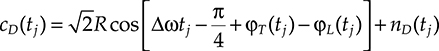
(9.69)
so that, assuming an ideal frequency lock, a simple first order digital filter to limit the lock loop bandwidth and neglecting in conditions of low penalty the unlock probability, the estimated frequency deviation Δωe can be expressed as
Δωe=Δω+δω=Δω+1N1N1Σj=1φT(tj)−φL(tj)−φT(tj−1)+φL(tj−1)Δt(9.70)

(9.70)
where
Δt is the sampling rate
NI is the lock loop bandwidth in terms of number of integrated samples so that the loop bandwidth is BI = 1/NIΔt
This error in the estimated angular frequency causes a further element to be added to the photocurrent. In small phase noise regime, Equation 9.69 becomes
c1(tj)=R[e1(tj)+η1(tj)]+R[e2(tj)+η2(tj)](φT−φL+δωtj)+n1(tj)c2(tj)=R[e2(tj)+η2(tj)]−R[e1(tj)+η1(tj)](φT−φL+δωtj)+n2(tj)c3(tj)=R[e3(tj)+η3(tj)]−R[e4(tj)+η4(tj)](φT−φL+δωtj)+n3(tj)c4(tj)=R[e4(tj)+η4(tj)]−R[e3(tj)+η3(tj)](φT−φL+δωtj)+n4(tj)(9.71)

(9.71)
Since we have assumed to use a small linewidth laser, we can assume that its linewidth is Lorentian with a very good approximation.
For a laser with a Lorentian linewidth Δν, the following equation holds [31]:
Δv=12πSφ(0)(9.72)
![]()
(9.72)
where S.φ(0)![]() is the frequency noise spectrum evaluated for zero frequency (see Chapter 5).
is the frequency noise spectrum evaluated for zero frequency (see Chapter 5).
Moreover, the following relation exists between the phase noise variance and the frequency noise spectrum:
σ2φ=2π∞∫0S˙φ(ω)1−cos(ωTS)ω2dω≈2πS˙φ(0)2πBφ∫01−cos(ωTS)ω2dω=TSπ2S˙φ(0)F(TSBφ)(9.73)

(9.73)
where TS is the symbol interval, Bφ is the laser S˙φ(ω)![]() spectral width (of the order of 2–3 GHz; see Chapter 5) and
spectral width (of the order of 2–3 GHz; see Chapter 5) and
F(x)=x∫01−cos(2πν)ν2dν(9.74)

(9.74)
Assuming that both transmitter and LO have the same linewidth, the variance of the phase fluctuations in a bit interval can be expressed as a function of the laser linewidth as follows:
σ2φ=2πΔvRsF(BφRs)(9.75)

(9.75)
As far as the angular frequency lock error is concerned it is a Gaussian zero mean process. Its variance can be calculated easily taking into account that the summation can be simplified so that only the terms in the first and the last instants of the interval remain.
σ2δω=4πΔvRSB2IF(BφRS)(9.76)

(9.76)
where
BI is the lock loop bandwidth
It derives a general result: better performances of the LO lock loop are achieved if it is possible to find a loop bandwidth sufficiently large to efficiently follow the lasers parameters fluctuations but much smaller than the symbol rate.
In the low penalty limit, we will assume that the error probability expression versus the SNe does not change, thus the penalty can be evaluated evaluating the SNe.
We can always rotate the reference system in the quadrature space so that the e1 axis is along the segment joining the two first neighbors we are considering. In this way, it is e2 = e4 = e3 = 0 and the decision variable C, at the first order in the phase noise, has the following form:
C=4Σj=1c1(td)=R[e1(tj)+η1(tj)]−R[e1(tj)+η1(tj)](φT−φL+δωtd)+4Σj=1nj1(td)(9.77)

(9.77)
To evaluate the electrical SNe we will neglect the additive noise with respect to the ASE contribution and all the terms of second order in the noise.
Moreover we note that
〈(φT−φL+δωtd)2〉=4πΔvRSF(BφRS)[1+BIRS+(BIRS)2](9.78)

(9.78)
due to the fact that δω and φT – φL are not uncorrelated and their product cannot be set to zero.
Finally
SNe=Pd2SASERS+(4/π)Pd2(Δv/RS)F(Bφ/RS)[1+(BI/RS)+(BI/RS)2](9.79)

(9.79)
The behavior of the SNe in the presence of Phase noise for M-4QAM is plotted in Figure 9.46.

FIGURE 9.46 SNe penalty due to phase noise for M-4QAM in the approximation of small impairment.
The most striking feature of the curves representing the SNe behavior is the presence of a clear plateau due to phase noise. When the plateau is reached, increasing the power does not change the SNe due to the fact that the phase noise term also depends on the power.
9.3.5.2 Depolarization Penalty for Coherent Quadrature Receiver
The working of the coherent quadrature system is based on the assumption that the evolution of the signal polarization is linear so that a linear estimate of the channel can completely compensate the polarization rotation.
If a nonlinear polarization evolution is stimulated by the high transmitted power, this is no more true and a further sensitivity penalty is induced by this phenomenon.
In a first approximation, we can divide polarization fluctuations between fast nonlinear and slow linear. Due to the fact that the linear polarization tracker has a small bandwidth, it passes through the fast part of polarization fluctuations.
Kerr-induced polarization fluctuations, depending on the transmitted message, can be seen as a random process inducing random time depolarization of the received field [65].
As far as the induced depolarization degree is small, we can imagine that it is passed through by the polarization tracker so that practically only the linear fluctuations are tracked and the nonlinear depolarized field appears to fluctuate randomly after multiplication by the inverse of the Jones matrix and have to be dealt as signal dependent noise.
Calling δPOL the nonlinear depolarization degree, which is the reciprocal of the polarization degree defined in Equation 9.34, the received optical field can be written as
→E(t)=E(t)[√1+δPOL(aeiΨ→p++√1−a2→p−)+√δPOL→ζ(t)](9.80)
![]()
(9.80)
where
ˉζ(t)![]() (t) is a randomly varying unitary vector determined by nonlinear polarization evolution that has a bandwidth larger than RS
(t) is a randomly varying unitary vector determined by nonlinear polarization evolution that has a bandwidth larger than RS
a and ψ are the Jones matrix parameters (along with an absolute phase here set to zero) that the polarization tracker has to estimate
Even if the correlation between the depolarized and the polarized part of the field is not zero, a simple way to evaluate the impact of nonlinear polarization evolution is to consider the depolarized terms if it was a noise with a colored spectrum.
In particular, the expressions of the photocurrents after polarization recovery becomes
c1(tj)=R√1−δPOL[e1(tj)+η1(tj)]+√δPOL4Σh=1A1h[eh(tj)+ηh(tj)]+n1(tj)c2(tj)=R√1−δPOL[e2(tj)+η2(tj)]+√δPOL4Σh=1A2h[eh(tj)+ηh(tj)]+n2(tj)c3(tj)=R√1−δPOL[e3(tj)+η3(tj)]+√δPOL4Σh=1A3h[eh(tj)+ηh(tj)]+n3(tj)c4(tj)=R√1−δPOL[e4(tj)+η4(tj)]+√δPOL4Σh=1A4h[eh(tj)+ηh(tj)]+n4(tj)(9.81)

(9.81)

FIGURE 9.47 SNe penalty due to depolarization in the approximation of small impairment for M-4QAM.
The 4 × 4 matrix A is defined stating from the quadratures of M+ˉζ(t)![]() .
.
Due to its definition, A is a unitary matrix like M and it can also be interpreted as the random rotation induced by the combination between linear and nonlinear effects.
The expression of the photocurrent is formally similar to that derived for the case of phase noise, thus following the same derivation and assuming perfect linear polarization tracking yields
SNe=Pd2(1−δPOL)SASERS+Pd2δPOL=SNeo(1−δPOL)1+SNeoδPOL(9.82)
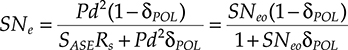
(9.82)
where SNeo is the ideal value of SNe in the same circumstances. The effect of depolarization is very strong, as shown in Figure 9.47, introducing a plateau in the SNe.
9.4 Alternative and Complementary Transmission Techniques
We have seen that multilevel modulation formats constitutes a very promising transmission technique to design long distance very high capacity optical links.
Besides multilevel modulation, there are a set of transmission techniques that can further improve the system performances, either helping to decrease multilevel sensibility to some transmission impairment or providing the way for a further ideal performance improvement.
The most important of these techniques is Orthogonal Frequency Division Multiplexing (OFDM), a technique for low speed channels multiplexing that simultaneously greatly reduce the sensitivity to linear causes of ISI and increase sensibly the bandwidth efficiency exploitation.
Besides OFDM, PDM and polarization diversity are often used to exploit the polarized nature of the electromagnetic field without an explicit polarization modulation and to decrease the sensitivity of the system to channel interference, respectively.
Also pulse polarization diversity is sometimes used, especially in RZ systems, to prevent the jitter caused by interaction between nearby pulses.
In this section, we will briefly introduce all these techniques.
9.4.1 Orthogonal Frequency Division Multiplexing
OFDM is used extensively in broadband and radio communication because it is an effective solution to ISI caused by a dispersion during signal propagation [66].
This becomes increasingly important as data rates increase to the point that the memory of the channel is not limited to a string of three bits, but extends to longer bit series. In this case, equalization is a complex matter requiring elaborated algorithms like mean-squared error (MSE) or signal back-propagation.
In contrast, the complexity of OFDM, using serial modulation and frequency domain equalization, scale well as data rates and dispersion increase.
The basic concept of OFDM is simple: data are transmitted in parallel on a number of different frequencies. Due to the parallelization of the data flux, the symbol period is much longer than that of a serial system with the same total data rate.
Due to the longer symbol period, the channel memory gets shorter, or even disappears completely, since dispersion only affects one symbol. In most OFDM implementations, any residual ISI is removed by using a form of guard interval between adjacent bit intervals called a cyclic prefix.
It could seem that this is simply frequency multiplexing, similar to what happens in WDM systems, but there are key differences between standard WDM and OFDM.
In standard WDM, the signals transmitted on different wavelengths are completely uncorrelated and guard intervals are used in between adjacent channels in order to reduce crosstalk. WDM multiplexing is performed using an analog optical device, and the same for demultiplexing.
OFDM on the other hand, is based on the digital generation of the multiplexed signal by densely packing channels that are generated to be orthogonal from a mathematical point of view.
Since the channels can be separated using their orthogonality, there is no need of guard intervals among them.
The generation of the multiplexed signal and the demultiplexing is operated via Fast Fourier Transform (FFT) by a dedicated processor; thus it is a computationally efficient and fast operation that can incorporate, if needed, equalization in the frequency domain.
It is not our scope to review in detail OFDM techniques, but it is quite clear that OFDM could become a useful technique to design very high speed long haul optical systems [67,69].
Naturally, OFDM also presents critical aspects, which have to be faced to design effective systems.
Among the technical criticalities of OFDM, there are the sensitivity to phase noise [69] and to unbalance between the quadratures at the receiver, for example, caused by differences between receiver hybrids [66].
As a matter of fact, it is easy to imagine that if the different carriers of an OFDM signal are constructed selecting amplitude and phase so that nearby carriers results to be orthogonal, any phenomenon introducing an uncontrolled phase element can alter this balance causing strong interference between nearby channels at the receiver, when they are demultiplexed in the frequency domain.
Since SPM introduces a nonlinear form of phase noise, the SPM sensitivity is another critical aspect of OFDM modulation.
The fact that the OFDM system has to be designed with a great care for the linearity both of transmitter and receiver and of fiber propagation is also due to the characteristics of the OFDM signal to have a great ratio between peaks and average value of the amplitude. These big fluctuations immediately create distortion if nonlinearity is encountered [70].
Distortion of this kind can be classified as Out Of Band Power and In Band Distortion. Out of band power not only creates a power penalty due to the loss of a part of the available power, but also could provoke interference if this power is reflected again in the signal bandwidth during the nonlinear propagation through the system [66].
Band distortion creates interference between the carriers.
Another potential critic aspect of OFDM is the cost of the transmitter and the receiver compared with a traditional transmitter or receiver of an IM-DD system.
However, this element tends to disappear more and more while traditional WDM systems are forced to use complex maximum likelihood sequence estimation (MLSE) or back propagation systems to compensate for ISI. As a matter of fact, these complex electronic equalization methods rely on high speed electronics, frequently on specific ASICS, so that the cost of OFDM is no more so high with respect to this kind of advanced IM-DD systems.
Since orthogonality among nearby channels is assured by the carrier, any modulation format can be used in principle on the subcarriers of an OFDM signal. Since OFDM is also used to increase the efficiency in the use of the available bandwidth, it is often used in conjunction with multilevel modulation on the subcarriers. A frequently used modulation format is M-QAM OFDM.
9.4.2 Polarization Division Multiplexing
Considering multilevel modulation, we have seen that several multilevel formats exploit polarization to convey information.
This not only allows a high efficiency to be reached by the multilevel constellations, but also requires a certain degree of complexity at the transmitter and at the receiver. Polarization division multiplexing (PDM) is a way to exploit polarization with a smaller complexity: it consists in transmitting two channels at the same frequency but on orthogonal polarizations.
The transmitter does not need, at least in principle, a polarization modulator and the receiver is simpler than an M-PolSK or an M-4QAM receiver.
Intuitively, the greater weakness of PDM is the need of tracking the incoming polarization: nonlinear depolarization, polarization differential losses, and similar phenomena affect the channel recovery at the receiver in the same measure they affect M-PolSK or M-4QAM systems.
9.4.3 Channel and Pulse Polarization Diversity
If there is no need of using polarization to convey information, polarization diversity can be used to decrease interference between nearby channels in the WDM comb.
If this technique is used, nearby channels are transmitted on orthogonal polarizations so that, as far as polarization evolution during fiber propagation can be considered linear, they do not interfere at the receiver. As a matter of fact, since linear polarization evolution during fiber propagation can be described as a random rotation in the Stokes space, the property of two polarization states to be orthogonal is maintained.
Moreover, also nonlinear crosstalk caused by FWM and XPM does not take place with nearby channels since these effects both require that the beating between the interfering channels is different from zero.
This technique is less sensitive to the presence of a nonlinear contribution to the evolution of polarization since, as far as we are in a regime of small nonlinearity, it implies only the resurgence of a small interference percentage.
Polarization diversity can be used in a different manner also. If NRZ with a small duty cycle is used, nonlinear interaction between adjacent pulses in the pulse stream at a certain frequency can manifest, with a stronger and stronger efficiency while SPM and chromatic dispersion compensation is more and more effective (see Section 9.2.4 for more details and the references).
This phenomenon causes a jitter in the transmitted pulse stream that is to be controlled. One of the possibilities to control this effect is to transmit adjacent pulses on orthogonal polarizations. If this technique is used generally adjacent WDM channels are synchronized so that pulses on adjacent channels are orthogonal in polarization in order to achieve a global interference minimization.
9.5 Design Rules for 100 Gbit/s Long Haul Transmission Systems
Up to now we have analyzed “ideal” systems, where the ASE noise is the only limit to system performances.
In Chapter 6, we have seen that this is not a realistic model and many other impairments have to be considered in designing a transmission system.
In this section, we will face the problem of designing realistic systems in a variety of situations. In this way, we will assess the real potentialities of the different system architectures when practical requirements are set.
We know that a large number of long haul systems are installed all around the world, thus the requirement of accommodating 100 Gbit/s systems on transmission lines designed for lower rates is natural.
The great majority of the system we will consider will be designed to work on a transmission line originally conceived for 10 or 40 Gbit/s channels. For the parameters of such lines, we will consider the examples we have developed in Chapter 6.
At the end of the section we will also present some elements on the design of 100 Gbit/s systems with a newly optimized transmission line.
9.5.1 Practical Multilevel Systems: Transmitting 100 Gbit/s on a 40 Gbit/s Line
We will assume to have a line designed for 40 Gbit/s and to design a 100 Gbit/s transmission system that can be substituted to the 40 Gbit/s channels by only changing the transponder (in case accommodating the new transponders in a separated ad hoc subrack).
We will require that the system can be scaled substituting one by one the 40 Gbit/s channels, up to a complete substitution that increases the overall system capacity of a factor 2.5.
In order to have available all the parameters of the original 40 Gbit/s system, we will refer to the system described in Section 6.3.2.6: this is a WDM 40 Gbit/s system 2000 km long with a maximum of 22 channels in the extended C band and a channel spacing of 200 GHz.
The first point is that, in order to be easily multiplexed with the 40 Gbit/s channels, the 100 Gbit/s signal must have an optical bandwidth equal, or preferably smaller, to that of a 40 Gbit/s.
Thus, to avoid useless system complications, we will select a 8-DPSK NRZ modulation whose unilateral optical spectrum is 33 GHz wide, well compatible with the 40 GHz of the original channels. Direct detection by signal self-beating is also chosen.
The overall ratio between the transmission line optical bandwidth at 40 Gbit/s and the electrical bandwidth is Moe = 1.5. Thus the available unilateral optical bandwidth is 60 GHz at 1/e. Since we have assumed to have Gaussian AWG, the cascade of multiplexer and demultiplexer is Gaussian again.
This means that for the 8-DPSK channel, Moe = 1.81. The ideal SNe needed to reach a BER of 10−12 with this value of Moe is 20.5 dB.
Using the relation between optical and electrical signal to noise ratio
SNe=SN2oMoe2SNo+(2−(1/2Moe))(9.83)

(9.83)
we obtain the ideal optical signal to noise ratio required for BER = 10−12 to be about 18.5 dB.
Carrying out the evaluation of the ASE limited performances, using parameters of Tables 9.8 and 9.9, an ASE limited signal to noise ratio of SNo = 22.3 dB is obtained.
At this point, the first design step, that is, the power budget, can be carried out.
9.5.1.1 Power Budget
It is not difficult to see that the power budget is verified both at the transmitter and at the receiver since the power at the booster input is sufficient to saturate it but below its maximum input power and the power at the preamplifier out is well above the limit power that matches after the receiver chain the sensitivity of the photodiode, but it is also below the power needed to saturate the considered avalanche photo-detector (APD).
In this condition, the total power exiting from the amplifier at every span input is 18 dBm overall, that means 4.57 dBm per channel.
TABLE 9.8 Parameters of the Transmitter and the Receiver of the 8-DPSK System Dimensioned Transmit 100 Gbit/s on a 40 Gbit/s Line
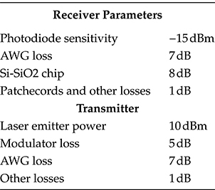
TABLE 9.9 Characteristics of the Preexisting 40 Gbit/s Line Where the 100 Gbit/s Signal Has to Be Accommodated
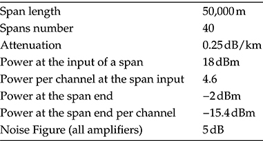
9.5.1.2 Penalty Analysis
9.5.1.2.1 Residual Chromatic Dispersion
The residual chromatic dispersion at the link end is 500 ps/nm, which is 275 ps in the bandwidth of 0.55 nm of the 8-DPSK signal.
The chromatic dispersion penalty induced on 8-DPSK transmission with self-beating detection has been analyzed in [71]. The procedure is the same outlined in Chapter 6. The ISI has to be taken into account by considering the memory effect introduced by chromatic dispersion.
The ISI reduces the dynamic range of the modulation in a deterministic way, thus the penalty can be evaluated as average EOP.
This penalty is plotted in Figure 9.48. From the figure it is derived that the line residual dispersion implies a penalty larger than 3 dB, which for sure cannot be considered small. Thus per channel dispersion compensation is needed.
This compensation is realized in two steps: a fiber-based per channel dispersion compensator is placed in front of the transponder (physically in the ad hoc subrack where are allocated the 100 Gbit/s transponders) to compensate 200 ps of chromatic dispersion with the correct slope, the remaining correction is realized via an electronic dispersion compensator. Using a high dispersion dispersion-compensation fiber (DCF), 200 ps are attained for a 33 GHz wide signal with about 4 km of fiber; thus both cost and occupied space are not very large even if this is a per channel compensator.
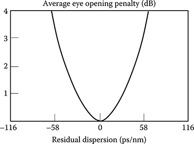
FIGURE 9.48 Chromatic dispersion-induced penalty in a 100 Gbit/s 8-DPSK with self beating detection. (After Seimetz, M. et al., IEEE J. Lightwave Technol., 25(6), 1515, 2007.)
This design is due to the fact that the electronic equalizer will be useful to compensate other ISI causes also, like PMD or some forms of nonlinearities, thus it has not to be overloaded by the need of compensating a great residual dispersion.
A study on design of electronic compensation in M-DPSK systems is reported in [72] where an optimized algorithm is proposed for small state number MLSE to be applied to M-DPSK systems.
To adapt to our case the results in [60] requires passing from a bandwidth of 20 GHz for a 4-DPSK at 40 Gbit/s to a bandwidth of 33 GHz from an 8-DPSK at 100 Gbit/s; this can be done by scaling the penalty taking into account the different distances on the phase circle between nearby constellation point and scaling the dispersion corresponding to a certain penalty of 1.65 2, which is about a factor 2.7.
The resulting penalty curve is shown in Figure 9.49, and for the residual dispersion of 75 ps the penalty is 1.25 dB.
9.5.1.2.2 Polarization Mode Dispersion
Under a qualitative point of view, the impact of PMD is the same suffered by other modulation format. A detailed analysis has been carried out in [74,75], taking into account both the average penalty and the outage probability due to instantaneous bad relation among the SPS and the transmitted polarization.
Also PMD of a standard SSMF has to be compensated and since an electronic dispersion compensator is already foreseen for the residual dispersion, the easier way is to design the compensator also for PMD compensation.
This is done in [72], adopting the MSLE already described in the previous section, the PMD related penalty results as in Figure 9.50. Thus, for Δτ=0.1√1500≈4ps![]() , the associated penalty is 0.25 dB.
, the associated penalty is 0.25 dB.
9.5.1.2.3 Kerr-Induced Degradation (SPM, XPM, and FWM)
The effect of SPM is considered in [71] in great detail. Naturally, the overall penalty depends both on the span input power (that is assumed the same for each span) and on the number of spans.
The SPM penalty plot deduced in the regime of small penalty per span is reported in Figure 9.51 taking into account also the mitigating effect of residual dispersion. The sensitivity to the nonlinear phase distortion due to SPM is greater for M-DPSK with respect to IM (see Chapter 6) due to the number of levels and to the fact that the information is coded in the phase; thus it is directly affected by the Kerr-induced phase fluctuations.
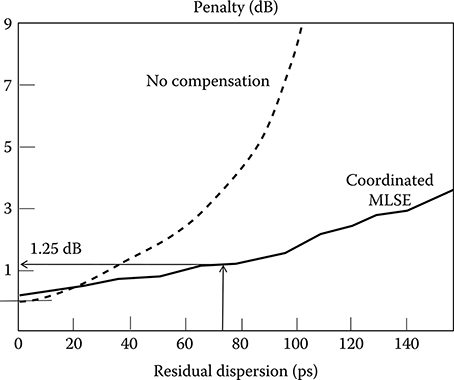
FIGURE 9.49 Penalty curve after optical and electronic residual dispersion compensation in the case of a 100 Gbit/s 8-DPSK system transmitted on a line designed for 40 Gbit/s. (After Salehi, J.G. and Proakis, M., Digital Communications, 6th edn., McGraw Hill, s.l., 2008.)
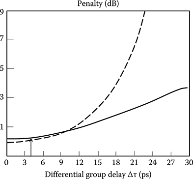
FIGURE 9.50 Penalty curve after electronic PMD compensation in the case of a 100 Gbit/s 8-DPSK system transmitted on a line designed for 40 Gbit/s.
(After Freckmann, T. et al., Joint electronic dispersion compensation for DQPSK, Proceedings of Optical Fiber Conference/International Optical and Optoelectronics Conference OFC/IOOC 2008, San Diego, CA, IEEE/OSA, s.l., 2008, p. OTuO.6.).
Nonlinear induced crosstalk can be classified as in case of IM systems in XPM-induced and FWM-induced crosstalk. In both cases, the decrease of the spectrum width with respect to the 80 GHz for which the system is designed helps alleviate the effect.
XPM-induced crosstalk is studied in [75] where it is demonstrated that, in our conditions, SPM is dominant. Nevertheless, XPM is particularly dangerous for this modulation format, due to the fact that the power is constant.
This can be intuitively understood looking at Equation 4.41 that expresses the nonlinear phase in the case of a WDM comb. While in the case that the intensity of the channels fluctuates, the walk off due to dispersion generates a mixed situation in which some channels do not contribute due to the absence of power; this does not happen in the case of a constant power modulation format.
Naturally, polarization fluctuations and phase differences due to walk off still work to reduce XPM efficiency, but in the same general situation, XPM is more efficient for constant power modulation formats.

FIGURE 9.51 SPM-induced degradation in the case of the 100 Gbit/s 8-DPSK transported on a 40 Gbit/s line. In the curves, the interplay of SPM with the residual dispersion is taken into account.
(After Seimetz, M. et al., IEEE J. Lightwave Technol., 25(6), 1515, 2007.)
Starting from the model reported in [75] and imposing the condition of small penalty, it is possible to determine the penalty in our conditions.
For high power channels, XPM causes a plateau, not differently from other power dependent effects, but in the range of the possible power in this class of systems, the penalty is so low that the plateau can be neglected.
As far as FWM is concerned, the same model used in Chapter 6 can be reapplied here: FWM-induced crosstalk can be considered as an additional noise, due to its variability that is almost random for the effect of the walk-off. Reapplying the evaluation of Chapter 6, the FWM-induced penalty results to be about 0.5 dB.
9.5.1.2.4 Linear Crosstalk
The analysis of the impact of the linear crosstalk can be done in complete analogy to what was done in Chapter 6 for IM systems. However it has to be taken into account that the worst case for linear crosstalk is constituted by a 100 Gbit/s channel with only 40 Gbit/s channels around, as a matter of fact, the binary 40 Gbit/s channels have a wider spectrum so causing higher linear interference.
The evaluation has been done with the method of [74] both for the case of all DPSK channels and for the case of a single 100 Gbit/s channel with 40 Gbit/s channels around. The penalty curve is plotted in Figure 9.52.
In our case, it results a penalty of about 0.15 dB for the case of complete substitution of the channels with 100 Gbit/s 8-DPSK (when Δω/2πRs = 6) and 0.3 in the case of an isolated 8-DPSK channel among a 40 Gbit/s comb (where Δω/2πRs = 5).
9.5.1.2.5 Penalty Analysis Summary
The summary of the penalty analysis is reported in Table 9.10. The estimated SNo required to reach the desired performances is 21 dB, smaller than the about 22.3 dB obtained from the draft design.
Second step is the simulation, which here is carried out considering the evolution of the deterministic part of the signal and adding the effect of noise analytically.
This confirms the effectiveness of the draft design and the fact that the 8-DPSK 100 Gbit/s signal performs quite better with respect to the original binary 40 Gbit/s signal for which the link was designed.
This is mainly due to the smaller value of the signal optical bandwidth, which is 33 GHz instead of 40 with a remarkable difference of 19%, but also the low value of the required SNe has its role.

FIGURE 9.52 Linear crosstalk-induced penalty both in case of a single 100 Gbit/s channel and in case of a complete substitution of all the channels with 100 Gbit/s.
TABLE 9.10 Summary of the Penalty Analysis for the 8-DPSK 100 Gbit/s Designed to Work with a Line Optimized for 40 Gbit/s NRZ
This example shown as 8-DPSK is quite promising for transmission of 100 Gbit/s signals on links designed for 40 Gbit/s.
9.5.2 Practical Multilevel Systems: Transmitting 100 Gbit/s on a 10 Gbit/s Line by 4QAM
This is a much more difficult problem with respect to that faced in the last section. In order to match the signal bandwidth for which the system is designed, the optical bandwidth should be reduced of a factor 10, and this means using 1024 levels at least.
However, similar to almost all the systems designed for 10 Gbit/s, our reference system also has an optical pass-band (essentially determined by the multiplexer and the demultiplexer) greater than the bandwidth of a 10 Gbit/s signal: as a matter of fact Moe = 2.
Since the available unilateral optical bandwidth is 20 GHz (the channel shape is approximately Gaussian) we can also accommodate a signal with a wider spectrum. As a trade-off between spectrum width and required signal to noise, we will choose a 64 levels 4QAM with a unilateral optical bandwidth of 16.6 GHz thus reducing Moe to 1.2.
The line data are summarized in Table 6.2.
9.5.2.1 Ideal Signal to Noise Ratio Requirements
The ideal SNe required to achieve an error probability of 10−12 can be deduced from Figure 9.42 for constant power 64-4QAM obtaining 21.8 dB.
The symbol rate is 16.6 Gsymbol/s, thus using NRZ transmission, the optical unilateral signal bandwidth is 16.6 GHz.
With the resulting value of Moe = 1.2, the required SNo is equal to 24 dB.
9.5.2.1.1 Power Budget
The parameters of the components that are used at the transmitter and at the receiver are reported in Table 9.11, where it is imagined that the receiver is built using Si-SiO2 chips as shown in Section 9.3.2.4.
At the transmitter, in order to overcome 15 dB of loss of modulator and transmitter passives, a high power external cavity tunable laser is selected, to assure 13 dBm of emitted power and a very small linewidth, which in line with the best commercial lasers we will assume equal to 500 kHz.
In this way, the power on the booster amplifier is −7 dBm per channel, that is 7.4 dBm total. This power needs an attenuation not to damage the booster, but it is good to face tolerances and aging.
At the receiver, the total receiver loss is 21 dB, which requires the use of an APD with a sensitivity of −25 dBm over an optical bandwidth of 20 GHz.
Fixing the power on the APD equal to −19.5 dBm to be able to neglect thermal and multiplication noise in the power budget, the power per channel at the preamplifier output is 0.5 dBm, for a total power at the preamplifier output of 20 dBm, the same power exiting from the preamplifier when the system works at 10 Gbit/s.
9.5.2.1.2 Draft Design SN Estimation
The estimation of the ASE limited optical signal to noise ratio can be carried out as in all the other cases: evaluating the ASE power in the line after the design.
In our case, the ASE power is −16.9 dBm, which provides an SNo of 17.5 dB at the preamplifier output in the assumed hypothesis for the channels power.
TABLE 9.11 Transmitter and Receiver Data for 1024-QAM Designed to Be Used on a 10 Gbit/s Line
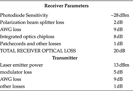
Adding an advanced FEC gain of 11 dB an SNo of about 28.5 dB is obtained, which is greater than the required value of 24 dB.
However, the difference between the power budget value, comprising the FEC gain, and the theoretical value is only 3.5 dB. So small a value does not allow a normal amount of penalties to be allocated, thus even if theoretically the system can work, in practice, it is not feasible due to nonideal propagation effects and to the margins necessary to take into account components characteristics fluctuations and aging.
In order to increase the SNo to allocate the penalties, it is needed to increase the power per channel along the line without increasing the noise. Moreover, the impact of nonlinear effects has to be carefully controlled.
This can be done in two ways: either regulating the line amplifiers and the preamplifier to increase the output power or decreasing the number of channels so that the available power can be distributed among fewer channels.
In both cases naturally, great attention has to be paid not to increase the power per channel too much to generate a high penalty due to nonlinear effects.
Here we imagine, as almost always in practical systems, that amplifiers configuration can be controlled within certain limits via the system element manager.
As already done in the case of 40 Gbit/s transmission (see Chapter 6), we reconfigure the in line amplifiers so to decrease the output power up to 18.5 dBm. Moreover we divide by half the number of channels fixing to 100 GHz the channel spacing. This contemporary increases the power per channel at the output of in line amplifiers up to 2 dBm and takes under control linear and nonlinear crosstalk that otherwise will increase due to the passage of the optical signal bandwidth from 10 to 16.6 GHz.
The resulting configuration conveys in any case the huge capacity of 4.5 Tbit/s, with an upgrade of a factor 5 with respect to the 900 Gbit/s of the original system.
The SNo calculated from the power budget increases to 30 dB, taking into account 11 dB of super FEC gain thus providing a margin of 5 dB to allocate penalties.
9.5.2.2 Penalties Analysis
As usual in this section all the relevant penalties coming from the different system impairments are evaluated and added to verify that the overall SNo is sufficiently high to guarantee a correct system working.
9.5.2.2.1 Transmitter Dynamic Range
Due to the small margin available, the transmitter is particularly accurate, reducing the dynamic range penalty from 1 dB, which is considered a standard transmitter performance, to 0.3 dB. This is done with an accurate balance of dual arms modulators used in the transmitter [32].
9.5.2.2.2 Linear Crosstalk
We have an optical bandwidth of the transmitted signal of 16.6 GHz with a spacing of 100 GHz and a Gaussian filter of 20 GHz. Thus the ratio between the optical bandwidth and the symbol rate is 1.2 and the normalized spacing is about 6. In this condition, repeating the procedure carried out in Chapter 6 where the linear crosstalk is considered like an additional noise source, a penalty of 0.2 dB is obtained.
9.5.2.2.3 Phase Noise
Both the used optical sources, the transmitting laser and the LO, are external cavity lasers, with a linewidth of 500 kHz.
The global linewidth to symbol rate ratio is then 3 × 10⁻⁵. In this condition, the phase noise is completely negligible.
9.5.2.2.4 Nonlinear Depolarization Effect
The depolarization occurring during fiber propagation due to Kerr effect is analyzed in [65,77]. Applying the method reported in [65] to our case, the propagation of a 16.6 GHz signal along 3000 km with a span length of 70 km and a power at the in-line amplifier output of 2 dBm, the depolarization factor δpol is about 0,0025.
Equation 9.81 can be rewritten as a function of the SNo, obtaining for our system working with a pre-FEC SNo equal to 19 dB a plateau due to nonlinear depolarization equal to 26 dB and a penalty due to depolarization equal to 0.9 dB.
The plateau is sufficiently far from the system working point, but the penalty is not so small, considering the small margin we have.
9.5.2.2.5 Nonlinear Crosstalk
Even if the power propagating along the line is quite high, the nonlinear crosstalk is limited by the increased channel spacing.
The impact of FWM can be estimated by the model detailed in Chapter 6 obtaining a penalty of 0.15 dB, while XPM results to be negligible
9.5.2.2.6 Residual Chromatic Dispersion, Self-Phase Modulation and PMD
Residual chromatic dispersion, SPM and PMD are the relevant ISI sources in this system.
As far as PMD is concerned, using the model of Chapter 6, it is easy to determine that the penalty due to PMD is completely negligible in this case (below 0.1 dB).
The situation is quite different regarding the interplay between SPM and DGD.
The system is designed optimizing the dispersion map for a transmission at 10 Gbit/s.
Thus postcompensation is used, with an under-compensation of 1020 ps/nm that in our case means an uncompensated dispersion of 141 ps. Taking into account that the transmitted pulses are 60 ps long residual dispersion requires per channel compensation.
Coherent detection renders available both amplitude and phase of the received signal so that very smart electronic processing is possible, simultaneously targeting the equalization of several impairments [51,78].
Here we will use a suboptimal design: that is, we will assume that the ISI equalizer (caring for chromatic dispersion, PMD, and any form of nonlinear ISI), the LO frequency locker, and the decision device are separated circuits that do not exchange information, but for the link between decision and frequency lock.
As a matter of fact, decision driven frequency lock is operated so that the decision device provides a feedback to the frequency lock control signal generator. A wide review of all the available alternatives that is very useful to analyze other design possibilities is reported in [77].
As far as the ISI equalizer is concerned, we will assume to use a small number of states MLSE with the objective to compensate all the ISI deriving from the interplay between residual dispersion and SPM.
Such an MLSE can be based on a small number of sample per bit; in literature it is clearly demonstrated that a number of samples greater than 4–5 per bit interval is of small utility if the number of states of the MLSE is not huge [78] and three samples seems to be the optimum value for small states MLSE [79].
Thus a sampling rate of 50 Gsamples/s is assumed, which is within the reach of very fast 32 nm CMOS electronics, as demonstrated by literature on predistortion compensation (see Chapter 5).
A very general method for the evaluation of the performances of an MLSE in the case of multilevel transmission is reported in [79]. This can be applied in our case with suitable modification that takes into account both the different receiver and the modulation format.
The results presented here can be compared with those in [79] taking into account that, in a very first approximation, the ISI-induced penalty depends only on the ratio between the pulse broadening and the pulse width and on the distance between first neighbors in the signal constellation. This is evident also from the data reported in [79].
Thus, the penalty due to ISI for quadrature coherent detection can be plotted introducing the ISI index already used in the previous section as the ratio between the pulse broadening Δτ and the pulse width TS = 1/RS.
Considering a 16 states MLSE and a 4 states MLSE, as described in [79], the ISI-induced penalty is represented in our case in Figure 9.53 for different numbers of MLSE states.
In order to use data in Figure 9.53, the ISI index has to be related to the physical parameters of the link, taking into account the interplay between SPM and chromatic dispersion.
In our case, we are propagating an NRZ signal. The pulse broadening due to the interplay between SPM and dispersion can be simulated and since this effect depends on the pulse energy, the broadening will be different from pulse to pulse since different energies are transmitted in correspondence to different symbols.
This effect could be taken correctly into account by evaluating the broadening for each pulse of the constellation and defining a different error probability for different symbols. For sake of simplicity, and also since a very detailed analysis of this effect is not so useful due to the great number of other approximations, we will simply consider the worst case broadening. The worst case could be not relative to the most powerful pulse, depending on the partial compensation between SPM and dispersion at the different powers; all the constellations have to be considered in any case (compare Chapter 6).
The ISI is plotted versus the power at the input of a span in Figure 9.54 that is obtained by simulating the propagation of a single pulse through the line. From the figure, it is evident that an optimum system working point exists, as anticipated in Chapter 4, in correspondence of which the pulse broadening is minimum due to the interplay between SPM and DGD. In this case, the optimum transmitted power is about 0 dBm.

FIGURE 9.53 Penalty due to ISI versus the ISI index for different types of low number of states MLSE. (After Alfiad, M.S. et al., IEEE J. Lightwave Technol., 27(20), 4583, 2009.)
FIGURE 9.54 ISI index versus the power per channel at the input of a span.
The system however cannot work with this low transmitted power, which does not assure a sufficient SN to be attained. Thus a greater ISI has to be accepted. At the power at the span input equal to 2 dBm, the ISI factor is about 0.45, that is, the pulse width increases almost 50%.
From Figure 9.53, if we select an MLSE with 16 states, this ISI factor implies a penalty of 0.1 dB.
9.5.2.2.7 Penalties Analysis Summary
The summary of the penalty analysis relative to this case is reported in Table 9.12, the resulting pre-FEC SNo is 18.65 dB, slightly smaller than the 19 dB deriving from the draft design, thus suggesting that the system is feasible.
In this case, simulation is particularly important due to the small margin between the draft design and the result of the penalties analysis.
As usual we have performed a simulation of all deterministic phenomena adding the noise through a theoretical model. The simulation result completely confirms the analysis, providing a situation slightly better than that depicted by the penalty analysis, confirming that the bulk of the adopted approximations are worst cases.
9.5.3 Practical Multilevel Systems: Transmitting 100 Gbit/s on a 10 Gbit/s Line by PolSK
In the above section, we have designed the 100 Gbit/s system so that the spectrum fits into the available optical bandwidth. This has brought us to use a great number of levels, with the consequent complexity at the system terminals and the need of maintaining a high line power to achieve the required high SNo.
In the following section, we will select another option: we will accept a strong distortion of the 100 Gbit/s signal due to system filters that we will then try to recover through an ISI equalizer.
This will allow us to maintain the number of levels lower thus simplifying the system terminals.
9.5.3.1 Draft Design and Power Budget
Reducing the number of levels quite below 64 means to increase the bandwidth above the value for which the system has been designed thus causing pulse distortion due to narrow optical filtering.
Thus pulse spreading due to tight optical filtering increases the ISI parameter and, with a suitable design of an equalizer, it could be at least partially corrected at the receiver.
TABLE 9.12 Transmitter and Receiver Data for 8-DPSK Designed to Use a 10 Gbit/s Line

The unilateral bandwidth of the signal generated after 8-PolSK modulation is around 33 GHz, against the 20 GHz available on the line (the system is designed with Moe = 2 for a 10 Gbit/s channel).
9.5.3.1.1 Ideal SNe and SNo
In this case, the required SNe to reach an error probability of 10−12 can be deduced from Figure 9.43 resulting to be 20.7 dB.
Also in this case, the corresponding SNo can be obtained in the usual way since Moe is smaller than one, but with greater than 0.5 (in a very first approximation the ratio between the optical bandwidth and the electrical one is 0.61). As a matter of fact, beyond 0.5 the equation we are using to relate the optical and the electrical SN is no more valid.
The requirement in terms of ASE-limited SNo results to be 25.8 dB.
9.5.3.1.2 Power Budget and Polarization Dynamics
In order to try a design using Direct Detection, we will select interferometric receiver. The relevant characteristics of receiver components are summarized in Table 9.13; all the power budget equations are fulfilled as can be easily derived.
TABLE 9.13 Transmitter and Receiver Data for 8-PolSK Designed to Use a 10 Gbit/s Line
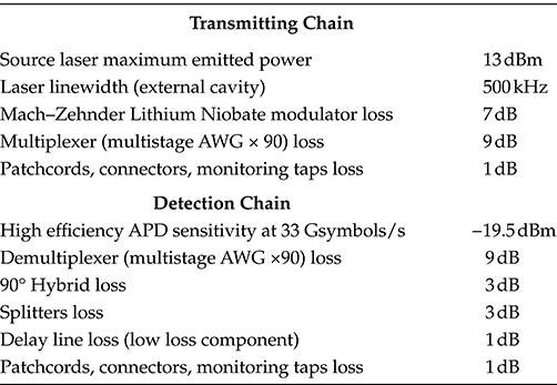
The situation would be very similar if the coated diodes receiver would be chosen.
The ASE power in the signal bandwidth is −15.4 dBm so that SNo = 17.44 dB.
This value, even after the addition of 11 dB gain of a super-FEC, is only a bit higher than the required 25.8 dB leaving no sufficient margin for the penalties allocation. As a matter of fact we have to expect at least 6 dB of penalties and margins.
In order to increase the power budget we can follow the same line used for the 4QAM and cut by half the number of channels.
Changing two 10 Gbit/s channels with one 100 Gbit/s, a comb of 100 GHz spaced channels at 100 Gbit/s is obtained formed by 45 channels as in the case of 64-4QAM.
This allows, with an amplifier output power slightly reconfigured from 20 to 20.5 dBm, to bring the power per channel at the preamplifier output to 4 dBm, bringing the SNo from 17.44 to 21 dB.
So high a power per channel, however, creates a very detrimental effect for a polarization modulated system.
Applying the method reported in [65] to our case, the propagation of a 33 GHz signal along 3000 km with a span length of 70 km and a power at the in-line amplifier output of 4 dBm, the depolarization factor δpol is about 0,01.
Equation 9.28 tells us that, every time there is a part of the information coded in the field polarization, that is, every time there is the need of polarization tracking, high speed polarization fluctuations introduces a plateau in the SNo and thus in the BER. This plateau is expressed by Equation 9.28 itself.
The only way to avoid this plateau would be to increase the speed of the polarization tracker to follow these fast fluctuations also, but in the case of Kerr-induced depolarization this is not possible due to the speed of the effect.
In our case, the plateau is 20 dB; thus nonlinear polarization fluctuations set an upper limit to the system SNo that is too low to allow transmission at 3000 km.
The only way to go is to cut the link length.
In order to do that, let us imagine placing a double terminal in an intermediate site to regenerate all the signals at half the length.
In this situation, maintaining 90 channels at 100 Gbit/s, we have two identical systems 1500 km long with a capacity of 9 Tbit/s.
Maintaining the amplifiers output power at 21 dBm, the power per channel at the input of a span is 1.45 dBm and the depolarization index is δpol = 0.0012 for a limit SNo = 29.2 dB, a quite high number.
The effective value of the SNo estimated through the power budget and the noise power evaluation is 21.6 dBm that becomes 32.6 after the super-FEC gain.
This leaves a margin of 5.5 dB for the allocation of the penalties. This margin is not very high, but should be sufficient in our case.
Also in this shorter configuration, it is easy to demonstrate that with the figures reported in Table 9.13, the power budget equations are satisfied both at the receiver and at the transmitter.
9.5.3.2 Penalties Analysis
9.5.3.2.1 Intersymbol Interference (Residual DGD, SPM interplay, PMD, Optical Filtering)
ISI is mainly caused by three factors:
SPM and residual dispersion interplay
PMD
Tight optical filtering
In a regime of small pulse distortion we will assume that the overall ISI index can be obtained from the individual contributions.
Dividing SPM and dispersion from PMD we can write
pout(t)=ˆAreˆPˆK^Atrpin(t)(9.84)
![]()
(9.84)
where the four operators acting on the envelop of the input pulse pin(t) are: the transmitter AWG (Ätr), the receiver AWG (Äre), the interplay between dispersion and SPM taking into account in-line compensation ^(K)![]() , and the PMD ^(P)
, and the PMD ^(P)![]() .
.
To each process is associated a pulse spreading τ so that, for example,
τ2re=∫t2ˆArepin(t)dt−T2(9.85)
![]()
(9.85)
where T is the width of the original pulse. Since NRZ pulses are symmetric around their axis and the first filter of the chain is Gaussian (thus symmetric too) the overall pulse broadening can be found in a first approximation using the formula
τout=√τ2re+τ2p+τ2k+τ2tr(9.86)
![]()
(9.86)
as graphically show in Figure 9.55. This rule is rigorously true for a cascade of linear processes with one nonlinear instantaneous process (see Appendix 3). Here we approximate our model assuming a concentrated effect for the interplay between SPM and dispersion, while they are distributed phenomena.
This will allow us to proceed with the penalty analysis considering the different causes of ISI separately.

FIGURE 9.55 Approximation used to evaluate the overall ISI index of the system. (a) Physically, all the ISI-related phe-nomena works in series; (b) in the approximation they work in parallel and at the end, the pulse widening are added.
The analysis can be done with the same methods used for IM systems (see Chapter 6), taking into account the fact that the rapid polarization fluctuations decrease the SPM efficiency. The ISI index in our case for 8-PolSK is reported in Figure 9.56.
The influence of PMD results to be negligible, as it can be demonstrated evaluating the ISI index by multiplication of the PMD parameter by the system length and comparing with the symbol interval.
As far as the ISI index is relative to optical filtering it can be determined by simulation by simply reconstructing the relevant signal and filtering it with the filter transfer function simulating the cascade of optical filters along the transmission line (essentially the two AWGs).
The ISI index deriving from the too narrow filtering is reported in Figure 9.57.
At this point, even from a simple look at the ISI indexes, it is quite clear that transmission cannot happen without an ISI equalization.
The first choice for our design would be an MLSE. Unfortunately, the balanced MLSE requires at least three samples per symbol; thus a minimum sampling rate of 99 Gsamples/s would be required, that currently is beyond the possibility of so complex a circuit.
This consideration not only excludes the MLSE, but also all the digital compensation strategies at the receiver, which needs oversampling of the received signal.

FIGURE 9.56 Normalized ISI index due to the interplay between SPM and chromatic dispersion in our 8-PolSK transmission example.

FIGURE 9.57 Normalized ISI index due to tight optical filtering in 8-PolSK assuming Gaussian filtering.
(After Jiang, Z. et al., Nat. Photon., 1, 463, 2009.)
The only possible solution is an analog per channel compensation. A very interesting method that can solve this kind of problems has been presented in [80]. The idea is to use an optical pulse shaper to predistort the optical signal at the transmitter in order to obtain the wanted pulse shape.
An AWG is used as spectrum analyzed so that, once the spectral components of the transmitted signal are separated, they can be filtered with an amplitude and phase mask to create an approximation of the Fourier transform of the wanted pulse. After that, the spectral components are recombined with another AWG.
If only small changes in the channel characteristics has to be compensated, the intensity and phase masks can be tuned, for example, by temperature controller, if fast channel estimation and tracking is needed, they can be substituted with modulators controlled by a DSP.
The scheme of this optical per channel compensator is presented in Figure 9.58 [81]. The entire pulse shaper has been also realized in a single InP-based monolithic chip, demonstrating the potentiality of this technique [82].
In principle, the chosen solution can compensate whatever amount of ISI can be generated; in practice the amount of ISI that can be compensated is limited by both component and system limitations.
The main limitations to the compensation method efficiency are the imperfect AWG working that causes the produced set of fields to deviate from the components of the Fourier transform of the input field, the needed approximation intrinsic in working with a discrete number of spectral components, and the presence of nonlinear propagation.
Let us call F0(ω) the ideal Fourier transform of the impulse to be transmitted, so that at the receiver it is compressed to completely eliminate the ISI.

FIGURE 9.58 Block scheme of per channel optical pulse shaper used to compensate ISI.
(After Jiang, Z. et al., Nat. Photon., 1, 463, 2009.)
The waveform generator approximates F0(ω) with the following function
F(ω)=rectΩ(ω)v/2Σj=−v/2[F0(jΔω)+ϕj]GΔω(ω+jΔω2)(9.87)

(9.87)
where
Ω is the global bandwidth
GΔω(ω) represents the AWG response
Δω is the step between two consecutive frequency samples, while the number of samples is equal to v +1.
Imagining to realize the pulse shaper with an InP integrated circuit, ϕj is the processcaused intrinsic error in reproducing the complex numbers F0(j Δω).
The potential performance of the precompensation method depends on the bandwidth and the number of samples at the AWG output, besides the precision with which the complex values F0(j Δω) are reproduced by the intensity and phase masks/modulators.
In Figure 9.59, an example of the ability of a pulse shaper based on Gaussian AWGs is shown. In Figure 9.59a, the spectrum to be reproduced is shown, while in Figure 9.59b it is superimposed to the spectrum at the output of the shaper of Figure 9.58 that is assumed to be realized with 100 frequency slices and Gaussian AWGs. The simulation parameters are an optical bilateral bandwidth of 200 GHz and typical tolerances for InP Mach–Zehnder Modulators that uses similar technology steps.
Since the configuration above is quite near to an ideal shaper even with practical parameters, it results that the main limitation to the compensation capability of this method is due to nonlinear effects.

FIGURE 9.59 Example of the shaper accuracy in reproducing a complex spectrum: (a) test spectrum to be reproduced; (b) comparison of the spectrum created by the shaper with the original spectrum; (c) particular of one of the spec-trum peaks where the maximum error is located if the tails far from the main spectrum band are not considered.
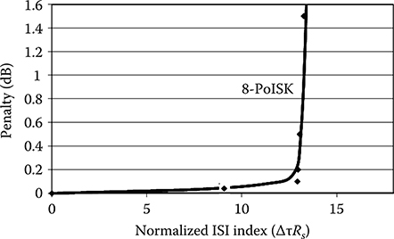
FIGURE 9.60 Residual penalty after pulse optical precom-pensation versus the ISI normalized index.
Passing through all the states from the predistorted form and the final form, the pulse presents in correspondence to some link sections sharp peaks that creates a great amount of nonlinear effect. These are not simulated when the final shape of a normal transmitted pulse is inverted to find the correction function; thus the shape of the predistorted pulse is not perfect.
This is also the cause of an expected marked difference between the behavior of phase modulation and polarization modulation. Polarization modulation is practically a form of double amplitude modulation and the impact of the nonlinear phase variations are less evident when the predistorted pulse propagates along the fiber link.
Passing to the compensation capacity, it has been assessed by simulation of the deterministic part of the single channel fiber propagation through the link that we are considering with a split step algorithm to determine the output pulse distortion.
This has been precompensated by a suitable transfer function and the output SNo penalty has been derived and plotted in Figure 9.60.
Since the technology errors ϕj are random variables, the penalty curves plotted in the figure are worst case curves, where all the errors are in the same direction and at the 3σ point of their distribution.
The compensation capability of the method is impressive: to arrive to have a penalty of 3 dB the pulse has to broaden in noncompensated propagation up to 13 times its initial width: no practical postcompensation would be capable of doing that.
At this point, all the elements are available to evaluate the ISI penalty.
The ISI index due to the interplay between chromatic dispersion and SPM is about 0.9 while, as far as the tight filtering is concerned, the relative bandwidth is 0.6, implying a relative ISI index of 0.3.
Applying the ISI indexes summation rule, which holds with so small indexes, the total ISI is 0.95.
From Figure 9.60, we see that at such ISI, the optical compensator works very well and the residual penalty is lower than 0.1 dB.
9.5.3.2.2 Linear Crosstalk
Linear crosstalk is very important, due to the large spectra of the chosen modulation formats with respect to the channel spacing that is determined by the already deployed system.
A penalty of 1.0 dB is evaluated using the same model introduced in Chapter 6.
9.5.3.2.3 Nonlinear Crosstalk (FWM and XPM)
Chromatic dispersion under compensation makes XPM to be less efficient. However, the effectiveness of this design tool is not as good as in the case of 10 Gbit/s due to the fact that the dispersion map results are not optimized for the new modulation formats.
Applying the same model we have applied in Section 9.3.5, we derive in any case a negligible XPM penalty.
As far as FWM is concerned, the same model used in Chapter 6 can be reapplied here and the FWM-induced penalty is evaluated equal to 0.1 dB.
9.5.3.2.4 Nonlinear Polarization Fluctuations
If nonlinear polarization fluctuations are present, they have a smaller effect with respect to the case of coherent detection. As a matter of fact the fast fluctuations of the Jones matrix that cannot be tracked by the tracking circuit are due to its tight bandwidth.
Thus the overall effect is to smooth the Stokes parameters of a factor (1 − ρpol) and to transfer a part of the signal power proportional to the depolarization ratio to the noise.
Besides the plateau we have already introduced, the penalty relative to the depolarization can be written as in Equation 9.81 resulting to be 0.6 dB.
9.5.3.2.5 Summary of the Penalty Analysis
The results of the penalty analysis are summarized in Table 9.14.
At the end of the penalty analysis, the required SNo is exactly identical to that evaluated by the draft design.
TABLE 9.14 Summary of the Penalty Analysis for the 8-DPSK and 8-PolSK 100 Gbit/s Designed to Work with a Line Optimized for 10 Gbit/s NRZ
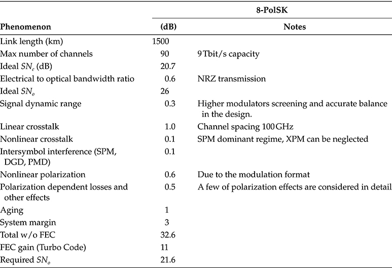
This lack of margin is not really important since we have to remember that a margin of 3 dB is already inserted in the penalty analysis. On the other hand, the simulation is a bit better than the penalty analysis, confirming the system feasibility.
9.5.4 Practical Multilevel Systems: Native 100 Gbit/s Ultra-Long Haul Systems
The last dimensioning exercise we will do is the design of a native ultra long haul 100 Gbit/s system.
9.5.4.1 Draft Design
We will use Raman-assisted transmission and the scheme of the generic system span will coincide with that of Figure 9.61, a familiar scheme from Chapter 6, but without inline Erbium Doped Fiber Amplifiers (EDFAs). The only EDFA is present as booster at the transmitter.
The intention is to limit the ASE as much as possible and to maintain a low power along the line to control nonlinear effects.
We will also adopt a span length of 30 km in order to decrease the ASE power as much as possible.
The line results to be composed of 257 spans, each of which is formed by 30 km of SSMF and 5 km of DCF pumped to obtain Raman gain. The Raman pumps are extracted at the DCF end so that propagation in the SSMF is completely passive.
The whole system is thus 9000 km, long. Since the design is inspired to a submarine application, no OADM is foreseen in the nodes.
As far as modulation is concerned, we select constant power 16-4QAM with coherent homodyne receiver. The value of the electrical signal to noise ratio allowing to reach a BER of 10−12 is in this case SNe = 17.5 dB, really a low value for a 16 levels modulation format. The unilateral optical bandwidth of the signal is 25 GHz while the overall channel bandwidth as seen by the single channel is 38 GHz so that Moe = 1.5 and the required optical signal to noise ratio is SNo = 18.7.
Due to the fact that the signal has a 25 GHz large spectrum on each side of the carrier, the channel spacing is selected to be 100 GHz, so that 45 channels are transmitted in the extended C band.
Precompensation is adopted, placing the DCF at the transmitter, and a residual dispersion of 1000 ps/nm is left to compensate channel by channel to partially counterbalance nonlinear effects during propagation.

FIGURE 9.61 Block scheme of the line site of the Ultra Long Haul 100 Gbit/s system presented in this chapter.
TABLE 9.15 Transmitter and Receiver Data for an Ultra Long Haul System at 100 Gbit/s Adopting Constant Power 16-4QAM with Coherent Detection

9.5.4.1.1 Power Budget and SNe
The main parameters of the components at the transmitter and at the receiver are reported in Table 9.15. With 16 dBs emitted power and a transmitter loss of 20 dB, the power at the booster input is 11.5 dB that is sufficient to saturate the booster without damaging it.
The booster gain results to be 6 dB and at the booster output and at the input of every span after the precompensation and preamplification, the signal power is 2 dBm per channel, that is, 18.5 dBm total power.
At the receiver, the EDFA preamplifier is not needed since the Raman stage provides all the needed gain of 17.5 dB, being dimensioned the same way of the in-line Raman amplifiers.
Moreover, a good APD has the required sensitivity at 25 Gsymbols/s to satisfy the power budget.
The pumps of the Raman amplifiers can be optimized both for flatness and for gain; however, also gain flattening filters with a very low loss (1.5 dB) are foreseen to improve the gain flatness.
The design SNe results to be 22.4 dB, with a great margin with respect to the ASE limited value of 17.5 dB.
This is mainly due to the small value of the span bringing the system nearer to the optimum design that would be a continuous distributed amplification (see Chapter 6). Just to verify this fact, if the design is done again with a span of 70 km, the SNe goes down to 15 dB, rendering in practice the transmission impossible.
It is to be observed that, under an SN point of view, the system could be much longer, up to 10,000 km and more. Moreover, a quite higher SN is achieved by slightly increasing the power at the span input. For example, bringing the power per channel at the span input at 3 dBm and the system at 10,000 km, the SNe is 25.78, better than that we have now.
Both these improvements are impossible due to nonlinear effects, mainly SPM and nonlinear polarization rotation, which are the main limitations to the system performances.
9.5.4.2 Penalties Analysis
The penalties analysis in this case presents several new elements with respect to what is done in Chapter 6 and in the previous sections.
9.5.4.2.1 Linear Crosstalk
The analysis of the impact of the linear crosstalk can be done in complete analogy to what was done in Chapter 6 for IM systems. In our case, the channels are quite near (100 GHz with a symbol rate of 25 Gsymbols/), thus even if the Gaussian filters are quite tight, the linear crosstalk penalty is quite high, of the order of 1.0 dB.
9.5.4.2.2 Residual Chromatic Dispersion, Self-Phase Modulation, and PMD
The link as it is designed uses dispersion under-compensation to balance at least in part the SPM phase shift. The residual dispersion of 1500 ps/nm requires per channel dispersion compensation.
We repeat here the assumption already done for the 64-4QAM to maintain decision and ISI compensation independent and to adopt decision driven LO phase lock.
Also in this case, a small number of states MLSE is suitable to correct the ISI coming from different dispersion sources and from SPM.
A sampling rate of 75 Gsamples/s is assumed, which should be within the reach of very fast 22 nm CMOS electronics.
Following the same procedure already used for 64-4QAM, the relation between the ISI index and the penalty after equalization is represented in Figure 9.53.
Moreover, the ISI index due to PMD and to the interplay between DGD and SPM are reported in Figures 9.62 and 9.63.
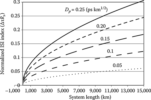
FIGURE 9.62 Pulse broadening due to PMD: ISI index versus the link length for different values of the PMD parameter.

FIGURE 9.63 Inter-symbol interference due to interplay between SPM and DGD in the Ultra Long Haul 100 Gbit/s system considered in the text: ISI index versus the transmitted peak power per channel.
Figure 9.63, obtained by the simulation of nonlinear pulse propagation, and considering that it takes into account the interplay between dispersion and SPM, indicates an optimum power for which the ISI index is minimum.
In our case, the residual dispersion is quite high (1000 ps/nm) and the effective link length defined regarding nonlinear effects is of the order of 3598 km (257 spans and 14 km per span).
In these conditions, with a bilateral signal bandwidth of 50 GHz, both SPM and dispersion have a strong broadening effect inducing chirps with opposite sign so that the compensating effect is evident.
The best working point is around 2 dBm, which is exactly the chosen working point for our system.
However, even at the best point, the link is so long that the pulse in free propagation completely loses its shape and widens more than 50%.
Summarizing, at 2 dBm per channel, the ISI index is 1.5 due to SPM and chromatic dispersion and 0.25 due to PMD, for a global ISI index of 1.55.
From Figure 9.53, we conclude that adopting a 16 states MLSE, the corresponding penalty is about 0.2 dB.
9.5.4.2.3 Nonlinear Crosstalk: XPM and FWM
Also in this case, following [75], the system is in the SPM-dominated regime due to the adopted chromatic dispersion map.
As far as FWM is concerned, the same model used in Chapter 6 can be reapplied here: FWM-induced crosstalk can be considered as an additional noise, due to its variability that is almost random for the effect of the walk-off.
The effect of both XPM and FWM are however enhanced by the channel proximity, by the great bandwidth, and by the long distance. Globally, the FWM penalty is 1.3 dB and the XPM penalty is 0.4 dB.
9.5.4.2.4 Transmitting Laser and Local Oscillator Phase Noise
We will imagine using external cavity tunable lasers and, as a reference, we will assume the lasers parameters values listed in Table 5.5. The linewidth listed in the table is 550 KHz, really small with respect to the symbol rate of 25 Gsymbols/s. In our case, Δν/Rs = 0.0002%. Looking at Equation 9.46 we see that the phase noise plateau is well beyond 55 dB, meaning, that at the required values of SNe, the phase noise induces only a small power penalty that from Equation 9.78 can be evaluated in 0.1 dBm.
9.5.4.2.5 Depolarization due to PMD and Nonlinear Propagation
The analysis of the behavior of δPOL where a WDM signal propagates through the fiber has been carried out in [65,77].
In particular, applying the methods developed in [65] to the present case, the plot reported in Figure 9.64 is obtained for the penalty due to the depolarization.
In the case under analysis where the power per channel at the span input is 2 dBm, the depolarization due to nonlinear effects is 0.0065.
The plateau due to depolarization is located for this value of δPOL at SNo = 21.8 dB, thus it is very near to the system working point, even if both the dispersion map and the transmitted power are optimized.
However, taking into account the gain of a super FEC of 11 dB and the value of 17.5 dB of ASE-limited required SNe, a careful design should manage to make the system work.
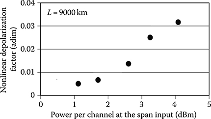
FIGURE 9.64 Nonlinear depolarization factor in the 9000 km 16-4QAM system under analysis versus the power at the input of the span.
The penalty derived from the nonlinear polarization evolution is 3 dB and it is by far the largest penalty. In the presence of so large a penalty, the penalty addition rule in principle does not hold.
However in this case, this is the only penalty that is so high; so we will go on assuming that the penalties can be added, using the simulation of signal propagation as validation test.
9.5.4.2.6 Polarization-Dependent Losses
A slight amount of polarization dependent loss is always present in transmission systems due to both slightly misaligned connections and to components characteristics [83].
Due to the critical system design, this point has to be considered in detail and not included into the margins.
As a matter of fact, polarization dependent losses have a strong impact on all the very high performance systems where part of the information is coded into the field polarization [85,].
The penalty due to the polarization dependent loss can be analyzed as in [84] as a function of the unbalance between the average amplitudes of the received field components along the reference polarization unit vectors.
The analysis shows that in order to maintain the penalty within 0.5 dB it is needed to maintain the unbalance within 2.5% with typical components parameters and system assembly accuracy, that is, to have a dichroism ratio (ratio between the difference of the two polarization components power and their sum) within −19 dB.
9.5.4.2.7 Penalties Analysis Summary
The summary of the penalties analysis is reported in Table 9.16.The required SNo results to be 18.8 dB.
The draft design value is 22.4 dB, thus the system seems feasible.
Nevertheless, it is a key point to verify the assumptions by simulation. From simulation, the required SNo results to be about 2 dB lower than that generated by the penalty addition rule, showing the fact that we are at the limits of validity of this method.
Analyzing simulation data, we can see that several points emerge where different phenomena interact. The main interactions are
All forms of crosstalk are a bit less effective due polarization fluctuations, channel asynchronous clock, and nonlinear polarization fluctuation
The worst case model for the linear crosstalk results to be too pessimistic
Also the FWM penalty model results to be pessimistic mainly due to the walk-off caused by polarization fluctuations
TABLE 9.16 Summary of the Penalty Analysis for the 100 Gbit/s Ultra Long Haul System Adopting Constant Power 16-4QAM with Coherent Detection

9.6 Summary of Experimental 100 Gbit/s Systems Characteristics
Since currently there is no diffused offering of products for long distance transmission at 100 Gbit/s we cannot provide the list of realistic characteristics generated from a synthesis of the characteristics of real products.
Thus, we will do a sort of summary of a few experimental implementations of high speed optical transmission.
In Table 9.17, a few experiments using multilevel modulation are summarized. In all the cases, but the first, PDM is used, that is, two channels are sent on orthogonal polarizations and on the same bandwidth.
It is easy to observe that the signal produced, just for an example, using PDM 16-QAM is not so different from a 256-4QAM obtained by the Cartesian product of two 16-QAM constellations, but for the fact that the signals on the coordinate plans (e1, e2) and (e3, e4) are synchronous in time in the 256-4QAM transmission, while they are asynchronous in the case of PDM 16-QAM.
For 256-4QAM obtained with full QAM constellations, we see that the normalized minimum distance is 0,111 while it is 0,471 for one of the QAM channels.
As a matter of fact, the absence of correlation between the transmitted constellations destroy the capability of 256-4QAM to compress the signal bandwidth of a factor eight at the expense of a reduction in the receiver sensitivity, while PDM simply transmits two channels in parallel, each of which reduces the bandwidth only of a factor four but has also the sensitivity of a format with much less levels.
TABLE 9.17 Review of the Main Features of a Few 100 Gbit/s Experiments Using Instantaneous Multilevel Modulation

A common factor for all the experiments presented in the table is the coherent detection. As a matter of fact, the additional sensitivity provided by coherent detection is an important plus in 100 Gbit/s systems.
Coherent receiver is generally realized by digital signal processing, so that an Analog to Digital converter at a speed of the order of 50 GHz is generally employed immediately after the detection.
In the table, there is one Ultra Long Haul system, conveying an impressive capacity by the use of both C and L band.
The line site of this system is exactly like the scheme of Figure 6.28, but for the presence of three Raman pumps, which are needed to have a flat gain over all the huge exploited bandwidth, and the fact that two EDFA in parallel provides gain in C and L band. The long span (90 km) is compensated by the very low attenuation fiber (0.166 dB/km).
The first two systems presented in the table are for long haul application. The first experiment is interesting since its scope was not to transmit a huge capacity but to verify what dispersion compensating scheme is optimum for such a system. The result, achieving the performances reported in the table, was that the optimum performance is attained by electronic equalization via nonlinear equalizer without any DCF in line.
It is possible that this result depends on the particular system scheme, a low number of channels, recirculating loop, and so on; in any case it is an interesting suggestion.
The third system is a sort of prototype of a potential long haul native 100 Gbit/s system, showing all the potentialities of the employed technologies.
The fourth system is a long single span system. It uses the remote Raman pumping technique with an impressive Raman pump injecting 5.5 W power into the fiber to create gain of about 140 km far from the end terminal.
The fourth system is a demonstration of the possibility to go beyond 100 Gbit/s, with a comb of 175 Gbit/s channel transmitted on more than 400 km of fiber.
REFERENCES
1. Shabtay, G., Mendlovic, D., Itzhar, Y., Optical single channel dispersion compensation devices and their application, Proceedings of European Conference on Optical Communications ECOC 2005, Glasgow, U.K., Vol. 3, pp. 321–323, 2005.
2. Drummond, M. V. et al., Tunable optical dispersion compensator based on power splitting between two dispersive media, IEEE Journal of Lightwave Technology, 28(8), 1164–1175 (2010).
3. Ikuma, Y., Tsuda, H., AWG-based tunable optical dispersion compensator with multiple lens structure, IEEE Journal of Lightwave Technology, 27(22), 5202–5207 (2009).
4. Seno, K. et al., Tunable optical dispersion compensator consisting of simple optics with arrayed waveguide grating and flat mirror, IEEE Photonics Technology Letters, 21(22), 1701–1703 (2009).
5. Seno, K. et al., 50-Wavelength channel-by-channel tunable optical dispersion compensator using combination of arrayed-waveguide and bulk gratings, Conference on Fiber Communication (OFC), Collocated National Fiber Optic Engineers Conference, 2010 (OFC/NFOEC), San Diego, CA, IEEE/OSA, s.l., pp. 1–3, 2010.
6. Yang, K., Liu, J., Zeng, X., Electronic dispersion compensation for PMD in 40-GB/s optical links, Communications and Photonics Conference and Exhibition (ACP), Shanghai, China, IEEE, s.l., pp. 1–2, 2009.
Sunnerud, H., Karlsson, M., Andrekson, P. A., Analytical theory for PMD-compensation, IEEE Photonics Technology Letters, 12(1), 50–52 (2000).
8. Lid, X., Xie, C., van Wijngaarden, A. J., Multichannel PMD mitigation through forward-error correction with distributed fast PMD scrambling, Optical Fiber Communication Conference (OFC 2004), Los Angeles, CA, IEEE, s.l., Vol. 1, pp. WE2 1–3, 2004.
9. Liu, X., All-channel PMD mitigation using distributed fast polarization scrambling in WDM systems with FEC, Conference on Optical Fiber Communication and the National Fiber Optic Engineers Conference, 2007, OFC/NFOEC 2007, Anaheim, CA, IEEE/OSA, s.l., pp. ONH4 1–3, 2007.
10. Klekamp, A., Werner, D., Bülow, H., Study of different 40Gbit/s FECs regarding PMD mitiga-tion efficiency by fast polarization scrambling, Conference on Optical Fiber Communication and the National Fiber Optic Engineers Conference, 2008, OFC/NFOEC 2008, San Diego, CA, IEEE/OSA, s.l., p. JWA54, 2008.
11. Bulow, H., Limitation of optical first-order PMD compensation, Optical Fiber Communication Conference, 1999, and the International Conference on Integrated Optics and Optical Fiber Communication, OFC/IOOC ‘99, San Diego, CA, Technical Digest, IEEE/OSA, s.l., Vol. 2, pp. 74–76, 1999.
12. Midrio, M., First-order PMD compensation in nonlinearly dispersive optical communication systems via transmission over the principal states of polarization, IEEE Journal of Lightwave Technology, 17(2), 2512–2515 (1999).
13. Linares, L. C. B., von der Weid, J. P., Comparison of first order PMD compensation techniques, Proceedings of the Microwave and Optoelectronics Conference, 2003, IMOC 2003, Parana, Brazil, IEEE, s.l., Vol. 2, pp. 1019–1022, 2003.
14. Noe, R., Sandel, D., and Mirvoda, V., PMD in high-bit-rate transmission and means for its miti-gation, IEEE Journal of Selected Topics in Quantum Electronics, 10(2), 342–355 (2004).
15. Shieh, W., On the second-order approximation of PMD, IEEE Photonics Technology Letters, 12(3), 290–292 (2000).
16. Neukirch, U. et al., Time-resolved performance analysis of a second-order PMD compensator, IEEE Journal of Lightwave Technology, 22(4), 1189–1200 (2004).
17. Merker, T., Schwarzbeck, A., Meissner, P., Analytical calculation for PMD compensation up to second order, European Conference on Optical Communications (ECOC 2001), Amsterdam, the Netherlands, Vol. 3, pp. 352–353, 2001.
18. Heismann, F., Improved optical compensator for first- and second-order polarization-mode dispersion, IEEE Photonics Technology Letters, 17(5), 1016–1018 (2005).
19. Kogelnik, H., Nelson, L. E., Gordon, J. P., Jopson, R. M., Jones matrix for second-order polariza-tion mode dispersion, Optics Letters, 25(1), 19–21 (2000).
20. Eyal, A., Marshall, W. K., Tur, M., Yariv, A., A new representation of second order polarization mode dispersion, Electronics Letters, 35(17), 1658–1659 (1999).
21. Yu, Q., Yan, L.-S., Xie, Y., Hauer, M., Willner, A. E., Higher order polarization mode disper-sion compensation using a fixed time delay followed by a variable time delay, IEEE Photonics Technology Letters, 13(8), 863–865 (2001).
22. Kim, S., Analytical calculation of pulse broadening in optical higher order PMD compensation, IEEE Journal of Lightwave Technology, 20(7), 1118–1123 (2002).
23. Draca, D. et al., Timing jitter as a performance limiting factor when signal propagated along a nonlinear and dispersive fiber, 6th International Conference on Telecommunications in Modern Satellite, Cable and Broadcasting Service, TELSIKS 2003, Nis, Serbia and Montenegro, Vol. 1, pp. 83–86, 2003.
24. Marcuse, D., An alternative derivation of the Gordon-Haus effect, IEEE Journal of Lightwave Technology, 10(2), 273–278 (1992).
25. Mei, Z., Joint time and frequency analysis for unchirped Gaussian pulses in nonlinear optical fibers, International Conference on Communications, Circuits and Systems Proceedings, Guilin, China, IEEE, s.l., Vol. 1, pp. 1978–1982, 2006.
26. Demir, A., Nonlinear phase noise in optical-fiber-communication systems, IEEE Journal of Lightwave Technology, 25(8), 2002–2032 (2007).
Schubert, C. et al., Integrated 100-Gb/s ETDM receiver, IEEE Journal of Lightwave Technology, 12(1), 122–130 (2007).
28. Ibrahim, S. K., High Speed Optical Communication Systems: Study of Multilevel Modulation Formats, VDM Verlag, Germany, s.l., 2008, ISBN-13: 978-3639041279.
29. Ohm, M., Multilevel Optical Modulation Formats with Direct Detection, Shaker Verlag GmbH, Germany, s.l., 2006, ISBN-13: 978-3832253578.
30. Djordjevic, I., Ryan, W., Vasic, B., Coding for Optical Channels, Springer Verlag, New York, s.l., 2010, ISBN-13: 978-1441955685.
31. Betti, S., De Marchis, G., Iannone, E., Coherent Optical Communications Systems, Wiley, New York, s.l., 1995, ISBN-13: 978-0471575122.
32. Yamazaki, H. et al., 64QAM modulator with a hybrid configuration of silica PLCs and LiNbO3 phase modulators for 100-Gb/s applications, IEEE Photonics Technology Letters, 22(5), 344–346 (2010).
33. Sakamoto, T., Chiba, A., Kawanishi, T., 50-Gb/s 16 QAM by a quad-parallel Mach–Zehnder modulator, European Conference on Optical Communications ECOC 2007, Berlin, Germany, p. PD2.8, 2007.
34. Yamada, T., Sakamaki, Y., Shibata, T., Kaneko, A., 86-Gbit/s differential quadrature phase-shift-keying modulator using hybrid assembly technique with planar lightwave circuit and LiNbO devices, LEOS Annual Meeting, Montreal, Canada, IEEE, s.l., p. ThDD4, 2006.
35. Betti, S., De Marchis, G., Iannone, E., Multilevel coherent optical systems based on Stokes parameters modulation, IEEE Journal of Lightwave Technology, 8(6), 1127–1136 (1990).
36. Benedetto, S., Poggiolini, P. T., Multilevel polarization shift keying: Optimum receiver structure and performance evaluation, IEEE Transactions on Communications, 42(2/3/4), 1174–1186 (1994).
37. Betti, S., De Marchis, G., Iannone, E., Polarization modulated direct detection optical commu-nication systems, IEEE Journal of Lightwave Technology, 10(12), 1985–1997 (1992).
38. Watts, E. F., Descriptive Geometry, 2009 (Re-edition), ISBN: 9781443730006.
39. Sutton, D., Platonic and Archimedean Solids, Walker & Company, New York, s.l., 2002, ISBN-13: 978-0802713865.
40. Bull, J. D. et al., Ultrahigh-speed polarization modulator, Conference on Lasers and Electrooptics (CLEO/QUELS 2005), Baltimore, MD, IEEE, s.l., Vol. 2, pp. 939–941, 2005.
41. Benedetto, S., Poggiolini, P., Theory of polarization shift keying modulation, IEEE Transaction on Communications, 40(4), 708–721 (1992).
42. Nazaraty, M., Simony, E., Stokes space optimal detection of multidifferential phase and polar-ization shift keying modulation, IEEE Journal of Lightwave Technology, 24(5), 1978–1988 (2006).
43. Gitlin, R. D., Hayes, J. F., Weinstein, S. B., Data Communications Principles, Plenum Press, New York, s.l., 1992, ISBN 0306437775.
44. Forney, G. D., Jr., Wei, L.-F., Multidimensional constellations. I. Introduction, figures of merit, and generalized cross constellations, IEEE Journal of Selected Areas in Communications, 7(6), 877–892 (1989).
45. Coxeter, H. S. M., Regular Polytopes, Dover Publications Inc., New York, s.l., 1973, ISBN 0486614808.
46. Forney, G. D., Multidimensional constellations. II. Voronoi constellations, IEEE Journal of Selected Areas in Communications, 7(6), 941–958 (1989).
47. Laroja, R., Farvardin, N., Tretter, S., On SQV shaping of multidimensional constellations—High rate large dimensional constellations, Technical research report, Systems Research Center, University of Maryland at Harvard, College park, MD, s.l. 1992, http://drum.lib.umd.edu/bitstream/1903/5187/1/TR_92-5.pdf (accessed: September 8, 2010).
48. Yanagisawa, M. et al., A new planar lightwave circuit platform for cost-effective optical hybrid modules, Laser and Electrooptical Society Annual Meeting—LEOS 1996, Boston, MA, Vol. 1, pp. 77–78, 1996.
49. Jeong, S.-H., Morito, K., Compact InP-based 90° hybrid using a tapered 2 ×4 MMI and a 2 × 2 MMI coupler, International Conference on Indium Phosphide and Related Materials (IPRM), Takamatsu, Japan, pp. 1–4, 2010.
Liu, X. et al., Multi-carrier coherent receiver based on a shared optical hybrid and a cyclic AWG array for terabit/s optical transmission, IEEE Photonics Journal, 2(3), 330–337 (2010).
51. Zhang, S., Kam, P. Y., Yu, C., Chen, J., Laser linewidth tolerance of decision-aided maximum likelihood phase estimation in coherent optical M-ary PSK and QAM systems, IEEE Photonics Technology Letters, 21(15), 1075–1077 (2009).
52. Mendenhall, W., Beaver, R. J., Beaver, B. M., Introduction to Probability and Statistics, Duxbury Press, Belmont, CA, s.l., 2008, ISBN-13: 978-0495389538
53. Namihira, Y. et al., Dynamic polarization fluctuation characteristics of optical fiber submarine cables under various environmental conditions, IEEE Journal of Lightwave Technology, 6(5), 728–738 (1988).
54. Wuttke, J., Krummrich, P. M., Rosch, J., Polarization oscillations in aerial fiber caused by wind and power-line current, IEEE Photonics Technology Letters, 15(6), 882–884 (2003).
55. Bulow, H. et al., Measurement of the maximum speed of PMD fluctuation in installed field fiber, Optical Fiber Communication Conference, and the International Conference on Integrated Optics and Optical Fiber Communication, OFC/IOOC ‘99, San Diego, CA, IEEE/OSA, s.l., Vol. 2, pp. 83–85, 1999.
56. Cusani, R., Iannone, E., Salonico, A. M., Todaro, M., An efficient multilevel coherent optical system: M-4Q-QAM, IEEE Journal of Lightwave Technology, 10(6), 777–785 (1992).
57. Pikaar, T., van Bochove, A. C., van Deventer, M. O., Fraukene, H. J., Groen, F. H., Fast complete polarimeter for optical fibers, European Fiber Optic Conference and LAN Conference EFOC/LAN 1989, Amsterdam, the Netherlands, pp. 206–209, 1989.
58. Hecht, E., Optics, 4th edn., Addison Wesley, Reading, MA, s.l., 2001, ISBN-13: 978-0805385663.
59. Azzam, R. M. A., Arrangement of four photodetectors for measuring the state of polarization of an optical field, Optics Letters, 10(4), 309–311 (1985).
60. Salehi, J. G., Proakis. M., Digital Communications, 6th edn., McGraw Hill, New York, s.l., 2008, ISBN-13: 978-0071263788.
61. Stokes, J. W., Ritcey, J. A., Evaluation of Error Probabilities for General Signal Constellation, Electrical Engineering Department, Washington University, Saint Louis, MO, s.l., 1999.
62. Huber, K., Efficient utilisation of multilevel signal constellations, Proceedings of the International Symposium on Information Theory, 1998, Cambridge, MA, IEEE, s.l., 1998.
63. Wu, H.-C., Chang, S.Y., Constellation subset selection: Theories and algorithms, IEEE Transaction on Wireless Communications, 9(7), 2248–2257 (2010).
64. Huang, S.-H., Wu, H.-C., Chang, S. Y., Novel efficient algorithms for symmetric constellation subset selection, Proceedings of the International Communication Conference—ICC 2010, Cape Town, South Africa, IEEE, s.l., pp. 1–5, 2010.
65. Iannone, E. et al., Performance evaluation of very long span direct detection intensity and polarization modulated systems, IEEE Journal of Lightwave Technology, 14(3), 261–272 (1996).
66. Armstrong, J., OFDM for optical communications, IEEE Journal of Lightwave Technology, 27(3), 189–204 (2009).
67. Yi, X. et al., Tb/s coherent optical OFDM systems enabled by optical frequency combs, IEEE Journal of Lightwave Technology, 28(14), 2054–2061 (2010).
68. Sano, A. et al., No-guard-interval coherent optical OFDM for 100-Gb/s long-haul WDM trans-mission, IEEE Journal of Lightwave Technology, 27(6), 3705–3713 (2009).
69. Peng, W.-R., Analysis of laser phase noise effect in direct-detection optical OFDM transmission, IEEE Journal of Lightwave Technology, 28(17), 2526–2536 (2010).
70. Qiu, W. et al., The nonlinear impairments due to the data correlation among sub-carriers in coherent optical OFDM systems, IEEE Journal of Lightwave Technology, 27(23), 5321–5326 (2009).
71. Seimetz, M., Noelle, M., Patzak, E., Optical systems with high-order DPSK and star QAM mod-ulation based on interferometric direct detection, IEEE Journal of Lightwave Technology, 25(6), 1515–1530 (2007).
72. Freckmann, T., González, C. V., Ruiz-Cabello Crespo, J. M., Joint electronic dispersion compen-sation for DQPSK, Proceedings of Optical Fiber Conference/International Optical and Optoelectronics Conference OFC/IOOC 2008, San Diego, CA, IEEE/OSA, s.l., p. OTuO.6, 2008.
Wang, J., Kahn, J. M., Impact of chromatic and polarization-mode dispersions on DPSK systems using interferometric demodulation and direct detection, IEEE Journal of Lightwave Technology, 22(2), 362–371 (2004).
74. Park, S.-G. et al., On the WDM transmissions using multilevel (M>4) DPSK modulation format, IEEE Photonics Technology Letters, 17(7), 1546–1548 (2005).
75. Kim, H., Cross-phase-modulation-induced nonlinear phase noise in WDM direct-detection DPSK systems, IEEE Journal of Lightwave Technology, 21(8), 1770–1774 (2003.
76. Matera, F., Mecozzi, A., Settembre, M., Light depolarization in long fiber links, Electronics Letters, 31, 473–475 (1995).
77. Savory, S. J., Digital coherent optical receivers: Algorithms and subsystems, IEEE Journal of Selected Topics in Quantum Electronics, 16(5), 1164–1179 (2010).
78. Rozen, O., Sadoz, D., Katz, G., Levy, A., Mahlab, U., Dispersion compensation of self phase modulation impairment in optical channel using MLSE, International Conference on Transparent Optical Networks, ICTON 2008, Athens, Greece, IEEE, s.l., Vol. 1, pp. 178–181, 2008.
79. Alfiad, M. S. et al., Maximum-likelihood sequence estimation for optical phase-shift keyed modulation formats, IEEE Journal of Lightwave Technology, 27(20), 4583–4594 (2009).
80. Geisler, D. J. et al., Single channel, 200 Gb/s, chromatic dispersion precompensated 100 km transmission using an optical arbitrary waveform generation based optical transmitter, Optical Fiber Communication Conference OFC 2010, San Diego, CA, IEEE/OSA, s.l., p. OWO4, 2010.
81. Jiang, Z., Huang, C., Leaird, D. E., Weiner, A. M., Optical arbitrary waveform processing of more than 100 spectral comb lines, Nature Photonics, 1, 463–467 (2009).
82. Jiang, W., Soares, F. M., Seo, S.-W., Baek, J.-H., Fontaine, N. K., Broeke, R. G., Cao, J., Yan, J., Okamoto, K., Olsson, F., Lourdudoss, S., Pham, A. A monolithic InP-based photonic integrated circuit for optical arbitrary waveform generation, Optical Fiber Communication Conference 2008, San Diego, CA, IEEE/OSA, s.l., p. JThA39 (2008).
83. Fukada, Y., Probability density function of polarization dependent loss (PDL) in optical trans-mission system composed of passive devices and connecting fibers, IEEE Journal of Lightwave Technology, 20(6), 953–964 (2002).
84. Betti, S. et al., Dichroism effect on polarization-modulated optical systems using Stokes param-eters coherent detection, IEEE Journal of Lightwave Technology, 8(11), 1762–1768 (1990).
85. Xie, C., Mollenauer, L. F., Performance degradation induced by polarization-dependent loss in optical fiber transmission systems with and without polarization-mode dispersion, IEEE Journal of Lightwave Technology, 21(9), 1953–1957 (2003).