
6 Transmission Systems Architectures and Performances
6.1 Introduction
After a long period in which electronics switching was driving down prices while transmission via coaxial cables was costly and difficult, with the introduction of optical transmission in the early 1990s, the situation completely changed.
Although the end of the telecom market bubble (see Chapter 2) was followed by a big crisis influencing the market practically since 2001, it remains the fact that it is possible to transmit via optical fibers very high-capacity signals (like 100 channels at a speed of 10 Gbit/s each) at very long distances (in excess of 2000 km); transmission is today an abundant resource in the telecommunication networks while switching/routing remains more expensive.
This change of paradigm has driven the development of telecommunication networks in the last decade, and it does not seem to end.
Thus, the analysis of optical transmission is a key to observe the trends in the telecommunication market.
This chapter is devoted to the analysis of transmission. Since transmission is performed almost only via optical fibers, the chapter deals only with to optical transmission systems for metro and core networks. Access transmission systems will be analyzed in Chapter 11.
Radio bridges are not considered, even if they are still used in the network in particular situations.
Radio bridge architecture and performances cannot be analyzed without a suitable review of microwave techniques; this technology is not driven by telecommunications and we feel it would be impossible to condense it in a book on telecommunication networks.
The first part of the chapter is devoted to the most basic system: intensity modulation direct detection (IM-DD) systems without optical amplifiers.
Even if the use of optical amplifiers is widespread, unamplified systems are still used for particular applications, especially in rural areas, when a high-capacity trunk is needed to connect local central offices that are not so distant to justify optical amplification. The same systems are also used in the connection of mirroring data centers and in private security area networks.
However, the choice to consider this system first is due mainly to their greater simplicity that allows all the elements needed to analyze the performance of an optical system to be considered with minimum added complications.
In the second part, optical systems for long-haul and ultra-long-haul transmission are considered. Finally, in the third part of the chapter, the hardware architecture of a transmission system is analyzed, putting into evidence those issues, like power consumption and real estate occupation, that in practice are often more important than one more channel at 10 Gbit/s.
6.2 Intensity Modulation and Direct Detection Transmission
6.2.1 Fiber-Optic Transmission Systems
The block scheme of a generic single-channel transmission system is reported in Figure 6.1 [1–3]. A transmitter receives as the input a stream of symbols containing the message to be transmitted and the so-called baseband signal.
The transmitter encodes the symbol stream into the baseband signal and then uses the result to modulate the carrier; in optical systems the carrier is a continuous wave radiation emitted by a laser in the suitable transmission window of silica fibers. The component that performs this operation, as seen in Chapter 4, is called modulator.
The modulated signal is launched in the transmission line that is constituted by a transmission fiber interrupted, if it is the case, by online sites where the optical signal is processed, for example, amplified, filtered, regenerated, and so on, depending on transmission needs.
At the end of the transmission line, a detector transforms the incoming optical signal into an electrical current. Starting from the electrical current, the receiver reconstructs the carrier signal using, for example, an electronic phase locked loop and uses the reconstructed carrier to extract, via a demodulator followed by a sampler and a decision threshold device, the original symbol stream.
The method we have just described for estimating the bit stream is called hard decision [4], since it is carried out simply on the ground of the signal statistics, without any help from codes for error correction or channel estimation.
When an error-correcting code is used, it is located after the decision block to correct errors in the estimated bit stream.
Another procedure, could be possible where the line code is used not to correct errors after the bit stream estimation, but to help the estimation device not to make errors. This method is called soft decision and generally is few dB better than hard decision at the optical error probability levels.
Soft decision is not implemented generally in optical systems due to the speed required to the processing electronics by the high bit rate. This situation is changing with the big progress of complementary metal oxide transistor (CMOS) electronics, and we will see that soft decision is also entering into the optical transmission systems’ designer resources.
Due to the improvements in the components technology and systems design, very highspeed transmissions are possible. At present, even if 2.5 Gbit/s systems are still installed in great numbers, the most used transmission speed in the core and metro areas is 10 Gbit/s, while 40 Gbit/s systems are starting to spread in the long-haul network, and system vendors are concentrating the research for a new generation of products on 100 Gbit/s transmission.
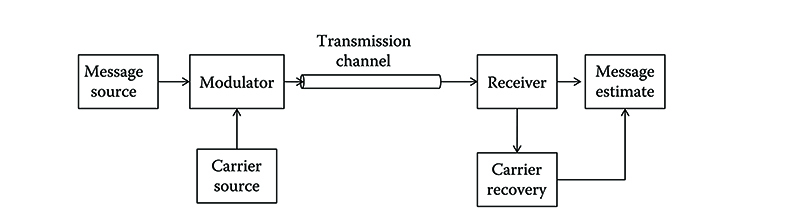
Figure 6.1 Block scheme of a generic single-channel transmission system.
6.2.1.1 Wavelength Division Multiplexing
Whatever design is adopted, the available bandwidth in the third transmission window of optical fibers is so wide that it is not possible to exploit it with a single time division multiplexing (TDM) channel.
Thus, almost all metro and core transmission systems use wavelength division multiplexing (WDM), as shown in Figure 6.2.
At the link near end, several transmitters generate different optical channels using carriers at different frequencies so that they can be multiplexed by an optical multiplexer and sent into the fiber. At the far end, the channels are demultiplexed and processed by an array of optical receivers.
When the optical channels are densely packed in the optical spectrum (e.g., 100 or 50 GHz apart from one another), the multiplexing is called dense WDM (DWDM).
DWDM systems are long-reach and high-capacity systems, require high-quality components, a great design and testing effort, and, therefore, are expensive.
In particular, DWDM transmitters have to be narrowband and frequency stabilized, requiring an accurate temperature control.
The WDM technology can also be adopted designing wide-spaced channels, so that thermal stabilization of transmitters is not needed. These are CWDM systems, designed mainly for application in the metro and access area.
6.2.1.2 Transmission System Performance Indicators
In all transmission systems, noise and other signal distortions are introduced at various points; thus, the extraction of the transmitted symbols from the received signal is a statistical operation prone to errors.
The point-to-point system performance is generally measured by the probability that detection fails in identifying a symbol, which is called symbol error probability. If the alphabet from which the symbols are taken is binary (i.e., there are only two symbols, “1” and “0”), generally this probability is simply called “error probability” or bit error rate (BER).
International standards fix a required error probability that depends on the application, so that systems have to be designed to reach such reference BER [5,6].
In the case of long-haul and ultra-long-haul transmission, the reference BER is 10−12, and we will use this value every time this will be needed.
Frequently, it is interesting to know the degradation introduced in the system performances with respect to an ideal case by a certain phenomenon; for example, what is the degradation introduced by chromatic dispersion?
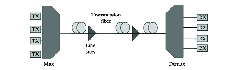
Figure 6.2 Block scheme of a WDM transmission system.
In this case, the degradation is measured through the increment with respect to the ideal case of the received power or of the ratio between the received power and noise (called signal-to-noise [SN] ratio) needed to reach the reference BER: this difference is called penalty.
In a regime of small effect of the nonideal elements, penalties are frequently added together like independent perturbations. This procedure is justified by the assumption that, in a regime of small perturbation, the relation between the BER and the SN ratio does not change and that the dependence of the SN on the perturbation parameters can be linearized.
Let us imagine that in ideal conditions, the BER has the following expression:
BER=e−SNi(6.1)

(6.1)
SNi being the ideal SN ratio both when a 1 is transmitted and when a 0 is transmitted.
Let us also assume that a practical system experiments two impairing phenomena characterized by two parameters A and B (e.g., chromatic dispersion and polarization mode dispersion [PMD]; in this case, the parameters would be D and DPMD).
For a small impact of these phenomena, we can still approximate the BER with (6.1), where the ideal expression SNi is substituted by an expression SN depending on A and B.
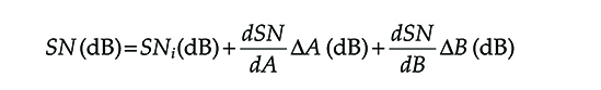
Generally, the logarithmic units are used for the SN ratio; thus, passing from linear to dB and developing at the first order in the small parameters representing the impairing phenomena, we can write
SN(dB)=SNi(dB)+dSNdAΔA(dB)+dSNdBΔB(dB)(6.2)
(6.2)
where ΔA and ΔB are the deviations of the parameter A and B from the values guaranteeing ideal system performances.
If such deviations are sufficiently low, they can be written as
dSNdAΔA≈ΔSN|A(allindB)(6.3)

(6.3)
where ΔSN|A is, expressed in logarithmic units, the variation of SN corresponding to a small variation of A. Thus, Equation 6.2 can be rewritten as
SN(dB)=SNi(dB)+ΔSN|A(dB)+ΔSN|B(dB)(6.4)
![]()
(6.4)
This is the simple rule of penalties addition that says that, for small deviations from the ideal behavior, the SN ratio in dB can be obtained by adding to its ideal value the sum of the penalties relative to all the impairing phenomena, all expressed in dB.
Equation 6.4 is the base for several design techniques, but it has always to be verified in its accuracy due to the approximation used to derive it.
A frequent reason for impossibility to use Equation 6.4 is the fact that the distribution of the noise changes greatly due to the presence of some transmission impairment so that the ideal expression of the error probability cannot be used. In these cases, Equation 6.4 can still be useful if an approximation of the relation between the BER and the SN is known or can be estimated via a suitable simulation.
Phenomena affecting system performances can be random or deterministic in nature. Deterministic phenomena often consist in unwanted distortions of the signal shape, like the effect of fiber nonlinearities or of the nonideal modulator transfer function.
In this case, an intuitive way of quantifying the distortion is the so-called eye opening penalty (EOP). If the receiver samples the signal in the instants tk, indicating with s(t,b) the signal immediately before sampling with its dependence on time and on the transmitted bit b, the EOP is defined as follows:
EOP=10log10si(ti, k,1)−10log10s(tk,1)+10log10s(tk,0)(6.5)

(6.5)
where si(ti,k, 1) is the ideal received signal sampled in the ideal instant ti,k, while the ideal received signal for a zero is considered to be zero.
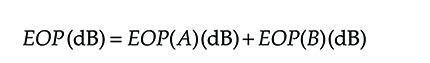
In the presence of random phenomena, like thermal or quantum noise, the EOP is a random variable, and often its average is considered to eliminate the noise and to identify the effect of distortions. In case more distortion effects are present, the EOP can also be expressed in a first approximation as the sum of the EOP relative to each single effect.
The procedure to demonstrate it is similar to that used for the SN and the carrier; it brings to write, in the case of two distortion causes with characteristic parameters A and B, respectively,
EOP(dB)=EOP(A)(dB)+EOP(B)(dB)(6.6)
(6.6)
where EOP(A) and EOP(B) indicate the EOP in the presence of only one of the distorting phenomena.
6.2.2 Ideal IM–DD Transmission
In this very preliminary analysis, we will assume the following simplifying assumptions:
The transmitted message is binary.
The system is point-to-point.
Only one signal propagates along the transmission line.
Information is coded in the signal amplitude.
The fiber transmission is ideal, that is, without dispersion and nonlinear effects.
All transmitter components and all receiver components are ideal; thus, only noise affects the receiver detection.
No optical amplifier is used.
In this condition, the baseband transmitted signal can be written as
s(t)=Σkbkm(t−kT)(bk=0,1)(6.7)

(6.7)
where
m(t) is the pulse that has to shape the transmitted field
T is the period of the transmission: 1 bit transmission will take T seconds
The inverse of this period R = 1/T is called bit rate.
Two possible modulation types exist depending on the shape of m(t): if it is constant in the bit time and zero (or again constant but much smaller) in the adjacent bit times, the modulation is called non-return to zero (NRZ). As a matter of fact, the optical power does not return to zero between the transmission of two consecutive ones and a series of consecutive ones corresponds to a constant signal.
If the pulse m(t) occupies a part of the bit time, leaving a guard time among consecutive pulses so that the signal returns to zero (or to a small value) between two consecutive ones, the modulation is called return to zero (RZ).
Logically, the modulation operation is divided into two steps: the binary message is coded on the electrical carrier (operation that in real systems is done by the remote signal originator) and the obtained current is coded by the modulator onto the CW field emitted by the transmitting laser.
The field is then coupled with the transmission line injecting it in an optical fiber. After coupling loss, the signal at the fiber input contains the information in the slow varying part of the optical field. In telecommunication systems, almost only single-mode fibers are used; thus, the propagating field is also single mode.
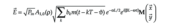
From Equation 4.2, we can write this signal as follows, where the mode transversal shape and the modulation pulses have been considered normalized to one and Pin is the average optical power injected into the fiber in the absence of modulation
→E=√PinA1,0(ρ)√Σkbkm(t−kT)ei[βz−ωt]→x(6.8)

(6.8)
After ideal propagation, the field that arrives in front of the receiver has the following expression:
→E=√PinA1,0(ρ)√Σkbkm(t−kT−)e−αL/2ei[βL−ωτ]M(→x→y)(6.9)
(6.9)
where
L is the fiber length
α is the attenuation
τ is the propagation time
M is the Jones matrix that in the ideal case does not depend on frequency
After detection by the receiving photodiode, the electrical current is proportional to the optical power; thus, in the ideal case in which all the incoming power is detected by the photodiode, the electrical current writes
c(t)=RpPoutΣbkm(t−kT−τ)*H(t)+cbias+ne(t)(6.10)

(6.10)
where
cbias is the detection circuit bias current
Rp is the photodiode sensitivity
Pout = Pine−αL
ne(t) is the detector noise process
H(t) is the pulse response of the electrical front end following the photodiode ∗ represents convolution
In the absence of any optical amplification, the noise is fully due to the sum of two terms: the shot noise and the receiver thermal noise [3]. However, in practical systems without amplifiers, the signal arrives on the photodiode with a great attenuation due to fiber propagation; thus, the shot noise is generally negligible with respect to the thermal noise.
Assuming to have a photodiode based on a internal depletion zone (PIN), in Chapter 4 we have seen that, if the filter H(t) eliminates the low frequency 1/f noise contribution, ne(t) is a band-limited white Gaussian noise whose variance can be indicated with σ2n![]() .
.
At this point, a small part of the signal is baseband filtered so to insulate only the carrier contribution and is sent to a phase lock loop (PLL) that maintains the sampler synchronized with the received signal.
The sampler extracts a sample of the signal (6.10) at the center of the bit interval and compares it with a threshold. If the sample is higher than the threshold, the received bit is assumed to be a one, otherwise a zero.
Calling cth the threshold, two possible receivers do exist: fixed and adaptive threshold receivers.
In the case of fixed threshold, cth is set at the beginning of operation to an optimum value, while in adaptive one it is adapted over times much longer than the bit time to follow slow random fluctuations in the power of the received signals.
If the received signal has a constant average power, the two receivers have the same performances, while this is not true in the presence of intensity noise.
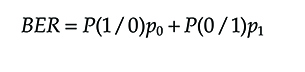
In any case, the BER of our much simplified system is
BER=P(1/0)p0+P(0/1)p1(6.11)
(6.11)
where
p0 and p1 are the probabilities that a zero or a one is transmitted
P(a/a′) is the probability that a is detected when a′ is transmitted
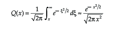
Let us define the Q function as
Q(x)=1√2π∫∞xe−ξ2/2dξ≈e−x2/2√2πx2(6.12)
(6.12)
where the asymptotic approximation holds for high values of x.
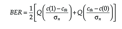
The error probability can be expressed in terms of the Q function like
BER=12[Q(c(1)−cthσn)+Q(cth−c(0)σn)](6.13)
(6.13)
where c(1) and c(0) are the average currents corresponding to the transmission of the two bits.
Equation 6.13 gives the expression of the BER in the very simplified case we have considered up to now, but it is an important reference. The optimum threshold is the value of cth that minimizes the error probability. Deriving Equation 6.13 with respect to cth and equating the derivative to zero it is obtained 2cth = c(1) + c(0) and substituting in Equation (6.13) the BER with the optimum threshold becomes
BER=Q(c(1)−c(0)2σn)=Q(12√SNe)(6.14)
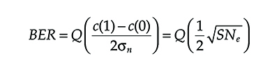
(6.14)
where
σn is the standard deviation of the noise term
SNe indicates the electrical signal to noise ratio
In this ideal system, EOP = c(1) − c(0) so that it is clear why a phenomenon affecting EOP causes a BER reduction.
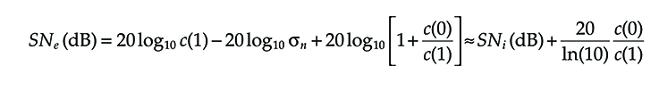
A realistic example of a phenomenon reducing EOP is a limited transmitter signal dynamic range. Ideally, for a given peak power, the BER is maximized for c(0) = 0. In practice, however, the signal zero level is not exactly zero, due to both the inability of the source laser to switch rapidly between the off and the on status and various phenomena like interference with other channels or pulse broadening during propagation that move energy into the bit periods in which a zero is transmitted.
Thus, if the ideal SNe=c2(1)/σ2n![]() in practice, it is SNe=[c(1)−c(0)]2/σ2n
in practice, it is SNe=[c(1)−c(0)]2/σ2n![]() , with c(0)>0
, with c(0)>0
The corresponding optical penalty due to the reduction of the dynamic range can be obtained by passing in logarithmic units so that
SNe(dB)=20log10[c(1)−c(0)]−20log10σn(6.15)
![]()
(6.15)
taking into account that c(1) >> c(0) is needed to assure system working, it can be written
SNe(dB)=20log10c(1)−20log10σn+20log10[1+c(0)c(1)]≈SNi(dB)+20ln(10)c(0)c(1)(6.16)
(6.16)
Thus, the expression of the logarithmic power penalty due to the reduction of the transmitter dynamic range is
ΔSNe(dB)=20ln(10)c(0)c(1)(6.17)
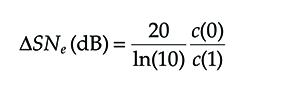
(6.17)
6.2.3 Analysis of a Realistic Single-Channel IM–DD System
The hypotheses that produce Equation 6.14 generally are not fulfilled by a realistic system, due to different reasons.
First of all, transmission through the line is not ideal; dispersion and nonlinear effects generate signal distortion that affects system performances. Moreover, the noise contribution at the receiver is not simply the same Gaussian process whatever bit is transmitted. Different noise processes contribute to the noise and some of them are signal dependent.
In this section, we will start to remove some ideal assumption and to confront ourselves with a realistic system performance evaluation.
In analyzing a realistic IM-DD system we will always assume that the system is functional; thus, all the negative effects have a small impact on system performances and the penalty addition rule can be applied.
6.2.3.1 Evaluation of the BER in the Presence of Channel Memory
In a real system, one of the major phenomenon to take into account is fiber propagation. Due to different effects (e.g., chromatic and polarization dispersion and self phase modulation [SPM]), there is a pulse spreading during propagation, moving energy between adjacent bit intervals.
This effect has a big impact when energy is moved from a “one” to a “zero,” while there is almost no impact if a “one” is adjacent to another “one” or if there is a sequence of “zero.”
This example shows that in a real system the probability that a bit is detected in the wrong way also depends on the nearby bits.
This is called channel memory and has to be taken into account when evaluating system performances.
Under the hypothesis of low distortion, we can limit the analysis to patterns of 3 bits, that we will tag with an index k = 1, 2,…, 8. The bit in a pattern will be indicated with bkj where j = 1, 2, 3 indicates the bit position and k = 1, 2,…, 8 to which pattern the bit belongs.
The eight patterns are
Φ1 = 0 0 0; Φ2 = 1 0 0; Φ3 = 0 0 1; Φ4 = 1 0 1
Φ5 = 1 1 1; Φ6 = 1 1 0; Φ7 = 0 1 1; Φ8 = 0 1 0
Since errors will occur at the receivers, we will distinguish the transmitted pattern, tΦk, whose bits are tbkj and the corresponding pattern estimated at the receiver Φk, whose bits are bkj.
With these definitions, assuming the transmission of uncorrelated and equally probable bits, we have
BER=18Σ8k=1P(bk2≠tbk2|tbk2)=18Σ8k=1Pe(k)(6.18)
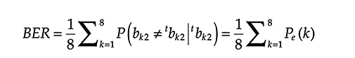
(6.18)
where P(bk2 ≠ tbk2/tbk2) represents the probability to estimate the middle bit of the pattern equal to bk2 when tbk2 was transmitted and bk2 ≠ tbk2.
The BER is evaluated on the middle bit of the pattern since this covers all the possible cases; the other bits of the pattern only serve to correctly represent the channel memory.
6.2.3.2 NRZ Signal after Propagation
In the NRZ case, we will assume the transmitted pulse perfectly squared.
We will assume also that both Raman and Brillouin scattering are negligible. Raman scattering has a high threshold, and we have to avoid a very high power that goes beyond it. As far as Brillouin is concerned, the threshold is quite low and the effect has to be eliminated somehow.
In order to increase the Brillouin threshold, the dependence of the Brillouin gain on the signal bandwidth (see Equation 4.51) is exploited. The spectrum of an amplitude modulated signal can be divided in the sidebands whose width is approximately equal to the bit rate and the central carrier (see Figure 6.3). Since optical systems transmit multigigabit signals, the sidebands’ width is much greater than the Brillouin gain bandwidth and their effect can be neglected with respect to the central carrier.
In general, the central carrier power is above the threshold if effective transmission has to be carried out. However, it is sufficient to operate a direct phase modulation of the transmitting laser (often called dithering and operated by a modulation of the bias current) to increase the carrier spectral width well beyond the Brillouin linewidth ≈ 12 MHz [7].
In this condition the Brillouin gain becomes [8]
GB(ω)=GB0(ω)*S(ω)Ps⇒GB(ωB)≈BBB0GB0(ωB)(6.19)
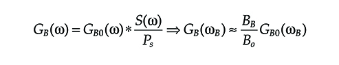
(6.19)
where
BB is the linewidth of the Brillouin gain curve
Bo is the optical bandwidth of the signal pumping the Brillouin scattering
S(ω) is its power spectrum
Ps is its optical power
GB0(ω) is the Brillouin gain for monochromatic pump
ωB is the frequency of the maximum gain
Moreover it is assumed Bo >> BB.
From Equation 6.19 it is derived that a dithering of about 250 MHz causes the Brillouin threshold for an amplitude modulated signal to increase up to about 100 mW. Thus, as far as the transmitted power is below 50 mW Brillouin scattering can be neglected.
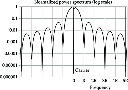
Figure 6.3 Baseband power spectrum of an intensity modulated signal.
Indicating with (→p+,→p−)![]() and (→pi+,→pi−)
and (→pi+,→pi−)![]() the output and the input principal states of polarization (PSPs) of the transmission fiber, the average field at the receiver input can be written as
the output and the input principal states of polarization (PSPs) of the transmission fiber, the average field at the receiver input can be written as
→E=√PinA1,0(ρ)e−αL/2eiβ1Lˆ℘{√Σkbkm(t−kT−τ+)e−iωτ+(→x·→pi+)⇀p++√Σkbkm(t−kT−τ−)e−iωτ−(→x·→pi−)→p−}(6.20)
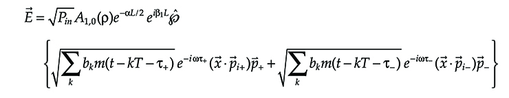
(6.20)
where
ˆ℘![]() is the nonlinear propagation operator
is the nonlinear propagation operator
τ+, τ− are the PSPs’ delays
In compliance with the hypothesis of small nonlinearity, the pulses are assumed to propagate independently so that ˆ℘![]() can be applied to every pulse individually [9].
can be applied to every pulse individually [9].
It is to be noted that not only ˆ℘![]() is nonlinear in general, but also incorporates the channel memory so that it results to be signal dependent. However, this difficulty can be solved by considering the patterns Φk as independent signals instead of the single bits.
is nonlinear in general, but also incorporates the channel memory so that it results to be signal dependent. However, this difficulty can be solved by considering the patterns Φk as independent signals instead of the single bits.
Considering NRZ modulation, if SPM is negligible, the pulse broadening due to chromatic dispersion and PMD can be analyzed separately and added at the end to obtain the overall pulse spread.
Chromatic dispersion effect is deterministic, and can be represented with the effect of a linear operator on the pulses. Due to the channel memory, it is necessary to define eight signals that represents the eight patterns Φk. Calling ηT(t) the function equal to 1 if 0 < t < T and to 0 we can write
sk(t)=3Σj=1bkjηT(t−jT)(6.21)
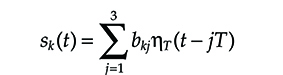
(6.21)
It is noteworthy that sk(t)=√sk(t)![]() so that the signal received when one of the patterns Φk is sent can be rewritten, neglecting SPM and PMD, as
so that the signal received when one of the patterns Φk is sent can be rewritten, neglecting SPM and PMD, as
→E=√PoutA1,0(ρ)eiβ1Lˆ℘DGD{3Σj=1bkjηT(t−τ−jT)}→υ(6.22)
(6.22)
where
Pout is the detected power
ˆ℘DGD![]() represents the dispersion operator
represents the dispersion operator
τ is the average propagation delay
→v![]() is a generic polarization vector
is a generic polarization vector
Now ˆ℘DGD![]() is a well-known operator, and the dispersion related part of Equation 6.22 can be rewritten, passing from the Fourier domain, as
is a well-known operator, and the dispersion related part of Equation 6.22 can be rewritten, passing from the Fourier domain, as
ˆ℘DGD{3Σj=1bkjηT(t−jT)}=T2π3Σj=1bki∞∫−∞sin(ωT)(ωT)eiβ″(ω0)2(ω−ωo)2Ldω(6.23)
(6.23)
The integral can be evaluated numerically via Fast Fourier transform (FFT) to have a correct shape of the received signal for each pattern.
However, a first idea of the broadening of the pulses composing the patterns Φk can be attained much simply by the definition of D itself (see Equation 4.13). In a first approximation the square pulse propagating along the fiber broadens of a factor Δτ = DLΔλ. Naturally, during propagation the pulse shape does not remain squared (as resulting from Equation 6.23), but it is not a great error in regime of small distortion to imagine that the pulse broadens with triangular tails (a comparison between the real pulse shape and a triangular pulse is provided in Figure 6.4, in an extreme case, in which there is strong dispersion distortion).
In this case, just to give an example, in a very first approximation the energy translated from the central “one” to one of the nearby “zero” in the pattern Φ8 = 0 1 0 can be evaluated as E8 = 2PDLRλ2/c where P is the relevant optical power [2]. If we want a rough estimate of the penalty due to pulse broadening in this case, we have to compare the signal power with the interference power which is the energy per unit time. Since E8 is evaluated in the bit interval, this ratio is Pen = E8/PT = 2DLR2λ2/c so that, neglecting the noise, the penalty depends in a first approximation on the square of the bit rate and it is independent from the transmitted power.
If SPM cannot be neglected, the propagation problem cannot be solved analytically and a numerical integration of the propagation equation is needed.
In Figures 6.5 and 6.6 an example of the nonlinear evolution of an NRZ pattern is reported [8] comparing linear evolution (at a transmitted power of −10 dBm) and strongly nonlinear evolution (at a transmitted power of 13 dBm). From the figure, it is clear that the transfer of energy from the “one” to the nearby “zero” is much more pronounced in the linear case, even if the pulse shape is completely distorted in the case of nonlinear propagation. From this qualitative observation, justified by the opposite sign of the phase chirps imposed by chromatic dispersion and SPM, it is intuitive that in opportune conditions SPM can help in attenuating the effects of dispersion.
6.2.3.3 RZ Signal after Propagation
If RZ modulation is concerned exploiting again the hypothesis of small distortions, it is possible to demonstrate [10] that a Gaussian pulse propagating along a fiber remains Gaussian in shape, undergoing a broadening caused by interaction between chromatic dispersion, SPM, and polarization dispersion. While chromatic dispersion and SPM are deterministic phenomena, and their interaction cannot be neglected due to the fact that both produce a chirp that modifies the signal phase, PMD is a statistical phenomenon and the PMD induced broadenings can be considered additive.
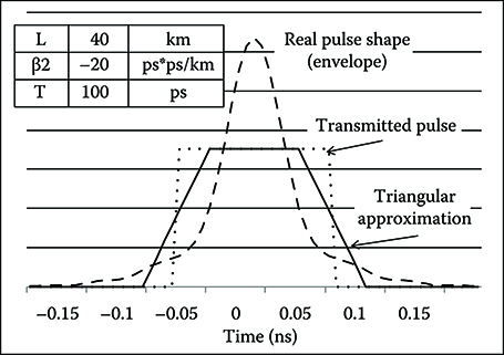
FIGURE 6.4 NRZ pulse after propagating through 40 km of SSMF with perfect linear propagation and absence of PMD. The triangular approximation of the distorted pulse is also shown.

Figure 6.5 NRZ pulse sequence transmitted to generate the example of Figure 6.6.
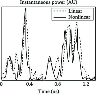
Figure 6.6 An example of the nonlinear evolution of an NRZ pattern comparing linear evolution (at a transmitted power of −10 dBm) and strongly nonlinear evolution (at a transmitted power of 13 dBm). An SSMF fiber is assumed with a length of 30 km.
In [10] the following approximated equation is found for the final pulse width T1 relative to a Gaussian pulse propagating in the presence of chromatic dispersion and SPM:
T1=T0√1+√2LLeLDLNL+(LLD)2[1+43√3(LeLNL)2](6.24)
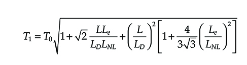
(6.24)
where
L is the link length
Le is defined in Equation 4.36
The dispersion and nonlinear lengths are defined as follows:
LD=T20|β2|LNL=λAe2πn2P0(6.25)
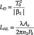
(6.25)
where both the effective area Ae and the nonlinear index n2 are defined in Chapter 4.
Equation 6.64 even if obtained for the first time with a specific derivation, can be derived from the general pulse broadening equation presented in Appendix C.
The expression of the characteristic lengths related to the different phenomena is an important source of intuitive information on the system.
Due to their role in Equation 6.24 and many other equations related to nonlinear propagation in single-mode fibers, they represent the fiber length needed to have a relevant contribution of the considered phenomenon. Thus, longer the characteristic length, the weaker the phenomenon.
The average detected field expression can be rewritten as
→E=√PoutA1,0(ρ)√Σkbkmout(t−kT−τ)e−iφ→υ(6.26)
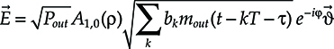
(6.26)
where
Pout is the detected power, taking into account all the attenuation effects
τ is the average propagation delay
φ collects in a single constant all the constant phase terms
→υ![]() is a slowly varying random unitary polarization vector
is a slowly varying random unitary polarization vector
mout is a normalized Gaussian pulse whose width Tout is given by T1 + Δτ, where Δτ is the PMD random delay (compare Equation 4.31)
Equation 6.26 allows us to determine the performance of RZ transmission.
6.2.3.4 Realistic Receiver Noise Model
We have seen that the field emitted by a laser is with an excellent approximation in a coherent quantum state [11]. Narrow band modulation does not change this situation since the coherence time of the modulated field remains very long with respect to the time Tω needed for a complete revolution of the field phase (ωTω = 2π). Thus, the number of photons arriving on the photodiode has a poison statistics and generates the so-called shot noise or quantum noise.
If shot noise is considered, three noise terms appear in the expression of the current: squared shot noise, beat between shot noise and signal, and thermal noise.
6.2.3.4.1 Shot Noise Terms
The shot noise is a signal-dependent noise affecting mainly the transmission of a “one.”
Neglecting the squared shot noise, since it is a second-order term in the noise, and considering that probability p that an incident photon generates an electron is related to the photodiode responsivity Rp by the formula p=ℏωRp/ϵ![]() , where ε is the electron charge, the instantaneous power of the shot noise signal beat is
, where ε is the electron charge, the instantaneous power of the shot noise signal beat is
σ2shot=RpεPoBe(6.27)
![]()
(6.27)
where
Be is the front-end, electrical bandwidth
Po is the instantaneous received optical power
6.2.3.4.2 Detector Noise
The detector noise depends on the photodiode that is used.
Starting from a PIN photodiode, the electrical noise introduced by the photodiode with its front-end signal amplifier depends essentially on the electronic structure of the frontend amplifier (see Chapter 5). Here we will summarize all the parameters of the front end in the so-called noise factor, called Fa, so that we have the following expression for the total noise:
σ2th=4ℜBℑRaFaBe(6.28)
![]()
(6.28)
where Ra is the front-end input resistance. The Boltzmann constant is indicated with ℜB![]() and ℑ
and ℑ![]() is the absolute temperature. In Equation 6.28, the contribution due to the spectral increase of the electronic noise at very low frequencies, the so-called 1/f noise, is neglected. Both for this reason and for coupling reason with the other electronic circuits of the receiver, practical front ends generally exhibit a minimum passband frequency, provided by an input inductive impedance. Below the minimum passband, the electrical signal is eliminated.
is the absolute temperature. In Equation 6.28, the contribution due to the spectral increase of the electronic noise at very low frequencies, the so-called 1/f noise, is neglected. Both for this reason and for coupling reason with the other electronic circuits of the receiver, practical front ends generally exhibit a minimum passband frequency, provided by an input inductive impedance. Below the minimum passband, the electrical signal is eliminated.
A minimum passband frequency around 100 kHz, for example, does affect neither the modulated signal nor the residual carrier (that has to be preserved for the sampling synchronization), and allows low frequency noise to be virtually eliminated.
Besides the thermal noise, practical PIN-based receivers exhibit another form of electrical noise that could give a relevant contribution in specific cases. It is the dark current noise (see Chapter 5) that depends on the fact that, even in the absence of detected radiation, a real PIN photodiode under inverse polarization is traversed by a small current, called dark current, whose amplitude is a random process so that it is seen as another noise source during signal detection.
In case of the use of an avalanche photodiode (APD), besides the thermal noise contribution (Equation 6.28), the APD introduces a so-called excess noise due to the intrinsic random nature of the avalanche gain (see Chapter 5).
The excess noise is generally represented as a sort of shot noise amplification, so that Equation 6.27 can be modified as follows:
σ2shot=2G2mεRpPoFA(6.29)
![]()
(6.29)
where
Gm is the avalanche gain
FA is the excess noise factor, that is a function of the ionization ratio ri (see Chapter 5) and can be written as
FA=riGm+(1−ri)(2−1Gm)(6.30)

(6.30)
Besides multiplication noise, when using an APD, one has to take into account that also the dark current noise is amplified by the avalanche mechanism.
In order to give a correct expression of the amplified dark current noise, one has to take into account that dark current can be divided into two components, depending on the physical phenomenon generating it.
There is a bulk dark current and a surface leakage dark current; the first is really amplified by the APD, the second does not undergo amplification due to the fact that it is a surface phenomenon.
Thus, indicating with Sbd and Ssd the spectral densities of the two components, the final APD dark current power in the detector bandwidth will be
σ2dc=GmSsdBe+G2mSbdFABe(6.31)
![]()
(6.31)
6.2.3.5 Performance Evaluation of an Unrepeated IM-DD System
At this point, we have all the elements to evaluate the BER for an IM-DD system, at least in the hypothesis that the receiver signal processing (i.e., baseband filtering and clock recovery) can be assumed perfect.
Since dispersion involves nearby bits, we need to start from the consideration of the eight pattern of 3 bits that we have called Φk (k = 1, 2, …, 8).
The current corresponding to a certain pattern after detection and front-end amplification can be written as
ck(t)=RpPoutGmΣkbkmk,out(t−jT−τ)*H(t)+cbias+nk,shot(t)+nk,r(t)(6.32)
![]()
(6.32)
where nr(t) collects all the receiver related noise terms: thermal noise, excess thermal noise, and dark current noise and the diode gain Gm has to be set to 1 for a PIN.
Due to the presence of the shot noise term, the statistical distribution of the photocurrent now is not Gaussian. However, as we have noted in the previous section, in the case of the use of a PIN, the thermal noise is largely prevalent in practical systems; thus, it is not a great approximation to consider the noise distribution to be Gaussian.
In the case of an APD, the APD-generated noise can dominate the system performances, but the random behavior of the gain shapes the noise distribution so that a Gaussian approximation is very near to the reality.
Thus, after sampling and bias elimination, the current sample has the following expression:
Ck,j=RpPoutGmbkjmk, out(tk−jT−τ, Δτ)+Nkj(6.33)
![]()
(6.33)
where the noise sample Nkj is the sum of all the noise terms and can be considered a Gaussian variable and the dependence of the sample from the polarization induced delay difference is evidenced.
Once a value of Δτ is fixed, the BER can be evaluated with the technique that was shown in the previous section, only carefully taking into account that the noise variance is dependent on the signal sample.
Thus, the following conditional error probability expressions are obtained, the first for an adaptive threshold receiver, the second for a fixed threshold receiver with the threshold at half the detected signal dynamic range:
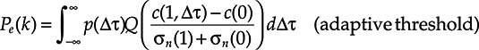
P(erΔτ)=Q(c(1,Δτ)−c(0)σn(1)+σn(0))(adaptive threshold)(6.34)
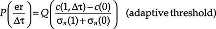
(6.34)
P(er/Δτ)=12[Q(c(1,Δτ)−c(0)2σn(1))+Q(c(1,Δτ)−c(0)2σn(0))](fixed threshold)(6.35)

(6.35)
where “er” represents the error event.
Thus, applying the Bernoulli theorem, the BER is given by
Pe(k)=∫∞−∞p(Δτ)Q(c(1,Δτ)−c(0)σn(1)+σn(0))dΔτ(adaptive threshold)(6.36)
(6.36)
Pe(k)=12∫∞−∞p(Δτ)[Q(c(1,Δτ)−c(0)2σn(1))+Q(c(1,Δτ)−c(0)2σn(0))]dΔτ( fixed threshold)(6.37)

(6.37)
where p(Δτ) is the distribution of Δτ (see Chapter 4).
This technique allows the random effect of the PMD to be incorporated in the evaluation of the error probability.
However, besides the average worsening of the BER, the PMD has also another effect. During the random variation of Δτ short periods can happen where the value of the PMD is very high. In this case the system working is completely destroyed even if for a short period.
The probability of this event called outage is small; therefore, it does not influence greatly the long-term error probability, but when it happens the system could even go down so its importance is beyond the pure influence on the long-term error probability.
This is the reason why generally also the so-called outage probability is evaluated to characterize the PMD influence on a system in situations of high PMD.
We do not detail the evaluation of this parameter in general, encouraging the interested reader to consult [12,13] and Section 9.2.3.2.
6.2.4 Performance of Non-Regenerated NRZ Systems
In order to analyze the effect of all the transmission impairments that are included into Equations 6.36 and 6.37, let us concentrate on the optimum receiver structure: that with the adaptive threshold.
When it will be necessary to evaluate numerical results in this section and in the following, we will use a set of representative parameters reported in Table 6.1, but for fibers’ parameters, that are reported in the Table 4.1 of Chapter 4 for the SSMF and in Table 4.2 of the same chapter for NZ + and NZ –, depending on the fiber type.
TABLE 6.1 Reference System Parameters for the Performance Evaluation Carried Out in the First Part of the Chapter
The first impairment to analyze is chromatic dispersion since in standard single-mode fiber (SSMF) it generates a rapid widening of the transmitted pulses.
To analyze system performances we will require a BER of 10−12 and in agreement with ITU-T recommendations we will evaluate the dispersion limit reach for each system as the distance at which the dispersion induced penalty is 2 dB.
The performance of an NRZ system with no SPM and no PMD, are reported in Figure 6.7.

FIGURE 6.7 Performance of an NRZ system with no SPM and no PMD. System parameters are reported in Table 6.1 but for fibers parameters that are reported in Table 4.2.
As noted in the previous section, pulse broadening has the effect to transfer energy from one bit period to the adjacent one. If this causes energy to be transferred from a one to the adjacent zero, the signal dynamic range is reduced and the BER degrades. This phenomenon is also called intersymbol interference (ISI).
The presence of ISI has a different effect with respect to the noise on the BER curve. Increasing the noise power a greater value of the received power is needed to achieve the same SNe and then the same BER.
However, whatever the required BER, it can be achieved, at least theoretically, transmitting a sufficiently high power.
In the case of ISI, both the energy detected on a “one” and the energy transferred to the adjacent time slots increase proportionally to the transmitted power. Thus, the ratio between the energy that remains in the right time slot and the disturbing energy is constant and no increase of the signal power can change it.
This causes a change of shape of the BER curves and it is expected that the penalty would rise much faster than linear increasing pulse broadening.
The chromatic dispersion penalty can be evaluated from the BER and it is plotted in Figure 6.8 where the foreseen rapid increase of the penalty can be verified.
From the figure, a limit distance of about 36 km is estimated for transmission on SSMF at 10 Gbit/s, while about 132 km are derived for transmission on NZ+.
To understand the penalty trend, when the bit rate changes, in the figure, also a curve relative to 40 Gbit/s on an NZ fiber is shown indicating for this case a dispersion limit of 11 km; thus, the dispersion-limited distance decreases approximately of a factor 16 passing from 10 to 40 Gbit/s.
This is a general trend that can be easily verified using the performance evaluation method detailed in this section: the dispersion limit decreases as the square of the bit rate, at least in a first approximation. This is a confirmation of the rough evaluation carried out in the previous section on the ground of the pulse widening.
It is clear from the aforementioned results that in order to obtain long-reach systems, dispersion has to be compensated.

FIGURE 6.8 Chromatic dispersion penalty for an IM-DD system using NRZ modulation. System parameters are reported in Table 6.1 but for fibers parameters that are reported in the suitable table of Chapter 4.
Several methods have been conceived to compensate dispersion and the most used is the adoption of dispersion compensating fibers (DCFs). It is interesting however to analyze the effect of several different methods.
6.2.4.1 Dispersion-Compensated NRZ IM-DD Systems
Since dispersion is a linear and deterministic phenomenon, in line of principle perfect passive compensation with optical dispersion elements should be possible.
Two kinds of in-line dispersion elements exist: DCF and dispersion compensating gratings.
The DCF can be placed either at the transmitter or at the receiver, even if the receiver position seems advantageous since at the receiver it could be integrated with other devices.
The only real disadvantage in using DCFs is their high loss that in a system without optical amplifiers can be a limitation.
Besides the use of DCF or fiber gratings, electronic compensation or pulse pre-chirp can be used.
The basic idea of the pre-chirp method is to inject into the fiber a signal whose pulses have already a phase modulation exactly opposite to that caused by the fiber dispersion.
During propagation, dispersion compensates this pre-distortion and the pulse arrives at the receiver without any ISI [14–16]. This is a type of pre-distortion similar to that adopted through some electronic devices, but for the fact that it is performed optically.
An important advantage of pre-chirping is that no specific device is needed to apply this technique if an external modulator is used for signal modulation. In this case, pre-chirp can be achieved by simply modulating the transmitting laser bias current or using the pre-chirp embedded functionality that is present in many external modulators.
It is also to be noticed that pre-chirping does not conflict with dithering for Brillouin removal. This last modulation does not have requirements in terms of pulse shape, but only in terms of residual carriers’ bandwidth width.
Pre-chirp has to be optimized for the dispersion of the particular link and generally this optimization is carried out by an automatic control loop driving the chirp parameters in order to maximize either the EOP that is detected at the receiver or, when available through an error correcting code, the estimated BER.
In real systems, the effectiveness of pre-chirp is limited essentially by nonperfect linearity of the phase modulation, by the spurious intensity noise that always comes with a semiconductor laser phase modulation, and by the jitter coming from imperfect synchronization of the phase modulation with the information bearing intensity modulation.
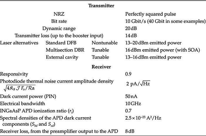
In Figure 6.9, the dispersion related power penalty of a 10 Gbit/s system using a SSMF fiber and optical pre-chirping is shown, evidencing both the effectiveness and the limits of pre-chirping techniques.
An advantage of the use of pre-chirping is that it can be combined with almost all the other dispersion compensating techniques with a good result and that it can be used also in the presence of SPM. Also in this last case, pre-distortion parameters have to be optimized for the specific case.
Another method to compensate for channel distortions is electronic compensation. As discussed in Chapter 5, electronic compensation has two important characteristics: it potentially compensates for every kind of channel distortion, independently from its causes, so that it can be useful also for management of nonlinear effects and, in the case of fast adaptive algorithms, also for PMD. On the other hand, since it is applied on the signal after detection, even if fiber propagation is perfectly linear, the channel as it is viewed by the electronic dispersion compensator (EDC) is a nonlinear channel due to the presence of square law detection carried out by the photodiode.
FIGURE 6.9 Dispersion related power penalty of a 10 Gbit/s system using NRZ modulation a SSMF fiber and pre-chirping technique. System parameters are reported in Table 6.1 but for fibers parameters that are reported in Table 4.1.
(After Boyd, R.W., Nonlinear Optics, Academic Press, San Diego, CA, 2008.)
Since a large number of EDC are digital linear filters, we can expect only a partial compensation.
Of course, this is not true for nonlinear compensation compensator, that in principle can attain much better performances and that, due to the advance in microelectronics technology, is for the first time a practical possibility.
To have an idea of the possible performance of feed forward equalizer–decision driven equalizer (FFE–DFE) compensators, in Figure 6.10 the optical signal to noise ratio SNo needed for a BER of 5 × 10⁻⁴ (i.e., the requirement for systems using a standard forward error correcting code [FEC], see Section 5.8.5.5) is plotted versus distance for propagation over an SSMF and detection using a PIN photodiode [17].
The FFE–DFE compensator allows the dispersion limit (about 36 km in this case without dispersion compensation) to be pushed up to about 70 km in this case, and slightly better results are reported in literature. In the figure also the performances of a Viterbi algorithm–based maximum-likelihood-sequence-estimator (MLSE) compensator are reported. As expected, it is more effective in compensating extra errors coming from signal distortion, pushing the dispersion limit in this case up to about 90 km.

FIGURE 6.10 OSNR needed for a BER of 5 × 10⁻⁴ (i.e., the requirement for systems using FEC, see Section 5.8.5.5) versus distance for propagation over an SSMF and detection using a PIN photodiode of an NRZ IM-DD system using FFE–DFE electronic equalizer at the receiver. Also the performances of a Viterbi algorithm-based MLSE compensator are reported. System parameters are reported in Table 6.1 but for fibers parameters that are reported in Table 4.1. (After Xia, C. and Rosenkranz, W., IEEE Photon. Tech. Lett., 19(13), 1041, 2007.)
As discussed in Section 5.8.3.1, Viterbi algorithm changes the statistics of errors after the compensator; thus, the effect of the FEC cannot be evaluated assuming independent errors. Several studies are ongoing to determine exactly the impact of this element and to find an optimum design for the overall MLSE + FEC system, and probably this difficulty will be soon overcome with a global design taking into account both the elements together.
Even more effective results can be obtained using pre-distortion of the transmitted signal through a look-up table designed to compensate both linear and nonlinear signal distortions.
This method is not easy to implement and to control during system working, but it is very high performing, as it is demonstrated, for example, in [18]. The performance of a mix look-up table and linear electronics equalizer are reported in Figure 6.11 [18], where a maximum distance of more than 500 km is foreseen with only signal pre-distortion in pure linear propagation.
Let us now assume that chromatic dispersion has been completely canceled. In this case limitations arise to the transmission reach from PMD and SPM.
Let us start to assume transmission at low power, so that SPM is negligible, and to operate with a fiber installed before the discovery of the importance of controlling the PMD (a lot of fiber installed before the years 2000 are manufactured with processes that can produce a high PMD).
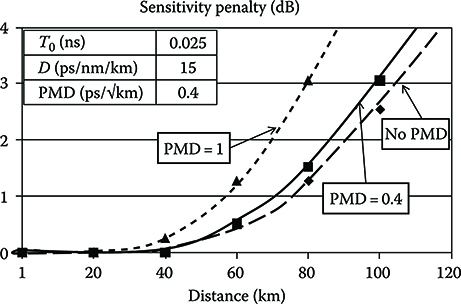
Thus, let us assume the parameters of an SSMF fiber with a residue chromatic dispersion after compensation of 0.5 ps2/km and a PMD parameter of 0.4 ps/km1/2.
The PMD induced penalty is shown in Figure 6.12 versus distance for 40 and 100 Gbit/s. It is clear that great areas of the figure do not correspond to links that can be realized with unamplified systems, but the graphic is quite important since, due to the linear nature of PMD, the effect is independent of the transmitted power. This means that Figure 6.12 approximately holds also for amplified systems (but for the fact that an accurate estimation of the penalty in that case has to take into account the different noise distribution).
Figure 6.12 demonstrates that PMD is an important impairment in long-reach, high bit rate systems, and in a few important cases, for example, when mixed erbium-doped optical fiber amplifier (EDFA)–Raman amplification is used to maintain the optical power low and avoid nonlinear effects, it can be the ultimate limit to the system reach.
FIGURE 6.11 Performance of a mix look-up table and linear electronic equalizer: a maximum distance of more than 500 km is foreseen with only signal pre-distortion in pure linear propagation. System parameters are reported in Table 6.1 but for fibers parameters that are reported in Table 4.1.
(After Killey, R.I. et al., IEEE Photon. Tech. Lett. 17(3), 714, 2005.)

FIGURE 6.12 PMD induced penalty versus distance for 40 and 100 Gbit/s. The parameters of an SSMF fiber with a residue chromatic dispersion after compensation of 0.5 ps2/km and a PMD parameter of 0.4 ps/km1/2 are considered. The system parameters are reported in Table 6.1.
PMD compensation is much harder with respect to chromatic dispersion compensation due to the fact that PMD not only is time varying, but it is also a random process. This means that the only possible way for compensation is to devise an adaptive compensator.
For their nature, all electronics adaptive dispersion compensators can be optimized so to face also PMD. The great majority of them does not distinguish pulse broadenings due to different physical causes so that, naturally, they try to compensate any distortion.
However, linear compensators like FFE–DFE suffer in terms of performances of the nonlinear nature of the communication channel.
Completely different is the situation for adaptive nonlinear compensator that reaches a very good level of compensation (see Figure 6.11).
Up to now, we have evidenced the penalty caused by linear and nonlinear propagation effects on the system performances.
Now we pass to consider another important element of the transmission chain: the detector. A PIN photodiode can be substituted with an APD, so to exploit the detector gain to increase the SNe that is dominated by the receiver thermal noise.
From the previous section, we have all the elements to analytically estimate the BER in this case. There is only one important observation to do.
Looking at Equations 6.27 through 6.29 we can see that the overall noise power is composed of two terms. The thermal noise that does not depend on the APD gain and the sum of shot noise and dark current noise that depends on the gain.
For a great value of Gm the shot term prevails and increasing the gain the SNe decreases; for small values of Gm the APD behaves like a PIN with a small gain so that increasing the gain the SNe increases.
This behavior indicates the presence of an optimum gain that maximizes the SNe. The optimum gain naturally depends on the parameters of the APD. Just for an example, the parameters of a medium performance InGaAs APDs are reported in Table 6.1. The optimum gain at 10 Gbit/s is around 28. In Figure 6.13 the sensitivity (input optical power needed to attain a BER of 10−12) is shown versus the APD gain in the absence of dispersion and nonlinearity.

FIGURE 6.13 Sensitivity (input optical power needed to attain a BER of 10−12 at 10 Gbit/s) versus APD gain in the absence of dispersion and nonlinearity. The parameters are reported in Table 6.1.
In this ideal condition, the sensitivity gain due to the APD is around 9 dB, passing from a PIN sensitivity of about −24.5 dBm to an APD sensitivity of about −33.5 dBm.
The impact of the other performance decreasing factors on APD receivers are not different from what we have seen in the case of the PIN receiver, but for the sensitivity gain.
The only factor that is sensibly impacted from the presence of an APD is the role of SPM. As a matter of fact, for a fixed fiber link, the presence of an APD at the receiver allows the optical power to be maintained much lower, so reducing the effect of SPM.
6.2.5 Performance of Non-Regenerated Return to Zero Systems
Considering RZ systems, the performances in condition of ideal propagation are the same with respect to NRZ, since they depend only on the signal and noise energy received in the bit interval.
The situation is completely different in the case of presence of dispersion. In the case of chromatic dispersion, two things happen when decreasing the pulse width.
On one side, the dispersion is more efficient, the relative pulse broadening being bigger, on the other side, the pulse does not occupy the whole bit interval; thus, some broadening can be accepted if no energy is transferred in the nearby intervals.
As usual, when two different phenomena tend to balance we have to expect an optimum value of the pulse width at which the penalty due to chromatic dispersion is minimum.
As we have mentioned in Chapter 4, the pulse propagation problem in the presence of chromatic dispersion can be solved exactly in the case of Gaussian pulse. In this case, it is possible to derive the following expression of the output pulse root square medium width (that is also half the width at 1/e below the maximum), obtaining [2]
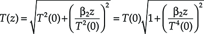
T(z)=√T2(0)+(β2zT2(0))2=T(0)√1+(β2zT4(0))2(6.38)
(6.38)
that is Equation 6.17 in the limit of LNL → ∞. This expression is another example of the more general rule to analyze the widening of a pulse traveling through a cascade of filters that is derived in Appendix D. As a matter of fact, the factor that is added to the unit under the square root is exactly the square of the width of an ideal filter that has on the optical pulse the same effect of the dispersion.
Thus, ΔT = T(z) − T(0) is minimum at a distance L from the transmitter, if T(0)=√β2L![]() . For an SSMF this means, at a distance of 40 km, T(0) = 0.028 ns that is a short pulse with respect to the duration of 0.1 ns of the bit interval at 10 Gbit/s, but it is not sufficiently short for 100 Gbit/s transmission, where the bit interval is 0.001 ns.
. For an SSMF this means, at a distance of 40 km, T(0) = 0.028 ns that is a short pulse with respect to the duration of 0.1 ns of the bit interval at 10 Gbit/s, but it is not sufficiently short for 100 Gbit/s transmission, where the bit interval is 0.001 ns.
Moreover, increasing the distance the optimum pulse becomes longer. This can be understood by observing that, for very large distances, the term containing dispersion is so high that the other term under square root can be neglected and the final pulse width is inversely proportional to the square of the initial width so that shorter launched pulses produce longer output pulses.
For example, at 10 Gbit/s and with β2 = 20 ps2/km, the optimum pulse at 300 km is 77 ps. Since this is the half width at 1/e, this means that we are quite near NRZ, with a pulse whose real width is 50% wider than the bit interval (if a real transmission would be set up, naturally only the part of the pulse within the bit interval would be transmitted).
In the following analysis of 10 Gbit/s systems, we will consider practical pulses never shorter than 10 ps and never longer than half the bit interval whatever the distance and the bit rate.
In order to define the pulse width we will use the so-called duty cycle of the RZ modulation that is defined as (2T0R) so to be in practical cases always smaller than one so to be measured in percentage unit. In a 10 Gbit/s RZ modulation with a duty cycle of 30% the full width at 1/e of the used pulses is 30 ps out of the 100 ps of the bit interval.
The sensitivity penalty of an unrepeated and uncompensated RZ system using pulses of 25 ps is shown in Figure 6.14 for propagation on an SSMF and different values of the PMD parameter. The effect of PMD is evident also at short distances due to the short pulses.
For uncompensated systems on high dispersion fibers, some working zones can be individuates, where there is a partial compensation between the chromatic dispersion and the SPM induced chirps. Although this phenomenon is not particularly useful in unrepeated system, it is important as the base on which the design of nonlinear aided WDM system is founded [8].
6.2.6 Unrepeated Wavelength Division Multiplexing Systems
The huge bandwidth available in the third transmission window of optical fibers naturally move the interest toward frequency multiplexing, that in the field of optical transmissions is called WDM.
In general, WDM systems are called DWDM if the channels are a few GHz far, one from the other. Typical channels’ spacing for DWDM systems at 10 Gbit/s are 50 or 100 GHz, while for 40 Gbit/s a typical spacing is 200 GHz.
DWDM systems require frequency stabilized sources and suffers sizeable interference among adjacent channels due to different phenomena.
Differently, CWDM (coarse WDM) systems have 20 nm spaced channels, so that up to 18 channels can be used in the low attenuation bandwidth of an optical fiber, if the water absorption peak is not present (compare Chapter 4).
The 20nm spacing is chosen on the ground of the standard characteristics of semiconductor lasers, so to be able to use uncooled sources to reduce the system cost.
CWDM systems are mainly used in the metro and metro access area, where distances are not so long and the cost is a key issue.
In addition to phenomena impacting the single channel, channel crosstalk is another relevant degradation source in WDM systems.
Assuming an NRZ signal, the received field can be written as follows:
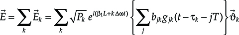
→E=Σk→Ek=Σk√Pkei(β1L+kΔωt){Σjbjkgjk(t−τk−jT)}→υk(6.39)
(6.39)
here k is the channel index that is assumed to run from −N/2 to N/2 being N + 1 the channel number. Since the channels interact one with the other, the received pulse in the jth bit interval, not only depends on its position in the bit stream, but also on the considered channel; this is the reason why the pulse g jk(t) has both the channel index k and the slot index j. The channels will be asynchronous in time, since their group velocity is different, so that the propagation delay τk brings the channel index.
Similarly to the delay, the polarization also will be different from channel to channel, justifying the channel index on the polarization unitary vector →υk![]() .
.
Last but not least, the detected power also depends on the considered channel, due to the nonuniform wavelength response of optical components, and it is labeled as Pk.
In the usual hypothesis that the transmission impairments are small and can be treated as perturbation of the ideal system, we will go on analyzing the interference in form of a power penalty, to add to penalties coming from other sources.
Two kinds of interferences are potentially present in WDM systems: linear and nonlinear interference.
The term linear and nonlinear depends on the fact that the first type is always present, even when linear propagation can be assumed, while the second is related to nonlinear fiber propagation.
6.2.6.1 Linear Interference in Wavelength Division Multiplexing Systems
Linear interference arises due to the fact that there is an overlap between adjacent channel optical spectra, so that the power of a channel unavoidably interferes with the adjacent ones, as shown in Figure 6.15.
This effect has to be limited by optical filtering, since after quadratic detection, all the channel spectra superimpose in the electrical baseband. Indicating with Ho(t) the optical pulse response of the optical filter, the electrical field relative to channel k = 0 after demultiplexing and, if needed, further optical filtering is given by
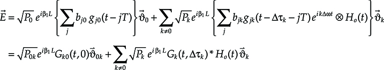
→E=√P0eiβ1L{Σjbj0gj0(t−jT)}→υ0+Σk≠0√PkeiβiL{Σjbjkgjk(t−Δτk−jT)eikΔωt⊗H0(t)}→υk=√Pokeiβ1LGk0(t,0)→υ0k+Σk≠0√Pkeiβ1LGk(t,Δτk)*H0(t)→υk(6.40)
(6.40)
where Gk(t,τ) represents the signal conveyed by the kth channel, whose expression can be easily deduced from Equation 6.33, in a first approximation the filtering effect of Ho(t) on the selected channel is neglected and Δτk = τk − τ0.
Generally, for a well designed WDM system, only adjacent channels generate relevant linear interference; thus, the index k in Equation 6.40 can assume only the values −1 and 1.
From Equation 6.40, the current after detection can be derived obtaining in the jth time slot:
cj(t)=RpP0Gj(t,0)+RpΣk≠0√Pk0PkGj0(t,0)Gkj(t,Δτ)⊗H0(t)→υk·→υ0+Σk≠0RpPkGkj(t,Δτ)+n(t)(6.41)
![]()
(6.41)
where n(t) represents the global noise term, and a PIN receiver is assumed.
From Figure 6.15 it is clear that the part of the spectrum of an adjacent channel entering the selection filter has to be small. In this condition, the 0–j beat term is quite bigger with respect to the j–j so that this last term can be neglected.

FIGURE 6.15 Linear interference due to the overlap between adjacent channel optical spectra.
Even with this simplification, the analysis of the linear interference impact is difficult due to the random nature of this effect. As a matter of fact, both the scalar product of the polarization vectors and the relative delay are slowly varying random variables.
However, due to the slow variation, calculating their distribution and the related average BER can be misleading. As a matter of fact, the random variables related to polarization and delay can assume, for a long time, values near the worst case, thus heavily influencing the transmission of many bits.
For these reasons, it makes sense to evaluate the worst case BER penalty.
The worst situation is obtained when interfering channels carrying a “one” signal are synchronous and co polarized with the useful channel (see Equation 6.41) [19].
With all these approximations the photocurrent writes
Cj(t)=RpP0Gj(t,0)+RpΣk≠0√Pk0PkGj0(t,0)Gkj(t,0)⊗H0(t)+n(t)(6.42)
![]()
(6.42)
and we can use the tools used in the previous sections to evaluate the BER.
In Figure 6.16, the worst case linear interference penalty is plotted versus the channel spacing at 10 Gbit/s and for different optical filters. Perfect dispersion compensation and absence of relevant PMD and SPM are assumed. The results are plotted searching the worst case with respect to the relative phase of the carrier of the considered and the interfering channel. This assumption is important for small channel spacing, where only few oscillations of the relative interfering carrier (with angular frequencies Δω) are comprised into the bit interval. In normal situations, where there is at least a factor 5 between the bit interval and the interfering carrier relative frequency this is not an important assumption.
Gaussian filters are considered in Figure 6.16a while ideally rectangular filters are used to plot Figure 6.16b.
Moreover, the optical bandwidth is unilateral and this convention will be always assumed in this book. Thus, the minimum optical bandwidth that catch the entire signal spectrum main lobe is Bo = R and the Nyquist bandwidth is Bo = R/2.
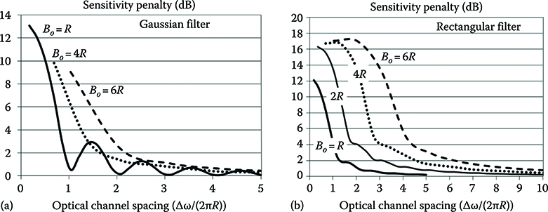
FIGURE 6.16 Worst case linear interference penalty versus the channel spacing for different optical filters: (a) shows the results for Gaussian filters (where the bandwidth is half width at 1/e) and (b) for rectangular filters.
The impact of the optical filter shape is clear, since the amount of interference power depends on the filter shape.
From the figures, also the oscillating nature of the interference can be noted, that depends on the channels spectrum shape.
6.2.6.2 Nonlinear Interference in Wavelength Division Multiplexing Systems
Nonlinear interference depends on nonlinear fiber propagation. The effects that give the main contribution to this interference term are Kerr induced four wave mixing (FWM) and Kerr induced cross phase modulation (XPM), assuming as always that the Brillouin effect is neutralized with a sufficiently fast source dithering [10].
Equations 4.45 and 4.46 allow us to evaluate the FWM power on the various frequencies arising due to this effect. The main hypothesis here is that the channels can be considered monochromatic, that means the bit rate R is much smaller than the channel spacing.
This condition is verified several times, but not always. For example, it is not verified in the case of a DWDM system at 10 Gbit/s and a channel spacing of 25 GHz.
Fortunately, in the case of 10 Gbit/s systems with 100 or 50 GHz spacing, the monochromatic channel assumption is quite reasonable.
In principle, knowing the FWM power hitting the signal bandwidth does not allow a complete performance evaluation.
As a matter of fact, the FWM instantaneous power in a signal bandwidth fluctuates with time due to the channels modulation, walk-off, and polarization changes. The channel walk-off is due to the fact that different channels have different group velocities; thus, the alignment of the transmitted bit streams varies with time while one “slides” with respect to the other. Since an FWM term arises only when a “one” is transmitted on all the involved channels, walk-off causes the FWM power to change in time.
A similar variation is due to polarization fluctuations. Since we have seen in Chapter 4 that the bandwidth of the PSP is about 100 GHz, if the channel spacing is on the order of 100 GHz or greater, the polarization of different channels evolves independently. FWM happens only when the polarization of the involved channels is almost the same; thus, polarization fluctuations cause FWM power to change in time.
These FWM fluctuations have fast and slow components (as fast as twice the bit rate and as slow as polarization fluctuations) and their exact statistic is complex. In the realistic case, in which there are many WDM channels, several contributions are added on the same wavelength and in a first approximation the FWM can be considered a sort of narrowband colored Gaussian noise [2,8].
Once this approximation is made, the system performance in the presence of FWM can be evaluated by considering a central channel of the WDM comb (i.e., the channel in the worst situation regarding FWM products) and evaluating the number of products contained in the channel bandwidth and the overall FWM power as the sum of their individual powers [20].
As an example in Figure 6.17 [21], a system with nine channels, 30 km long and without dispersion compensation is considered. The transmitted power is 0 dBm per channel. In the figure, the power penalty due to FWM is shown versus the channel spacing.
The first thing to notice is the oscillatory behavior of the curves. This is due to the oscillatory behavior of the phase matching term and also the fact that only the main FWM terms are accounted for in the figure. Considering all the terms the oscillation results less deep in correspondence of the points in which the main terms nullify.
FIGURE 6.17 FWM power penalty versus channel spacing for a system with nine channels 30 km long without dispersion compensation. The other system parameters are reported in Table 6.1.
In designing a WDM system, it is not possible to exploit the fact that the FWM power is strongly reduced around some points for the aforementioned fluctuations of the phase matching conditions, and it is necessary to evaluate the FWM penalty using the envelope of the maximum values of the curve of Figure 6.17.
The strong effect of fiber dispersion is also evident from Figure 6.17, where the FWM impairments are much more severe in the case of an NZ fiber.
Last but not least, the impairment due to FWM has a step behavior typical of nonlinear phenomena. On this ground, an FWM induced capacity limit can be introduced, that is the limit to the product distance by bit rate imposed by the FWM effect.
In general, this is defined as the point on the envelope of the maxima of a figure similar to Figure 6.17 at which the FWM causes a penalty of 1 dB.
This limit can be evaluated starting from the FWM total power as follows. Let us define the FWM to noise ratio FN as the ratio between the FWM power and the optical noise power in the optical selection filter bandwidth: FN = Pf/σo.
If we consider a system limited by the optical noise (that is the most interesting case) and we assume the FWM power as an additional optical noise source, it results
SN0=P0Pf+σ0(6.43)

(6.43)
Then, since ideal SNo is given by SNi = Po/σo the FWM induced penalty can be written as
PenFWM=SN0SNi=FN+1(6.44)
![]()
(6.44)
The analysis of the XPM is a bit more complicated due to the fact that the expression of the XPM induced crosstalk power has to be carried out by dealing with the nonlinear propagation equation in a more complicated way with respect to FWM.
This study is carried out in detail in [22] while a simple but sufficiently accurate model in almost all the practical cases is reported in [23]. We will use this last model, since all the WDM designs we will do will always be verified by simulation.
The conclusion of the model presented in [23] is that also XPM can be considered like a power dependent noise due to the combined effect of modulation, walk-off, and polarization fluctuations.
In analogy with FWM, an XPM to optical noise ratio can be defined XN = Px/σo, where Px is the XPM equivalent noise power so that, the XPM induced penalty can be written as
PenXPM=XN+1(6.45)
![]()
(6.45)
The XPM power affecting the kth channel of the WDM comb can be evaluated by the following equation
Px=4γ2〈P〉2NΣj=1j≠k∞∫−∞Sj(ω)|Hj,k(ω)|2dω(6.46)
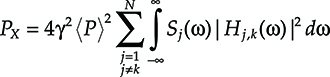
(6.46)
where
k is the index of the selected channel
〈P〉![]() is the average optical power
is the average optical power
Sj(ω) is the interfering channel normalized power spectral density so that ∫∞−∞Sj(ω)ⅆω=1![]()
Hj,k(ω) is the representation of the interaction between the jth and the kth channels and it is given by
Hj,k(ω)=i{1−e[−αL+i(δj,kω−Ψω2)L]α−i(δj,kω−Ψω2)−1−e[−αL+i(δj,kω+Ψω2)L]α−i(δj,kω+Ψω2)}(6.47)

(6.47)
where
α is the attenuation in m−1
δj,k is the so-called walk-off factor, that is the inverse of the difference between the group velocities of the considered channels
Ψ is related to the fiber dispersion by the equation Ψ = Dλ2/4πc, λ being the central wavelength of the WDM comb and c the light speed in glass
L is the length of the link
Equation 6.46 has to be integrated numerically, but it is much easier than a simulation. We will use several times this approach for its simplicity.
6.2.6.3 Jitter, Unperfected Modulation, Laser Linewidth, and Other Impairments
Besides the phenomena we have dealt in the previous sections, there are several other potential performance impairments that have to be considered when evaluating the performance of an optical transmission system.
These effects are not so important as dispersion or FWM, but if not managed with a correct system design they can heavily affect system performances.
Timing jitter: This phenomenon consists of the fluctuations of the receiver decision circuit sampling instant. It is intuitive that, if sampling does not occur at the center of the bit interval, a penalty is generated. Timing jitter generally depends on the imperfect working of the receiver PLL, causing the reconstructed clock to be affected by phase fluctuations. A correct design of the digital receiver PLL can make this phenomenon negligible [24].
Pulse jitter: This phenomenon, affecting mainly RZ transmission, consists in the fact that the transmitted pulses are not located exactly at the center of the bit interval. The cause can be phase noise in the clock at the transmitter, a random component in the switch-on or switch-off time of the transmitting modulator, or even pulse attraction due to nonlinear propagation for quasi-soliton RZ pulses when very long, amplified systems are considered. Transmitted pulses’ position fluctuations cause ISI and have to be carefully controlled during system design [25].
Limited transmitter dynamic range: In this case the difference between the “one” level and the “zero” level is not sufficient to assure correct system working. This effect can be due to a wrong drive of the modulator or by the use of a modulator with unsuitable characteristics. Since a limited dynamic range reflects in a proportional increase of the EOP this has to be specified with great attention before accepting a certain transmitter in the system design.
Transmitting laser linewidth: Even if semiconductor lasers are high performing and very stable sources, nevertheless, they have a finite linewidth due to homogeneous broadening of the emitted mode. Generally, lasers used for DWDM transmission have a linewidth on the order of 1 MHz or less and the impact on system performances is negligible. However, if the linewidth should increase it can disturb the receiver PLL causing timing jitter [2].
Polarization dependent losses: Imperfect connectors positioning or other problems along the line (like transit through patch panels in the metro area) can cause polarization depending losses (PDL). PDL also affects the system performances increasing effective losses and creating unbalance between the output polarization principal states.
Excess losses due to passive optics: In a realistic DWDM system there is a lot of passive optics (like connectors, patchcords, etc.) to bring the signal from one card to the other. All these elements introduce losses that can be important in case of bad mounting or of a damaged connector.
Amplifiers gain curve ripple: Although gain flattening filters are usually adopted in optical amplifiers to smooth the gain curve, cascading several amplifiers could evidence also small imperfections. If a channel gain is globally greater it can depress the gain of nearby channels creating a relevant penalty.
6.3 Intensity Modulation and Direct Detection Systems Using Optical Amplifiers
In the previous section, we have analyzed optical transmission systems without optical amplifiers. Even if all the transmission impairments are somehow managed, the fiber attenuation and the receiver sensitivity set a limit to the product bit rate–distance that can be assumed as a sort of system quality factor.
With an APD receiver having a sensitivity of −34 dBm at 10 Gbit/s and a transmitter that injects about 1 dBm in the fiber, the pure power budget limits the transmission to a distance of 140 km due to the fiber attenuation assumed to be 0.25 dB/km.
Using optical amplifiers to boost the signal along the line this limit is completely removed. Not only the amplifier compensates for the fiber loss, but allows transmitting less power, thus limiting nonlinear effects.
Almost all the practical transmission systems that are on the market use optical amplifiers; thus, there is a wide variety of amplified systems depending on the application.
Here we will divide the systems in three categories:
Long-haul and ultra-long-haul systems are characterized by an amplifier chain constituting the transmission line; they can use any type of amplifier, depending on the needs, and their reach exceeds several thousand kilometers
Single span systems use only booster and preamplifiers and generally they are mixed EDFA–Raman amplifiers. They are used for applications in which the distances are not so big
Optical ring, characterized by the ring topology, they are used mainly in the metropolitan network
6.3.1 Long-Haul and Ultra-Long-Haul Transmission: Performance Evaluation
The principle scheme of the simpler long-haul DWDM system is shown in Figure 6.18. After the transmitter, a preamplifier brings the power to the desired level at the transmitter; the line is divided into spans and at each span end another amplifier is present. Since, due to the long reach of these systems, dispersion has to be compensated by some in-line device, in-line amplifiers will have the possibility to insert between the amplification stages a loss. This loss will be generally caused by a DCF, even if more complex situations arise when dynamic devices as some optical add drop multiplexers (OADMs) are used.
Thus, at the end both loss and dispersion are compensated, respectively, by optical amplifiers and DCFs.
Now we will apply all the methods introduced in the last sections to assess the performances of the system sketched in Figure 6.18 when EDFA amplifiers are used.
The noise contribution at the receiver will be mainly caused by amplifiers amplified spontaneous emission (ASE) accumulation, since the presence of a preamplifier will make the received signal quite more powerful than in unamplified cases. Moreover, a PIN is generally used at the receiver since further amplification after the preamplifier is not needed.
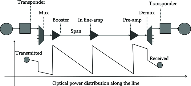
FIGURE 6.18 Block scheme of a long-haul DWDM system and optical power distribution along the line.
In order to determine the electrical noise, let us consider the transmission line like a cascade of amplifying and attenuating elements. In this simple model, let us imagine that all the in-line amplifiers are equal and that the net gain resulting from the two stages and the attenuation due to the interstage loss exactly compensate the loss of one span.
In real systems, the amplifiers are generally hosted in preexisting locations where the carrier has a point of presence. These locations could not be at the same distance, one from the other; thus, a more complicated situation arises. We will evaluate later the characteristics of a chain of amplifiers that are not at the same distance.
A single double stage amplifier with an interstage loss has a noise figure NFtotal = NF1 + NF2/(αG1) (compare Section 4.3.1.4) and it is optimized so to minimize the overall noise figure for the considered loss. Thus, we will assume that all the in-line amplifiers are optimized for the correct value of the DCF loss and have a noise figure equal to NFil.
The system will have also a booster at the transmitter that we will assume a single-stage amplifier optimized to perform as booster and at the receiver a preamplifier will be present. The booster and preamplifiers noise figures will be NFb and NFP, respectively.
To provide an example of numeric performance evaluation, we will assume that the transmission fiber is an SSMF and that the values of the various system parameters are those reported in Table 6.2.
An exact evaluation of the noise at the amplifier chain is complex due to the fact that the electromagnetic field propagating in a generic system span is not in a minimum energy state due to the ASE contribution of the previous amplifiers [11]. The result of the exact quantum mechanical evaluation of the overall noise is reported in [19]. However, in a realistic telecommunication case, amplifiers are low-noise high-gain components, so that the only noise term that is relevant after detection among the noise processes caused by the amplifier chain is the so-called beat noise, that is the beat between the signal and the accumulated ASE.
TABLE 6.2 Parameters for the Design Examples of DWDM Amplified Systems

In this hypothesis, every amplifier introduces an optical noise whose power is given by
σj=ℏωBoGjNFj(j=1,...,Na)(6.48)
![]()
(6.48)
where Bo is the unilateral optical bandwidth.
Here it is necessary to remember the convention we have already introduced in Chapter 5 to evaluate the noise power of amplified systems.
We define a unilateral power spectral density as Sω=ℏωcGNF![]() where ωc is the carrier angular frequency. Since the noise factor is involved in the expression of the noise power spectral density instead of the population inversion, the noise power is obtained by multiplying it by the unilateral optical bandwidth Bo. If the signal spectrum is mainly contained in the angular frequency interval (ωc − ωM; ωc + ωM) and in the symmetric on the negative ω axis, Bo is defined as Bo = ωM/2π.
where ωc is the carrier angular frequency. Since the noise factor is involved in the expression of the noise power spectral density instead of the population inversion, the noise power is obtained by multiplying it by the unilateral optical bandwidth Bo. If the signal spectrum is mainly contained in the angular frequency interval (ωc − ωM; ωc + ωM) and in the symmetric on the negative ω axis, Bo is defined as Bo = ωM/2π.
The signal at the end of the chain can be written as
→E=NcΣk=1Ek(t)eiωkt→υk+Na+2Σj=1nj(t)→ξj(6.49)

(6.49)
where
Na is the in-line amplifiers’ number so that the overall number of amplifiers is Na+2 →υk![]() and →ξj
and →ξj![]() represent casual polarization vectors
represent casual polarization vectors
The transmitted field intensity Ek(t) contains the information. The indexes j and v run over the number Na of amplifiers and the index k over the number Nc of WDM channels.
Due to the hypothesis that every amplifier compensates exactly the loss of the previous span, we can set
NaΠj=1Gje−αLj=j−1Πv=1Gve−αLv=1(6.50)
(6.50)
thus greatly simplifying expression (6.49). Moreover, from the consideration that all the ASE processes are independent since they come from different amplifiers, it results that the noise power is simply the sum of the ASE noise powers generated by each amplifier of the chain and the same holds for the overall noise figure, so that
NFTOT=Na+2Σj=1NFj=NFb+NFb+NaNFil(6.51)
(6.51)
Starting from Equation 6.51, it is possible to optimize the amplifiers span, that is, to set the optimum value of Na once given the amplifier noise characteristics and the link length L.
To do that, it is necessary to fix the bonds under which the optimization has to be performed. If amplifiers are used, periodically the signal returns to a high power level; thus, different from the case of unamplified systems, nonlinear effects happen over a long part of the link.
If the link has to work it is needed to limit the average power below a threshold, so to be sure that nonlinear effects remain under control. Since no solution in which the average power is higher than the threshold is acceptable, it is reasonable to optimize the overall link by maintaining constant the average power.
If this is the optimization bond it is useful to introduce in Equation 6.51 a different expression of the amplifiers number Na.
From the equation ∏Naj=1Gje−αLj=GNaile−NaαLs![]() where Ls is the span length, the following expression of Na can be derived:
where Ls is the span length, the following expression of Na can be derived:
Na=αLsln(Gil)(6.52)
![]()
(6.52)
Substituting this expression of the number of amplifiers into the expression of the noise power generated by the line and using the noise factor to evaluate the overall ASE spectrum SASE is obtained
SASE={αLsln(Gil)(Gil−1)NFil+(Gp−1)NFp+(Gb−1)NFb}ℏω(6.53)

(6.53)
Since the average power in fiber and the bit rate are fixed, the SNo and, thus, the error probability is optimized, if SASE is minimized. In order to minimize SASE, it is necessary to decrease Ls up to the limit of continuous amplification. In this limit, the amplifiers’ gain is very small (tends to zero in the absence of DCF) and the noise figure is near to the quantum limit.
In reality, a long amplifying fiber is not feasible, but this result is nevertheless very important.
The penalty due to the use of concentrated amplifiers remains low if the span does not exceed 50–80 km and the use of lumped amplifiers is advantageous under many practical points of view.
Once the link is optimized from the point of view of attenuation compensation, it has to be optimized also under the dispersion compensation.
Chromatic dispersion is not the only component of the broadening of a pulse propagating through an optical fiber. SPM and PMD introduce phase distortion and thus pulse broadening.
On long-haul WDM systems the dispersion compensation is generally set so to partially balance XPM and SPM with residual dispersion, since propagation happens generally in the third transmission window of the optical fibers, where the dispersion coefficient β2 is negative. This technique is called dispersion assisted transmission.
Last but not least, since this class of systems is explicitly designed to reach long distances, FEC is always used to increase the transmission distance. With standard FEC a post-FEC BER of 10−12 is achieved starting from a pre-FEC BER of about 10−4, that we will take from now on as a second BER reference besides the value of 10−12.
The received field after propagation and before the optical filtering that selects the wanted channel can be written in general as follows:
→E=NcΣk=1Ek(t)eiωkt→υk+NfwmΣv=1nv(t)eiωvt→εv+NxpmΣh=1nh(t)eiωht→μh+Na+2Σj=1nj(t)→ξj(6.54)
(6.54)
where the four terms represent in the order information bringing terms (composed by Nc channels at different wavelengths), the FWM terms (whose number is Nfwm), the XPM terms (whose number is Nxpm), and the ASE noise terms (composed by one noise process for each of the Na + 2 traversed amplifiers: Na along the line plus the preamplifier and the booster).
At detection, the optical field is filtered to select the desired channel; this channel is detected by a PIN photodiode and processed by an electronic front end and by a decision circuit to produce an estimate of the transmitted bit stream.
The simpler model of the receiver processing chain is shown in Figure 6.19a.
As shown in the figure, thermal noise is also added at the receiver, with a process that can be represented like addiction of a white Gaussian noise after the post detection signal amplifier.
Carrying out system performance evaluation, using the analog model of the receiver presented in Figure 6.19 is quite difficult; moreover, it does not take into account that in almost all modern receivers, electronics functions are performed via digital circuits after a signal sampling operated immediately after amplification, when the electrical current has a sufficiently high power to correctly feed an A/D converter.
Thus, instead of the model of Figure 6.19a, we will assume for the receiver the model in Figure 6.19b.
In this model, sampling is performed immediately after the detector amplifier, the thermal noise is added as noise over discrete samples, and the analogical integrate and dump circuit that in the analogical model is placed before the threshold device is substituted by a discrete time integrator.
In this digital receiver model, electrical current sampling happens at a rate of 1/T0 samples a second where T0 has to be equal or shorter than the inverse of the unilateral optical filter bandwidth Bo, if the circuit has to fulfill the Nyquist sampling condition.
Due to the Nyquist condition, no information related to the signal is lost due to sampling, so that, for the performance evaluation model, adding thermal noise after the sampler and not before it as physically happens makes no difference.
The optical signal incoming on the photodiode after optical filtering can be expressed in a useful form by introducing the so-called field quadratures.
Let us select a reference frame to express polarization vectors; if PMD has to be taken into account, it is useful to consider as a base the output PSP, otherwise the base of the linearly polarized modes can work; in any case, let us call →p+![]() and →p−
and →p−![]() the two base unit vectors.
the two base unit vectors.
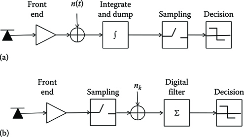
Figure 6.19 (a) Analog model of the receiver detection chain and (b) digital model of the receiver detection chain.
Naturally the field component along each of these vectors will be a complex function: the set of four real functions constituted by real and imaginary part of the field components are called field quadratures along the chosen base [19].
Setting
εk=→υk·→p+=√1−(→υk·→p−)2(6.55)
![]()
(6.55)
the four field quadratures that we will indicate as Es(t) with s = 1, 2, 3, 4 can be written as
E1(t)=N/2Σk=−N/2[√Pkcos(kΔωt+φk+Δφ){Σubukguk(t−Δτuk−uT)}εk]+n1(t)E2(t)=N/2Σk=−N/2[√Pksin(kΔωt+φk+Δφ){Σubukguk(t−Δτuk−uT)}εk]+n2(t)E3(t)=N/2Σk=−N/2[√Pkcos(kΔωt+φk){Σubukguk(t−Δτuk−uT)}√1−ε2k]+n3(t)E4(t)=N/2Σk=−N/2[√Pksin(kΔωt+φk){Σubukguk(t−Δτuk−uT)}√1−ε2k]+n4(t)(6.56)
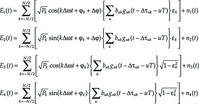
(6.56)
where the selected channel corresponds to k = 0 and nk(t) are band-limited Gaussian processes summarizing ASE accumulation and any other effect that can be described as a Gaussian noise—whose bandwidth is limited by the optical selection filter as FWM and XPM.
All the propagation effects causing signal distortion are summarized in the form of the received bit pulse gjk(t). The pulse shape depends both on the position of the pulse in the bit stream, due to the influence of the nearby bit through dispersion and similar effects introducing memory in the fiber response, and on the position of the considered channel in the WDM comb, due to the interference with nearby channels.
The photocurrent is easily evaluated on the ground of the expression of the field quadratures. After sampling, a sample of the photocurrent can be expressed as
C(th)=Rp4Σm=1E2m(th)+nr(th)(6.57)
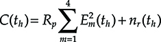
(6.57)
where nr(th) comprises all the receiver noise (i.e., thermal noise, dark current noise, and in case other noises introduced from the receiver).
The digital integrator performs the sum of a certain number of samples to produce the final value to compare with the threshold. Let us call Moe the number of samples summed up by the integrator. The integration bandwidth, that is by definition the electrical bandwidth Be, can be evaluated as the inverse of the integration time. Thus, Be = (MoeT0)−1 where T0 is the sampling rate.
Since the bandwidth of the photocurrent before electrical filtering is Bo, due to the Nyquist condition we can assume a sampling rate To = 1/B0.
It is to be noted that in real receivers, the Nyquist condition is often not fulfilled, due to the fact that it is not necessary to reproduce exactly the shape of the pulse, but it is enough to estimate the energy in the bit time.
It derives Moe = Bo/Be, where Moe represents the ratio between the unilateral optical bandwidth and the unilateral electrical bandwidth (frequently approximated with the bit rate R) and it is the same parameter we introduced to relate the optical and electrical SN ratio in Chapter 5.
Let us also remember a convention we have done in Chapter 5 and that we will use throughout the book. The noise spectral density in the optical bandwidth So is defined so that multiplied for the unilateral optical bandwidth Bo gives the noise power. Thus, in the case of a single EDFA amplifier So(ω)=ℏωcNF(G−1)![]() being NF the amplifier noise factor (this is doubled with respect to the more common definition found in literature, where the bilateral optical bandwidth is used; see Figure 5.9 at page 307).
being NF the amplifier noise factor (this is doubled with respect to the more common definition found in literature, where the bilateral optical bandwidth is used; see Figure 5.9 at page 307).
After discrete integration we have
Cw=RpMoeΣj=14Σm=1E2m(tj−wT)+nr(tj−wT)(6.58)
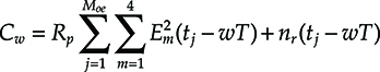
(6.58)
It is now clear that the sample in front of the threshold comparison circuit is a quadratic form of Gaussian random variable plus a Gaussian independent term.
We can assume that the Moe samples that constitute the decision variable Cw are statistically independent: this is the number of samplings at the Nyquist sampling rate of the optical signal that fit into the Nyquist sampling interval of the electrical signal (see Chapter 5). This is rigorously true if the sampling rate corresponds to the Nyquist rate and if the filters (both the optical and the electrical one) are perfect bandpass and low pass filters. Generally these conditions are only approximated by realistic systems; however, even in realistic conditions, assuming that the filters have spectral tails going to zero sufficiently fast and that the sampling is not very far from Nyquist condition, the statistical correlation among the samples can be neglected.
In this condition the characteristic function of the random variable Cw (i.e., the bilateral Laplace transform of its probability density) can be evaluated with a known method [26].
Let us individuate a set of bit patterns that allow us to manage the memory due to propagation phenomena (in general it will be a set of nine patterns of three bits as done in Section 6.1) and let us call Φj = {b}j the jth pattern. The bit that is under decision is the central bit of the pattern, that will be indicated with bcj.
The characteristic function F(s) of the decision variable conditioned to the transmission of a certain pattern has the following expression, where s = sr + isi is the Laplace variable:
Fc(s/1Φj)=exp[−(SNo(bcjMoes/(1+s))−(Q/4)s2)](1+s)2Moe(6.59)
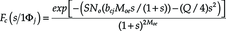
(6.59)
where
SNo is the optical SN ratio that can be written starting from Equation 6.46 as
SNo=P(bcj)SASEBo+Pnli(Φj)(6.60)

(6.60)
with the power of the optical field in the assumed hypothesis indicated with P(bcj) and the sum of the FWM power and the XPM power indicated with Pnli(Φj)
Q=σ2r/[RpSASEBo+Pnli(Φj)]
 is the ratio between the power of the receiver noise and the power of the optical noise
The BER, as in the unrepeated case, is expressed as
BER=1NpatNpatΣu=1P(ˉb−buc≠0Φu)(6.61)
(6.61)
where
ˉb![]() is the estimate of the received bit
is the estimate of the received bit
Npat = 8 is the number of patterns
In order to estimate with a suitable approximation the BER, it seems that the specific form of the decision variable can be exploited to reduce the problem to a Gaussian probability.
As a matter of fact, it seems that, after the execution of the square of the field quadratures, the term with the ASE noise squared can be neglected with respect to the beat between the ASE noise and the signal.
With this approximation the problem is effectively reduced to a Gaussian problem, but the solution is affected by an error on the order of magnitude of 3 dB: that is, in order to reach a low BER (e.g., 10−12), the needed power is estimated to be half of the correct value.
This is due to the fact that the beat term is much greater than the square noise term in average, but when an error occurs it means that the instantaneous noise power is on the order of magnitude of the signal power and in this condition it is not true that square noise is negligible. Neglecting it means more or less neglecting half the noise, when a wrong bit estimate occurs from which the magnitude of the error in the Gaussian approximation.
The terms of the sum (6.61) can be estimated correctly using the so-called saddle point approximation, obtaining a closed form expression for the error probability.
It is not within the scope of this section to demonstrate this approximation, the interested reader is encouraged to start from the bibliography regarding this point [27,28].
From an operative point of view, the saddle point approximation requires to find a real solution x0 (if it exists) of the equation
1Fc(x)∂Fc∂x+Cth−1x=0(6.62)
![]()
(6.62)
where Cth is the threshold value. If this solution is found, defining the function
Θ(x)=ln[Fc(x)]+Cthx−ln(x)(6.63)
![]()
(6.63)
the error probability is approximated as
P(ˉb=0/Φu∪buc=1)=Cth∫−∞p(c)dc≈exp[Θ(x0)]√2πΘ″(x0)(6.64)
(6.64)
and with a similar equation for (P(ˉb=1/Φu∪buc=0))![]() , where it is only necessary to change c in −c to use the approximation formula.
, where it is only necessary to change c in −c to use the approximation formula.
The saddle point approximation can be used to evaluate a very good approximation of the error probability in a very general set of cases.
It is interesting however to try to obtain a closed form approximation of the error probability at least when only the dominant ASE noise is present.
Assuming that no pattern effect is present and that thermal noise at the receiver is negligible with respect to the ASE noise, the error probability expression (6.64) relative to an intensity modulated systems with in line amplifiers simplifies as
Pe=12[Pe(0)+Pe(1)]=12e−(γSNo−2Moe)(2Moe/γSNo)2Moe+12e−SNoMoe[(X(SNo)/(1+X(SNo)))−γ(X(SNo)/Moe)][1+X(SNo)]2Moe(6.65a)
X(SNo)=−γSNo+Moe+√Moe√(γSNo+Moe)(6.65b)
![]()
where
The value of the threshold in terms of a fraction of the signal to noise ratio at the optical level is given by Cth = γSNo/Moe,
Moe is the ratio between the optical and the electrical bandwidth
Moreover, the saddle point approximation has been further simplified assuming a high SN ratio situation and SNo >> Moe (such a simplified approximation is also called Chernov bound).
This approximation is quite accurate for low values of Moe, approximately up to Moe = 5 if we look below a BER of 5 × 10⁻⁴ and up to M oe = 3 if we look to a BER below 10−12. Often in practical systems the target pre-FEC BER is on the order of 10−4 and the value of Moe is below 3; thus, this is a good approximation.
Out of these intervals, in particular for systems with a large value of Moe and a strong FEC so that the BER pre-FEC is very low, the complete saddle point approximation has to be used, that is much more accurate but produces an optimization equation whose solution has to be found numerically.
Naturally, to evaluate the BER, for each value of SNo, the decision threshold (thus γ) has to be optimized.
The BER curves obtained by Equations 6.65a and 6.65b are plotted for reference in Figure 6.20 versus SNe. If a plot versus SNo is deduced, it can be noted that increasing Moe, the BER seems to be better and better, against intuition. In reality this is not true, since it is not to forget that increasing Moe a certain value of the optical SN ratio is more and more difficult to attain due to the increase of the optical bandwidth. If this effect is evaluated it is discovered that it largely overcomes the slight decrease of the BER with Moe, so that if a plot versus the received power is done, increasing Moe the power needed to attain a given BER would increase.
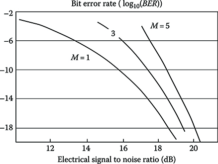
FIGURE 6.20 Ideal performance of a long-haul optical link for different values of the ratio Moe between the bilateral optical bandwidth and two times the electrical bandwidth. The equation used to plot the BER curve is the approximation reported in the text and where the approximation is not valid the curves are interrupted.
From Figure 6.20 the value of SNe when BER = 10−12 and the optical bandwidth is minimum (Moe = 1) is a bit less than 17 dB.
If a simple Gaussian model is used to evaluate the BER, but the noise variance is correctly taken into account like in [2], the required SNe to achieve a BER of 10−12 in this condition is almost exactly 17 dB. Although this assumption underestimates a bit (about 0.5 dB) the system performance, the value of 17 dB is often assumed as a design reference and we will do the same in the examples of this chapter.
Sometimes, in order to express penalties due to different transmission impairments, the so-called Q factor is used, not to be confused with the Q function.
The Q factor is defined as
Q=Q−1(BER)(6.66)
![]()
(6.66)
This definition comes from Equation 6.14 and, if the BER would be given by the relation (Equation 6.14), there would be a direct relationship between the Q factor and the SNo. In our case Equation 6.14 does not hold, and the Q factor has to be evaluated via its definition and the correct expression of the error probability.
If Equations 6.65a and 6.65b can be used, the relationship between the squared Q factor and the optical SN ratio is shown in Figure 6.21 for Moe = 2.
Up to now, we have assumed that all the amplifiers that are deployed along the line are equal, meaning that all the spans are equal.
In real system installations this is not always true. Several times, DWDM systems are installed along the route of old systems where the points of presence where amplifiers can be installed are not equally spaced.
In the presence of nonuniform spans, Equation 6.43 becomes
![]()
(6.67)
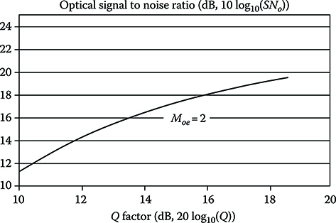
FIGURE 6.21 Relationship between optical SN ratio and Q factor for Moe = 2.
Let us assume that every in-line amplifier compensates exactly the loss of the span after it and that the booster compensates the first span while the preamplifier compensates the end terminal losses.
For the sake of simplicity, in a first approximation, let us assume that the noise factors are all equal and independent from the gain of the amplifiers. Indicating with Lv the length of the vth span, Equation 6.67 can be rewritten as
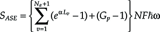
(6.68)
If the span length is variable it is a relevant problem to find the optimum span distribution, that is, the span set that minimizes the overall ASE noise.
This problem can be solved easily with the method of Lagrange multipliers, finding the minimum of (6.68) with the condition

(6.69)
L being the overall link length.
Calling γ the Lagrange multiplier the Lagrangian function is
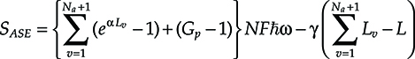
(6.70)
and the derivative, with respect to the unknown span lengths are
![]()
(6.71)
with the condition (6.69).
The only way in which all the Na relations (6.71) can be equal to zero is that all the spans have the same length. Thus, as it is intuitive, the condition of equal length spans is an extreme of the ASE function.
The fact that it is a minimum and not a maximum is readily demonstrated by applying to the equal span condition the smallest possible perturbation, that is, assuming that one span is ΔL longer than the others and, to fulfill condition (6.71), another is ΔL shorter.
Calling SASE the noise with all the span equal and S‘ASE the noise after the modification it is easily calculated
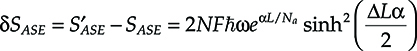
(6.72)
This quantity is always positive, demonstrating that the condition of equally long span is the optimum span distribution in the sense that it minimizes the noise power.
The situation does not change if a dependence of the noise factor on the gain is considered, as can be readily demonstrated.
It is interesting to notice that minimizing the noise is not the only meaningful way to optimize the span distribution in a DWDM long-haul system.
Due to the importance of nonlinear effects in determining the system performances, it is also meaningful to search a condition of minimal nonlinearity for a given length of the link, span number, and transmitted power.
Such a condition can be analytically expressed through the minimization of the link equivalent length that depends on the amplifier spacing.
Thus, the function to minimize is now
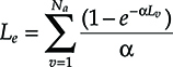
(6.73)
By repeating exactly the same procedure applied in the case of the ASE noise, it is possible to demonstrate that also in this case the minimum equivalent length is achieved when the spans have all the same length. This result is quite intuitive since if a span is longer the amplifier compensating that span has to launch more power in the fiber, causing more nonlinear effects and this is not compensated by the fact that the shorter span is less affected by nonlinearity due to the exponential growth of nonlinear efficiency with length.
From the previous discussion, it is clear that not only the situation in which all the system spans are equally long is optimum both under a noise and from a nonlinear effect point of view, but also that the performances rapidly degrade if this condition does not hold.
6.3.2 Design of Long-Haul Transmission Systems
The great part of the products offered on the market for long-haul transmission is based on DWDM and on EDFA amplifiers.
In this section, we will sketch the procedure to design from an optical point of view a system of this type. A few elements on the thermal and mechanical design will be covered at the end of this chapter.
Essentially the design of a long-haul DWDM system follows five steps:
System draft design: In the first phase the main system parameters are selected like the number of channels and their bit rate, the channel spacing, the link length, the span length, and so on. This means to position the DWDM product in a well defined category of DWDM systems.
Power budget: Starting from the first system specifications the optical power profile along the line is determined, thus selecting the components to use. At the end, the optical SN ratio is determined.
Dispersion map: Determining the dispersion map, that is, the distribution of dispersion compensating elements along the line and, in case, the presence at the transmitter and at the receiver of equalization components is a key step. It influences not only the system behavior versus chromatic dispersion, but also the impact of nonlinearities and of PMD, that in the majority of cases is equalized by electronic adaptive equalizers contemporary to chromatic dispersion.
Penalties impact: Using the penalty addition rule all the relevant penalties are added to the ideal SNo (driven only by ASE noise) to arrive to a required SNo that takes into account all the relevant phenomena. If the required SNo is smaller or equal to that estimated performing the power budget the design can go on, otherwise some elements has to be changed to match the required performance.
Simulation: The design is confirmed via simulation to understand the impact of the numerous approximations.
6.3.2.1 Erbium-Doped Optical Fiber Amplifier Amplified Systems Design
6.3.2.1.1 Power Budget
In long-haul systems, EDFA amplifiers work in deep saturation, since this allows both power stabilization along the line and minimum signal distortion.
In this condition, in-line amplifiers are characterized by an output saturation power ![]() that corresponds to an input saturation power
that corresponds to an input saturation power ![]() . This means that every in-line amplifier will inject into the line a power equal to
. This means that every in-line amplifier will inject into the line a power equal to ![]() , where αc is the coupling loss that in general is very small. At the amplifier input, the power would not be lower than
, where αc is the coupling loss that in general is very small. At the amplifier input, the power would not be lower than ![]() , due to the fact that the saturation condition has to be maintained.
, due to the fact that the saturation condition has to be maintained.
Moreover, extra losses that are located before the booster and after the preamplifier have to be accounted for. These are due essentially to the multiplexer and the demultiplexer, to connectors and patchcords connecting the different cards, and to taps used to monitor the optical signal.
Let us indicate with αM the loss of the multiplexer and the demultiplexer and αXT, αXR the extra losses at the transmitter and at the receiver respectively, with PL the optical power exiting from a transmitter after modulation and with PS PIN the input saturation power of the receiver.
Realistic values for these parameters can be found in Chapter 4 and are summarized in Table 6.2.
The power budget equations for the system are as follows:
The equation assuring that the booster amplifier is saturated so to inject into the line the correct power

(6.74)
where
nc is the number of channels
PL is the power emitted by the transmitting laser
αM is the multiplexer loss
αXT is the transmitter chain loss (containing the modulator, the passive optics, and so on)
Finally Ps,booster is the booster input saturation power.
The equation that determines the maximum span that can be covered by the in-line amplifiers (assuming that the output power of the booster is the same of that of in-line amplifiers)
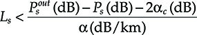
(6.75)
where
α is the fiber loss in dB/km
αc is the amplifier insertion loss
Ps and
 are the line amplifier input and output saturated power
The span length is indicated with Ls.
The equation that assures that the received power is sufficient to neglect the thermal noise of the detector but does not saturate the receiver

(6.76)
where
SRec is the receiver sensitivity
 is the saturated output power of the preamplifier
αDM is the demultiplexer loss
αRC is the whole receiving chain loss
In the case of the parameters reported in Table 6.2 Equation 6.74 is fulfilled with a channel number as high as 256 and as low as 16; thus, the transmitter power budget is almost automatically fulfilled.
Equation 6.76 is also satisfied, while the margin on the upper inequality is only 0.5 dB. This means that fluctuations in the values of the parameters risk to generate receiver saturation.
Probably, since the sensitivity is not a problem, a receiver with a higher saturation power has to be adopted, even with lower sensitivity.
Regarding the transmission line power budget, that is, Equation 6.75, spans as long as 136 km can be achieved. Increasing the span length generally the cost per Gbit/s per km of the system decreases, due to the decreasing of the number of amplifiers per unit length, but also decreases the maximum system reach. The relationship between the system length, the span length, and the amplifier number is shown in Figure 6.22.
The choice of the span length is thus a key choice to position a DWDM product on the market, being one of the main parameters governing the balance between cost per Gbit/s per km and system performances.
Figure 6.22 ASE limited system length versus the amplifier spacing. The system length is normalized to the maximum value attainable with distributed amplification. System parameters are reported in Table 6.1.
6.3.2.1.2 Erbium-Doped Optical Fiber Amplifier Amplified Systems Design: Dispersion Management
From the results shown in Section 6.2.3 it is clear that, in order to fully exploit the reach potential of DWDM amplified systems, chromatic dispersion has to be compensated.
Due to the close interaction between chromatic dispersion, SPM, XPM, and FWM, the way in which chromatic dispersion is compensated strongly influences also the way in which nonlinearity impacts transmission.
Different solutions are available to implement dispersion compensation:
Use of in-line dispersion compensators (like DCF or fiber Bragg gratings [FBG])
Pre-chirp of the transmitted pulses
Pre- and post-electronic compensation
and quite often all solutions are used together in order to find the best mix to compensate dispersion and control nonlinear effects [29,30].
In any case, in-line dispersion compensators have to be used due to the presence of nonlinearities. In a very long link, not only dispersion, but also nonlinear effects accumulate with the distance. Once a strong nonlinear distortion has been accumulated, the pulse cannot be reshaped via linear compensation and also dispersion compensation is no more possible.
Thus, dispersion has to be compensated in-line so frequently that no sensible nonlinear degradation accumulates between two nearby compensators.
In order to evaluate the effectiveness of nonlinear effect accumulation, the effective length Le is often used in unrepeated systems. The same can be done in the presence of amplifiers; since each amplifier rises the power of the optical signal, nonlinear effects could start after each amplifier so that the effective length of the amplified link is Le = na. Le0, where Le0 is the effective length of a passive fiber link and na the span number.
The only case in which in-line dispersion compensation is not needed is the case in which a new technology called electronic dynamically compensated transmission (EDCT) is used. In this section we will first analyze the approach through in-line linear compensation and after that we will describe EDCT.
In practical systems in which in-line compensation through DCF or fiber Bragg grating (FBG) is used, the amplifiers distance is sufficiently short to allow dispersion compensating modules (DCMs) to be located in the amplifiers sites, generally in between the stages of a multistage optical amplifier.
Table 6.3 Parameters of a DCF
Attenuation (dB/km) |
0.5 |
Dispersion (ps/nm/km) |
−102 |
Dispersion slope (ps/nm2/km) |
−0.2 |
Nonlinear index (m2/W) |
2.6 × 10⁻²⁰ |
Effective area (μm2) |
22 |
Three techniques can be used for in-line dispersion compensation:
Pre-compensation: The compensation module is at the beginning of the span; this means that a DCM is placed at the booster site to compensate the first span
Post-compensation: The compensation module is at the end of the span; this means that a DCM is placed at the preamplifier site to compensate the last span
Mixed pre- and post-compensation: In this case a DCM is preset both at the transmitter and at the receiver side
Several studies have been done to compare post-compensation and pre-compensation in different situations. The final result depends on the specific system setup.
In general, post-compensation performs better at the expenses of a more stringent tolerance on the compensator parameters choice. An example of this behavior is reported in Figure 6.23, where the Q factor is reported versus the compensation ratio (ratio between residual dispersion and total link dispersion) for a system transmitting a single 10 Gbit/s signal with 13 spans of 80 km of SSMF and a variable length of DCF, which is adjusted to define the compensation ratio.
The fiber parameters are given in Table 4.1, Chapter 4 for the SSMF and in Table 6.3 for the DCF. A two stage EDFA with 5 dB noise figure per stage is used in each section to regenerate losses and to host the DCF.
In Figure 6.23, experimental data reported in [31] are fitted with the performance evaluation model where the propagation of NRZ pulses through the fiber link is simulated with a program using the algorithm described in [8], that is based on the split step solution of the nonlinear propagation equation (see Section 4.39). Noise is taken into account, analytically, after the simulation of the deterministic part of the propagation.
Figure 6.23 Q factor versus the post-compensation ratio for a single 10 Gbit/s channel in a system with 13 spans of 80 km of SSMF and a variable length of DCF, which is adjusted to define the compensation ratio.
(After Peucheret, C. et al., IEEE Photon. Tech. Lett. 12(8), 992, 2000.)
Other situations exist where it is pre-compensation to be preferable, as in the examples reported in [32].
The situation changes completely if some pulse pre-distortion is implemented, either at the electrical or at the optical level.
Pre-distortion is intended to support in-line compensation in balancing the dispersion of the line. It consists in transmitting chirped pulses with a positive chirp in the case of transmission in the third window, where there is anomalous dispersion. The chirp, that can be generated by the transmitter electronics or by the optical modulator, is compensated by the first part of the fiber and provides an intrinsic robustness to dispersion.
In this case, in the great part of the systems the differences between pre- and post-dispersion compensation are much less pronounced.
Naturally, even better performances are attained when both pre- and post-compensation are used, if the overall link is suitably optimized.
As further refinement, also a combined pre- and post-compensation with individual channel compensators at the transmitter and at the receiver has been proposed [29], so attaining even better performances with respect to mixed pre- and post-compensation. The weakness of this solution is of course its cost, especially for systems with a high channel count.
From Figure 6.23, it also results that the higher value of the Q factor is realized with a certain degree of under compensation that is compensating only 98% of the line dispersion.
This result is reasonable, since a bit of residual dispersion allows SPM and XPM to be partially compensated, thus improving system performance.
Extensive study of under-compensation technique has been done [30,33,34]. The optimization technique is generally based on building a variable dispersion map, where the value of the DCF dispersion and dispersion slope are the same at each site and are the optimiza-tion parameters. Sometimes, when the requirements do not fix the amplifier sites a priori, also the span length is a third optimization parameter.
The scalar signal propagation is simulated via a numerical model and the Q factor or the SNo are evaluated using the analytical expression of the noise variance.
At this point, an algorithm is available relating the parameters to be optimized, that is, the DCF dispersion and dispersion slope and, in case, the span length, with the link quality factor.
Thus, a numerical optimization procedure is used to find the optimum parameters combination. Among traditional nonlinear optimization methods [35] the Nelder–Mead optimization procedure, also called nonlinear simplex method, seems particularly suitable for this case in which the evaluation of the objective function is quite complex [36].
Naturally, due to the fact that any optimization will require several simulation executions, a key point is to use a computationally simple simulation procedure; thus, the experience in balancing accuracy and approximations intended to simplify the computation is a key point for this optimization procedure [37, 38].
Generally, when optimizing the system, more than one local optimum exists and the choice is often guided more by the stability of the working point than by extreme optimization of the system length [31].
As a matter of fact, when implementing a design in a practical system, several considerations, besides pure performance optimization, lead the implementation choices. One of these elements is the stability of the chosen solution versus small variations of the design parameters, variations that can be caused both by tolerances of the components’ characteristics and by aging.
Another important point is the comparison between NRZ and RZ modulation. In the case of unrepeated dispersion-limited systems, RZ performs better than NRZ. This behavior is even more evident in single channel optically amplified links, due to the robustness of RZ modulation to ISI due to pulse spreading. In this case, it is even possible to improve pure RZ performances by transmitting chirped pulses to achieve more robustness to residual dispersion.
To give an example, let us consider long-haul system with length of about 4600 km and 26.2 nm optical bandwidth over SSMF. The system can support 64 channels with 50 GHz spacing.
The Q factor is plotted versus the spectral position of the selected channel in Figure 6.24.
From the plot it is clear that chirped RZ is efficient in taking under control the interplay between dispersion an XPM/SPM.
On the other hand, when DWDM is considered, the wider optical spectrum of RZ modulation impacts on channel interference. An example assuming ideal modulation and demodulation with square filters can clarify the effect. The linear sensitivity penalty for the central channel of an NRZ 10 Gbit/s comb with a spacing of 50 GHz is 1 dB, while in the case of RZ transmission with 30% duty cycle it is as high as 4 dB and to reduce the penalty to 1 dB the channels have to be separated by a gap of about 120 GHz.
In-line dispersion management can also be combined with pre- or post-electronic dispersion compensation.
Careful system design can achieve good results with time domain electronic compensators like FFE–DFE, but better results can be attained especially at high speeds using a more advanced solution. It consists in a linear EDC working on the baseband electrical pulse before modulation. It consists of three steps: FFT, multiplication for the inverse fiber frequency response, and inverse FFT [39].
This solution requires electronic processing with a very high sampling rate, arriving up to 80 Gsamples/s if applied to channels at 40 Gbit/s and it is possible only with the more recent generation of CMOS circuits.
An example of comparison between a system exploiting standard pre-compensation via DCFs and a system substituting the DCF at the transmitter with the EDC is reported in Figure 6.25 [40]. At 10 Gbit/s the performances of the traditional compensation method is superior, but at 40 Gbit/s this is no more true, due to the better accuracy with which the electronic control manages very-high-speed signals compensating the dispersion channel by channel.
A different technique based on electronic pre-compensation of nonlinear propagation distortion has demonstrated very good results allowing very long reach and stabile EDFA-based systems to be realized without using in-line compensation [40] (see Chapter 4).

Figure 6.24 Q factor versus the spectral position of the considered channel in a long-haul system 4600 km long with 64 channels and 50 GHz spacing. System parameters are reported in Table 6.1.
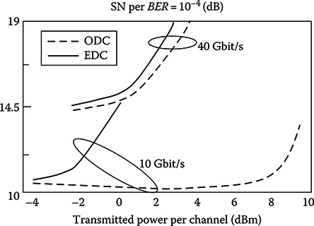
FIGURE 6.25 Comparison between standard pre-compensation via DCFs and substitution of the first DCF at the transmitter with electronic dispersion pre-compensation. System parameters are reported in Table 6.1.
(After Weber, C. et al., Optical Fiber Conference Proceedings, OFC 2009, IEEE, s.l., 2009.)
The advantages of this technique are potentially very important: adaptive electronic pre-compensation can face effectively system parameters fluctuations due to tolerances and aging; it allows much simpler EDFAs to be deployed in-line, with an evident cost advantage.
On the other hand, implementing compensation of nonlinear propagation requires complex algorithms to be implemented in a real-time signal processor with a very high sampling rate (50 GHz in the specific case).
As an example of the performance of these classes of algorithms in Figure 6.26 [18], the SNo penalty is shown versus the power launched at the transmitter into the fiber. The considered system is a single channel 1200 km long system with 15 span of 80 km each. The transmission fiber is a standard SSMF fiber with D 17 ps/nm/km, α = 0.21 dB/km, γ = (1/(W km)). No optical dispersion compensation is implemented along the line and conventional EDFAs are used. Information is coded and decoded through RZ IM-DD format without any line code and FEC.
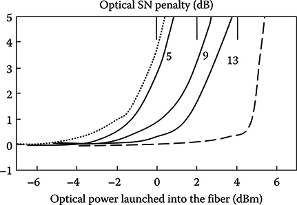
Figure 6.26 SNo penalty versus launched power in a single-channel RZ IM-DD 1200 km long system with 15 span of 80 km each using SSMF fiber with D 17 ps/nm/km, α = 0.21 dB/km, γ = (1/(W km)). Dispersion is electronically precompensated via an adaptive algorithm, no optical compensation is implemented. (After Killey, R.I. et al., IEEE Photon. Tech. Lett., 17(3), 714, 2005.)
The dotted line represents the system performances with perfect dispersion compensation and no compensation of nonlinear distortion. From this curve, it is evident that the system suffers a great performance degradation from nonlinear effects.
The solid curves represent penalty in the presence of nonlinear compensation with different orders of the look-up table addressing space (indicating the dimension of the look-up table). The performance becomes better and better with the progressive reduction of the difference between the ideal inverse propagation filter and the real processing implemented through the look-up table. The better curve is near the dashed line that represents the modulator limit.
6.3.2.1.3 Erbium-Doped Optical Fiber Amplifier Amplified Systems Design: Example of Draft Design
Here we want to apply the rules we have given in the previous sections to carry out an example of draft design of a long-haul DWDM system.
Starting from 10 Gbit/s, we state at the beginning not to use L band to avoid a too costly system.
Since L band channels are separated by C band in the fiber and require different amplifiers, the example can be easily extended to a C + L band system, only adding bands splitters when needed and all the components for L band processing.
Extended C band can allocate 90 channels at 10 Gbit/s with a spacing of 50 GHz on the ITU-T grid; thus, we will select this option as a good trade-off between cost and capacity.
We also select a span length of 70 km. With the amplifiers characteristics of Table 6.2 this is an intermediate span length (the maximum would be 136 km).
Good quality array waveguides (AWGs) are used to multiplex and demultiplex the optical channels so to arrive at a total unilateral optical bandwidth of Bo = 20 GHz (0.16 nm at 1550 nm wavelength) with Moe = 2.
The use of a FEC is almost obliged in long-haul systems and we choose the standard ITU-T FEC: the RS (255,239) that in the ideal conditions provides 6 dB of code gain.
Using Equations 6.65a and 6.65b it is easy to verify that the power budget equations for the transmitter and the receiver can be satisfied with standard DWDM quality compo-nents (see Chapter 4, the main parameters of transmitter and receiver are summarized in Table 6.1). The total ASE power is −16.4 dBm per channel, so that the ideal SNo is 24 dB and the ideal SNe = 24 dB (if Moe = 2 SNo ≈ SNe). This gives quite a margin with respect to the required 11 dB (17 from the receiver with Moe = 2 minus 6 dB of code gain) that allows the allocation of more than 8.8 dB for extra penalties due to various impairments.
The last thing to do is to select the dispersion map. We have to design quite a standard link, following literature, we will adopt a post-compensation map with a certain degree of under compensation and a per channel FFE–DFE equalization of the residual dispersion at the receiver.
Following a simple map optimization, where the only parameter to setup is the under compensation, we will under compensate for 1500 ps/nm implying a differential delay of 493 ps in the signal bandwidth and will adopt a nine taps FFE-4 tap DFE adaptive equalizer. This allows the residual dispersion to be almost completely compensated at the receiver and the SPM effect to be attenuated.
6.3.2.1.4 Erbium-Doped Optical Fiber Amplifier Amplified Systems Design: Penalties Impact
Once the DWDM system has been specified fixing its main parameters, the system power budget and dispersion map have been designed, and all the tentative specifications for the main components have been set, it is time to start to verify if the design is sufficiently robust versus all the performance impairments to meet the performance requests, that, in general, are provided in terms of a maximum attainable BER.
The draft evaluation, essentially, consists in calculating all the relevant penalties in a situation in which the considered phenomenon is the only impairment affecting the ideal system and adding the obtained penalties with the system margin to arrive at a final requirement in terms of SN ratio.
Generally, it is easier to work at the optical level, specifying the SNo, but sometimes the presence of electronic nonidealities at the receiver renders it even easier to evaluate the target SNe.
The target SN is compared, at the end, with the SN coming out from the design to verify the system is working correctly.
Naturally, it is well possible that the system does not meet the requirement in terms of SN after the first design, in this case, the main causes of distortion and noise are identified and the design is reworked again to mitigate the corresponding degradation.
We have seen in the previous sections that a long-haul system with 90 channels at 50 GHz spacing satisfies the draft requirements.
A realistic penalty allocation is reported in Table 6.4. It is to be noted that, besides impairing effects, also engineering margins are added, 3 dB of system margin that takes into account fluctuations of components specifications and imperfect design implementation and 1 dB of aging margin.
As far as the aging penalty is concerned, there are two possible approaches in considering components degradation with time. Here we have decided to perform all the calculations using end of life parameters, that have to be evaluated by components suppliers during the components qualification stage. With this choice, a further aging penalty is only a sort of second margin on a wrong evaluation of the degradation of some component.
Another approach, followed, for example, in [2], is to perform design calculations using the new components parameters. In this case, all the aging degradation has to be added at this stage. Generally, in this case, an aging penalty of 3–4 dB is considered.
The required SNo results to be 20 dB before FEC operation, smaller than the 24 dB resulting from the draft design. This gap generally exists in long-haul systems since it is used to allocate other components in the gap between the stages of in-line amplifiers, like OADMs.
Just to do an example, let us image that we have to place in four of the intermediate sites one OADM for branching that introduces a loss of 6 dB.
This loss has to be balanced by a greater gain of the EDFAs so generating more noise.
Carrying out the draft design, by introducing these new components, we see that the SNo deriving from this new analysis is equal to 21.9 dB, thus getting much nearer to the bottom line for the system working.
6.3.2.1.5 Erbium-Doped Optical Fiber Amplifier Amplified Systems Design: Simulation
The system design coming out from the considerations of Table 6.4 has been simulated using two different simulation programs.
Table 6.4 Realistic Penalty Analysis for Long-Haul 10 Gbit/s Dense Wavelength Division Multiplexing System
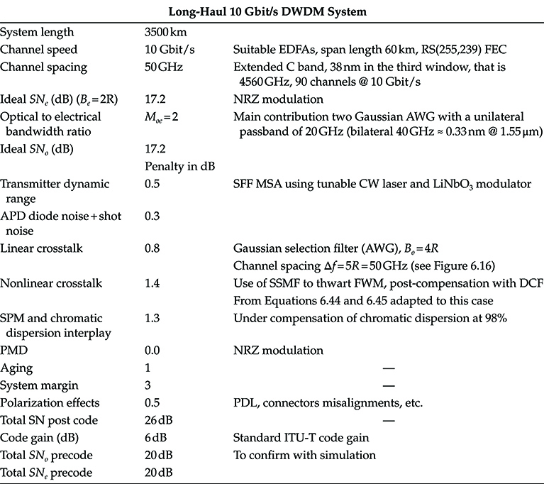
The first is a Monte Carlo simulation that is able to simulate also the noise. This is a quite accurate program, but it is computationally very complex, especially when a great number of runs have to be carried out for statistical reasons.
Running on a pc equipped with an i7 Intel processor, it is possible to arrive to an estimate of the error probability with a precision around 10% with few days of running, only if the BER is not smaller than 10−4, that means simulating the transmission of around 5 × 10⁵ pseudorandom bits.
We have also used a semianalytical program that simulates the propagation of the deterministic part of the signal and, at the end, evaluates the error probability by the saddle point approximation on the ground of the theoretical properties of the noise (naturally taking into account the real shape of the filters, and so on).
Both the programs are scalar, so that all effects related to the vector nature of the field have to be inserted at the end in a phenomenological way.
The two programs give results in a good agreement when they can be superimposed.
The simulation result in terms of BER versus the SNo are reported in Figure 6.27a for both programs, where the simulation points are interpolated with a BER function of the form (Equation 6.65) fitting the free parameters with the simulation points.
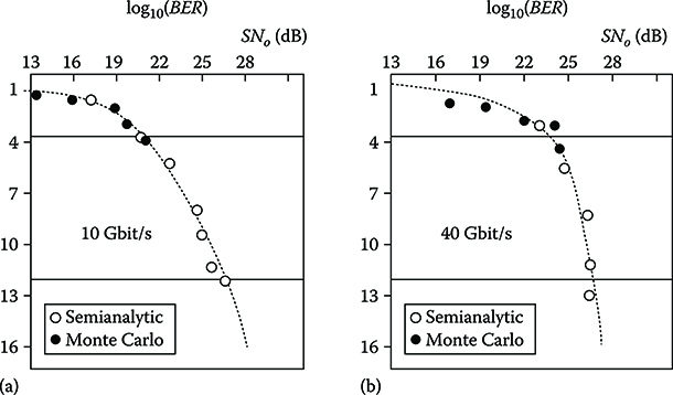
Figure 6.27 BER simulation of the system whose draft design reported in Table 6.4. Two types of simulation points are reported, Monte Carlo simulation and a semianalytic simulation where the signal propagation through the fiber and the different devices are simulated while the error probability is evaluated analytically on the ground of the theoretical noise distribution: (a) R = 10 Gbit/s and (b) R = 40 Gbit/s.
To attain the BER needed using the FEC an SNo of 15.8 dB is needed. This number of course does not take into account system margin and aging, and since the simulation is scalar, also polarization penalty is not accounted for. Thus, 5 dB have to be added a posteriori, obtaining a simulation required SN of 20.8 dB that is not far from the 20 dB obtained in the last section, taking into account all the numerous approximations.
6.3.2.2 Long-Haul Transmission at 40 Gbit/s
6.3.2.2.1 Definition and Draft Design
It is interesting to repeat the design in the case of 40 Gbit/s channels.
Choosing a channel spacing of 200 GHz the overall bandwidth of the optical link, mainly determined by the cascade of the multiplexer and the demultiplexer, can be as tight as 60 GHz, attaining Moe = 1.5 that gives a very good noise rejection.
In this case, we can allocate 22 channels at 40 GHz in the extended C band (see Table 6.5).
Reduced gain amplifiers have to be used at this speed due to the small number of channels and to the greater efficiency of nonlinear effects. The choice of the average power along the link is a strategic choice, since the right value comes out from a trade-off between the need of limiting nonlinear effects that call for a low power and the need of a high SN ratio that would bring to select a high power.
In our case, a fast look to the penalty plots relative to nonlinear effects reveals that at 40 Gbit/s a comb of 22 channels 200 GHz spaced suffers a penalty of 0.1 dB from FWM at a maximum power per channel of 0 dBm, the penalty rises at 2 dB at a maximum power per channel of 5 dBm and to 4 dB at a power per channel of 6 dBm.
Also XPM rises fast with the power per channel; it is smaller than 0.1 dB at a maximum power per channel of 5 dBm, but at 6 dBm is already slightly smaller than 2 dB.
It results that a power per channel of 5 dBm is a sort of threshold for nonlinear effects allowing to maintain the overall nonlinear crosstalk penalty at 2 dB that is a practical limit for penalty coming from a single effect for the working of our design procedure.
Table 6.5 Realistic Penalty Analysis for Long-Haul 40 Gbit/s Dense Wavelength Division Multiplexing System

Having a maximum power per channel equal to 5 dBm means to fix the output saturated power of our amplifiers at 18.5 dBm instead of 20 dBm. In practice, such a regulation can be done via software on every amplifier; thus, we can imagine using the same amplifier of Table 6.2 with a different software configuration.
We will need a high SN, since we want a total length of at least 2000 km; thus, we will chose a span length of 50 km so to reduce the ASE, as much as possible, within the constraint of a cost within market targets.
The transmitter and the receiver power budget equations are satisfied with a laser power of 13 dBm and a transmitter loss of 15 dBm, for the transmitter and a receiver loss of 10 dBm and an APD sensitivity at 40 Gbit/s of −20 dBm and an APD saturation power of −2 dBm.
The power per channel arriving on the APD is −5 dBm, sufficiently far from both sensitivity and saturation.
We can adopt at the receiver an electronic equalizer similar to that adopted in the 10 Gbit/s case.
The dispersion map, is also in this case, based on post-compensation and under compensation; the uncompensated differential group delay (DGD) is 500 ps/nm.
With the data, we derive from our draft design the ASE power in the optical bandwidth results to be −19.7 dBm, for a total SNo of 23 dB.
The ideal SNo is 20.0 dB; thus, taking into account the FEC gain, we have a great space available to accommodate all the relevant penalties.
6.3.2.2.2 Long-Haul Transmission at 40 Gbit/s: Penalty Evaluation
The next step of the system design is to evaluate all the penalties and obtain a draft estimate of the required, using the penalty addition method.
The result is summarized in Table 6.5. The required SNo results to be 22.4 dB that is smaller than the 23 dB obtained from the draft design.
In this case, only semianalytical simulation has been carried out, from which the estimate of the required SNo is essentially confirmed.
6.3.2.3 Long-Haul Transmission: Realistic Systems Characteristics
As a conclusion of this section, it is useful to review the characteristics of realistic long-haul systems as summarized in Table 6.6.
The characteristics of three different types of systems are shown, occupying different product segments in the category of long-haul DWDM systems.
The first is a system mainly designed for regional and metro–core applications, even if its characteristics allow a pure long-haul application to be feasible. It can convey a large number of different formats and data speed directly on a wavelength, and ring configurations are possible both in hub and in standard ring configuration via a flexible OADM. On the other hand, 40 Gbit/s channels are not supported.
The second system is a pure long-haul designed to be installed in the core network of a large carrier; it supports longer distances, 10 and 40 Gbit/s, and there is a possibility of supporting pure transparent branching via a fixed OADM.
Tunable OADM is also supported, in order either to drop a few channels in an intermediate site of a point-to-point link or to build optical transparent rings on long distances. Both optical channel and optical multiplex section (OMS) protections are supported.
Finally, the third system is a long-haul system also proposed for particularly high traffic regional areas.
6.3.3 Design of Ultra-Long-Haul Transmission Systems
If it is needed to design a DWDM system with a reach far greater than the number reported in Table 6.5, refining the design cannot help.
Nevertheless, the reach limitations of long-haul systems can be overcome by the combined use of EDFA and Raman amplification.
There are several possible architectures to use distributed or concentrated Raman amplification to design ultra-long-haul systems, each of which has its own design rules.
Raman amplification, can be used to provide distributed amplification as a complement to lumped EDFAs in the hybrid approach or all Raman amplification can be used, potentially both distributed and lumped.
Table 6.6 Characteristics of Realistic Long-Haul Systems Designed for Different Applications
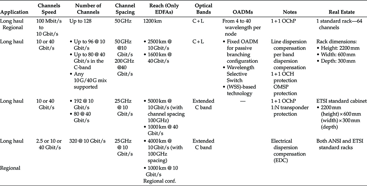
Even if hybrid approach is used, co-propagating Raman pumps, counter-propagating Raman pumps, or both can be used.
In general, the design is more complicated with respect to what is described for long-haul systems.
We will introduce the main points of the design of such systems by analyzing one of the most common architectures.
This is the architecture based on hybrid EDFA–Raman amplifiers, where the Raman pumps are located in the EDFAs locations and generate signal gain by counter-propaga-tion along the DCF.
We will assume that fiber dispersion is compensated by in-line DCF adopting under compensation to control XPM and SPM.
Due to the good Raman gain of the DCF, a single-stage EDFA is used, and the Raman pumps are propagated through the DCF to provide distributed amplification and blocked at the end of the DCF since propagating them through the SSMF used for transmission generates noise and creates limited gain due to the pumps attenuation experimented during the pass through the DCF.
The block scheme of the line site is reported in Figure 6.28.
Since the system will use extended C band, two Raman pumps are enough to achieve a flatness of the Raman gain on the order of 0.5 dB; overall gain flatness is achieved via a gain flatness filter at the output of the EDFA.
The advantages that are expected from the hybrid amplifier configuration are as follows:
Once fixed, the received power that assures the required receiver sensitivity, the Raman gain allows the optical power at the EDFA output to be reduced so decreasing nonlinear effects.
The overall optical gain is smaller and part of it is distributed; thus, less ASE is expected.
A single-stage EDFA is sufficient, also implying less ASE at the receiver.
6.3.3.1 Ultra-Long-Haul Transmission at 10 Gbit/s: Draft Design
Our scope in this section is to determine the value of the optical SN ratio before detection, given the required system length via a power budget.
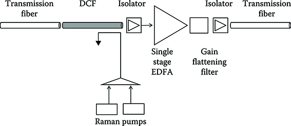
Figure 6.28 Block scheme of the line site of an ultra-long-haul system integrating a hybrid EDFA-Raman amplifier.
In this case, the system design is quite more complex, because hybrid amplifiers are to be optimized contemporary to the dispersion map, since Raman gain mainly occurs in the DCF.
We will assume that the required length of our system is around 10,000 km. In order to improve the control of dispersion and nonlinear phenomena, we will select RZ modulation with a short duty cycle: 25%. This means that the width of the transmitted Gaussian pulses at 1/e is as short as 25 ps.
Since the signal spectrum is 40 GHz large (unilateral), this choice forces to enlarge the transmission line bandwidth up to 40 GHz (unilateral, see Section 5.8.5.5) so that Moe = 4. A channel distance of 50 GHz is not feasible with this optical bandwidth; the system will support in the extended C band (38 nm) 46 channels at 100 GHz of spacing.
In order to generate such short pulses, we select a high power external cavity laser with a linewidth of 300 kHz and an emitted power of 16 dBm.
The span length is fixed to 60 km to minimize as much as possible the ASE power while remaining within a reasonable number of required intermediate sites.
In order to carry out the power budget we have to design the hybrid amplifier.
Since we are interested in a draft design that will be confirmed by simulation, the hybrid amplifier will be optimized using the Raman amplifier model reported in Chapter 4, without resorting to the much more complex model of Appendix D.
Coherently, with this design approach we will consider the penalty, due to the various noise terms, that we are neglecting in a first time as penalties in the penalty analysis.
Following the approach of Chapter 4, the gain of the Raman pumped DCF is given by
![]()
(6.77)
The parameters’ meanings are as follows (see Equation 4.86):
αD is the DCF attenuation.
LD is the DCF length.
P10 and P20 are the powers of the Raman pumps.
g1 and g2 are the corresponding normalized spectral gains.
LeD is the DCF effective length.
The optimization consists in substituting in Equation 6.77 the expressions of the Raman local gain that depends on the wavelengths and power of the pumps and on the wavelength of the signal and evaluating the average and the standard deviation of the gain over the bandwidth occupied by the DWDM comb.
In these two expressions, the power and the wavelengths of the pumps are considered variables, and the optimization is carried out by minimizing the gain standard deviation with the condition to maintain the average gain constant and equal to the value that is dictated from the system design.
This optimization can be carried out both by numerical means and by the Lagrange multipliers if an approximated analytical expression is found for the local Raman gain curve (see references in Chapter 4 for several papers on pumps optimization).
The parameters we will use for the numeric optimization and for the following system performance evaluation are reported in Table 6.7, the parameters specific of Raman amplifiers are those reported in Table 4.11.
Table 6.7 Parameters of the Hybrid Amplified 10 Gbit/s Ultra-Long-Haul System
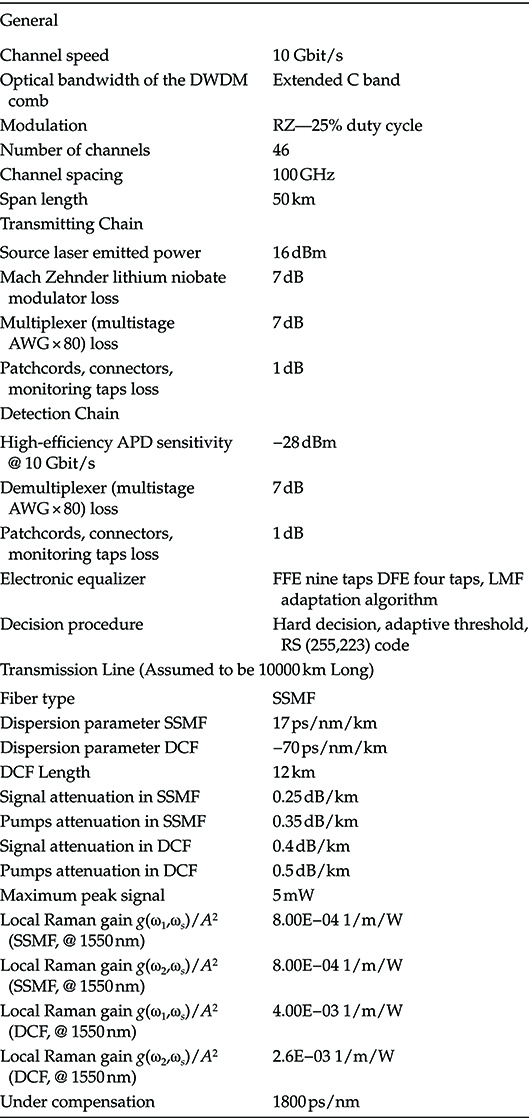
The Raman gain curve is the same DCF curve used in Chapter 4 (see Figure 4.35).
The pump wavelengths resulting from the optimization procedure are located at 1430 and at 1400 nm and the power are emitted by the pumps 330 and 290 mW.
Once the Raman distributed amplification is optimized, the design of the system can be done leveraging on two fixed numbers: the receiver sensitivity and the maximum peak power acceptable along the link to maintain nonlinear effects penalties within the limit compatible with the design.
In our case, we have assumed to have a high-efficiency APD at the receiver with a sensitivity of −28 dBm. Since we have the demux and a series of other small losses between the last EDFA and the APD, the power that has to exit from the last EDFA is equal to −20 dB (compare Table 6.7, the detection chain).
On the other hand, always assuming a link 10,000 km long, by considering under compensation for 2000 ps/nm; chirped RZ pulses with 25% duty cycle; and an electronic equalizer at the receiver composed by a nine taps FFE and a four taps DFE, the peak power along the line cannot overcome 5 mW per channel per span to maintain the SPM and the FWM related penalties within 2 dB each.
The SNo has the following expression:
(6.78)
where
Bo is the optical noise bandwidth defined mainly by the cascade of the multiplexer and the demultiplexer
Prec is the power on the receiver; this is a design parameter that has to be chosen to satisfy the receiver power budget and to optimize the system performances. In our case we select −20 dBm, against a sensitivity of −28 dBm and a saturation power of −10 dBm
arec represents the total optical loss between the output of the last EDFA amplifier and the APD, in our case the loss of the AWG and of all the monitoring taps and connectors
GB, GR, GE, Gp are respectively the gains of the EDFA booster, the Raman gain, the gain of the EDFA in-line amplifier, and the gain of the last EDFA, that is different from the others since the signal at the exit of the last span is not equal to the signal at the exit of the booster, but is equal to Prec/arec in order to minimize the ASE power
NFB, NFR, NFE, NFp are respectively the noise factors of the EDFA booster, of the Raman amplification, of the EDFA in-line amplifier and of the last EDFA
ξ is the overall gain or loss of the transmission chain, from the exit of the booster to the exit of the last EDFA and can be expressed as
![]()
(6.79)
where Ps(0) is the signal power at the output of the booster
Since, for all reasonable designs, it is the peak power of the link; it has a value PM prescribed by the nonlinear effects that in our case we have tentatively set as 5 dBm
The condition on the maximum peak power can be written as
![]()
(6.80)
where
Pl is the power emitted by the laser source
aT is the whole loss between the power source and the input of the EDFA booster; in our case, the losses of the multiplexer, the mux, the connectors, and the monitoring taps
The condition on the receiver sensitivity can be written as
![]()
(6.81)
Solving (6.80) with respect to G B and (6.81) with respect to Gp and remembering the definition of ξ, the expression of SNo becomes a function of two unknown variables: GE and GR.
Generally, since Raman distributed amplification makes less noise and operates on a signal of lower level, the optimization consists in maximizing GR, taking into account the limitations in the available power of the pumps and of the possibility of choosing different types of DCF, and then selecting consequently GE.
At this point the dimensioning of the line is ended, and all the line parameters are summarized in Table 6.8.
Table 6.8 Line Parameters after the Draft Design of the Ultra-Long-Haul 10 Gbit/s System

In order to carry out a comparison that should underline the advantages of the hybrid solution with respect to solutions based on EDFA alone, we want also design an ultra-long-haul link completely EDFA-based with the same parameters.
In this case the SNo is given by
![]()
(6.82)
where the booster amplifier is supposed to be a single-stage EDFA, post-compensation DCFs are used, as in the hybrid case, and the last EDFA is different to arrive with the correct power on the APD.
Also, in this case optimization is carried out with two constraints; the maximum power constraint is expressed by Equation 6.74, while the constrain relative to the power on the receiver is
![]()
(6.83)
After that, the design procedure is identical to the used from the design with hybrid amplifiers.
All the results of the hybrid amplification design and of the two stages EDFA design we have achieved up to now are summarized in Table 6.8.
The characteristics of the selected components and the output of the draft design allow us to evaluate the SNo at the link output that comes out 25.4 dB for the hybrid solution and 22.8 for the all EDFA solution. In both cases the FEC gain has not been accounted for, it will be considered in the penalties analysis.
A first advantage of the hybrid solution is revealed by these figures: the lower noise factor of the Raman amplifier and the automatic compensation of the DCF loss allow the ASE noise to be quite reduced.
6.3.3.2 Ultra-Long-Haul Transmission Systems: Penalties, Evaluation, and Simulation Results
Let us now define the target SNo on the ground of the various transmission impairments in both the cases we have considered.
The detail of the penalty evaluation in the two cases is reported in Table 6.9, where 21.5 dB is obtained for the hybrid solution and 23.8 dB is obtained for the EDFA solution. Thus, the 10,000 km long link can be realized with the hybrid technique (the draft design SNo was 23.5 dB) but not with a pure EDFA architecture (the design SNo was 21.5 dB). This also taking into account that a margin has to exist between the draft design SN and the requirements derived from the penalties analysis, so to accommodate the approximation uncertainty that will become clear with the simulation results.
The difference in performances is mainly in the different role of nonlinear effects, as it can be clearly deduced by the table.
In order to better appreciate the reason of this difference, the signal power behavior in a single span of the hybrid system is shown in Figure 6.29.
It is clear how the average power along the transmitted line is much lower using distributed Raman amplifiers even if the optical power entering into the EDFA at the span end (i.e., into the preamplifier in front of the receiver) is the same in both cases.
Table 6.9 Penalty Analysis of the Ultra-Long-Haul 10 Gbit/s System Realized with Two Different Architectures: Hybrid Amplification and All Erbium-Doped Optical Fiber Amplifier Amplification

This fact alleviates greatly nonlinear effects allowing a longer link to be designed.
In both cases, however, nonlinear effects determine the maximum reach in the different situations.
An interesting element to further quantify is the reach difference between the two models’ results.
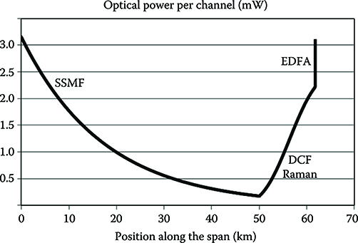
Figure 6.29 Single-channel power profile in a span of the ultra-long-haul system-based on hybrid amplification.
Doing again the dimensioning and the penalty evaluation, but maintaining the link length as a parameter, it is found that at a link length of 8000 km, the design SNo of the EDFA alone system comes out to be 23.8 dB, while the requirements coming out from the penalties evaluation is 22.0 dB. In this condition the draft design can be accepted waiting for the simulation results.
Thus, with the longer link that can be realized with the EDFA alone technique and with our design choices is on the order of 8000 km long.
Naturally, the design can be further optimized, for example, using more effective electronic compensation, introducing pre-chirp to better manage nonlinear effects, optimizing both the duty cycle and the form of the transmitted pulse, besides an optimized dispersion map and better quality amplifiers.
All these steps help to improve the system performances above what we have achieved with our simple design, but it is true for both the system architectures and the difference always remains.
Moreover, the hybrid architecture presents possibilities that are not available if all the EDFA architecture is chosen.
Raman effect can be used in a more distributed way sending the pump also in the SSMF used for transmission, both co-propagating and counter-propagating pumps can be used in the Raman amplifiers and, finally, all Raman amplification can be adopted, eliminating completely EDFA amplifiers and going much nearer to the optimum scheme of distributed amplification.
All these steps, further improve the performance of the hybrid solution so increasing the difference with the all EDFA architecture.
6.3.3.3 Ultra-Long-Haul Transmission at 40 Gbit/s
At 40 Gbit/s, all the distortions depending on the signal speed are more severe.
The draft design is carried out with the same method used in the previous section starting from a system with 18 channels at 40 Gbit/s and spaced at 250 GHz.
The large spacing is due to the fact that, to control dispersion and the other sources of ISI, RZ is very useful.
Even if the duty cycle is reduced to 33% with respect to the 25% used at 10 Gbit/s, the optical signal spectrum is 120 GHz wide so that, in order to reduce linear interference, a very large channel spacing is needed.
A very simple inspection of the FWM and XPM penalty curves in this case shows that 10,000 km are too much. For this reason we will try to design a 6500 km long system.
The draft design can be carried out with the same procedure followed in the 10 Gbit/s case and the parameters are the same, but for the transmitter loss that, due to the 40 Gbit/s modulator, is 2 dB higher and the sensitivity of the PIN photodiode that substitutes the APD used for 10 Gbit/s is −12 dBm. The PIN photodiode is used to have a higher saturation power; as a matter of fact the power per channel arriving on the PIN is −2 dBm.
The final value of the SNo derived from the draft design is 26.8 dB.
The summary of the penalty analysis for this system is reported in Table 6.10, from which a required SNo equal to 25.6 dB is obtained. The system is thus within the required performances, if the last test via simulation does not differ too much from the draft penalty analysis.
In this case, the simulation has to take into account both nonlinear propagation and the complete model of Raman amplification. In order to simplify the simulation, we have simulated all the signal distortion, by coupling the nonlinear propagation in the SSMF with the complete pumps plus signal Raman equations, eliminating the noise terms.
Naturally, pump depletion is taken into account while analyzing Raman gain.
The noise power is evaluated analytically and the saddle point approximation is used to estimate the error probability.
The results of this simulation integrated with margins and aging confirm in all the considered cases the draft design with a good.
Table 6.10 Penalty Analysis of the Ultra-Long-Haul 40 Gbit/s System

Up to now, we have underlined all the advantages of the use of hybrid amplification. However, there are also a set of issues that explain the fact that pure EDFA DWDM systems are the most diffused products on the market till today.
The first and more important point is that using Raman amplification requires high power pumps with all the induced thermal management and high operational expense related to power consumption.
It is important to remember from Chapter 2 that, in general, the main goal of carriers is to decrease the operational cost (OPEX) of the network, more than increasing the performances of the transport layer.
When deploying an ultra-long-haul system, the greater cost related to operational expenses and to the higher system cost per km and per Gbit/s have to be compared with the costs implied by realizing the link with a cheaper long-haul system, using an intermediate electronic regenerator.
Also, from the security point of view, operating systems with such powerful lasers put some problems in the procedures for units’ substitutions and maintenance in general.
6.3.3.4 Ultra-Long-Haul Systems with Electronic Pre-Compensation
The case studies we have carried out in the previous sections are intended to show the key points of long-haul and ultra-long-haul systems design.
In all the considered design variations, the compensation of the transmission line is carried out by optical means, but for the electronic compensation at the receiver.
A radically different way to solve the problem is to design a system leveraging on electronic pre-distortion via a combination of FFE–DFE and look-up table in order to deploy along the line only single-stage EDFA amplifiers to compensate losses (compare Chapter 5 for description and bibliography).
The potentialities of this strategy are all in the ability of the pre-distortion to correctly simulate and reproduce the signal propagation along the line.
From different experimental pre-distortion implementations, it results that at 10 Gbit/s the solutions based on optical compensations are quite more effective. Today, it seems that there is no viable implementation of pre-distortion circuit that at 10 Gbit/s allows about 10,000 km of SSMF to be traveled by a comb of 40 channels in extended C band.
On the other hand, the situation at 40 Gbit/s is quite different.
The reach of 40 Gbit/s systems is shorter, and nonlinear evolution is more evident.
In this situation, electronic pre-distortion is competitive from a performance point of view with optical compensation techniques [41].
Electronic pre-distortion can also be used not in alternative, but as a complement to optical compensation techniques. In this case the algorithm determining pre- distortion is a bit more complex, since all the optical compensation devices such as DCF and pre-chirping have to be simulated in back propagation, but the results can be significant.
Integrating pre-distortion with the contemporary use of look-up tables and FFE–DFE pre-compensation in the ultra-long-haul system at 10 Gbit/s analyzed in the previous section and assuming to use a nine taps FFE and a nine Taps DFE plus a 13 bit look-up table, the system can reach the impressive distance of about 13,000 km and adding also Raman co-propagating pumps in the SSMF in order to avoid excessive signal attenuation that request EDFA amplifiers, it is possible to go over 15,000 km.
However, such a complicated system, using a complex digital signal processor (DSP) per channel at the transmitter, four Raman pumps per site, and no EDFAs has quite a high CAPEX and OPEX and could be applied only in a very small number of cases, at least in terrestrial networks.
6.3.4 Single-Span Systems
In practical networks, there are a certain number of systems that have to span a few hundred kilometers, too much for unamplified systems, but a short distance for the capabilities of long-haul systems with intermediate amplifier sites.
It is to remember that increasing the number of points of presence in the network increases the operation expenses due to maintenance and other activities related to the point of presence. Moreover, in submarine networks avoiding submerged amplifiers is even more important, if possible.
Thus, it is important to understand what is the potential performance of a system having amplification only at the terminals and no intermediate site.
Since these systems have to span the maximum possible length, there are several possible architectures that seem natural: using hybrid EDFA–Raman amplification and using the DCF also for enhancing Raman efficiency, using all Raman amplification to exploit also low Raman noise factor and more distributed amplification, or using complete link pre-compensation and amplifying through single-stage EDFAs.
Moreover, the use of differential phase encoding is appealing in this kind of application due to the better receiver sensitivity.
As examples we will design three 10 Gbit/s systems: two based on all Raman amplification, one using IM, the other differential phase shift keying (DPSK), the third based on IM and complete link electronic pre-compensation with single-stage EDFA amplification.
6.3.4.1 Single-Span Systems with Intensity Modulation and All Raman Amplification
A system based on all Raman amplification tries to leverage on the specific characteristics of Raman amplifiers: low global noise factor and distributed amplification in the DCF (Table 6.11).
This last characteristic, in particular, helps to maintain a low peak power along the link contributing to take nonlinear effects under control.
Due to the fact that nonlinear effects pose at the end the final limitation to the system reach, they need a careful consideration. In all the following reasoning we will assume to have a link around 250 km long. The attenuation of 250 km of SSMF is on the order of 63 dB, a formidable amount of attenuation to be compensated.
In order to achieve a high Raman amplification efficiency, we will divide the DCF part at the transmitter and part at the receiver.
The power injected per channel into the fiber at the end of the DCF located at the transmitter determines practically the amount of nonlinear effects, since Raman amplification from pumps located at the transmitter only happens into the DCF since the pumps are extracted at the DCF end.
Being SPM and XPM critical, RZ modulation is mandatory, even if this means having a big optical bandwidth accepting more ASE noise on the detector.
To make a trade-off between robustness to ISI and ASE noise power, we will select a duty cycle of 40% that means that the Gaussian pulse at the transmitter has a full width at 1/e equal to 40 ps.
We assume also to leave a residual dispersion of about 1900 ps/nm and to pre-chirp at the modulator the pulses with the same pre-chirp used to plot Figure 6.9.
Table 6.11 Parameters Values for the All Raman Single Span Intensity Modulation and Direct Detection System
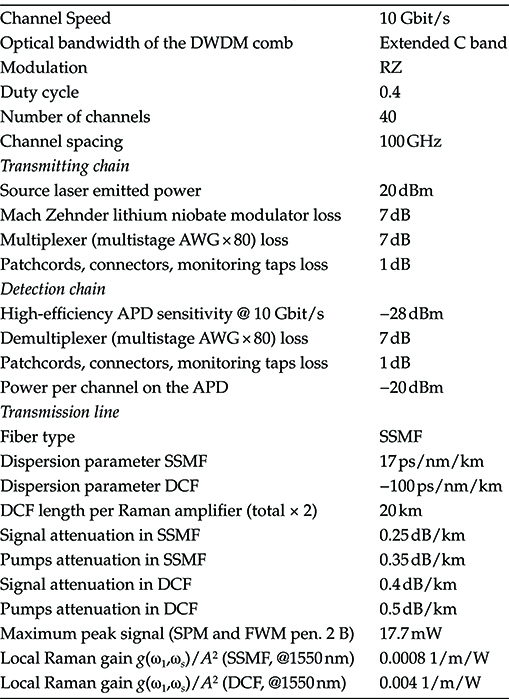
Moreover, we assume to deploy at the receiver an MLSE as those whose performances are reported in Figure 5.55, that is a very simple circuit with respect to the potential complexity of an MLSE. It is to be noticed that in our example, the MLSE is used only to estimate the channel response and to compensate it inverting the ISI.
A much more efficient use of the MLSE could be done integrating it with the FEC and the decision in a soft decision system, but for simplicity we do not consider this alternative here.
With all these elements, the maximum peak power that is allowed along the link in order to maintain the SPM/XPM penalty within 1.5 dB is 17.5 mW per channel with a total power of 700 mW considering 40 channels in the extended C band with a spacing of 100 GHz. Such a big spacing is a consequence of the RZ modulation implying a unilateral optical bandwidth Bo = 25 GHz.
As far as FWM is concerned, Equation 6.37 suitably specified to our case tells that 1 dB penalty at 100 GHz spacing on 250 km of SSMF fiber is reached at about 60 mW per channel and that at 17.5 mW we have a negligible penalty (0.2 dB).
Also the interference between channels due to Raman effect is negligible, as far as the peak power per channel along the link is limited at 17.5 mW, as it can be demonstrated by evaluating it starting from Raman gain curves.
Thus, we will deploy two sections of DCF, one at the transmitter and one at the receiver, and we will optimize their length and dispersion coefficient to have the most efficient Raman gain.
The peak power per channel on the link, that is, the power at the output of the Raman amplifier at the transmitter, is maintained at 17.5 mW per channel, regulating the power of the Raman pumps.
A scheme of the resulting link architecture is plotted in Figure 6.30.
It is to be noted that in this case the DCF has a double role. It provides dispersion compensation and enhances the Raman gain.
The two Raman amplifiers can be dealt with independently.
Solving the Raman amplifier equation (see Chapter 4) for the amplifier at the receiver we obtain the following expression of the gain:
![]()
(6.84)
where
![]()
(6.85)
and the symbols have the following meaning:
g2(ω) is the microscopic Raman gain in the DCF located at the receiver.
γs is the attenuations of the signal in the DCF.
P1 and P2 are the pumps powers injected at the DCF far end.
L2 is the length of the DCF located at the receiver.
LeD is the DCF effective length.
Analogously for the Raman amplifier at the transmitter the gain results to be with the corresponding meanings of the symbols.
![]()
(6.86)
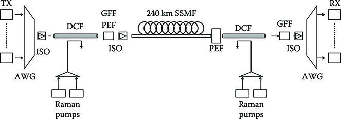
Figure 6.30 All Raman amplification single span IM-DD system architecture. TX, transmission transponders; RX, receiver transponders; ISO, isolator; DCF, dispersion compensating fiber; GFF, gain flattering filter (if needed); PEF, pump extraction filter; AWG, array waveguide; SSFM, standard single mode fiber.
The Raman gains have to be optimized both for flatness and for value.
Flatness is achieved by placing the pumps suitably as seen in Chapter 4. As far as the gain is concerned, it has to be set equal to the required value by setting the values of the pumps powers.
If the APD sensitivity is −28 dBm, it is reasonable to fix an amount of power Prec on the APD greater than the sensitivity, to be sure that the electrical noise will be negligible.
Moreover, due to the performance required to the system, we will adopt a laser with an emitted power Pl = 20 dBm; it is a DBR tunable laser with an integrated semiconductor optical amplifier (SOA) providing a gain of 8 dB that brings the power from 12 to 20 dBm.
Calling Pmax = 17.7 mW the maximum peak power per channel at the Raman amplifier at output of the transmitter, the power budget equations write
![]()
(6.87)
![]()
(6.88)
where AT, A, and Arec are the losses of the transmitting chain, the transmission fiber, and the receiving chain. In the term A, there is the link length. A fast evaluation of the parameters versus the link length suggests fixing it on the order of 300 km.
Solving these equations, the target values of the gain of the two Raman amplifiers is determined and, from the gain expression, the needed pump powers are fixed. All the results of the draft design are summarized in Table 6.12.
In determining the gain of the amplifier, the DCF length has been optimized at both sides to achieve maximum amplification.
To understand the meaning of this optimization, the behavior of the single-channel optical power is reported in Figure 6.31. Observing Figure 6.31, emerges another important feature of Raman assisted transmission that is always present, but in this case is particularly evident.
During propagation of the signal in the DCF two phenomena occur: Raman gain and attenuation due to scattering and absorption.
Table 6.12 Results of the Draft Design of the All Raman Single Span Intensity Modulation and Direct Detection System
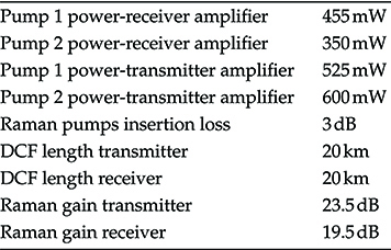
Attenuation is driven by a constant coefficient that does not depend on the pumps and on the signal, while the gain depends on the pump. This means that regulating the DCF length while the pump powers are maintained constant the Raman gain can be maximized.
This fact is also illustrated in Figure 6.32, where the Raman gain in the DCF is shown versus the DCF length.
The Raman gain is built in the first part of the DCF, up to a maximum where the pumps have produced all the possible gain, from the maximum on, the fiber attenuation overcome the gain and the gain goes down up to a final zone in which the curve is almost linear (in dBm), demonstrating that the pumps have almost completely exhausted their gain capability and the signal evolution is governed by the attenuation only.
Once determined the optimum DCF length, the dispersion parameter of the two DCF elements can be derived from the equation
![]()
(6.89)

Figure 6.31 Single-channel optical power profile in the Raman amplified single span system depicted in Figure 6.30.
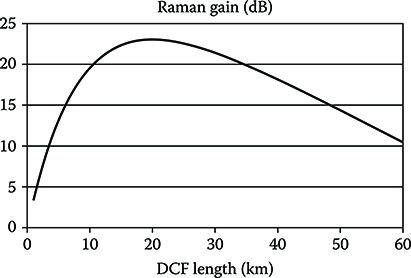
Figure 6.32 Raman gain in the DCF versus the DCF length: the pumps are maintained, fixed, and constant. The amplifier data are those relative to the system depicted in Figure 6.30.
where
D1 and D2 are the dispersion parameters of the DCF at the transmitter and at the receiver RR is the wanted residual dispersion
D is the SSMF dispersion coefficient
Since we have only one equation we can assume D1 = D2 = DD obtaining
![]()
(6.90)
The obtained DCF parameters are summarized in Table 6.12.
At this point the SNo can be evaluated by assuming a standard noise factor for the Raman amplifiers (see previous section) obtaining SNo = 18.4 dB. This figure can seem very small but it has to be taken into account that the optical bilateral bandwidth is 2Bo = 75 GHz, five times greater than the bit rate; thus, when the signal will be filtered at the bit rate with an electrical filter after detection the SNe will be larger.
After the draft design, it has to be verified by the penalties analysis.
The summary of this design phase is presented in Table 6.13. At the end, after the FEC gain, the required SNo is 18.1 dB, smaller than the design value of 18.4 dB.
A final test has to be done by simulation, whose result completely confirms the draft design.
Thus, a link 320 km long (280 km SSMF + 40 km DCF) without intermediate sites can be realized using RZ modulation and Raman amplification even if it is short of margins out of the 3 dB standard added to the penalty analysis. It is to be noted that, since pumping of the DCF is always operated from the system end, the DCF itself can be cabled and used also for transmission.
As in all the examples of this chapter, the system is not completely optimized; thus, it is to expect that better performances can be attained with a careful optimization of all the design steps.
6.3.4.2 Single-Span Systems with Differential Phase Shift Keying Transmission and Raman Amplification
In this section, we will try to improve the design we performed in the last section by changing the modulation format. Essentially, we will use differential phase modulation.
The phase of the transmitted signal is modulated using a simple phase modulator and adopting differential encoding. Let us call bj the jth transmitted bit, the signal in the jth bit interval writes
![]()
(6.91)
where ηT(t,j) is the Heaviside function that is equal to one for t ∈ (j − 1)T,jT) and zero elsewhere.
The name differential comes from the fact that the transmitted bit is encoded into the phase difference between the two consecutive symbol intervals so that θ(j) − θ(j − 1) = bjπ.
In terms of quadrature, components (6.91) writes
Table 6.13 Penalty Analysis of the All Raman Single Span Intensity Modulation and Direct Detection System

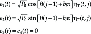
(6.92)
Differential encoding allows a very simple direct detection to be performed for DPSK signals through the receiver whose scheme is shown in Figure 6.33.
The incoming signal is split with a standard beam splitter; one of the outputs is delayed a bit time T and then the two fields are recombined with another beam splitter.
Starting from (6.91) it is easy to see that, after traveling through an amplified line, the photocurrent has the following expression:
![]()
(6.93)
where ![]() , being
, being ![]() the optical noise process, ηT(t) is the Heaviside function as defined earlier, P is the received optical power, and R the photodiode responsivity. Finally, ns(t) is the electrical and shot noise contribution.
the optical noise process, ηT(t) is the Heaviside function as defined earlier, P is the received optical power, and R the photodiode responsivity. Finally, ns(t) is the electrical and shot noise contribution.
In order to evaluate the ideal error probability it is convenient to express (6.93) via the field quadratures. Assuming as reference a polarization unit vector parallel to the instan-taneous received field polarization, the photocurrent can be written as
![]()
(6.94)
where ξ j (t) = e′j(t) + ηj t (j = 1, 2, 3, 4) are the quadratures of the received field composed by a signal contribution and an ASE contribution. The signal part of the quadrature of the field, that is, e ′j (t), is related to the transmitted quadratures via a rotation of the quadrature space induced by fiber propagation (see Chapter 4).
Since (6.94) is a quadratic form of Gaussian variables plus a Gaussian term, the method of the characteristic function can be used.

Figure 6.33 Block scheme of a DPSK receiver.
Neglecting as usual when amplifiers are used the receiver noise, the integral relating the characteristic function of the decision variable and the error probability can be solved exactly in this case providing
![]()
(6.95)
This is a very simple expression of the error probability and the required SNe for an error probability of 10−12 is 14.3 dB. This represents a gain of almost 3 dB with respect to IM, essentially, this gain is due to the fact that the average power along the line is doubled for the same peak power.
This advantage, however, is not without a price.
Not only phase modulation is affected by phase noise [8,42] that directly superimposes to the information bringing phase, but it is also more sensible to SPM, essentially for the same reason.
The draft design in case DPSK is used can be carried out with a procedure similar to that already used in the previous section.
The system parameters are reported in Table 6.14. Here it is a key to have a narrow linewidth; thus, a high emission power external cavity laser is selected as transmitter. Moreover, all the blocks constituted by splitters and delay line are supposed to be integrated into a Si–SiO2 chip so that the additional loss due to interfacing is minimum.
The parameters of the line are not reported since they are identical to the IM case.
In order to try to achieve the maximum possible distance, we also add another couple of Raman pumps into the SSMF from the receiver with the intention of limiting the signal attenuation so to decrease the global noise amount.
Since the DCF is used also for transmission of the pumps into the SSMF fiber to increase the system length, the pumps for the SSMF have to be located in the far terminal of the system and propagated up to the insertion point, that is, for 20 km, into a dedicated fiber.
Table 6.14 Parameter Values for the All Raman Single Span Differential Phase Shift Keying System
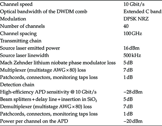
This system is called remote pumping. Since the loss of the SSMF at the pump wavelength is about 0.3 dB km; 20 km propagation is equivalent to 6 dB loss, that have to be added to the 3 dB insertion loss. Almost no loss there is at the insertion of the pump into the SSMF that transport them since we imagine that the pump lasers are sold packaged and the nominal power is the power in the fiber pigtail.
With these figures in mind, we have to add 9 dB to the remote pumps power to define the power of the pump lasers.
The scheme of the system is reported in Figure 6.34 and the single-channel power behavior in Figure 6.35. The Raman gain of this new amplifying section is again expressed by an equation like (6.92) with the parameters of the SSFM and the power budget equations becomes
![]()
(6.96)

Figure 6.34 Architecture of a single span DPSK system using all Raman amplification both in the DCF and in the transmission SSMF. TX, transmission transponders; RX, receiver transponders; ISO, isolator; DCF, dispersion compensating fiber; GFF, gain flattering filter (if needed); PEF, pump extraction filter; AWG, array waveguide; SSFM, standard single mode fiber.
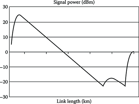
Figure 6.35 Single-channel optical power profile in the Raman amplified single span system depicted in Figure 6.34.
![]()
(6.97)
where the symbols are those of the previous section but GR3 that is the gain of the new Raman section and A′ that now refers to the passive part of the SSFM fiber, that is, L–L3 if the Raman pumps are stopped at a distance L3 from the end of the SSMF.
The gain in the SSMF is used differently from that in DCF. As a matter of fact, the pumps are stopped after a length when the power is the same it has to be at the output of the line (compare Figure 6.32 for the gain behavior with distance). The gain at that point is zero, but it is as if the length was reduced of L3 since in this part of the link the effective loss is zero.
Naturally, ASE is generated, and in order to evaluate the generated ASE this piece of fiber has to be considered as a distributed amplifier adding the noise term to the Raman equations, linearizing the equations around the noiseless solution and estimating the linearized variance of the amplified field amplitude.
This is an easy but cumbersome procedure and we do not detail it here, even because the relative noise contribution is not very important.
In the case of the DPSK the maximum power per channel changes too, due to the greater sensitivity to nonlinear phase noise becoming 15.5 mW.
The design results are summarized in Table 6.15 for 315 km of SSMF fiber so that the total system length results to be 355 km.
For this system, the draft design estimates an SNo of 17.7 dB.
The summary of the penalties analysis is reported in Table 6.16 requiring an SNo of 16.7 dB, in good agreement with the simulation estimate.
At the end, it is possible to conclude that the system is feasible and its reach is 355 km, versus the 320 km achieved with IM-DD.
Two main observations can be done comparing this example with that of the previous section: the first is that the sensitivity advantage of the DPSK is almost all counterbalanced by the bigger losses at the receiver, while the use of NRZ instead of RZ has allowed reducing significantly the noise contribution.
Table 6.15 Results of the Draft Design of the All Raman Single Span Differential Phase Shift Keying System
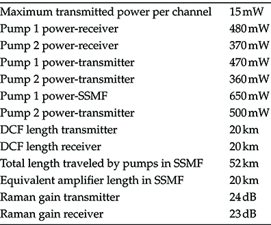
Table 6.16 Penalty Analysis of the All Raman Single Span Differential Phase Shift Keying System
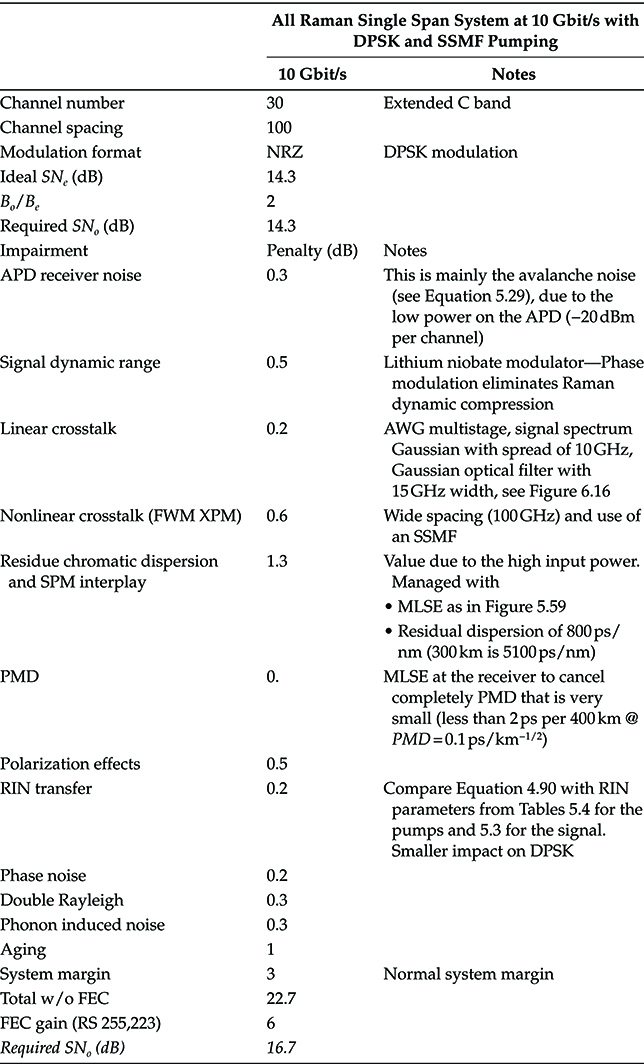
The second observation is that two additional technologies have been added in this dimensioning example: DPSK and pumping of the SSFM, both increasing the cost and the complexity of the system.
What has been gained is 35 km, which is not so much. However, in real applications, if it is very difficult or very expensive to plane in-line amplifiers (like in short submarine links) even 30 km can be the difference between realizing a project or not.
6.3.4.3 Single-Span Systems with Electronic Pre-Distortion at 10 Gbit/s
In the case in which electronic pre-distortion is used, as far as the link length is within a few hundred kilometers and no complex device is in line, it can be assumed that single-channel nonlinear effects and dispersion are completely compensated but for a fraction due to the imperfect working of the pre-distortion (finite number of bits, finite dimension of the look-up table, finite adaptation time, and so on; Table 6.17).
This uncompensated part of dispersion and nonlinear effects does not imply a penalty greater than 0.3 dB on the overall system performances at 40 Gbit/s, and an even smaller penalty at 10 Gbit/s.
Thus, the system architecture can be very simple: a single-stage EDFA booster at the transmitter and a single-stage EDFA preamplifier at the receiver, IM modulation and detection via a PIN diode due to the small loss between the preamplifier exit and the photodiode (essentially the AWG demultiplexer loss).
As usual the design starts from the power budget, considering that no dispersions have to be optically compensated.
The power budget equations are
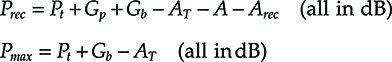
(6.98)
Table 6.17 Parameters of the Single Span Systems with Electronic Pre-Distortion at 10 Gbit/s
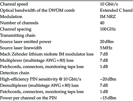
where the symbols have the usual meanings. It is to underline that, also in this case, there exists a maximum peak power per channel that can be injected into the line due to the fact that the pre-distortion device has an upper limit in its equalizing capability and if the nonlinear distortion is too pronounced or if it starts to involve nonlinear polarization rotation pre-compensation is no more possible.
The value of Pmax is much higher than in the case of previous sections and, looking at the practical implementations of electronics pre-distortion and suitably scaling the presented results [43], it can be set at 34 mW (15.4 dBm) per channel if we target a system length much longer than the effective length, that is almost always the case.
From the second power budget equation it results Gb = 16.77 dBm, the total input power being 12.77 dBm and the output power 29.54 dBm. This is not an impossible amplifier, but it is for sure not a standard booster, especially for the very high output power. It is possible that a double stage amplifier is needed, but in any case, we will assume that such an amplifier will be available.
In the second power budget equation we have two unknown parameters: the system length and the preamplifier gain.
The relation in dB between these parameters is easy: they are proportional.
A second relationship can be obtained by the SNo equation. This equation is
![]()
(6.99)
where
![]()
(6.100)
The required SNo with the adopted optical bandwidth is 17 dB, while our dimensioning gives 21 dB for 220 km transmission, allowing the accommodation of the penalties.
The penalties analysis is summarized in Table 6.18 where the required SNo is 17.8 dB, while the simulation estimates 18.2. In both cases, the value estimated in the draft design is higher, confirming the system feasibility.
Even if these results have to be considered more as an indication than as real limits, the characteristics of this category of transmission systems emerge clearly.
At 10 Gbit/s the overall performance of Raman assisted systems using mixed optical and electronic compensation performs a bit better.
However, the system based on electronic pre-distortion is much simpler, implying probably a smaller CAPEX in terms of cost per Gbit/s per km and a smaller OPEX, due to simpler maintenance, smaller cost of the spare parts warehouse, and globally better reliability.
Thus, in all the cases in which the two systems will enter in competition, the system using electronic pre-distortion is really competitive with respect to the system using Raman assisted transmission.
6.3.5 Metropolitan Optical Rings
As we have seen in Chapter 2, while in the core network the topology is generally a mesh and point-to-point transmission among complex core nodes is dominant, in the metro area ring topology is frequently used.
Table 6.18 Penalty Analysis of Single Span Systems with Electronic Pre-Distortion at 10 Gbit/s
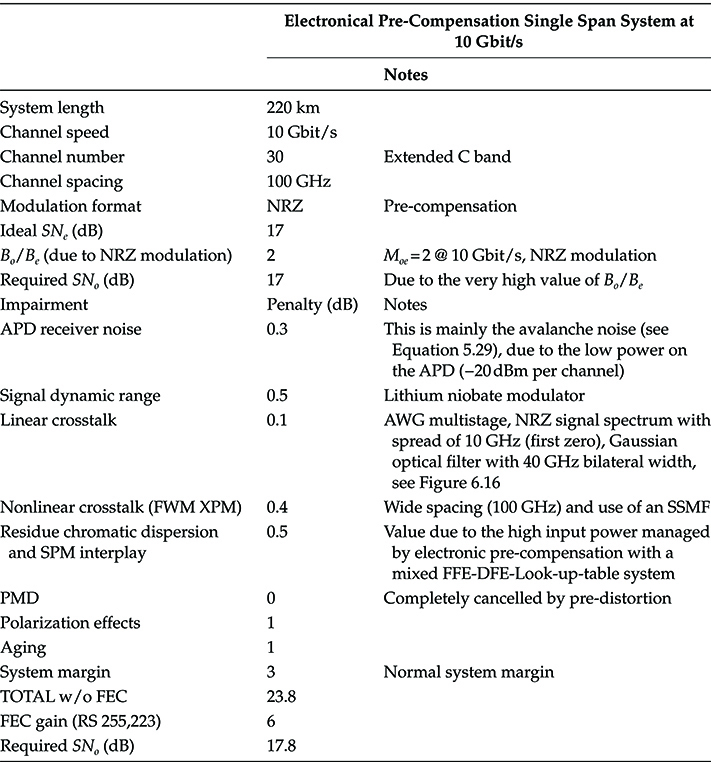
This difference reflects the different functionalities of the two networks, the first devoted to transport of signals among faraway places, the second to collect and distribute the signals generated or directed to users in the same area.
In this section, we will talk about optical rings only from a transmission point of view, while networking functionalities like wavelength routing and protection have been analyzed in Chapter 3 and the functional architecture of an OADM will be detailed in Chapter 7.
In the metro area there are two main technologies that coexist: CWDM and DWDM. As a rule of thumb, DWDM is used in the core of metro and regional network and CWDM in the metro access when single wavelength SDH/SONET systems are not sufficient to collect the traffic. However, exceptions are frequent, where, for example, CWDM is used in the core of small local networks or light DWDM systems are used to collect signals in big business centers where there is a huge amount of generated traffic.
6.3.5.1 Transmission in Dense Wavelength Division Multiplexing Metropolitan Ring
The main difference from a transmission point of view between a ring and a point-to-point link is that in a ring different optical channels, routed through the ring, generally have different sources and destinations. Moreover, the ring close topology allows spurious signal components and optical noise potentially to circulate along the ring.
The first point can represent a serious problem for amplified transmission. As a matter of fact, when designing a point-to-point system we have seen that the gain of EDFA amplifiers is flattened by the use of gain flattening filters so to exactly compensate the unbalance of the considered amplifier.
This is possible in a point-to-point system since the power of the channels traveling through a certain amplifier is fixed. The only thing that has to be managed is the progressive addition of other channels. Generally in a point-to-point system there is a rigid channel upgrade plan that prescribes the order in which the channels have to be added. In correspondence to the number of working channels, the element manager tunes the setting of the amplifiers so to maintain the required flatness.
A similar strategy is not possible in a ring network, due to the fact that the DWDM comb transiting through a generic node is formed by channels injected into the ring in different nodes and thus having very different powers. The lack of uniformity of optical power among the channels transiting in a node has an impact on the EDFAs’ gain flatness.
As a matter of fact, the gain of an amplifier depends on the signal traveling through it. To make an example, let us consider our model of Chapter 4 of the two level amplifiers and let us consider an amplifier with center wavelength at 1550 nm, microscopic saturation power of 10 mW microscopic bandwidth 155 nm and microscopic gain 5 m−1. With these parameters the linear gain is 21 dB and the macroscopic input saturation power is 0.1 mW.
This amplifier is in deep saturation if a signal of 0.5 mW power is injected at the wavelength of 1540 nm, as a matter of fact the gain of the signal is 16.7 dB.
In Figure 6.36, the gain of the signal at 1540 nm is shown versus the power of a second signal at 1460 nm, thus quite far from the first. It is evident that, increasing the second signal input power, the gain of the first signal decreases, up to compress greatly when the second is more powerful.
This behavior is due to the fact that, even if far from a spectral point of view, both the signals leverage on the same population of optically activated molecules; thus, they enter into competition inside the amplifier and the presence of the second signal de facto reduces the inverted population on which the gain of the first is built.
This phenomenon naturally also changes the spectral behavior of the macroscopic gain, depending on the power distribution of the input channels.
In Figure 6.37, the spectral gain of the amplifier is shown for different values of the two injected signals and it is clear that the percentage difference between the gain peak and the value, for example, at 1550 nm changes greatly, passing from 7.7 to 3 dB.
This behavior, even if obtained from a greatly simplified model, well represents what happens with EDFA amplifiers.
Since when a ring is deployed, it is not a priori known what will be the order in which the channels will be switched on and what will be the route of each channel; a static gain flattening cannot be used in optical rings.
Two strategies are available to face this problem: either the use of a dynamically adjustable flattening filter or a dynamic control of the channels power at the amplifier input.

Figure 6.36 Decrease of the gain of an amplifier at a certain wavelength due to the presence of a strong signal at a different wavelength.
Figure 6.37 Dependence of the gain spectrum of an ideal amplifier on the power of a strong signal transiting in the active medium.
The first solution is always possible and relies, essentially, on a set of filters, one for each spectral slice, that can be automatically adjusted by the element manager when a new channel is inserted in the ring. Naturally, these filters introduce a greater loss with respect to fixed filters.
The other solution is viable only if the channels are demultiplexed at each node, as happens when the OADM is realized with a couple of back to back AWG with optical switches in between (as shown in Figure 6.38). Here a set of variable attenuators equalize the channels before entering in the second amplification stage so to achieve a globally flat amplification.
A second issue arising in DWDM optical rings is related to the fact that, in the absence of a node where the continuity of the optical signal is interrupted, both spurious signal contributions and the ASE out of the signal bandwidth can circulate all around the ring and, if the overall ring gain is positive, could create laser action.
Figure 6.38 Block scheme of an OADM realized with AWG multiplexer/demultiplexer.
As far as ASE is considered, if no node interrupts the ring fibers continuity, it is possible to set up in one location along the ring a periodic filter that passes all the channels but stops the ASE out of the channel bandwidths.
The situation is completely different for the spurious signal components that arise from imperfect filtering of the drop OADM and continue circulation along the ring.
The situation is shown in Figure 6.39. In this figure a signal is added at node A and extracted at node C, but the extraction filter, being not ideal, allows a small part of the signal to pass through along the ring fiber until it arrives at node A again. At this point, if the suppression of the OADM is not sufficiently high, lasing action can start on the frequency λ1, ruining completely the ring working.
Naturally, here it is not possible to stop the channel bandwidth since it should be possible to have the channel wavelength available over the entire ring.
Figure 6.39 Recirculation mechanism due to imperfect optical filtering in optical transparent rings.
At this point, either a set of switches are deployed in the nodes to stop all the passing through bandwidths that are not occupied by a real channel or the ring is accurately dimensioned, taking into account aging and other potential parameter changes, to make sure that lasing condition never starts whatever is the channel load and routing.
Last but not least, in designing optical rings it has to be taken into account that potentially the signal could traverse a great number of filters, one for each traversed node.
The bandwidth of a cascade of several filters is smaller than the bandwidth of a single filter, for example, the cascade of n single pole filters has a bandwidth Bn given by ![]() , where B1 is the bandwidth of the single filter.
, where B1 is the bandwidth of the single filter.
Thus, the design of the OADM filtering characteristic has to be made carefully.
This implies also that in optical rings ASE coming from amplifiers nearer to the receiver is filtered by a larger filter with respect to the ASE coming from far amplifier, and this effect has to be taken into account when evaluating the SNo.
Just to make an example, let us imagine having a cascade of OADMs with the structure of Figure 6.38 and that the filtering characteristic of an AWG can be approximated with a Gaussian function.
Let us imagine that the signal traverses six nodes traveling from the source to the destination, that means traversing 12 AWGs, one at the source, one at the destination, and two for each intermediate node.
The overall filtering characteristic experienced by the signal is
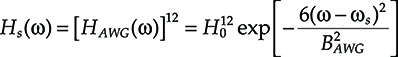
(6.101)
apart from the attenuation that is compensated by the amplifiers the overall bandwidth (in this case intended as the value at 1/e) now is ![]() so that if the design requires Bo = 4R it should be BAWG ≈ 13.85R.
so that if the design requires Bo = 4R it should be BAWG ≈ 13.85R.
However, it would be wrong to assume that Bo is also the noise bandwidth. Let us imagine, for simplicity, that the ring node is constituted by OADMs with identical amplifiers before and after (see Figure 6.39), and that the first amplifier compensates exactly the OADM loss and the second the span loss. The overall noise arriving at the receiver, if we imagine that no additional filter is present in front of the photodiode, is (see Figure 6.39 to compute how many filters the ASE generated by each amplifier traverse)
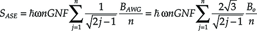
(6.102)
where j is the number of traversed spans and the spans are numbered so that the number one is the nearer to the drop node. In the aforementioned example, the optical bandwidth is 4R for the signal, but the equivalent optical bandwidth for the noise is Bn≈ 3.5Bo ≈ 14R.
This is a difference of more than 5 dB that has to be taken into account when designing the system.
Naturally, the problem can be faced by maintaining quite large the line filters and adding a noise selection filter in front of the receiver.
However, if this solution is selected, it is to take into account that in the filter bandwidth that is not occupied by the signal the ASE can circulate in the ring and the design has to carefully avoid the start of ASE lasing.
6.3.5.2 Transmission in Coarse Wavelength Division Multiplexing Metropolitan Ring
In the case of CWDM we are talking about rings without amplifiers, as a matter of fact, the CWDM occupies such a large optical bandwidth (compare Chapter 3) that it is unpractical to use amplifiers.
Moreover, in order to use uncooled sources, the channels are so spaced in frequency that there is no problem in using thin film filters to select them, avoiding any distortion due to filter cascading.
The challenge in designing CWDM systems is to satisfy the requirements in terms of power budget by maintaining the cost effectiveness that customers expect from this technology.
There exist two types of CWDM systems on the market, that are directed to different applications: pure CWDM and mixed DWDM and CWDM.
Pure CWDM systems are exclusively tailored on CWDM technology. Generally, they are simple machines whose main added value is the low cost.
These systems are generally completed with regenerators and fixed ADMs based on thin film technology and are used in the metro access area and in rural areas where the local exchanges are particularly far from the hub of the regional network.
Mixed CWDM and DWDM systems are instead capable to host on the same platform both CWDM and DWDM channels following the ITU-T standard channel allocation.
The multiplexing stage of mixed systems is generally composed by a first CWDM multiplexer, and a second DWDM multiplexer that fills with DWDM channels the CWDM passbands located in C band. This architecture is shown in Figure 6.40.
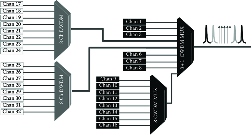
Figure 6.40 Multistage mixed CWDM/DWDM multiplexer.
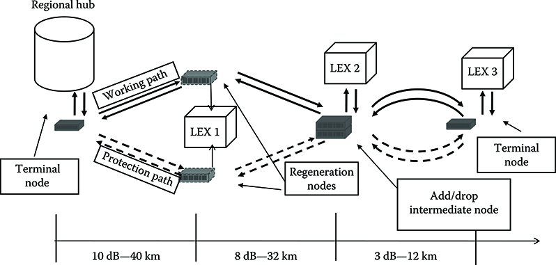
Figure 6.41 Example of CWDM system used to backhaul three small local offices to a hub.
These kinds of systems have higher cost with respect to pure CWDM, but allow slower growth after the installation using CWDM channels and faster when using DWDM configuration.
Even if CWDM interfaces at 10 Gbit/s exist and are used mainly for backhauling of remote local exchange in rural areas, more frequently CWDM wavelengths carry 2.5 Gbit/s SDH/SONET frame or directly application related formats line Fiber channel and FICON for data related applications or Gbit ethernet for small distance connections.
Typical power budgets of 2.5 Gbit/s CWDM systems are 8 dB for short-haul applications, 12 dB for long-haul, and up to 16 dB for extremely long connections.
An example of CWDM system used to backhaul three small local offices to a hub is shown in Figure 6.41. The adopted architecture is a protected bus that exploits the fibers already installed in the field. The first local exchange is reached by a complete path diversity, also using two diverse OADMs, since there were available two nearby but different sites on the ground. The second and the third local exchanges are reached with different paths but the OADM location is only one since two nearby locations were not available. In considering this architecture, it is to take into account that in rural areas, the points of presence not always are real central offices, but could also be big street cabinets where the local equipment is located.
6.4 Alternative Modulation Formats
Albeit almost all commercial equipment for optical transmission uses either NRZ or RZ modulation; a great number of other modulation formats have been devised, either to partially relieve the impact of different transmission impairments or to assure better receiver sensitivity or better wavelength selectivity.
The most promising set of different modulation formats is coupled with the use of the so-called coherent detection and is constituted by different kinds of phase modulations.
Even if in a few specific applications like single span systems, the greater sensitivity— provided by coherent detection of phase modulated signals could be useful, this kind of system never gave rise to commercial product due to their cost and to the success of IM-DD.
In facing the challenge of transmitting at 100 Gbit/s however, phase modulation and coherent detection could become a key technology and we will analyze a few applications in Chapter 9.
Among other alternative modulation formats we can remember single side band (SSB) modulation and duobinary modulation.
6.4.1 Single Side Band Modulation
The spectrum of an IM-DD signal is constituted by two sidebands and a carrier. Due to the real nature of the baseband signal, the sidebands are symmetric; thus, in line of principle, one of them is enough to reconstruct the signal at the receiver.
An SSB optical signal is generally obtained by generating a standard signal and filtering it before transmission so to eliminate one of the side bands.
An SSB optical signal ideally allows both a 3 dB SNo to be gained due to the reduced bandwidth occupation and a more dense DWDM transmission [44].
In practice, this transmission technique has not found commercial application due to the fact that at 10 Gbit/s it is not easy to control the shape of optical filters about 10 GHz wide, so to eliminate one sideband completely without affecting the carrier or the other sideband.
Moreover, it is to be noted that an SSB signal is more sensible to distortion with respect to standard IM, due to the lack of sideband redundancy that gives robustness to the standard modulation format [45].
The situation could change at 100 Gbit/s and with the evolution of electronic equalization to control signal distortions.
6.4.2 Duobinary Modulation
Duobinary modulation has been proposed for optical communications but has not experimented wide diffusion. As a matter of fact, although as any proposed method, duobinary modulation has its own advantages, it is also true that it requires more complex transmitters and the greater global cost of the system has to be compared to the economic impact of the advantages in the network design.
The duobinary modulation is a type of amplitude modulation where the bit stream is manipulated to reduce the bandwidth of the modulated signal with respect to NRZ, so reducing the impact of chromatic dispersion and PMD.
The duobinary method was first applied to electrical digital signals. It combines two successive binary pulses in the digital stream to form a multilevel electrical signal.
To easily express the duobinary encoding, let us indicate the binary bit stream with bh,k where h is the progressive number that indicates the position of the bit in the bit stream, k is zero if the bit is a zero, otherwise it is a progressive number that indicates how many ones are passed in the bit stream.
Just to give an example in the bit stream 1001101, the bits are coded in this way: b1,1 = 1, b2,0 = 0, b3,0 = 0, b4,2 = 1, b5,3 = 1, … .
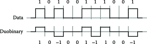
Figure 6.42 Example of duobinary coding.
Using this notation the duobinary signal dh, where h is the progressive number of the duobinary symbols, can be expressed as follows:
![]()
(6.103)
that is, if the bit is a zero, the code transmits a zero, if it is a one, the code transmits alternatively +1 and −1.
An example of duobinary coding is reported in Figure 6.42. Naturally in intensity modulation, duobinary is realized adding a bias to the modulated signal so that three different levels of power (one of them generally equal to zero) are used.
The spectrum of duobinary signal is slightly shrunk with respect to the spectrum of ordinary NRZ and much more compact than the spectrum of RZ, especially when small duty cycles are used to tolerate more pulse spreading without generating ISI.
Moreover, at the transmitter duobinary modulation can be performed by using a dual drive MZ modulator in conjunction with electrical low pass filters posed on the modulator’s driving ports and the receiver is simply a standard IM-DD receiver, with the threshold in between the zero and the first of the two levels corresponding to a one.
The advantage in terms of dispersion tolerance is not so strong, and the application of these modulations’ format is, at present, not as widespread as it was forecasted a few years ago.
6.5 Hardware Architecture of Optical Transmission Systems
In the previous section, we have analyzed a set of possible designs of optical transmission systems for application in the long-haul and metro network.
Typical quality parameters we have used to evaluate the performance have been capacity and BER.
However, it is important to recall what is derived from Chapter 2, where we arrived to the conclusion that a main target for carriers is to reduce network OPEX.
In order to reduce OPEX, it is surely important to optimize the network design using high-performing systems. As a matter of fact, decreasing the number and the complexity of central offices and points of presence is a very important task.
Once the network is optimized however, often the parameters that drive the carrier in the choice of a transmission system, among all the products that have more or less similar characteristics, are directly related to the decrease of OPEX.
Things like power consumption, real estate, easy maintenance, and safety are very often the parameters making the difference in the choice of a system among the market available products.
These considerations, strictly related to the engineering of the system, have driven strongly the evolution of DWDM systems especially after the telecom bubble end.
In this section, we will try to put the basis for a practical analysis of the engineering of an optical transmission system.
6.5.1 Mechanical Structure of a Dense Wavelength Division Multiplexing System
A typical DWDM system is mechanically hosted in one or more subracks, as shown in Figure 6.43. The same subrack is shown in Figure 6.44, without a few cards, to reveal the card positioning slides and the connectors that put the various cards in contact with the subrack backplane.
A rack supports a certain number of subracks (generally from three to five, but this is only an indication and there is a wide variety of solutions) and each subrack hosts a certain number of cards. The dimension of the rack follows detailed standards, due to the fact that they have to fit into the central office space in a better way. A diffused rack standard is the so-called 19ʹ rack, that was born in the United States, but is now diffused also in Europe and the far east [46–48].
A pictorial representation of a 19ʹ rack is presented, besides the rack standard measures, in Figure 6.45, while Figure 6.46 shows as the subracks being mounted one over the other into the rack.
Subracks on the contrary, as far as they fit into the standard rack, are largely different from system to system. Both European Standardization Institute (ETSI) in Europe and American Standardization Institute (ANSI) in the United States have defined standard subracks, but several nonstandard solutions are well accepted by the market as far as lower power and real estate sparing is demonstrated are demonstrated.
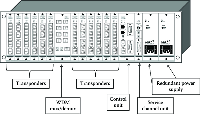
Figure 6.43 DWDM subrack: this is a metropolitan system with small cards, often long-haul and ultra-long-haul systems have higher subracks.
(Published under permission of PGT Photonics s.p.a. from Arecco. F., City8TM System Configuration Manual v 1.0. Internal PGT doc, p. 25, 2003.)
Figure 6.44 Cards allocation and backplane in a DWDM subrack.
(Published under permission of PGT Photonics s.p.a. from Arecoo. F., City8TM System Configuration Manual v 1.0. Internal PGT doc, p. 25, 2003.)
Figure 6.45 Standard measurements of the 19′ rack.
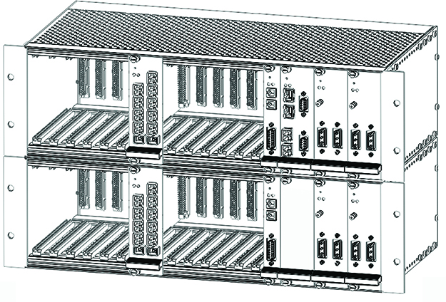
Figure 6.46 Two superimposed subracks ready to be mounted inside a 19′ rack.
(Published under permission of PGT Photonics s.p.a. from Arecoo. F., City8TM System Configuration Manual v 1.0. Internal PGT doc, p. 25, 2003.)
The cards can fit into the subrack in different ways: vertically (like in Figure 6.44) is the most frequent solution since it allows better cooling of the system, but also subrack with horizontal cards exist.
The way in which the cards fit into the sub rack is important since it is determined by the cards dimension. Larger cards, fitting horizontally into the subrack, contain a more efficient electronics design (since more components are on the same card), but make the system less flexible.
Different cards, either belonging to the same subrack or to different subracks can exchange information though the back plane.
Let us assume that no switching capability is embedded into the system (e.g., no embedded ethernet switch or no SONET/SDH ADM). In this case, the system does not need the capability to demultiplex the TDM frame of the incoming signals in order to access to the tributaries in the deterministic case or to the packets in the statistical case.
On the other hand, the incoming signal is very high capacity. A standard ultra-long-haul system can manage more than 1.2 Tbit/s capacity shared among the wavelength multiplexed 10 Gbit/s channels. In this condition, almost all the DWDM systems are designed to transfer the 10 Gbit/s channels from a card to the other using fiber patchcords on the front panel. For this reason, almost all the racks designed to accommodate DWDM and CWDM systems comprise slides and other facilities to route the external fiber patchcords in an ordered way. This can be very important to facilitate the system maintenance, due to the fact that a long-haul DWDM system can have up to 600 patchcords in a single terminal to manage its 150 wavelength channels connecting transponders to the clients and to the mux–demux.
This means also that the backplane, differently from what happens in switching equipment, does not carry the signal from one card to the other, but only the commands and other information that are passed from a generic card to the system controller.
In the architecture of a generic DWDM system we can classify the cards in three classes:
Signal cards
Control cards
Support cards
6.5.1.1 Signal Cards
Signal cards perform all the functionalities needed to manage the incoming DWDM signal in the correct way. Essentially, we have
Transponders: These are the cards where the incoming signal related to one or more channels is detected, regenerated, and retransmitted with the output power and the wavelength stability that is needed to have a correct propagation along the line. Transponders are used generally to feed the WDM system with client channels, but they can also be used (when suitable configuration is performed) to regenerate the channels in an intermediate site, when this is needed.
Even if incoming and outgoing signals have essentially the same characteristics, transponders are needed in all the high-performing systems since a DWDM system has very specific requirements in terms of power and power stability, wavelength stability, and other characteristics that the client signal generally does not have.
Naturally, open systems can exist, that is, systems that have to be used in conjunction of switching machines of the same vendor and that directly receive wellconditioned signals, since the DWDM interface is embedded in the client machine.
In this case, the transponder is substituted by a front-end card that does not perform optical-to electrical-to-optical conversion, but simply sends the received signal online after performing measurements on the signal to make sure that it is compatible with the DWDM system.
The open system solution however, up to now, does not have a great market success, especially in the incumbent carriers’ networks. As a matter of fact, this technology obliges the carrier to buy a large amount of machines performing different network functionalities from the same vendor. Even if this brings the reduction of the amount of needed hardware, it also takes away the carrier possibility of leveraging on competition to lower the prices of different machines, since at that point the process of changing either DWDM or client vendors is very difficult and expensive.
On the other hand, small competitive carriers that do not have and do not want to build a heavy company structure with test labs and research departments, frequently leave the network optimization to a specific vendor that becomes a sort of reference partner. In this case, integration of transmission and routing machines can be exploited at best. Transponders are also very important for the incumbent carriers providing high-speed transport wholesale services. As a matter of fact, in this case, the limit between the carrier network and the customer network is exactly the transponder, so that if an SLA has to be respected on both parts, the carrier needs sufficient monitoring capability to assess independently the incoming signal quality.
Multiplexers and demultiplexers: These devices are generally hosted in dedicated cards, even if their functionality is not as complex as the transponder one. The reason is that, while a transponder processes one or few channels, a multiplexer and a demultiplexer have to process all the channels that have to arrive from connectors located on the card front end. Depending on the engineering choices regarding the mechanical system design, it could be even impossible to host all the needed connectors on the front of a single card. In this case, either the card is design so to occupy more than one slot into its subrack or the mux/demux is designed as a multistage component, locating different stages in different cards.
Amplifier cards: These are the cards hosting optical amplifiers with all their structures, comprising pumps, filters, and so on. Different cards generally host different amplifiers (e.g., preamplifiers or inline amplifiers).
OADM cards: These are the cards hosting OADMs with all their structure, comprising in case, all the support needed for dynamic switching.
Protection cards: If optical protection is adopted, generally optical protection switches are hosted in specific cards.
6.5.1.2 Support Cards
Support cards perform functionalities that are needed to assure correct system working and/or monitoring, but do not involve signal processing:
The card detecting and terminating the service channel that brings control plan and central network manager information (e.g., the OMS and the ORS section headers) is a support card (see Section 3.2.7). Generally, some packet-oriented protocol is used on the management network, so that frequently this card has switching abilities that are used in the management network (e.g., it can include an ethernet switch).
The cards allowing fans installation and scaling, while the system scales in terms of channels, is another support card. As a matter of fact, only in the small systems the fans are included in the system mechanics without the possibility to scale them while the system scales.
The power supply is another support card. Depending on the system capacity, either a single power supply can be sufficient or power supply can exist in every subrack, all dependent on a central power supply. This solution, however, is adopted only when it is really needed, due to the additional real estate and complexity of the power distribution structure.
6.5.1.3 Control Cards
Control cards are essentially processors that run the network element agent and all the activities related to the control plane.
Generally, there is a single control card, having sufficient processing capability to manage all the needed software. Sometimes, due to different needs, every subrack has its own controller referring to the central controller via a local equipment network.
The central controller is also the card allowing the local craft to be connected to the system (the local craft is a light version of the element manager that is generally installed on a portable computer and allows to configure locally the network element).
Another control card is the subrack controlled. Depending on the control architecture of the system it can be a real controller or simply a switch for the equipment bus that allows different trunks of the equipment control network to be connected.
6.5.1.4 Redundancies
To reach the required network element availability, some cards are replicated twice in the system architecture and a 1 + 1 hardware protection is realized.
The network element processor is one of the cards that generally are doubled. One of the two processors works as mirror of the other, being in hot standby continuously updated so that, if the main processor fails, the second one can assure seamless network element management.
Also the power supply is generally protected by a hot standby.
6.5.2 Backplane Architecture
There are several possible solutions for the control architecture of a DWDM system, but the most common is that based on a bus communication structure. The block scheme of this architecture is shown in Figure 6.47.
The backplane is designed to create a bus for each subrack to allow all the cards that are part of the subrack to communicate each other. This bus terminates on the subrack controller.
All the subrack controllers are put in communication by the bus that connects all the subracks, that is also sustained by the backplane. In the hypothesis that more than one rack is needed, there is a bus extension that is able, from a backplane, to chain different racks.
Also in the multirack case, there is a hierarchical organization among the rack controllers so that one of them works as network element controller.
The first thing that has to be decided in designing a backplane implementing the architecture represented in Figure 6.47 is how to realize its connectivity.
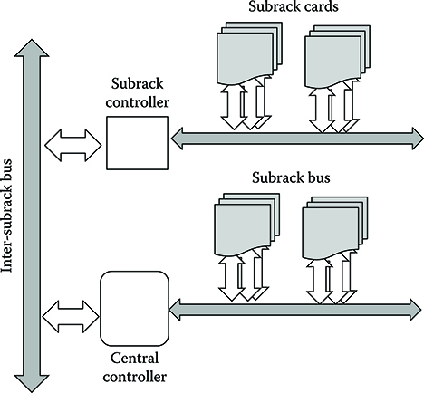
Figure 6.47 Bus-based communication architecture among the cards of a DWDM system.
Connectivity refers to how drivers and receivers are connected to the backplane and thus to the bus that allows them to communicate. In some systems it is necessary to connect multiple backplanes together. This can be done from a card to a backplane or from a card in one backplane to a card in another backplane.
After physical connection, the way in which the bus is physically implemented onto the backplane has to be defined.
In general, two types of transmission schemes are used in today’s backplanes—serial and parallel. These can be differentiated as follows:
In a parallel transmission scheme, the driver attached to the bus places bits of data in parallel signal lines onto the bus.
In serial transmission, all data is sent point-to-point in a serial stream on a single data line. In a serial backplane, to achieve the same data rates of an analogous parallel backplane, data must be sent at much higher speeds. However, differently from other network elements, like routers or switches, in DWDM systems the signal does not travel along the backplane bus; thus, the backplane speed frequently has not to be very high. Often, the backplane speed is dictated by the need of performing protection switching in the required time of a few milliseconds and to do that a speed on the order of several Mbit/s is sufficient. Serial backplanes can be implemented using special serializer and deserializer devices that convert a parallel data stream to a high-speed serial data stream and then convert it back to parallel data at the backplane output.
Each design type has the advantages and disadvantages summarized in the following. When designing a backplane, it is important to select a scheme satisfying the needs of the system where it has to be installed.
The main advantages of the parallel design can be summarized as follows:
Individual lines can be configured for control signals enabling a fast reaction time and a high degree of system and device control. This property could be very important when real-time protection switching commands have to be transmitted, especially in complex protection schemes like OChSPring.
No time delay is required for serializing and deserializing data blocks. Besides the property described in the point aforementioned, this renders the parallel design suitable for machines driven by real-time commands. Besides protection, this could be a point if a GMPLS (generalized multiprotocol label switching) control plane should take the control of all the networks (see Chapter 8).
Parallel design is common and widely used with a significant amount of industry design and implementation information available, including several standards.
While the main disadvantages of this design technique are as follows:
Significant board and system space can be required, especially with wide or high card count design that is typical of DWDM systems, where, for example, more than one hundred transponder cards can be foreseen in a fully equipped system.
Implementation costs can be high because of multiple terminations and devices, wide connectors, and high board trace counts on the backplane itself.
Line-to-line signal skew must be matched and controlled.
As far as serial design is concerned, its main advantages are as follows:
Serial data offer an adjustable approach to data rates, allowing longer cable lengths.
Fewer ground lines and signal lines are required to transmit the data from one point to another.
Serial design offers significant space savings over equivalent parallel designs. This point could be a key in highly compact DWDM designs, where real estate sparing is a system value proposition.
While the weaknesses of serial design can be summarized as follows:
A time delay is incurred, when serializing and deserializing data blocks, that has to be controlled accurately if real-time protection switching is to be performed. Moreover, if design margins are not sufficient, it could be very difficult to upgrade the system to advanced network control requiring more and more a real-time response.
Serial devices are generally more expensive than parallel backplane drivers.
Higher speeds require greater attention to signal path layout and impedance matching.
Once the bus physical wiring is defined, there are still several ways allowing multiple clients to access a shared media to transmit data among them.
Two main technologies are specifically designed to address this issue in backplanes of complex equipment. For each of these techniques, both input/output electronics chips and specific design rules are available.
Single-ended or unbalanced communication is a technique characterized by the fact that one signal from a driver is carried on one wire or on one TDM frame slot to a receiver. The receiver compares the signal to a reference level with respect to ground. If differential or balanced communication is applied, both the signal and its complement are sent from the transmitted to the receiver.
The driver sends this differential signal pair on two matched wires to a receiver, and the receiver compares the two signals with each other. This topology offers noise immunity advantages over most single-ended technologies. Because the two differential signals are compared to each other and not to a ground or logical local reference, noise or ground shifts that affect both inputs equally will be ignored by the receiver. Also, most differential technology signal swings are offset from both grounds furthering input noise immunity.
Single-ended setups are much simpler than differential ones because they use half the signal lines, but noise can be a problem. For this reason, some systems benefit from differential signaling because of its superior noise immunity.
Table 6.19 summarize the advantages and disadvantages of single-ended and differential topologies.
Last key point in backplane design is the choice of the temporization scheme among synchronous, source-synchronous, or asynchronous signal interfaces.
Table 6.19 Advantages and Disadvantages of Single-Ended and Differential Bus Topologies
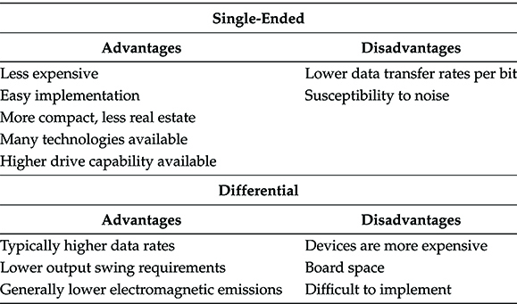
Synchronous clock is the standard architecture used in many low and medium data rate systems. The design is implemented utilizing a single clock source that provides timing for all components requiring a clock. This means that all devices throughout the system receive the clock at the same time. This implies laying out clock lines of equal length to each device. Careful layout, system timing analysis, and minimization of clock skew are critical to this design.
Source-synchronous clock architecture uses a clock generated at every driver to toggle the receiving device. This is implemented by laying out a clock line between every transceiver and driver receiver pair that passes data. To ensure correct timing, the clock lines must be the same length and have the same loading as the data lines. A system master clock is normally used to retime received data coming out of backplane boards. Since timing is now “relative” from each driver to each receiver, much of the system latency is removed as compared to a synchronous system. Data can be passed between system devices without regard to clocking times of other components in the system. The benefits of this design are a significant increase in throughput and a potential for larger backplanes, because of the elimination of latency and speed issues associated with synchronous designs. The drawback is a significant increase in clock lines—one set for each pair of data-linked devices.
Asynchronous system architecture does not use a clock. Instead of clock-synchronized data, a local “handshake” protocol between the driver and receiver is implemented. There are many different design approaches for this protocol. One example is a request signal from the driver to send data, followed by an acknowledged signal from the receiver when the data is processed. Asynchronous design can be complex and is often unique for each design implementation. However, this architecture does have some unique benefits. For example, without a clock there are no clock timing or latency issues. This lack of clocking results in a potential increase in data-transfer speeds. In an asynchronous system, only the frequency and length of the data transmission limit data-transfer speeds. Clocked systems have a constantly running clock, regardless of whether data is being transferred or processed. An asynchronous design can yield a potential reduction in power usage due to the lack of a constantly running clock. Asynchronous architecture can be complex to implement and verify, since traditional timing verification methods do not work. In addition, data streams coming from a backplane of this type still need to be retimed for system processing. Despite these potential issues, asynchronous architecture has found favor with some designs.
6.5.3 Backplane Bus Protocols
Backplane bus protocols determine—electrically and mechanically—how signals are dropped off or picked up at every device attached to the line. Protocols determine how cards pass information, the speed of data transfer, the maximum number and type of peripheral devices allowed, and the physical size and layout of the system.
In general, the choice of the correct protocol for a backplane design is a complex decision that involves many design compromises. No one solution will give the best performance in each design category.
A few systems simply adopt ethernet, allowing asynchronous transmission along the backplane to be performed with a consolidated protocol. Frequently 1 Mbit/s or 10 Mbits ethernet is enough, otherwise there is 100 Mbit/s ethernet that for sure satisfy all the communication and configuration exigencies.
At present, chips performing ethernet switching and data multiplexing and demultiplexing in the ethernet format are cheap and diffused.
The issue in using ethernet is that the protocol implements several functionalities that are not required in a backplane bus. For example, in order to use ethernet in an architecture similar to that of Figure 6.47, every subrack controller must operate versus the bus like an ethernet switch.
Moreover, in order to operate correctly, an ethernet bus needs an appropriate, although potentially quite simple, physical layer that has to be constructed via the embedded cards electronics. This is for sure a powerful solution, but sometimes too complex for the requirements.
Specific bus protocols exist for backplane applications that are able to mange backplane busses fulfilling all their requirements.
The two most diffused among these protocols are the protocols of the PCI and of the VME family. Protocols in each family come from the family generator (e.g., original PCI) via tailoring for a specific requirement, as number of managed cards.
It is out of the scope of this chapter to detail the working principles of the protocols belonging to these two families; thus, we limit our analysis to a comparison of PCI and VME pros and cons whose key results are reported in Table 6.20, and to a brief comment on the set of protocols belonging to the two families.
Table 6.20 Comparison between Two Backplane Protocols: PCI and VME
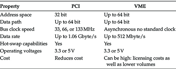
Highest number of cards on a segment: VME64. VME technology is the clear leader for the number of cards found in a segment (or continuous trace). VME is able to fit up to 21 cards on a standard 19ʹ backplane. It is important to note that, although PCI can have only four cards (eight for Compact PCI and two for PCI-X) on a segment, the technology can support up to 256 segments. However, this does have drawbacks because segments are arranged in a hierarchical tree that requires more logic bridges and longer propagation delay times, when adding additional segments to the bus.
Widest data path: VME64 (64 bit): PCI (64 bit). The width of the data path has increased to 64 bits. This size is a standard option in VME64, VME64x, VME320, PCI, Compact PCI, and PCI-X.
Fastest data rate: PCI-X (133 MHz, 64 bit, 1.06 Gbyte/s). The PCI protocol is, by far, the leader in speed. With the new PCI-X specification operating at 133 MHz and 64 bit data path, speeds of up to 1.06 Gbyte/s can be achieved. Current limitations allow only two cards on this high-speed segment and only one segment can run at 133 MHz, leaving the other segments to run at 66 MHz. The fastest competitor in the VME family is VME320, licensed by Arizona Digital, which has a bus bandwidth of over 320 Mbyte/s and a peak speed over 500 Mbyte/s.
Hot-swap capabilities: Compact PCI, PCI-X, VME64, VME64x. To hot swap means to leave the bus interface component on, or in a known state while removing or inserting a card into the system. Hot swapping or live insertion is important for customers who require systems with zero downtime. All the major protocols are adopting specifications to support hot-swap capabilities. Compact PCI and VME64 both include special mechanical configurations in the connector to make and break the ground, prebias, control, and VCC connections before the data pins touch. This allows a card to be precharged and reduces insertion transients associ-ated with noise and voltage spikes.
Low cost: PCI. Devices manufactured for the PCI specification, including Compact PCI and PCI-X, are generally less expensive than VME technology. PCI devices are an inexpensive, mass-produced bus and board standard, with literally thousands of suppliers competing at low margins. If VME is used, it will have some PCI in the final product because compatibility issues force VME system designers to include PCI in their products. With over 800 companies supporting PCI and designing cards and accessories for the PCI open specification, VME customers demand that products they buy are compatible with their current and future PCI devices.
6.5.4 System Thermal Design
As we have seen in Section 6.5.1, a typical DWDM system is constituted by one or more racks having inside subracks where the units are packed once designed on a card. In a central office racks by different systems are aligned in order to gain access to power supply and external lines.
This means that the fan tries that are designed to cool the system have to be assisted by a careful system design if they have to provide optimized performances.
The thermal design generally starts from the requirements imposed by the system mechanical design, operational environment, and heath production of the various cards. For reference, the environment requirements standardized by ETSI in Europe and by Telcordia in North America are summarized in Table 6.21.
Table 6.21 Environment Requirements for Telecommunication Equipment Standardized by ETSI in Europe and by Telcordia in North America

In particular inlets and exhaust air flows have to be carefully placed inside the system structure and correctly dimensioned.
If the rack is open, that is, no closed doors in front or in the rear, the best direction of inlets and exhaust air flows is front-bottom-in to rear-top-out, since this direction is privileged by the natural property that the air flow, hot after cooling the equipment, tends to move vertically up.
Since generally more than one subrack is stacked in a rack, the design of air flow has to take into account the cooling of each subrack.
The better solution should be independent cooling flux for each subrack.
In order to implement this kind of air flow design some space has to be foreseen between adjacent racks and this space should be organized so to render thermally independent adjacent subracks.
If a similar solution is not possible, the design can be carried out by foreseeing a single air flux traversing the whole rack, but in this case, the flux has to be sufficient to assure good cooling even taking into account the heat produced by every subrack.
This can be achieved by correctly optimizing the air flow path through the rack and the dimension and speed of each subrack fan set.
To comply with NEBS requirement the overall cooling system has to operate correctly in three situations:
Worst case environment conditions (taking into account to calculate temperature and humidity, the height on the see) with fans at full speed and a single dirty filter in all installation conditions.
One fan failure with the other fans at full speed and the environment at 40°C.
Standard conditions (environment at 40°C) with fans at minimum speed, assuring on all the components a temperature compliant with their foreseen live.
Thus, the thermal design has to be carried out taking into account effective compliance tests.
The approach to the analysis of the cooling capacity of a given air flux is in principle, easy starting from classical fluid motion theory and thermodynamic equations.
In particular, assuming laminar motion and calling z the vertical direction, we can write the following equations for the air flow motion and the heath exchange with the surrounding system:
(6.104)
where
![]() is the so-called Lagrangian derivative and represents the fact that the equations of motions are all written in the moving fluid particle reference frame
is the so-called Lagrangian derivative and represents the fact that the equations of motions are all written in the moving fluid particle reference frame
![]() is the fluid particle velocity in the absolute reference frame (as defined in the Navier– Stokes approach)
is the fluid particle velocity in the absolute reference frame (as defined in the Navier– Stokes approach)
p is the pressure in the direction of the fluid motion (assumed laminar)
ρ is the fluid density
g is the gravity constant on the earth surface
Q is the heath density
T is the local temperature
cp is the air specific heath at constant pressure
It is apparent that, even if the nature of the air motion in a well-designed cooling system allows several simplifications in the motion equations, solving the aforementioned equations system with suitable boarder conditions is a formidable mathematical problem.
The system designer has two possible options at his disposal.
The first consists in using a trial and error design procedure supported by a specific software tool that allows, once the air flow is designed and the power dissipation of each part of the system is fixed, to solve the aforementioned equations, numerically so deriving the regime temperature of all the system parts.
Commercial tools exist to do that and the probability of finding a suitable technical solution in a short time is completely dependent on the experience and physical insight of the designer that is able to start from a tentative solution sufficiently near to the optimum.
On the other hand, if some support in the first design is to be devised before analyzing the proposed structure with a software tool, either Equation 6.104 have to be drastically simplified or some heuristic rule has to be used.
A heuristic model that is largely used is that of concentrated constant heat circuit, that in electronic engineers groups is easily adopted due to its similarity with concentrated electronic circuit analysis.
In this model, every point in which a heath exchange is performed is modeled as a concentrated constant heat circuit, so talking in general of heat impedance and, in particular, of heat resistance, for example.
In this simple model, each part of the system that can be considered uniform from a thermal point of view (e.g., an interface card could be considered uniform in a first approximation, taking as a reference the worst card position, where the heat is generated by the transmitter) and that is in contact with a heat sink is characterized by a thermal resistance θT, so that the relationship between the temperature difference T between the card and a static heat sink and the power Pd the card can dissipate can be written as
![]()
(6.105)
Naturally, the thermal resistance depends not only on the system element, but also on the way it is connected to the heat sink. In our case, where there is a forced air flow that works as heat sink, there are technical graphics that, starting from measurements and analytical evaluations, give the thermal resistance existing between a subsystem and the air flow in the hypothesis of a complete immersion of the subsystem in the air flow, so that the air is in contact with every part of the subsystem. One of these graphics is reported in Figure 6.48.
At this point the procedure for the design is the following:
Construct the thermal equivalent circuit remembering to insert all the heat resistances (also that related to a simple flow of the air along a space in the rack, since heat is exchanged with the metallic rack walls; Figure 6.49).
For each subsystem evaluate the desired working temperature and the dissipated power.
Construct the heat circuit model of the system also considering the incoming and outgoing air temperatures that are determined by the environmental conditions; the heat transfer model coming out are similar to the scheme of Figure 6.49, where a subrack with a few mounted cards is represented with a heat circuit.
For each subsystem evaluate starting from Equation 6.90 and the heat circuit model the heat resistance that allows the power dissipation at the required temperature.
Figure 6.48 Example of plot providing the thermal resistance versus the air flow speed in conditions of laminar flow.

Figure 6.49 Example of simplified thermal equivalent circuit for a DWDM rack.
From each heat resistance determine the corresponding, needed air flow from graphs similar to Figure 6.48 or from specific software.
Design the air ducts, so to assure in every point of the system, at least the required flow, often the higher value of the air flow is the only considered and a worst case design is carried out trying to assure the same flow to all the system parts.
At the end of the design, the cooling system should be always analyzed with software solving numerically the fluid thermodynamic equations to verify with a less approximated model the expected performance.
REFERENCES
1.. Agrawal, G.P., Fiber Optic Communication Systems, Wiley, New York, s.l., 2002, ISBN-13: 978-0471215714.
2.. Ramaswami, R., Sivarajan, K.N., Sasaki, G.H., Optical Networks: A Practical Perspective, 3rd edn., Morgan Kaufmann, San Francisco, CA, s.l., 2010, ISBN: 9780123740922.
3.. Senior, J., Optical Fiber Communications: Principles and Practice, 3rd edn., Prentice Hall, Essex, U.K., s.l., 2008, ISBN-13: 978-0130326812.
4.. Smith, D.R., Digital Transmission Systems, Kluwer Academic Publishers, Norwell, MA, s.l., 2004, ISBN: 1402075851.
5.. Recommendations, ITU-T. M.21xx Series.
6.. Recommendations, ITU-T. G.821, G.826, G.828, G.829.
7.. Cotter, D., Observation of stimulated Brillouin scattering in low loss silica fiber at 1.3 μm, Electronics Letters, 18, 495–496 (1982).
8.. Iannone, E., Matera, F., Mecozzi, A., Settembre M., Nonlinear Optical Communication Networks, Wiley, New York, s.l., 1998, ISBN-13: 978-0471152705.
9.. Boyd, R.W., Nonlinear Optics, Academic Press, San Diego, CA, 2008, ISBN-13: 978-0123694706.
10.. Chaplyvy, A.R., Limitations on lightwave communications imposed by optical fiber nonlinearities, Journal of Lightwave Technology, 8, 1548–1557 (1990).
11.. Loudon, R., The Quantum Theory of Light, 3rd edn., Oxford Science Publications, Oxford, s.l., 2000, ISBN: 0198501765.
12.. Bulow, H., System outage probability due to first- and second-order PMD, IEEE Photonics Technology Letters, 10(5), 696–698 (1998).
13.. Winzer, P.J., Kogelnik, H., Ramanan, K., Precise outage specifications for first-order PMD, IEEE Photonics Technology Letters, 16(2), 449–451 (2004).
14.. Watkins, L.R., Zhou, Y.R., Dispersion compensation for long-haul, high capacity NRZ systems by pre-chirping and optimum receiver signal processing. In IEE Colloquium on High Capacity Optical Communications, May 16, London, U.K., s.n., 1994.
15. Ito, T., Yano, Y., Ono, T., Emura, K., Pre-chirp assisted normal dispersion region transmission for highly marginal dense WDM transoceanic system. In Proceedings of the Optical Fiber Conference, February 22, 1998, San Jose, CA, s.n., 1998.
16.. Nakazawa, M., Yamamoto, T., Tamura, K.R., 1.28Tbit/s-70 km OTDM transmission using third-and fourth-order simultaneous dispersion compensation with a phase modulator, Electronics Letters, 36(24), 2027–2029 (2000).
17.. Xia, C., Rosenkranz, W., Electrical mitigation of penalties caused by group delay ripples for different modulation formats, IEEE Photonics Technology Letters, 19(13), 1041–1135 (2007).
18.. Killey, R.I., Watts, P.M., Mikhailov, V., Glick, M., Bayvel, P., Electronic dispersion compensation by signal predistortion using digital processing and a dual-drive Mach–Zehnder modulator, IEEE Photonics Technology Letters, 17(3), 714–716 (2005).
19.. Betti, S., De Marchis, G., Iannone, E., Coherent Optical Communications Systems, Wiley Interscience, New York, s.l., 1995, ISBN: 0471575127.
20.. Tkach, R.W., Chraplyvy, A.R., Forghieri, F., Gnauck, A.H., Derosier, R.M., Four-photon mixing and high speed WDM systems, IEEE Journal of Lightwave Technology, 13, 841–849 (1995).
21.. Harboe, P.B., da Silva, E., Souza, J.R., Analysis of FWM penalties in DWDM systems based on G.652, G.653, and G.655 optical fibers, World Academy of Science, Engineering and Technology, 48, 77–83 (2008).
22.. Xu, B., Brandt-Pearce, M., Comparison of FWM- and XPM-induced crosstalk using the Volterra series transfer function method, IEEE Journal of Lightwave Technology, 21(1), 40–53 (2003).
23.. Bellotti, G. et al., XPM-induced intensity noise in WDM compensated transmission systems. In European Conference on Optical Communications, Madrid, Spain, Vol. 1, pp. 425–426, 1998.
24.. Salehi, J.G., Proakis, M., Digital Communications, 6th edn., McGraw Hill, New York, s.l., 2008, ISBN-13: 978-0071263788.
25.. Trischitta, P.R., Varma, E.L., Jitter in Digital Transmission Systems, Artech House, Norword, MA, s.l., 1989, ISBN: 089006248X.
26.. Morse, P.M., Feshbach, H., Methods of Theoretical Physics—Part 1, McGraw Hill, New York, 1935.
27.. Mazo, J.E., Satz, J., Probability of errors for quadratic detectors, Bell Systems Technical Journal, 44(11), 2165–2187 (1965).
28.. Helstrom, C.W., Performance analysis of optical receivers by saddle point approximation, Transactions on Communications, 27(1), 186–191 (1989).
29.. Najto, T., Terahama, T., Shimojoh, M., Yorita, T., Chikama, T., Suyama, M., Pre- and postdispersion compensation in long haul WDM transmission systems, IEICE Transactions on Communications, E83-b(7), 1409–1416 (2000).
30.. Costa, N.M.S., Cartaxo, A.V.T., Influence of dispersion compensation granularity on the XPM-induced degradation in NRZ-IM-DD WDM links at 10 Gbit/s per channel with 50 GHz of channel spacing. In Ninth International Conference on Transparent Optical Networks, ICTON ‘07, IEEE, Roma, Italy, 2007.
31.. Peucheret, C., Hanik, N., Freund, R., Molle, L., Jeppesen, P., Optimization of pre- and post-dispersion compensation schemes for 10-Gbits/s NRZ links using standard and dispersion compensating fibers, IEEE Photonics Technology Letters, 12(8), 992–994 (2000).
32.. Frignac, Y., Antona, J.-C., Bigo, S., Hamaide, J.-P., Numerical optimization of pre- and in-line dispersion compensation in dispersion-managed systems at 40 Gbit/s, Optical Fiber Communication Conference and Exhibit, OFC 2002, IEEE, s.l., pp. 612–613, 2002.
33.. Killey, R., Thiele, H.J., Mikhailov, V., Bayvel, P., Optimisation of the dispersion map of compensated standard-fibre WDM systems to minimise distortion due to fibre nonlinearity, In I.P. Kaminow and T. Li (Eds.) Optical Fiber Telecommunications IV, Academic Press, San Diego, CA, Invited Chapter, 2001.
34.. Hayee, M.I., Willner, A.E., Pre- and post-compensation of dispersion and nonlinearities in 10-Gbps WDM systems, IEEE Photonics Technology Letters, 9(9), 1271–1273 (1997).
35.. Sun, W., Optimization Theory and Methods: Nonlinear Programming, Springer, New York, s.l., 2009, ISBN-13: 978-1441937650.
36.. Avriel, M., Nonlinear Programming: Analysis and Methods, Dover Publishing, Mincola, NY, s.l., 2003, ISBN: 0486432270.
37.. Sinkin, O.V. et al., Optimization of the split-step Fourier method in modeling optical-fiber communications systems, IEEE Journal of Lightwave Technology, 21(1), 61–68 (2003).
38.. Pachnicke, S., Chachaj, A., Helf, M., Krummrich, P.M., Fast parallel simulation of fiber optical communication systems accelerated by a graphics processing unit. In International Conference on Transparent Optical Networks, ICTON 2010, Munich, Germany, Paper Th.B1.5, IEEE, s.l., 2010.
39.. Weber, C., Bunge, C.A., Winter, M., Fibre nonlinearities in 10 and 40 Gb/s electronically dispersion precompensated WDM transmission. In Optical Fiber Conference OFC/NFOEC 2009, San Diego, CA, IEEE, s.l., 2009.
40.. Yamazaki, E., Inuzuka, F., Yonenaga, K., Takada, A., Koga, M., Compensation of interchannel crosstalk induced by optical fiber nonlinearity in carrier phase-locked WDM system, IEEE Photonics Technology Letters, 19(1), 9–11 (2007).
41.. Weber, C., Bunge, C.-A., Petermann, K., Fiber nonlinearities in systems using electronic predistortion of dispersion at 10 and 40 Gbit/s, Journal of Lightwave Technology, 27(16), 3654–3661 (2009).
42.. Huang, J.-A. et al., Impact of nonlinear phase noise to DPSK signals: Experimental verification of a simplified theoretical model, IEEE Photonics Technology Letters, 17(10), 2236–2238 (2005).
43.. Killey, R.I., Watts, P.M., Glick, M., Bayvel, P., Electronic dispersion compensation by signal pre-distortion. In Proceedings of the Optical Fiber Communications Conference OFC 2006, Paper OWB3, IEEE/OSA, s.l., 2006.
44.. Laurencio, P., Medeiros, M.C.R., Analysis of optical single side band systems employing optical amplifiers. In The International Conference on “Computer as a Tool”, EUROCON, 2007, IEEE, s.l., pp. 1017–1022, 2007.
45.. Takano, K., Sakamoto, N., Nakagawa, K., SPM effect on carrier-suppressed optical SSB transmission with NRZ and RZ formats, Electronics Letters, 40(18), 1150–1151 (2004).
46.. International Electrotechnical Commission (IEC), Basic dimensions of front panels, subracks, chassis, racks and cabinets, IEC 60297-3-101, 1st edn., 2004–2008.
47. International Electrotechnical Commission (IEC), Subracks and associated plug-in units, IEC 60297-3-101, 1st edn., 2004–2008.
48.. International Electrotechnical Commission (IEC), Injector/extractor handle, Keying and alignment pin, Connector dependent interface dimensions of subracks and plug-in units, Dimensions and design aspects for 1 U chassis, IEC 60297-3-101, 1st edn., 2004–2008.