4
Verilog Vision Simulator
In designing a vision chip, testing is more than simply checking for the correct relationship between the actual output and the desired output, given the test vectors, as in the case of ordinary digital circuit design. The vision chip must deal with very large amounts of data and high data rates such as video frames, as well as various image formats such as bitmap, jpg, and tiff. The data rate in a stereo vision chip is expected to be two to three times higher than it is in an ordinary single video system. Moreover, the vision chip might be part of a large vision system that consists of various types of software and hardware. To build such a vision system, we have to interconnect two heterogeneous systems: vision software and a vision chip. Therefore, we have to move away from the conventional test bench concept to the more specialized concept of the vision simulator. This vision system will function as an interface to the chip and vision programs, in a similar fashion to open source computer vision (OpenCV). Generally, the simulator will perform a long sequence of operations: provide images to the chip, perform preprocessing, supply the intermediate preprocessed data to the chip, retrieve the result from the chip, perform post-processing, and provide the final output. In addition to simulation, the simulator by itself can be used as a research tool to develop vision algorithms. Thus, with a simulator, we can build a complete vision system comprising vision software and hardware.
In developing a vision simulator, we may choose one of two approaches. One approach is to use the Verilog system functions and tasks, provided in Verilog 2005 (IEEE 2005). As we learned in the previous chapter, the system tasks and functions are similar to those in C. We can use these functions to read images from files, apply preprocessing, feed the processed image to the chip, collect the results from the chip, and write the results to another file. Another approach is to use the Verilog Procedural Interface (VPI), in which Verilog code invokes C code, which then invokes the Verilog system tasks and functions, for image input and output, preprocessing, and post-processing. This method requires that packages be built both in Verilog and C, using libraries defined in VPI. Unfortunately, this approach is very challenging and appears impractical, compared to the tremendous investment required. Instead, it is more efficient to use the first approach, aided by the vision package, OpenCV (OpenCV 2013).
In this context, this chapter introduces two simulators: a Vision Simulator (VSIM) that is based on scan lines and another that is based on video frames. Both systems are fundamentally based on Verilog system tasks and functions and OpenCV. The processing element in VSIM is generally designed so that more detailed algorithms can be implemented on it. Among VSIMs, line-based VSIM (LVSIM) is designed for algorithms that process images line by line, as in DP. Frame-based VSIM (FVSIM) is more general; it allows neighborhood and iterative computations, as needed in relaxation and BP algorithms.
4.1 Vision Simulator
In general, the simulator must contain the following three components: a main program in C/C++, a Verilog HDL simulator, and a processing element (Figure 4.1). The main program is a general image processing software written in a high-level language, the processing element is the target design for synthesis, and the Verilog HDL simulator is the interface between the main program and the processing element.
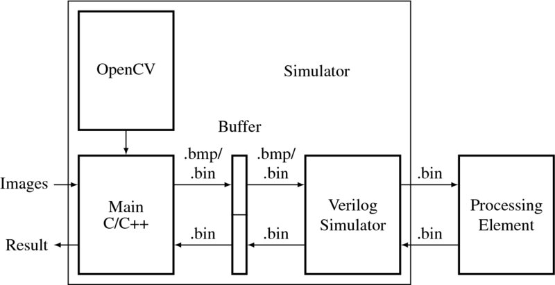
Figure 4.1 The structure of a vision simulator
The main program is the front-end of the system, and as such receives a set of images, executes some vision algorithms, including preprocessing, and writes the intermediate result to a file, so that the Verilog simulator can access the intermediate result, process it, and store the result of processing in another part of the file. The main program then reads this result from the file, processes it further using vision algorithms, conducts post-processing, and outputs the final result. During the processing, the main program may use other vision packages, such as OpenCV. The OpenCV package represents an image by an object, Mat, and thereby manipulates it, using various vision processing operations. In its location between the main program and the processing element, the Verilog simulator reads information from the buffer file and supplies it to the processing element. At the end of processing, it reads the result from the processor and writes it back to the file. The processing element receives the raw image data from the Verilog simulator, processes it, and returns the result to the Verilog simulator. In this manner, the three components form a loop, consisting of forward and backward paths from the outside into the chip.
It is obvious that the programming paradigms of the three components are different: the main program is written in C/C++, the Verilog simulator is written in Verilog System tasks/functions, which may not be synthesized, and the processing element is written in Verilog HDL, which must be synthesized. To make components exchange data flawlessly without concern for their internal implementation, we must make the data format between any two interfacing systems the same. The input to the main program is a set of images, taken from still cameras or video cameras, which are encoded in various formats (Wikipedia 2013b). The format of the output from the main program is even more varied: data, feature maps, disparity maps, optical flow maps, other map types, and images. Between the main program and the Verilog simulator, the image must be coded in a common format, such as bitmap (i.e. a file with the .bmp extension) or raw image (i.e. a file with the .bin extension, signifying binary data). Between the Verilog simulator and the processing element, the data format must be raw (i.e. it should have a .bin extension).
In simple cases, the main program can be disregarded and the Verilog simulator alone used to manage the bitmap or raw image stored in the file. If image formats are a problem, OpenCV may not be necessary, because they can be converted to bitmap or raw image by dedicated image converters. In a sophisticated system, the main program can be used to connect the Verilog simulator and OpenCV, and transfer data between them, without relying on files. This scheme can be accomplished using the VPI in Verilog-2005 (also DPI in SystemVerilog), which links the high-level programming and Verilog (also SystemVerilog). A C program can be compiled with VPI constructs using vpi_user.h and called from the Verilog simulator as user defined procedures (UDPs). However, the programming complexity involved in building the complicated interface needed is not worth the time investment required. A more practical approach is to use a simple buffer (i.e. a file) between the main program and the Verilog simulator, as described above. The systems are loosely coupled but are very versatile in dealing with general cases. Under these assumptions, we develop the main program and the Verilog simulators, as well as a general form of processing element in the ensuing sections.
4.2 Image Format Conversion
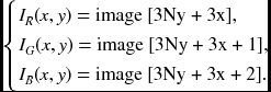
Because several different programming environments must be linked, a common file format for exchanging the data in files is necessary. Two basic forms are used: raw format and bitmap format. (Let us use the file extension .bin for raw image files, and .bmp for bitmaps, as per convention.) The raw format is a 1D array of pixels in Verilog data format, obtained by rearranging the 2D image (Figure 4.2). In mathematical terms, an image is represented by an array, I = {I(x, y)|x ∈ [0, N − 1], y ∈ [0, M − 1]} where each pixel is in the RGB color model, I = {(R, G, B)}, and in Verilog is represented by an array, ‘reg [7:0] image [0:3*`N * `M-1];’, where `M and `N are parameters representing row and column, respectively. For a pixel, the corresponding Verilog array is
If the image is stored in a 2D Verilog array, `reg [7:0] image [0:2][0:`N-1][0:`M-1];', the mapping would be more natural. However, we prefer to use the 1D array representation because the coordinate transformation for this type of array is not very difficult. Furthermore, frequent image transfers between modules is involved, which necessitates a simple counter over more complicated counters.
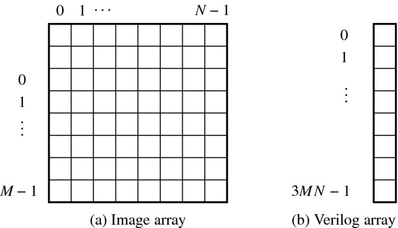
Figure 4.2 Raw file format
Image processing also needs neighborhood computation. Between the image and the Verilog array, the relationship is
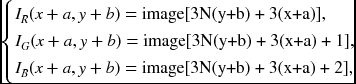
where (a, b) is the offset of the neighbor from the pixel (x, y). For a set of images, I = {I1, I2, …, IT}, the raw map is a stack of the images ‘reg [7:0] image [0: 3*`N*`M *`T-1].’
For a pixel, image[i], within an image, the neighborhoods are (i + 3, i − 3, i + 3N, i − 3N) (i.e. east, west, south, north) for a four-neighborhood system and (i + 3, i + 3N + 3, i + 3N, i + 3N − 3, i − 3, i − 3N − 3, i − 3N, i − 3N + 3) (i.e. east, southeast, south, southwest, west, northwest, north, northeast) for an eight-neighborhood system. In stereo matching or motion estimation, two or more images must be compared. For the neighborhoods (i + 3, i − 3, i + 3N, i − 3N) in the first image, the corresponding pixels in the second image are (3MN + i + 3, 3MN + i − 3, 3MN + i + 3N, 3MN + i − 3N) for a four-neighborhood system. For an eight-neighborhood system, the pixels, (i + 3, i + 3N + 3, i + 3N, i + 3N − 3, i − 3, i − 3N − 3, i − 3N, i − 3N + 3), in the first image, correspond to the pixels, (3MN + i + 3, 3MN + i + 3N + 3, 3MN + i + 3N, 3MN + i + 3N − 3, 3MN + i − 3, 3MN + i − 3N − 3, 3MN + i − 3N, 3MN + i − 3N + 3), in the second image. This relationship can be expanded to other neighborhood systems.
In addition to the raw format, we use the bitmap file format to facilitate the exchange of data between modules in the simulator. The bitmap image file format (Wikipedia 2013a) (a.k.a. BMP and DIB) is a raster graphics image file format used to store bitmap digital images, independently of the display device. The bitmap file format is capable of storing 2D digital images of arbitrary width, height, and resolution, both monochrome and color, in various color depths, and optionally with data compression, alpha channels, and color profiles. The values are stored in little-endian format. The general structure comprises fixed-size parts (headers) and variable-size parts appearing in a predetermined order (Table 4.1).
Table 4.1 Major components in the Bitmap format
| Parameter | Value |
| File size | {image[5],image[4],image[3],image[2]} |
| Offset | {image[13],image[12],image[11],image[10]} |
| Width (pixels, no padding) | {image[21],image[20],image[19],image[18]} |
| Height (pixels, no padding) | {image[25],image[24],image[23],image[22]} |
| Bits per pixel | {image[31],image[30],image[29],image[28]} |
| Raw data size (padding) | {image[37],image[36],image[35],image[34]} |
cf. Numbers in decimal. The notation, {A,B} means the concatenation, AB.
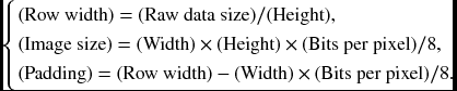
Although the format contains many parts describing every detail of the image, only the parts necessary for our needs are listed in the table. The offset is the address where the pixel array begins. Ordinarily, the RGB format is ‘8.8.8.0.0,’ which means that the pixel array is a 24-bit RGB block, with each color represented by one byte. The order of the colors is B, R, G, from lowest to highest addresses. Normally the pixel order is upside-down with respect to the normal raster scan order, starting in the lower left corner, going from left to right, and then row by row from the bottom to the top of the image.
In calculating the variables, padding bytes (from zero to three), which are appended to the end of the rows in order to increase the length of the rows to a multiple of four bytes, must be considered. Therefore, when the pixel array is loaded into memory, each row begins at a memory address that is a multiple of four. From the header information, we have to derive the parameters: row width, excluding padded bits, image size, and the number of padded bits, which sometimes may not be available in the header. The parameters can be derived using the following equations:
The bitmap file is more useful than a file that is in the raw format because it can be viewed on a monitor. On the other hand, the raw format is required internally by modules that manipulate the raw array in image processing. Therefore, there has to be an interface for converting the bitmap to raw format and then reconstructing the raw image to bitmap file format. The former processing is required when the image processing is going to be applied, whereas the latter is required when the result is going to be observed. The header and the derived parameters are needed for such image conversions. In the vision simulator, the two conversions are major operations, which simulate the camera output and monitor display.
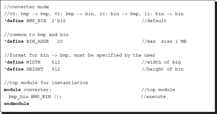
Let us build a module that converts file formats between BMP and BIN (binary). Although, there are many image converters and binary editors, the Verilog-based converter is especially necessary because it is the part of the vision simulator into which images are fed and which displays the resulting image format. Incidentally, through this design, we can understand both image formatting and Verilog coding. The internal function of the converter is illustrated in Figure 4.3. The input to the converter may be either of the two formats, bitmap or binary. Likewise, the output may be either of the two formats. If a bitmap file is converted to binary, the file must be stripped into header and binary, where only the binary part is output. If a binary file is converted to bitmap, the file must be transposed and an appropriate header synthesized, using the data in the Verilog header, and added. The key operation is the header extraction and synthesis, extraction of the binary, and pixel order inversion.
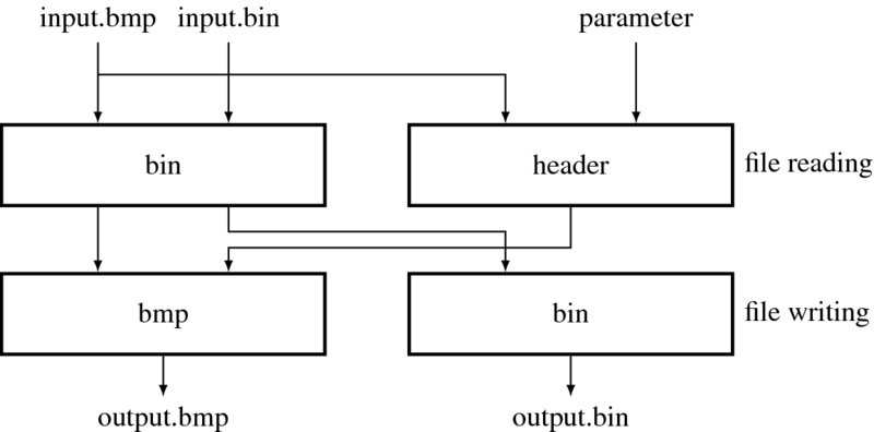
Figure 4.3 An image converter in Verilog
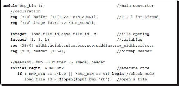
We divide the design into three parts: header, file reading, and file writing parts. The header specifies three pieces of information: The first piece of information is the conversion mode: bmp to bmp, bmp to bin, bin to bmp, and bin to bin, which is specified by the parameter BMP_BIN. The second piece of information defines the maximum size of the files. The third piece of information is the size of the bin file, which carries only the image intensities. This information is essential when the bin format is to be converted to bmp and bin formats.
Listing 4.1 Converter: header and top module (1/3)
The first part (header) also contains an instantiation of the main module, bmp_bin. No signal, such as clock or reset, is necessary as this design is executed by the Verilog simulator, unencumbered by synthesis constraints.
The second part (file reading) is for reading bmp and bin files. This file reading part must provide two pieces of information: header and binary data. For the bmp file, the header and binary parts are all in a single file and thus must be extracted and stored. The header contains all the information about the image, such as width, height, and bits per pixel, as mentioned previously. The padding bits may or may not be provided in the header and must thus be computed and stored. The bitmap header is used when the converter converts the internally stored binary file into a bitmap file.
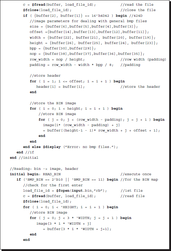
Listing 4.2 Converter: reading file (2/3)
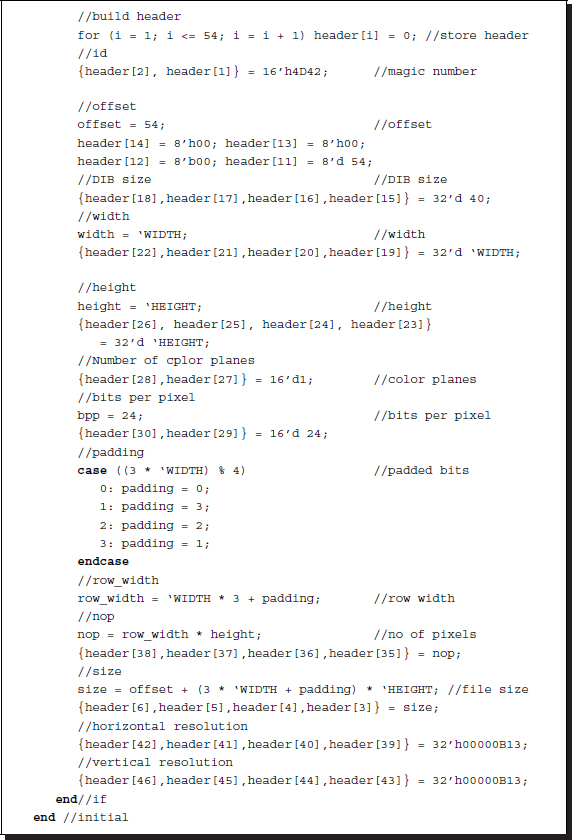
The bin file has no image information and so this must be provided by the Verilog header file. In the reverse processing of the bitmap file, the header is composed from the various bitmap fields. The bitmap header is used when the converter converts the internally stored binary file into an external bitmap file. This processing is particularly needed in order to observe the output of the vision simulator, such as maps, disparity maps, and optical flow maps, as we shall see.
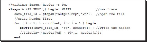
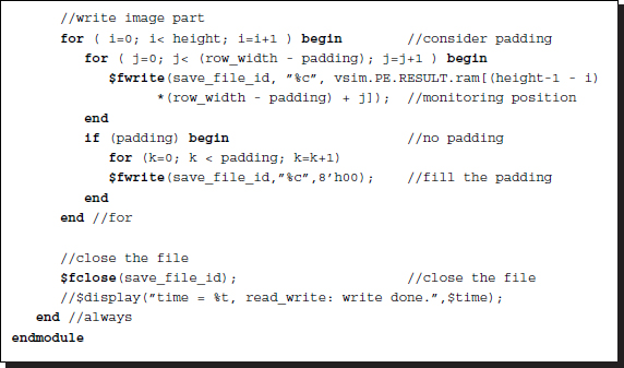
The third part of the converter writes the internally stored binary map, extracted or synthesized, to a binary file or a bmp file. For the bmp output, the internal binary file and the header must be used to synthesize a bmp file.
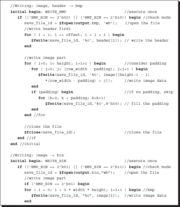
Listing 4.3 Converter: writing file (3/3)
The header may be extracted or synthesized, as explained above. Further, the binary file may be extracted or directly inputted. The bin output does not require a header as it is just a file output of the internal binary data. In this case, image size header information is not used. This processing may be needed when the bin image is provided to other image processing software to conduct preprocessing or post-processing for the simulator.
One can easily verify the correctness of the converter by transforming twice – bmp to bin and then bin to bmp. To test the design, small size images may be needed because large size images require too much time, both for simulation and synthesis.
4.3 Line-based Vision Simulator Principle
The line-based vision simulator conducts processing on a line-by-line basis. To derive such a system, we first of all need to specify the computational scheme for dealing with a frame. Let us define basic quantities and order of computation, as depicted in Figure 4.4. A frame is an image plane, defined as ![]() . The frame rate may be the conventional 30 fps (frames per second), but may be faster or slower, depending on the situation. Inside each frame, we define a strip (block, window, or lines), S(j) = {(x, j + b)|x ∈ [0, N − 1], b ∈ [0, h − 1]}, where j ∈ [0, M − h]. The strip moves downwards from j = 0 to j = M − h and returns to the top of the image, and periodically repeats this movement. In a one-pass algorithm, all computations must be completed during one scan. In a multi-pass algorithm, the computations must be repeated many times. The computational unit may be an entire strip or a smaller window (or block) in a strip. A window is defined by w(i, j) = {(i + a, j + b)|a ∈ [0, w − 1], j ∈ [0, h − 1]}, which moves to the right inside a strip. The computational unit may be the window – in which case all the pixels in the window are determined concurrently – or the pixels in the window – in which case all the pixels in the window are determined serially.
. The frame rate may be the conventional 30 fps (frames per second), but may be faster or slower, depending on the situation. Inside each frame, we define a strip (block, window, or lines), S(j) = {(x, j + b)|x ∈ [0, N − 1], b ∈ [0, h − 1]}, where j ∈ [0, M − h]. The strip moves downwards from j = 0 to j = M − h and returns to the top of the image, and periodically repeats this movement. In a one-pass algorithm, all computations must be completed during one scan. In a multi-pass algorithm, the computations must be repeated many times. The computational unit may be an entire strip or a smaller window (or block) in a strip. A window is defined by w(i, j) = {(i + a, j + b)|a ∈ [0, w − 1], j ∈ [0, h − 1]}, which moves to the right inside a strip. The computational unit may be the window – in which case all the pixels in the window are determined concurrently – or the pixels in the window – in which case all the pixels in the window are determined serially.
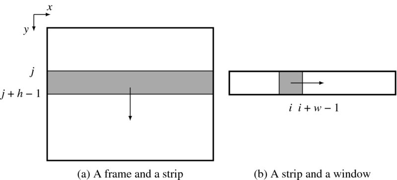
Figure 4.4 Frame, strip, and window
The overall structure of the vision simulator (i.e. the line-based vision simulation (LVSIM)) is shown in Figure 4.5. First of all, the target design is the processing element (PE), which is to be tested functionally and later synthesized for chip implementation. This processing element combines with other elements to construct the simulator. The simulator consists of three parts: a pair of image files, an input-output (IO) module, and one processor (PE) module. Generally, the images are a set of image pairs, captured from stereo cameras. However, for mono camera or motion estimation, only one set of images may be used.

Figure 4.5 The structure of LVSIM
In the forward pass, the file converter reads in two image files, converts them into binary files, and writes the results into the RAMs (IMAGE1 and IMAGE2). This action occurs repeatedly at predetermined intervals, which can be adjusted as needed. In the backward pass, the converter reads the RAM (RESULT) in the processing element, again periodically, and converts the contents to a BMP file. In this manner, a snapshot of the RAM contents can be obtained at desired intervals. The observation positions and intervals are all adjustable.
The processing element (PE) consists of three identical RAMs and a processor (PROC). Two of the three RAMs are used to capture the images from video cameras, in a real-time system. Depending on the given conditions on video input and RAMs (i.e. SRAM, SDRAM, etc.), the RAM module must be modified, using library modules, so that the image from the camera can be correctly delivered into the RAMs. For generality, this simulator uses conventional dual port synchronous RAM, instead of specialized RAM. The remaining RAM is used to store the processed result. The processor (PROC) is the main engine that actually executes the image processing algorithms. It takes a window of image from each RAM, stores the pair of image windows in two arrays, and uses them to update another array, which stores the temporary result. The windowed images are small but the resultant image is full. For a small application, the buffer, res, can also be made small like img1 and img2. The intention is to compute line by line, in a raster scan manner. The size of the strip is defined by the parameters in the Verilog head file. We will build the processing element for DP-based algorithms based on this simulator in coming chapters.
4.4 LVSIM Top Module
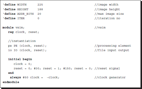
Let us now actualize the simulator concepts in Verilog HDL codes. The overall system consists of two parts: a top module (vsim.v) for simulation and another top module (pe.v) for synthesis.
The first part is the top module of the simulator, containing all the components in Figure 4.5.
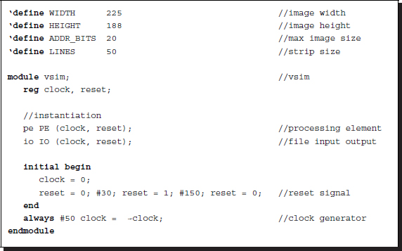
Listing 4.4 Top module for simulation: vsim.v
The parameters specify all the information necessary for synthesis and simulation. The four parameters are the size of the image (WIDTH and HEIGHT), address bits (ADDR_BITS) for the RAMs to store the images, and the number of lines (LINES) for neighborhood processing. Other parameters are written in the simulation module, vsim.v. By default, the system is tuned to the most general case: stereo and motion. Other systems, such as mono camera, stereo, or motion, can be obtained by removing some of the resources, such as RAMs and internal buffers.
This module performs three tasks: instantiation of the processing element and the input-output element, generation of a reset signal, and generation of a common clock. The input-output element is for simulation and the processing element is for synthesis. Note that there is no port communication between the two modules. The input-output element, being a simulator, uses many unsynthesizable Verilog constructs, which provide powerful tools for simulation.
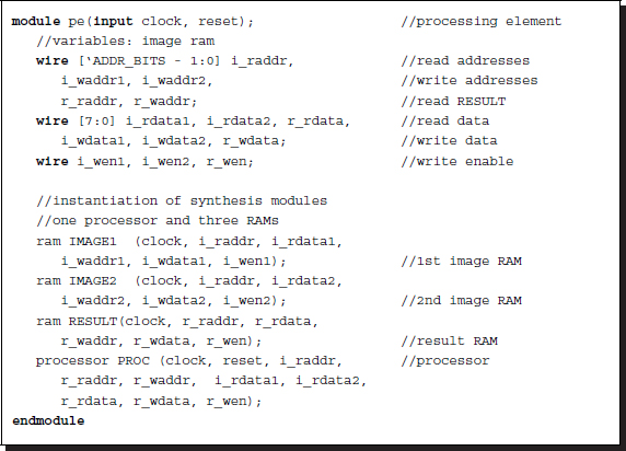
The processing element (pe.v) has the following structures:
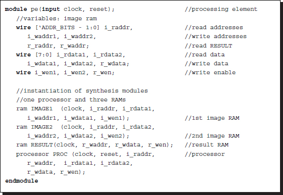
Listing 4.5 Top module for synthesis: pe.v
The purpose of this module is to create three RAMs (IMAGE1, IMAGE2, and RESULT) and a processor (PROC) and connect them, following the structure in Figure 4.5.
After synthesizing the processor (by Altera Quartus or Xilinx ISE), we can investigate the designed circuits in detail with the help of the schematic diagram. The top level view is depicted in Figure 4.6. The three RAMs and the processor are connected via address bus, data bus, and write enable signals. Although all the possible lines are connected, the connections that are utilized depend on the algorithm running inside the processor. The input signals are just the clock and reset signals. The two RAMs (IMAGE1 and IMAGE2) must be linked to the video camera, via writing ports, in an actual system. (The processor only reads from the two image RAMs it does not write to them.)
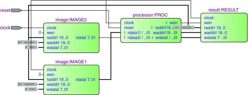
Figure 4.6 The top level schematic of the processing element
The following sections address the substructures of the simulator: memories (IMAGE1, IMAGE2, and RESULT) and processor (PROC), in detail, with working codes.
4.5 LVSIM IO System
The simulator must supply data to the processor and display the data in the various parts, including inputs and outputs, dynamically. Unlike an ordinary test bench, the vision simulator must show us data by means of images. The input and output (IO) function is based on the image converter, as explained above, but is optimized for the simulator.
The function of this module can be explained using state diagrams (Figure 4.7). The interval at which the image RAMs are fed is based on the image processing algorithm. When a frame is completed, a new frame must be available in the RAM. This instance can be obtained from a variable in the processor. An N × M image frame is defined by I = {I(i, j)|i ∈ [0, M − 1], j ∈ [0, N − 1])}. In this frame, a window is defined by W(i) = {I(i + k, j)|k ∈ [0, m − 1], j ∈ [0, N − 1]} and proceeds in the order, i = 0, 1, …, M − m + 1, where m is the number of lines in the window. When the window arrives, W(M − m + 1), it returns again to the top of the image, W(0). At this point, a new image frame must be available in the RAM. In Figure 4.7(a), the process begins when the new frame signal is detected. First, the input image files are opened and read into buffers. Next, the contents in the buffers are classified into headers and binary images. The headers are used when the output from the processor is viewed as a bitmap. The binary data is then loaded into RAM, which completes the cycle.
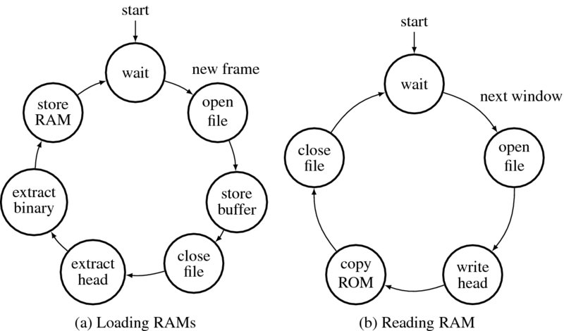
Figure 4.7 Loading RAM and reading RAM
The corresponding code reads as follows. The first part of the code is designed for loading the RAMs with binary images. In a real system, this section is replaced with video cameras that load the RAMs with binary images in effectively the same way.
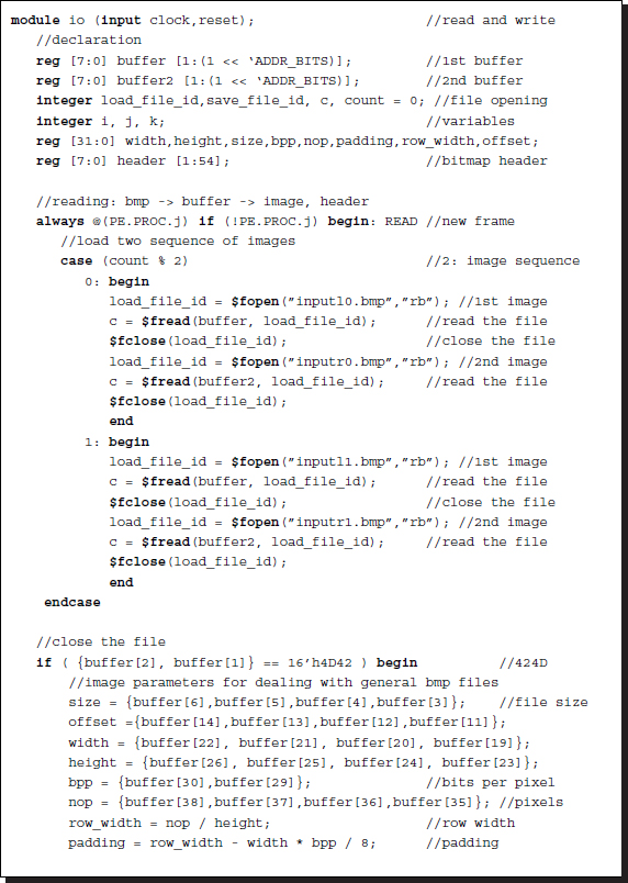
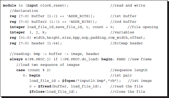
Listing 4.6 IO system: io.v (1/2)
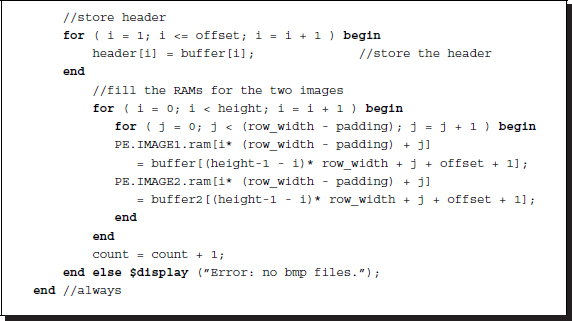
The two 2D array buffers and the 1D array are provided for two files and a header. The process waits until a new frame is needed by the processor. (This happens when the strip returns to the top of the frame in Figure 4.4; that is, S(j) becomes S(0). All the computation must be finished before a new frame arrives.) Entering the loop, the process opens two files (one file in the case of mono processing) and stores them in two buffers. From the buffers, the headers and binaries are extracted and inverted in the correct row order. The header, which is common to both images, is stored for later use, and the binaries are loaded into the two RAMs. Thus, this action simulates video cameras feeding two RAMs. For each channel, the input images are a set of bitmap files, I(0), I(1), …, I(n − 1), for n number of images. The two channels read the image sequences, synchronize, and cycle through, as indicated by the counter. This part of the code can be easily modified for different scenarios: a still camera, a video camera, two still cameras, or two video cameras. The default setting is for two video cameras.
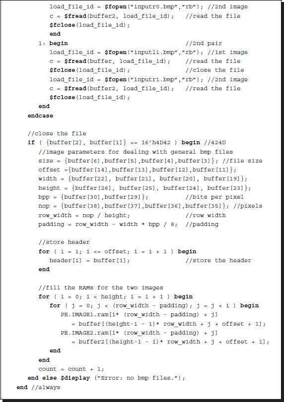
The second part of the code is designed for writing files using the data in the RAM, where the result is stored by the processor.
Listing 4.7 IO system: io.v (2/2)
The purpose of this code is to observe the result by reading the result RAM. A suitable instance for observation occurs at the point when the strip moves to the next position (in Figure 4.4, at the point when S(j) changes to S(j + 1)). The position of the observation is the result RAM, containing updated results. During the testing, it is very important to observe various places in the system. In such cases, the monitoring position can be set to the desired data in the processing element. The typical monitoring positions are the RAMs (IMG1 and IMG2) and the buffers (img1, img2, and res).
4.6 LVSIM RAM and Processor
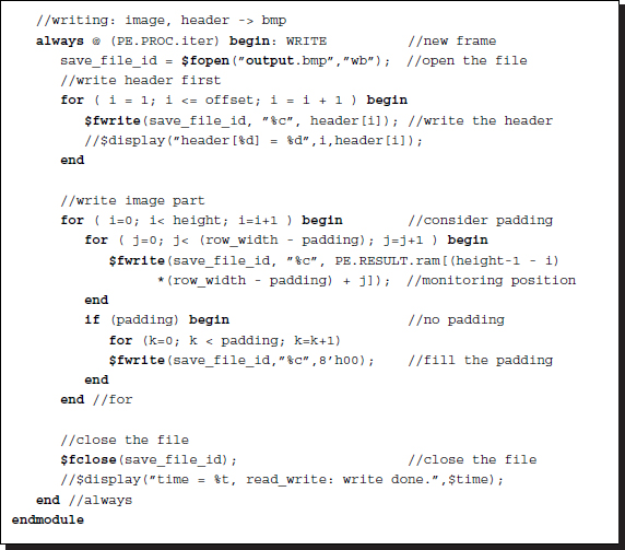
The simulator needs three RAMs, two to capture the input images (IMAGE1 and IMAGE2) and one to preserve the results from the processor (RESULT). They are all the same type of RAMs, double-port synchronous RAMs.
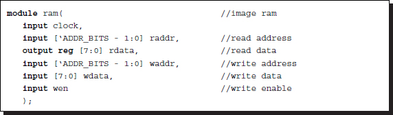
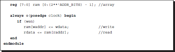
Listing 4.8 RAM: ram.v
The output is not buffered, is thus available at all times, and needs no clock synchronization. The RAM design can be aided by the templates and IPs. In an actual system, SDRAMs may be used to capture the video signals. In such a case, IPs are required for designing DRAM controllers and PLLs.
The main part of the simulator is the processor, where all the data is processed. Conceptually, the operation is defined by
where T( · ) denotes a transformation, representing an algorithm. Inputs S1(j) and S2(j) are strips of the image frames. Input S(j) is the strip from the internal array and operates like a state memory (Figure 4.8). The registers (img1 and img2) storing the strips, S1(j) and S2(j), operate as caches and copy only the required portions of the external RAMs (IMAGE1 and IMAGE2). The array (res) is a full frame memory that stores the updated states and copies them back to the external RAM (RESULT) on a regular basis. This computational structure fundamentally realizes a state machine that updates its state based on its inputs and its previous state. The general computational structure opens up the possibility for iteration and neighborhood operations, T( · ), which we will develop in subsequent chapters. Once the state, S(j), is updated, the computation proceeds to the next strip, S(j + 1). If S(j) hits the bottom of the frame, the computation advances to S(0) in the next image frame.
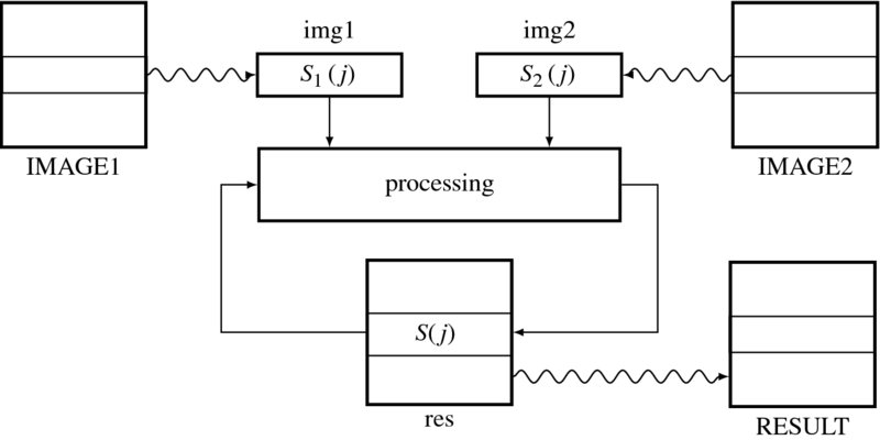
Figure 4.8 The operations in the processor
To realize this concept in Verilog HDL, we need three always blocks: reading, writing, and processing (Figure 4.9). Activated by a semaphore (do_load), the reading block reads the external RAMs (IMAGE1 and IMAGE2) and builds S1(j) and S2(j) in the internal arrays (img1 and img2). It then activates the processing block by means of a semaphore (do_ip). The processing block computes a given algorithm on S1(j) and S2(j), to update S(j) in the internal array (res). On completion, the process returns to the reading block from the processing block via a semaphore (do_load). It is not known in advance how much time the processing block may require, and so handshake control must be used for flexible control flow. On the writing side, the writing block writes the internal array (res) to the external RAM (RESULT). The two memories are the same in size and thus copying is simple. This copy operation is also relatively free from other blocks and can thus be assigned any time and interval. In the diagram, the writing action begins at the same time as the processing block begins processing.
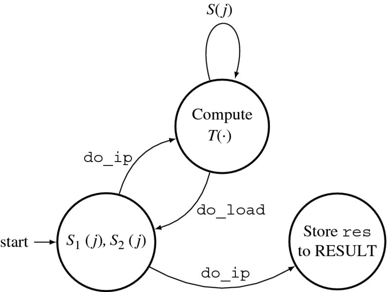
Figure 4.9 The always blocks for the processor
This scheme is general because various algorithms can be plugged into the processing block, especially algorithms involving line-based processing. In any case, the purpose of the simulator is to provide a template for the processor by using other parts intact, or with minor modifications. Detailed coding for the processing block is possible only when an algorithm is determined. The time constraint is flexible and the computational resources, S1(j), S2(j) and S(j), are enough for line-based algorithms.
The actual Verilog code is as follows.
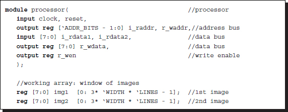
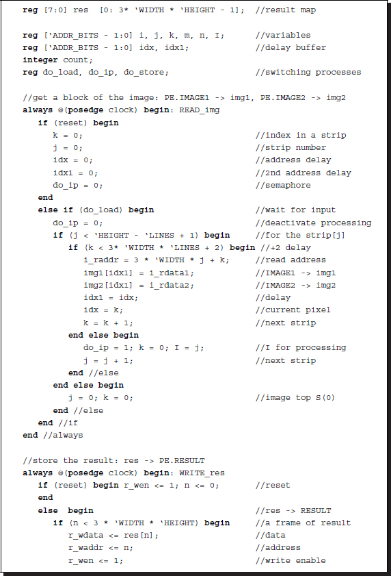

Listing 4.9 Processor: processor.v
The three always blocks appear in the following order: reading, writing, and processing. The reading block is active only when the processing block activates it by sending a semaphore (do_load). This block then begins by inhibiting the processing block using a semaphore (do_ip). Its major function is to provide new strips, S1(j) and S2(j), by copying the contents from the external memories to the internal registers. The loop count must be corrected by adding one or two more delays as ‘if (k < 3* `WIDTH * `LINES + 2),’ otherwise, the last one or two pieces of data may be ignored while they are being carried on the bus. The instances for moving to the next strip and next frame can be captured by the variables in this block. When the operations are finished, the reading block activates the processing block using a semaphore (do_ip). The processing block, when activated, begins by deactivating the reading block using a semaphore (do_load). This handshake must be carefully designed so that the semaphores are not driven by more than one always block. The writing block is activated at the same time as the processing block but can be modified to activate at any other time, for example when we want to observe the intermediate states.
4.7 Frame-based Vision Simulator Principle
The core concept of the line-based simulator is the internal cache memory, which stores only several lines of an image frame. There are many variations on this simulator. Among them, we may improve the strip so that it shifts downwards and skips more than one line. Another major improvement may be to replace the fixed cache memory with barrel shifters, in which case each line of image would be read only once. The pitfall is that computing the coordinates in a strip would be rather complicated. The line-based simulator requires less internal memory and is thus faster in general. A suitable algorithm is DP, which computes line by line. The difficulty of this simulator is the neighborhood operation in the vertical direction. Because the scope is limited to small lines in the window, the pixels at the top and bottom of the strip cannot access the neighborhood pixels. If the neighborhood size is large, this problem gets even worse. Therefore, we would have to devise a very sophisticated scheme to resolve the start of the strip and the neighborhood pixels out of the window.
The other scheme is to use full frames instead of the small windows. The internal memory would increase in this case but would facilitate the most important algorithms: neighborhood operation and iteration. In fact, this scheme may be considered as the line-based scheme with a strip expanded to a full frame. In this scheme, computing addresses for the pixels is very simple. No scheme for keeping track of starting address, as in the line-based method, is required. This scheme is suitable for algorithms such as the relaxation and BP algorithms, and so will be used a lot in subsequent chapters.
The overall structure of the frame-based vision simulator (FVSIM) is illustrated in Figure 4.10. The big difference between it and the line-based simulator is the two internal arrays (img1 and img2), which are full frame-sized, in contrast to those of the line-based simulator. Here again, the target design is the processing element (PE), which includes RAMs (IMAGE1 and IMAGE2) and a processor (PE), as shown in the figure. Thus, all the RAMs are identical in type and size. In addition, the internal arrays are all the same in size. The structure is simple and so is the address calculation. The simulator consists of three parts: a set of image files, a file converter (IO), and one processor (PE) module. As before, the images are a set of image pairs, captured from stereo cameras, without loss of generality, and thus allows mono camera or motion estimation, with one channel of the input path being activated.
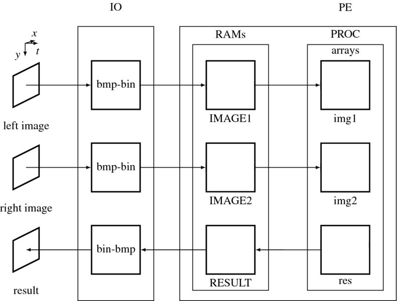
Figure 4.10 The structure of FVSIM
The IO is slightly modified so that the image can be read, and the result updated whenever the processor completes a whole frame. This scheme assumes a real-time system, in which the processor must complete the task for the current frame before the next frame arrives. This is in contrast to that of the line-based method, in which a complete processing is finished before a new line enters the internal arrays. Technically, this system needs more than one clock, one for the frame, one to read the frame into the array, and one for the processor – for consuming many clocks for each pixel. (PLL can be used to generate such clocks.) It depends on the actual algorithm to determine details of such clocks. For the observation, the contents of the RAM (RESULT) must be converted to a BMP file, on completion of each iteration.
In the following sections, we examine the components in this simulator.
4.8 FVSIM Top Module
Let us realize the frame-based simulator in Verilog HDL. Like the line-based simulator, the frame-based simulator consists of two parts: a top module (vsim.v) for simulation and a top module (pe.v) for synthesis.
The top module of the simulator contains all the modules in Figure 4.10: IO and PE. The code is as follows:
Listing 4.10 Top module for simulation: vsim.v
At the beginning, the four parameters specify all the information necessary for synthesis and simulation. The big difference is the iteration parameter, instead of the line numbers that appear in the line-based simulator. For simplicity, all the word lengths for RAMs and arrays are set to one byte, which is common in RGB bit assignment. The simulator is made even more general, including neighborhood and iteration in stereo and motion. Similar to the line-based simulator, other applications, such as mono camera, stereo only, or motion only, can be achieved by removing a channel or resources, such as RAMs and internal buffers.
This module performs three tasks: instantiation of the processing element and the input-output element, generation of a reset signal, and generation of a common clock. The input-output element is for simulation, and the processing element is for synthesis. Note that there is no port communication between the two modules. The input-output element, being a simulator, uses many unsynthesizable Verilog constructs, which facilitates powerful tools for testing and monitoring.
The processing element is the same as in Listing 4.5 but is listed here again for completeness.
Listing 4.11 Top module for synthesis: pe.v
This module consists of three RAMs (IMAGE1, IMAGE2, and RESULT) and a processor (PROC), and connects them following the structure in Figure 4.10. Incidentally, the codes are maintained with simple statements as possible for easy understanding. At the time of synthesis, the codes must be elaborated so that all the wires are terminated with drivers and all the unused variables are removed. The schematic diagram of the FVSIM is similar to Figure 4.6.
The following sections explain the infrastructures of the simulator: memories (IMAGE1, IMAGE2, and RESULT) and processor (PROC), in detail, with working codes.
4.9 FVSIM IO System
The IO function module plays a very important role in the simulator. This module must supply data to the processor and display the data in the various parts, including inputs and outputs, dynamically. Because observation of the data is important, the vision simulator must show us data by means of images. This module is a slightly modified version of that in Figure 4.7.
The function of this module can be explained using state diagrams (Figure 4.11). The intervals at which the RAM is fed is based on the image processing algorithm. When a frame has been completed, a new frame must be available in the RAM. In the frame-based simulator, this instance can be easily captured by the semaphore (do_load). In Figure 4.7(a), the process begins when the new frame signal is detected. First, the input image files are opened and read into the buffers. The contents in the buffers are then classified into headers and binary images. The heads are used when the output from the processor is viewed as a bitmap. The binary data is then loaded into the RAM, which completes the cycle.
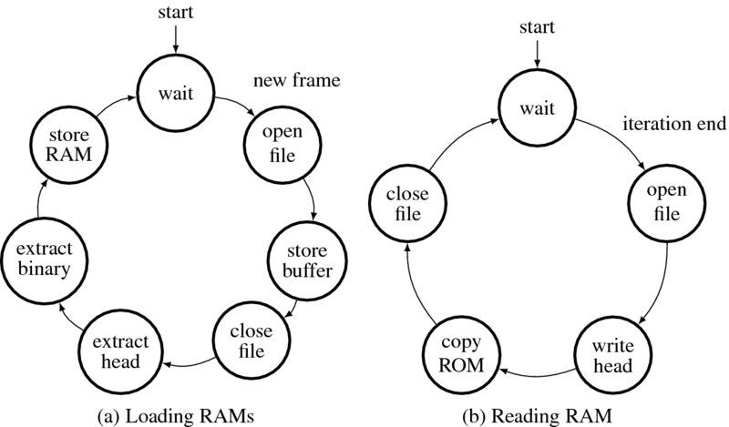
Figure 4.11 Loading RAM and reading RAM
The corresponding code reads as follows. The first part of the code is designed for loading the RAMs with binary images. In a real system, this section is replaced with video cameras that load the RAMs with binary images in the same fashion.
Listing 4.12 IO system: io.v (1/2)
The two 2D array buffers and the 1D array are provided for two files and a header. The process waits until a new frame is needed by the processor. (This happens when the strip returns to the top of the frame in Figure 4.4, i.e. S(j) becomes S(0). All the computation must be finished before a new frame arrives.) Entering the loop, the process opens two files (one file in the case of mono processing) and stores them in the two buffers. From the buffers, the headers and binaries are extracted and inverted for the correct row order. The header, which is common to both images, is stored for later use and the binaries are loaded into the two RAMs. Thus, this action simulates video cameras feeding two RAMs. For each channel, the input images are a set of bitmap files, I(0), I(1), …, I(n − 1), for n number of images. The two channels read the image sequences, synchronize, and cycle through, as indicated by the counter. This part of the code can be easily modified for different scenarios: a still camera, a video camera, two still cameras, and two video cameras. The default is for two video cameras.
The second part of the code is designed for writing files using the data in the RAM, where the result is stored by the processor.
Listing 4.13 IO system: io.v (2/2)
The purpose of this code is to observe the result by reading the result RAM. A suitable instance for observation is at the point when the internal array (res) is transferred to the external RAM at the end of each iteration. The semaphore (do_store) indicates such an instance. However, the monitoring positions and time can easily be changed to other values.
4.10 FVSIM RAM and Processor
For completeness, we repeat the RAMs here. The simulator needs three RAMs, two to capture the input images (IMAGE1 and IMAGE2) and one to preserve the results from the processor (RESULT). However, they are all the same double-port synchronous RAMs.
Listing 4.14 RAM: ram.v
The RAM design can be aided by the templates and IPs. In an actual system, SDRAMs may be used to capture the video signals.
The major difference between this and the line-based method is the processor. Conceptually, the operation is defined by
where T( · ) denotes a transformation, representing an algorithm. For each time t, the inputs, I_1(t), I_2(t), are the image inputs and S(t) is the buffer, which stores temporary results, operating as state memory (Figure 4.12). This computational structure is general and realizes a state machine, which updates its state based on its inputs and its previous state. The general computational structure opens up the possibility for iteration and neighborhood operations, T( · ), which we will develop in subsequent chapters. For a pixel, ![]() , a set of neighbors is defined as N(W(p)). Thus, the neighborhood operation is defined by
, a set of neighbors is defined as N(W(p)). Thus, the neighborhood operation is defined by
The architecture in Figure 4.12 is rather general and thus implies that this neighborhood operation is a special case. For concurrent operation, we may expand a pixel, ![]() , into a window of pixels, W(p). Consequently, the set of neighbors of the window is N(W(p)). In this case, the operation becomes
, into a window of pixels, W(p). Consequently, the set of neighbors of the window is N(W(p)). In this case, the operation becomes
We may expand this equation into iteration by introducing an iteration index, k = 0, 1, …, K − 1
To realize this concept in Verilog HDL, we need three always blocks: reading, writing, and processing (Figure 4.13) The reading block accesses the external RAMs (IMAGE1 and IMAGE2) and copies S1(j) and S2(j) into the internal arrays, img1 and img2. The reading block then activates the processing block, which computes a given algorithm on S1(j) and S2(j), to update S(j) in the internal array (res). On completion, the process returns to the reading block from the processing block. It is not known in advance how much time the processing may consume and so semaphores must be exchanged for handshake control. On the writing side, the writing block writes the internal array (res) to the external RAM (RESULT). This action is relatively free from other processing and may need long intervals. In the diagram, the writing action begins at the same time as the processing block begins.
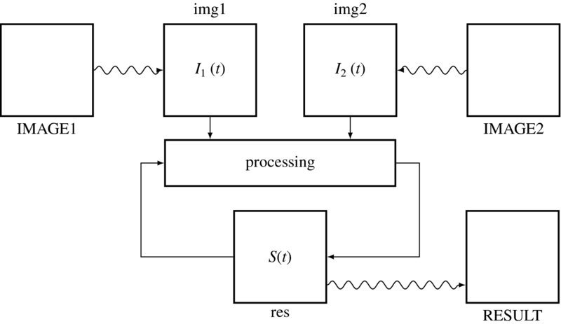
Figure 4.12 The operations in the processor
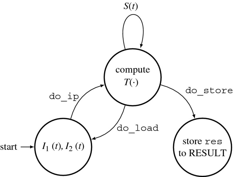
Figure 4.13 The always blocks for the processor
This scheme is general as various algorithms can be plugged into the processing block, especially algorithms involving neighborhood and iteration. The time constraint is flexible and the computational resources, S1(j), S2(j) and S(j), are enough for such algorithms.
Let us consider the actual Verilog code. The code consists of three always blocks, appearing in the following order: reading, writing, and processing. The always block for reading is as follows:
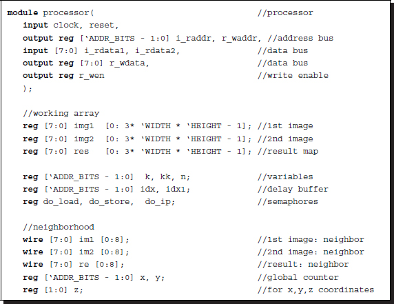
Listing 4.15 Processor: processor.v (1/3)
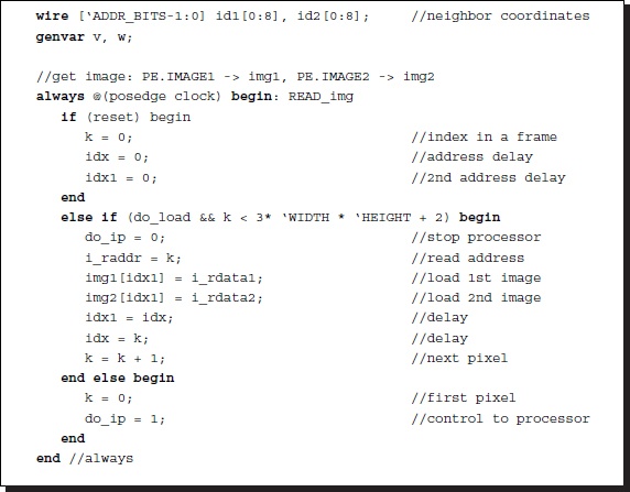
The reading block is active only when the processing block activates it by using the semaphore, do_load. This block then begins to inhibit the processing block using the semaphore, do_ip. The major operation is to provide a pair of new images, I1(t) and I2(t), by copying the contents from the external memories, RAM1 and RAM2, to the internal registers, img1 and img2. When the operation is finished, the reading block activates the processing block using the semaphore, do_ip. In return, the processing block, when activated, begins by deactivating the reading block using the semaphore, do_load. This handshake must be carefully designed so that the semaphores are not driven by more than one always block.
The writing block also does one-way processing, and continuously brings back the result to the external RAM. The writing block is activated at the same time as the reading block.
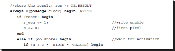
Listing 4.16 Processor: processor.v (2/3)
Therefore, the reading and writing blocks operate concurrently, without interfering with each other. The external RAM may be omitted and the resulting data can be put onto the pins, so that the data can be continuously obtained externally. It depends on the actual implementation of the RAMs and pins.
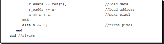
The main part of the processor consists of nested loops, with iteration outside and pixel visit in the inside loop. The always block is activated by the reading block via the semaphore, do_ip. In this manner, the always block may take as much time as needed to compute a frame, with neighborhood and iteration operations.
Listing 4.17 Processor: processor.v (3/3)
Each pixel must be accompanied by neighborhood pixels, in both images. In this code, the neighborhood calculations are achieved by combinational logic. The concept is as follows. The processor block chooses a pixel position to be computed next, which is represented by two equivalent coordinates, kk and (x,y,z). The former is the pixel counter, while the latter is a set of counters for row, column, and RGB. This way of obtaining the pixel coordinates is efficient because it avoids division and multiplication. Otherwise, we would have to compute the coordinates as ‘z = kk%3, y = ⌊kk/(3 × WIDTH)⌋,’ and ‘x = kk − 3 × WIDTH × y.’
For each pixel, neighborhood indices are computed, with boundary conditions considered. If the neighborhood is out of the boundary, then its coordinates are set to those of the center pixel. In this way, all the neighbors beyond the boundary are set to the boundary values. However, this method can be modified using reflection, resulting in the outside pixels being reflections of the inside pixels. Any other definition of the boundary condition must appear around this code. The indices are converted to the actual values of the neighbors. In addition, the corresponding neighbors on the second image are computed, using the obtained neighbors of the first image. In actuality, the definition of the corresponding pixel depends on the application. In stereo matching and optical flow, the corresponding pixel is changing dynamically and the optimal one must be searched for. This template is simply set to zero disparity or optical flow. The neighborhood definition can be expanded, so that the range of the neighborhood is beyond just one pixel. In that case too, the logic is correct but the neighborhood arrays must be expanded appropriately.
Inside the always block in the processor, the operation can be defined by the neighbor pixels from the two images and the state register, to determine a new value for the state register. In an actual application, the neighborhood and the corresponding point must be fitted to the required values, in this standard template. Finally, this computational architecture is not just for the neighborhood and iterative computation. It is a general state machine and can therefore be used in more general vision applications.
4.11 OpenCV Interface
For more general vision processing, advanced packages such as OpenCV (Baggio et al. 2012; Bradski 2002; Bradski and Kaehler 2008; Laganiére 2011) can be used in conjunction with the target architecture. The problem is that there are two levels of barriers between Verilog and C++ (Stroustrup 2013). The first barrier is the communication between Verilog and C programs. One solution is to use a buffer file at the Verilog-C boundary to transfer images and data between the two systems, as indicated above.
Now that all other parts have been introduced in terms of VSIM, we can introduce the main program, which uses OpenCV.
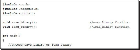
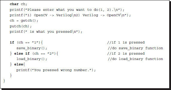
Listing 4.18 OpenCV: main
In the forward phase, the main program reads in an external file containing a set of image files, does some preprocessing with the help of OpenCV, and then writes the intermediate results to an output file, as a raw image, so that VSIM can access it. In the backward phase, the main program reads in the output file returned by the simulators, that is VSIM, does some post-processing, with the help of OpenCV, and writes the result to an output file. The advantage of using OpenCV is that the main program can access most of the image formats and convert them into the raw image and vice versa. The main program calls two procedures: one for reading in an image file into an image array and the other for writing an image array into an image file.
The reading procedure in the forward phase is as follows:
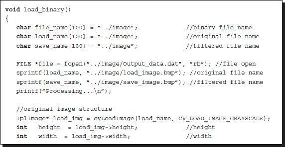
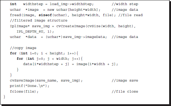
Listing 4.19 OpenCV: load_binary
The properties of the images can be adjusted by various keys that are plugged into the arguments. Moreover, all the major parameters of the image are available.
The writing procedure in the backward phase is as follows:
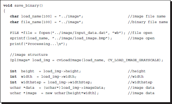
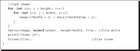
Listing 4.20 OpenCV: save_binary
The other forms of processing, such as preprocessing and post-processing, must work on the image array to generate a result as an output for either forward phase or backward phase.
To be efficient, an image processing system must comprise software and hardware systems, where the part of the algorithm characterized by serial computation with less computational complexity must be executed in software and the part characterized by parallel computation with huge computational complexity must be executed in hardware.
In this chapter, we developed two simulators, LVSIM and FVSIM, for the case of line-based and frame-based algorithms, respectively. The templates, LVSIM and FVSIM, can be expanded to the other variations. One possibility is to parallelize them by introducing nonblocking assignments. In such a case, the semaphores between always blocks must be carefully readjusted. The delay between the module and the RAM must also be considered. The other possibility is to merge the always blocks into one large finite state machine, so that the reading, writing, and processing operations are executed alternately.
In subsequent sections, we will use these simulators and focus on the processing elements. The goal is to design processing elements for the algorithms in the intermediate level vision, although some of the lower level vision is included during development. The final goal is the development of processors for stereo vision (possibly motion estimation). The purpose is not simply to derive all the codes for such systems but to introduce efficient ways of achieving our goals.
Problems
- 4.1 [Image conversion] Consider an M × N image array with RGB channels. How can you represent the image in Verilog data format? List the representations and compare and contrast their pros and cons.
- 4.2 [Image conversion] A bitmap contains a 225 × 188 image in an 8.8.8.0.0. format. What is the number of padding bytes in a row? What is the row width? What is the file size?
- 4.3 [Image conversion] Although the 1D Verilog array is useful for representing an image, sometimes it is required that the 3D coordinates (x, y, z) be retrieved from the array counter k. Let [7:0] image [0: 3 * `M * `N - 1] and [7:0] image [0:1] [0:`M - 1][0:`N - 1]. If the 1D counter k is successively incremented by one from k=0 to k=3 * `M * `N -1, how can you compute the coordinates (x, y, z) in image[z][x][y]?
- 4.4 [Image conversion] The following code is used to read and write images in three steps. First, it reads in a file in bitmap format. Next, it extracts the header part and interprets it. Then, according to the header information, it extracts the raw image and stores it together with the header information. Finally, the stored header and the stored raw image are written to an external file.
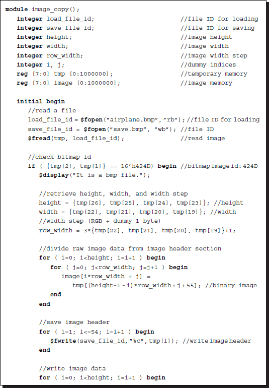
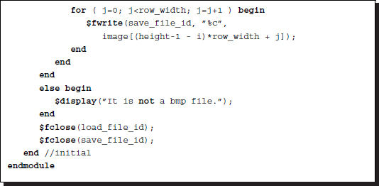
Listing 4.21 Module: image_copy.v
We would now like to enhance the code by splitting the module into two modules for reading and writing, and by building a top module that instantiates the two modules, then store the header and the raw image data in the top module by name reference.
- 4.5 [Image conversion] Let us enhance the code in the previous problem by introducing a new module, pe, which copies the raw image to another in the top module. The new module is dedicated to image processing and synthesis, while other modules are for simulation only. The current task of the processing element, pe, is just to copy one raw image into another.
- 4.6 [Simulator] In the simulator, only one place is observed in the code. How can you modify the code so that multiple places can be observed, possibly at different times?
- 4.7 [Simulator] Change the following code so that the statement is executed in each clock, instead of in one period.
- 4.8 [Simulator] What is the problem with the line-based VSIM when computing neighborhood operations?
- 4.9 [Simulator] In FVSIM, the neighborhoods out of the boundary are all assigned boundary values. In Listing 4.15, kk represents the pixel count and (x, y, z) the pixel coordinates. In many applications, the pixels around the boundary must be arranged to be mirror symmetric. For such a case, modify the given code for the mirror symmetry.
- 4.10 [Simulator] In the always block, READ_img, in Listings 4.9 and 4.15, the data from RAM was assigned to the older address. What happens if the RAM output is buffered with a register?
- 4.11 [Simulator] In the always block, READING, in Listings 4.9 and 4.15, the data from RAM was assigned to the older address. What happens if the RAM output is buffered with a register?
- 4.12 [LVSIM] Modify LVSIM using nonblocking assignments so that all the statements work concurrently.
- 4.13 [FVSIM] Make the serial implementations of FVSIM concurrent by introducing nonblocking assignments.
- 4.14 [IO] In FSIM, the internal buffers, img1, img2, and res, are filled by reading the external RAMs, RAM1, RAM2, and RES. However, the memory contents can instead be loaded quickly by the IO circuit. This method is not synthesizable but useful for quick simulation. Change io.v.
References
- Baggio DL, Emami SE, Escriva DM et al. 2012 Mastering OpenCV with Practical Computer Vision Projects. Packt Publishing.
- Bradski GR 2002 OpenCV: Examples of use and new applications in stereo, recognition and tracking Vision Interface, p. 347.
- Bradski GR and Kaehler A 2008 Learning OpenCV. O'Reilly Media, Inc.
- IEEE 2005 IEEE Standard for Verilog Hardware Description Language. IEEE.
- Laganiére R 2011 OpenCV 2 Computer Vision Application Programming Cookbook. O'Reilly Media, Inc.
- OpenCV 2013 Home page http://opencv.org (accessed May 6, 2013).
- Stroustrup B 2013 The C++ Programming Language. Pearson, Education, Inc.
- Wikipedia 2013a BMP file format http://en.wikipedia.org/wiki/BMP_file_format (accessed Nov. 16, 2013).
- Wikipedia 2013b Image file formats http://en.wikipedia.org/wiki/Image_format (accessed May 22, 2013).