
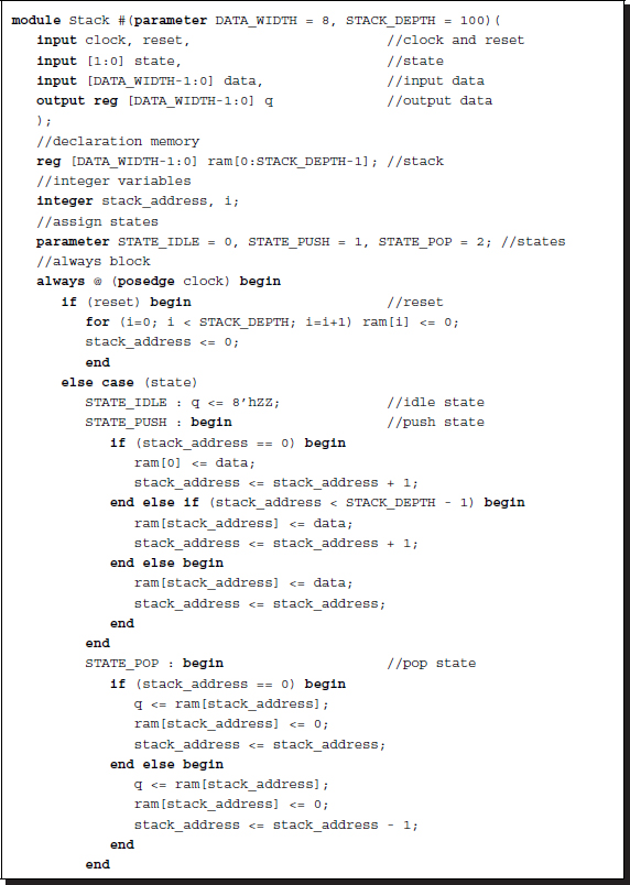
3
Processor, Memory, and Array
This chapter introduces the general structure of an image processing system and the basic architectures of its major constituents, processors, and memories.
In general, a vision algorithm can be considered as a systematic organization of small algorithms, which, in many cases, can be divided further into even smaller algorithms recursively, until the algorithms cannot be divided further into meaningful units. The final divided algorithms tend to have simple and regular computational structures and thus can be considered fundamental algorithms. We are concerned with the architectures consisting of processors and memories that correspond to the fundamental algorithms. In an ordinary architecture, the constructs are the accumulators, arithmetic circuits, counters, gates, decoders, encoders, multiplexors, flip-flops, RAMs, and ROMs. However, in image processing, the constructs are bigger units, such as the neighborhood processor, forward processor, backward processor, BP processor, DP processor, queues, stacks, and multidimensional arrays.
When considered in the algorithm hierarchy, processors and memories are located at the leaf of the tree and play the role of building blocks of the algorithms. Before we begin to design the full system, it is helpful to provide processors and memories, collectively called processing elements (PEs), that are optimally designed in parameterized libraries. We will learn how to define the processing elements and connect them in an array, allowing us to build a larger system from a set of smaller systems. This chapter discusses some processors, memories, and processor network in HDL code.
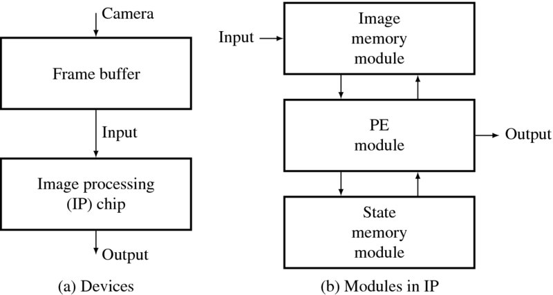
Figure 3.1 The general structure of image processing system
3.1 Image Processing System
In order to process images, possibly in real time, the hardware system must be built with at least two devices: a frame buffer connected to a camera and an image processing (IP) chip (Figure 3.1(a)). The frame buffer, or video RAM (VRAM), is a fast memory where the captured images are stored in a full frame and reading is possible when the buffer contents are being renewed. The IP chip, realized in the form of CPLD, FPGA, or ASIC, reads the images from the frame buffer, processes them according to the algorithm, and sends the results to the ports. This is a rough general configuration, and the nature of the processor and memory may vary, depending on the application.
The internal operations are represented with Verilog modules, as shown on the right side of Figure 3.1. The images in the frame buffer must be transferred to the image memory so that the PE can quickly access the image. The memory may be installed externally if the image is too large to be stored inside the chip. The PE may need additional memory, which we call state memory, to store the intermediate results and retrieve them rapidly. This memory can also be located outside if the data is too large to be stored inside the chip. The PE is the main processor that computes the main portion of the algorithm, in addition to port control such as sync and I/O signals. In a compact system, all three modules reside in the chip, while in a large system, the three modules may be located in separate chips.
We are concerned with the structure of the modules: PEs and memories. Just as there are many algorithms and architectures, there are also many PEs and memories. In an effort to determine the basic PEs and memories, we have to first investigate the nature of algorithms, as in the following section.
3.2 Taxonomy of Algorithms and Architectures
In order to derive efficient hardware systematically from the given algorithm, we need some design stages and representation schemes. Let us consider the following three stages: vision algorithm, architecture design, and HDL coding. As a starting point, the vision algorithm needs a detailed description of the computation, with statements listed in serial order. The ordinary representation is almost free, but it generally follows an Algol- or Pascal-like syntax. The architecture design attempts to interpret the algorithm in terms of hardware resources, such as PEs and memories, describing their connections and operations. At this stage, we need to specify the structure of the memory and the access points, the connections between the processor and memory, and the control mechanism, in addition to the detailed computation. The Verilog code converts the designed architecture into a behavioral description (and ultimately a circuit description). Similar to the relationship between a high-level language, assembly language, and machine code, the Verilog HDL code is converted to RTL and net-list by compilers and synthesizers. Some algorithms may be simple enough to be designed directly in the HDL coding, skipping a hardware description. However, other algorithms may need a detailed description of the hardware before moving on to HDL coding. (In this case, the hardware design paradigm is shifted to high-level synthesis, such as Altera's Vivado and Xilinx's HLS) missed.
In general, algorithms can be decomposed into smaller algorithms recursively until some well-known algorithms are reached. There are numerous well-known algorithms, such as FFT, relaxation, recursion, iteration, DP, BP, Kalman filtering, particle filtering, Bayesian filtering, graph cuts, and EM. The well-known algorithms can then be decomposed into even smaller algorithms, again recursively until the smallest algorithms are reached. The smallest algorithms are elements of the many well-known algorithms, often having no names, and thus we may call them fundamental algorithms. Examples include the neighborhood algorithm, iteration, recursion, sorting, shortest path algorithm, forward processing in the Viterbi algorithm, forward/backward processing in the hidden Markov model (HMM), inside/outside algorithm in parsing, and one-pass processing in the sum area table (SAT) algorithm (Viola and Jones 2001). (Because we cannot enumerate all such algorithms, we will focus only on the algorithms that will be used later.) The fundamental algorithms can be modeled by some architecture, which is organized by well-defined processors and memories, which we may call the fundamental architecture. The architectural description is the blueprint for the HDL coding.
In this light, we now present the algorithm hierarchy consisting of the fundamental algorithm:
- Fundamental architecture – HDL coding. Each level of description must follow this order.
- Algorithm, architecture, HDL.
Table 3.1 PEs and memories for fundamental algorithms
| Memory/Processor | a) Multi-dimensional array | b) Local register | c) Global queue | d) Local stack |
| 1) Neighborhood processor | IN algorithm GC algorithm | SAT algorithm | ||
| 2) BP processor | BP algorithm | |||
| 3) Viterbi processor | HMM, DP algorithms | |||
| 4) Forward/ backward processor | HMM algorithm |
cf. IN: iterative neighborhood, BP: belief propagation, GC: Graph cuts and SAT: sum area table.
In vision, as limited to the intermediate processing in this book, the fundamental algorithms can be decomposed into the processors and memories, as listed in Table 3.1. In this table, the top row and the left column represent memories and processors, respectively. The processors are the devices that execute the most basic operations. The memories are the devices that store temporary, input, and output data. The table entries are a few examples of fundamental algorithms, which may consist of more than one processor and memory. They may also need some other processors and memories, which are omitted from this table due to lack of regular and well-defined structures. For example, the HMM can be realized with the Viterbi processor for solving the decoding problem, and the forward/backward processor for solving the evaluation and learning problems. The DP can be realized with the Viterbi processor.
The neighborhood processor executes neighborhood operations regardless of the definition of the neighborhood and internal operation. Thus, the neighborhood processor includes a general processor that receives an arbitrary number of inputs, such as a pixel for pixel processing or a window of pixels for concurrent processing. The IN and SAT algorithms use this type of processor. The BP processor is the main processor in the BP algorithm; it receives neighbor values and emits output values to the neighbors. The forward/backward processor provides the values for evaluation and learning in HMM. The Viterbi processor finds the shortest path in the Viterbi algorithm, which is used in DP and HMM. The processors may be decomposed into smaller units, but at some point, the meaning of the processor may be lost because the remaining operations are purely mathematical and logical.
As data structures, memories can be classified as arrays, registers, queues, and stacks. An array is a data structure in which the data can be accessed randomly and be used to store intermediate results of the neighborhood. A register symbolizes small data, such as variables, reg type, and parameters, that are stored inside a processor. A queue is a data structure mostly used in one-pass algorithms, such as SAT, as we shall see later. A stack is another data structure for storing pointers in the Viterbi algorithm. On the device side, memories can be implemented in many different ways. First, they may be provided inside or outside the chip. Next, memories can be realized with various devices, such as SRAM, SDRAM, or EEPROM. A detailed specification of the target device and memory is needed at the time of synthesis.
In the following sections, we will design some essential processors and memories and provide code templates.
3.3 Neighborhood Processor
Processors are the main engine where most operations occur for updating system states. In neighborhood processing, the two major related algorithms are the iterative neighborhood (IN) and SAT algorithms. The IN algorithm receives four or eight neighbor values, updates the pixel values, and sends out the value to its neighbors, repeating this process until convergence. We can replace a pixel with a window to represent concurrent processing. This kind of operation is typical in many image processing systems, such as filtering, morphological processing, and relaxation. The SAT algorithm is an abstraction of the SAT algorithm for pattern recognition (Crow 1984; Tapia 2011; Viola and Jones 2001). It receives the values of three neighbors, updates the pixel value, and stores it until a later computation recalls it.
The neighborhood processor executes one of the basic operations, a local operation, which determines the attribute of a pixel based on neighborhood values. The obtained value is again used by the neighbors in the next iteration. This basic operation can be considered a state machine in which a pixel's state is determined by the neighborhood states.
Let us consider an architecture for a four-neighborhood system. For a given pixel, ![]() , the typical neighborhood is the set of pixels {(x, y), (x + 1, y), (x − 1, y), (x, y − 1), (x, y + 1)}. However, for the SAT algorithm, the neighbors are the set of pixels {(x, y), (x − 1, y), (x, y − 1), (x − 1, y − 1)}. Without loss of generality, let us use the former definition.
, the typical neighborhood is the set of pixels {(x, y), (x + 1, y), (x − 1, y), (x, y − 1), (x, y + 1)}. However, for the SAT algorithm, the neighbors are the set of pixels {(x, y), (x − 1, y), (x, y − 1), (x − 1, y − 1)}. Without loss of generality, let us use the former definition.
For each pixel, ![]() , the state equation is
, the state equation is

where I( · ) is an image, Q( · ) is a state, and O( · ) is an output. T( · ) and H( · ) are the state transition and observation transformation, respectively. All the complex operations are abstracted by T( · ) and all the state memories are represented by Q( · ). The operations are repeated as needed based on the predefined number of iterations. This statement means that a processor receives data from neighbors including itself as well as the image input, updates its state, and produces an output.
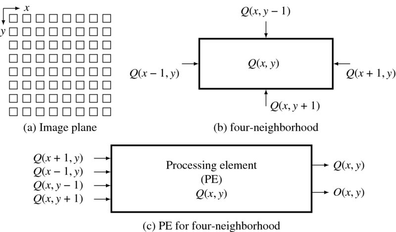
Figure 3.2 Processing elements for neighborhood computation
Figure 3.2 illustrates this concept. At the top left, there is an image plane with M × N pixels (i.e. ![]() ). PE(x, y) is defined for each pixel
). PE(x, y) is defined for each pixel ![]() that is connected with its neighbors. The four neighborhood systems are shown in the next figure. A pixel's state is determined by the image and the four neighbor states. As shown at the bottom, a PE is a system that receives inputs and produces an output. The repetition in plane
that is connected with its neighbors. The four neighborhood systems are shown in the next figure. A pixel's state is determined by the image and the four neighbor states. As shown at the bottom, a PE is a system that receives inputs and produces an output. The repetition in plane ![]() and in time can be controlled by nested loops.
and in time can be controlled by nested loops.
There are two possible approaches for the system memory. In a distributed system, each processor possesses a memory register for storing Q. A global memory scheme, on the other hand, includes a large memory unit, Q = {Q(x, y)|x ∈ [0, N − 1], y ∈ [0, M − 1]}, and all the processors access it as needed. Without loss of generality, we follow the second scheme.
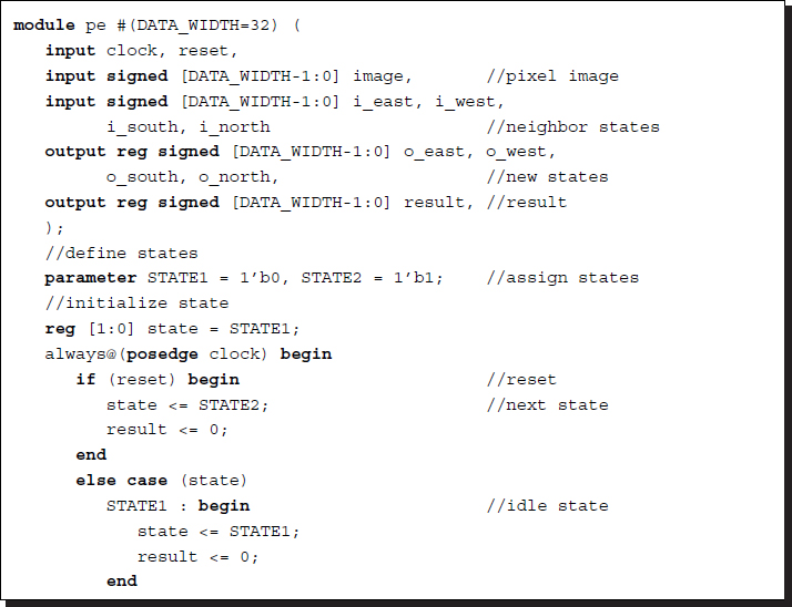
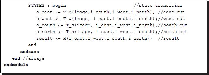
This PE can be realized by a Moore machine with two states, which can be represented by a scheme with one bit in binary coding and two bits in a one-hot coding scheme. The following code is used in the binary coding:
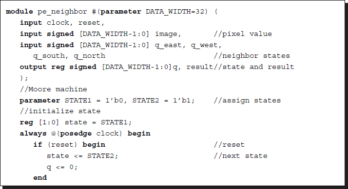
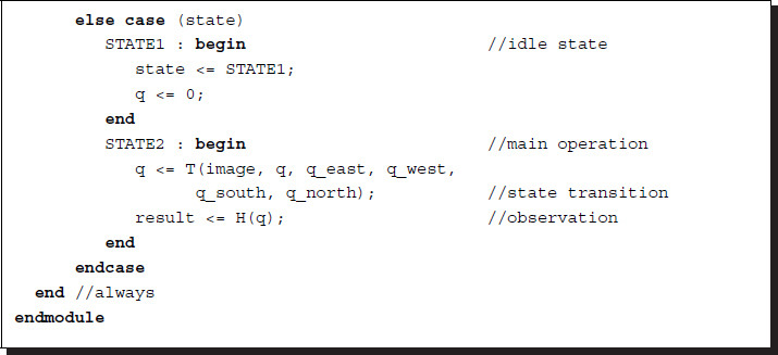
Listing 3.1 The neighborhood processor: pe_neighbor.v
In the above coding, a pixel-centered coordinate system (i.e. east, west, south, north, center) is used for convenience. Two states are used to define the idling and the main operation. State transition and output generation are written in the same block. If specified, T( · ) must be replaced with an actual code. As a whole, this processor receives five values (one pixel image and four neighborhood states) and computes the pixel state and output. To form a complete system, the processors must be connected with an external global memory (i.e. RAM) where their states are stored.
3.4 BP Processor
A more complicated type of PE can be found in BP. In this PE, the states are dependent on both input and output directions, and a different state is needed for different outputs. For a node (x, y), let us define the four states {Qe, Qw, Qs, Qn}. The corresponding state equation is described in Equation 3.2. The subscripts represent the pixel-centered coordinates – east, west, south, and north. In a simple system, the four transition functions Te, Tw, Ts, and Tn will be identical. In an actual BP system, more terms exist, such as smoothness terms (i.e. prior) that relate two nodes with costs and normalization terms that prevent overflow and underflow.
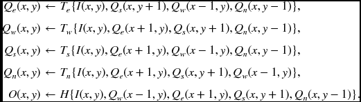
In BP, the states are called beliefs and must be updated until convergence. This operation is accomplished by iterating the image plane many times. After the convergence, all four states are used to generate the outputs, as denoted by the transformation H( · ). The operations – initialization, update scheduling, along with the state transition functions – are the major factors for designing such a system.
Figure 3.3 represents a PE. On the left figure, there is a pixel that is connected bidirectionally with its four neighbors. The right side of the figure shows the PE that receives four inputs and gives four outputs. The outputs will only be stable after the states are stabilized.
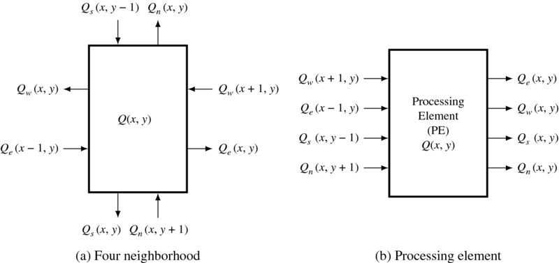
Figure 3.3 A processing element with four states
In HDL code, this processing element can be represented as follows.
Listing 3.2 The BP processor: pe.v
The operation is represented by a two-state Moore machine. The machine may start in the idle state but can jump to the normal state when it is reset. In an actual PE, the internal operation is more complicated, depending on the image input, a prior term, and a normalization factor. The image and the states may be different in data size, but for the sake of simplicity, we have made them the same here.
3.5 DP Processor
In DP and the HMM (Lawrence et al. 2007; Rabiner and Juang 1993), the Viterbi algorithm is commonly used for solving the decoding problem. Let us call the processor that is dedicated to the Viterbi algorithm the Viterbi processor. The search space consists of Nq × N nodes, where Nq is the number of states and N is the time parameter. The shortest path in this space is found via two phases: the forward processing phase and the backward processing phase. In the forward processing phase, each node determines a pointer to one of the Nq nodes and pushes it into its stack. If the parent nodes are limited to a small neighborhood around the node, then it is possible to solve this problem with a linear systolic array. Otherwise, serial processing is unavoidable because the number of connections is too large to be implemented in an array. In this case, the processor structure is very simple, like the forward processor that will be explained soon in terms of HMM. For the linear array, let us design a processor so that in later chapters we can reuse it for implementing a full DP system.
Let the position of a PE be (i, j), where j ∈ [0, Nq − 1] for states and i ∈ [0, N − 1] for image width. The PEs are connected linearly, forming an array {(i, 0), (i, 1), …, (i, Nq − 1)} for a variable i ∈ [0, N − 1]. Each PE possesses a private stack, Q = {q0, q1, …, qN − 1}, with the top being q0 and the bottom being qN − 1. During the forward processing, the PE determines the minimum cost, ϕ(i, j), and the parent index, η(i, j), which is related to the minimum cost. The costs and pointers are determined using the following equation:
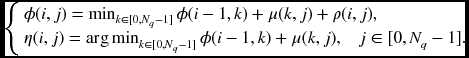
Here, μ( · ) represents a function and ρ( · ) is a local cost. A pair of neighbor processors is blocked by a register. The Nq processors on the array are all concurrent.
The corresponding circuit is shown in Figure 3.4. The left image is the linear array where the PEs are connected with neighbors via up and down links. The PEs are blocked by registers with neighbor PEs, as indicated on the edges, so that the data moves synchronously. The PE determines the cost and the pointer that is to be pushed into the stack. The function μ and the local parameter ρ are determined locally in each PE. All of the processors can update the costs and the pointers concurrently.
Figure 3.4 A linear array and the PE in forward processing
The HDL code needs an external stack that can be accessed by instantiation.
Listing 3.3 Viterbi forward processor: pe.v
To avoid exact equality, which is highly improbable, a threshold parameter epsilon is introduced. This module accesses an external stack via the value eta and the action pushpop. Each processor has its own stack. Thus, there are Nq processors and stacks. The state update operations and stack operations are concurrent for all processors.
In the backward processing phase, the PE executes completely different tasks (refer to Figure 3.5). Each PE contains a bit flag that indicates whether the node is located on the shortest path or not. To search for the shortest path, each PE must pop from the stack and, if its own flag is set to one, activate the flag in the upward or downward PE, based on the popped pointer. Since eta ∈ { − 1, 0, 1}, indicating the upward, current, and downward positions, it is easy to find the correct parent. For a flag bit b(j) at j-th PE, the new flag bit is determined by the following logic:
where η(j) is the pointer that has been popped from the stack.
Figure 3.5 A linear array and the PE in the backward processing
The HDL code is as follows:
Listing 3.4 Viterbi Backward processor: backward_processor.v
This module shares the same stack with the forward phase module. In order to access the stack, this module issues the pop command and receives the stack output.
In order to realize the Viterbi algorithm, an array of Nq processors and stacks must be activated. During the forward processing phase, the processors fill the stacks with the pointers. During the backward processing phase, the opposite actions take place. The output is popped pointers from the active processors. The pointers are relative and thus must be accumulated for the absolution position of the shortest path.
3.6 Forward and Backward Processors
In HMM, the search space is defined over the Nq × N nodes, where Nq is the number of states and N is the time parameter. In this space, the forward probability α(i, j) and the backward probability β(i, j) can be computed using the forward and backward algorithms. Given the initial values {α(0, j)|j ∈ [0, Nq − 1]} and the local measures {ρ(j, k)|j, k ∈ [0, Nq − 1]}, it is possible to compute the forward and backward probabilities:
where i = 0, 1, …, N − 1 and j ∈ [0, Nq − 1]. Here, μ(j, k) denotes the cost between the states j and k. The purpose is to obtain the result {α(N − 1, j)|j ∈ [0, Nq − 1]}. The backward probability can be obtained similarly, but in reverse time order. These algorithms are similar to the Viterbi forward algorithm, except that summation is used instead of minimum. However, unlike the Viterbi algorithm, no pointers or stacks are involved here. The memory locations are local registers.
A forward processor is shown in Figure 3.6. It is similar to the backward processor, except that the direction is reversed. The processor takes Nq inputs and produces one output. The processor cannot be implemented in a linear array, as the Viterbi processor can, because the number of inputs is too high to allow for adequate connections in an array. Instead, the computation must be executed sequentially in a double loop: j = 0, 1, …, Nq − 1 for each i = 0, 1, …, N − 1.
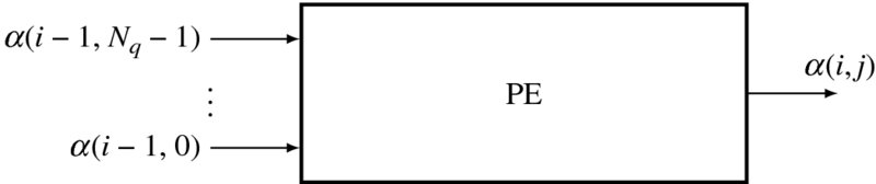
Figure 3.6 A forward processor
The processor takes Nq inputs and produces one output. The processor cannot be implemented in a linear array, as the Viterbi processor does, for there are too many inputs to be connected in an array. Instead, the computation must be executed sequentially in a double loop: j = 0, 1, …, Nq − 1 for each i = 0, 1, …, N − 1.
For a large Nq, the processor may even perform iterations in order to process Nq inputs: k = 0, 1, …, Nq − 1 for the node pair (k, j).
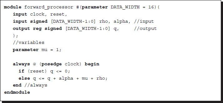
Listing 3.5 Forward processor: pe.v
For simplicity, mu is set to an arbitrary value. In addition to the processor, a RAM is needed to store Nq instances of α. Since this is a simple processor, the full computation requires three nested loops: {(i, j, k)|i = 0, 1, …, N − 1, j = 0, 1, …, Nq − 1, k = 0, 1, …, Nq − 1}. Thus, the complexity is O(NN2q). The backward processor can be coded similarly. The forward and backward algorithms can be generalized to the outside and inside algorithms (Baker 1979; Manning 2001).
3.7 Frame Buffer and Image Memory
Before proceeding further, let us first present common modules for the frame buffer and the image memory. The frame buffer must be external to the chip. For simulation purposes, the following code may be used:
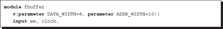
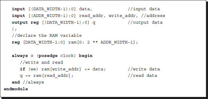
Listing 3.6 Frame buffer: fbuffer.v
This is a simple template of a dual-port RAM with a single clock, where the data can be written and read simultaneously. In one port, the video stream is written continuously, and in the other port the data is read out continuously. There are templates and libraries for advanced RAMs in most EDA tools. Initial values may be prepared with a hex editor in a binary file with a hex or mif extension.
The image memory is the workspace, in which the PE can execute the algorithm and possibly modify the contents. This memory may be designed inside the chip for a small dataset or outside the chip for a large dataset. This memory must be written to and read from concurrently. This memory can be realized by the dual-port memory as in the following template:
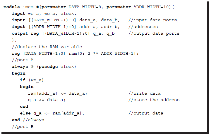
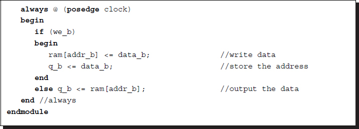
Listing 3.7 2D array: imem.v
Note that the array is written only when wena or wenb are asserted. Otherwise, the array is always read out. All of the systems that follow will use the same frame buffer module and the same image memory module.
3.8 Multidimensional Array
For the design of state memories, there are many alternative methods that depend on the available resources in a given device. The most general method is to use the standard Verilog array construct, which does not specify any available resources. A more advanced method is to use the parameterized libraries and IPs that are available in EDA tools. If the target devices, such as CPLD or FPGA, are specified, the library modules can be further tuned to the target devices. In an FPGA, there are several types of memories, such as registers, ROM, SRAM, and RAM. The registers, as portions of logical elements (LEs), are very limited in number and usage. For large memories, as required in most vision algorithms, one or more external RAMs must be connected via appropriate ports. In this section, we consider a simple design method that uses the standard Verilog construct and does not assume a particular device or commercial tool.
In image processing, the state memory is often a 2D array, Q = {q(x, y)|x ∈ [0, N − 1], y ∈ [0, M − 1]}, defined over an image plane, I = {I(x, y)|x ∈ [0, N − 1], y ∈ [0, M − 1]}. Unfortunately, the RAM is organized as a 1D array, RAM = {RAM(z)|z ∈ [0, MN − 1]}. To move from a 2D coordinate, (x, y), to a 1D coordinate, z, the address must be flattened via concatenation: z = {x, y}. Therefore, RAM({x, y}) ← q(x, y) signifies concatenation. To move from 1D to 2D, the address z must be popped to (x, y). That is, q(x, y) ← RAM({x, y}). This concept can be expanded to the case where a set of addresses must be accessed. Figure 3.7 illustrates such a memory.
The processor accesses the memory as a 2D array, but internally the memory is an ordinary 1D RAM. For accessing neighbors and a window, the address and the outputs must be a set of data, as shown on the right of Figure 3.7.
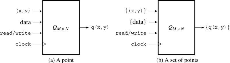
Figure 3.7 A 2D memory, Q: (x,y) for address, data for input, q for output, read, write, and clock for control and clock signals
One of the simplest RAMs is a single-port RAM having a single read/write address bus. In certain vision algorithms, the memory may be used to store the initial image values. This operation can be accomplished by initializing the contents. The following code is a template for a 2D array:
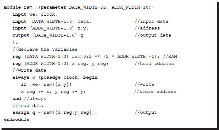
Listing 3.8 Module: ram2d.v
When synthesized, this array is actually implemented by RAM or registers. There are more advanced RAMs that have multiple ports and need multiple clocks so that reading and writing can be executed concurrently. To initialize the 2D memory, there must be an initialization process that reads the external RAM and writes to the internal 2D array.
For accessing points in a neighborhood or a window, this simple template will not work and thus must be modified to include a list of address ports. The indexed part select used in stacks can be very useful in dealing with long flat addresses.
3.9 Queue
The data structure queue (or FIFO buffer) is the main data structure in the fast relaxation equation (FRE) machine, which will be introduced in Chapter 8. The queue is special in that its size (width and depth) is constant, the data always enters from one end (i.e. the head) and leaves from the other end (i.e. the tail), a set of fixed locations are accessed concurrently, and the queue element is a window, thus forming a parallelepiped.
Let us start with a simple queue. A queue, Q, with width Nw and depth Nq is an array of Nw × Nq elements:
where q(1) and q(Nq) are the head and tail, respectively. The access addresses are the set ![]() , where Na is the number of access points. (In the FRE machine, A is a neighborhood of addresses, as we shall see in later chapters.) The output must always be available for the PE. (No loading command is needed.)
, where Na is the number of access points. (In the FRE machine, A is a neighborhood of addresses, as we shall see in later chapters.) The output must always be available for the PE. (No loading command is needed.)
A hardware queue can be considered as a system, as shown in Figure 3.8. Initially, the queue is empty. It is then filled until it is completely full. Thereafter, the queue is always full. In order to access the data in the queue, either the head or the tail address can be used as a pointer. Mathematically, for an input x, the push operation is given by
There are three techniques for implementing a hardware queue: systolic, shift register, and circular buffer. A systolic queue is a systolic array where the registers are cascaded in a linear configuration. A shift register is a register in which all data is shifted into the put operation. A circular buffer is a memory with head and tail pointers sliding along the memory buffer.
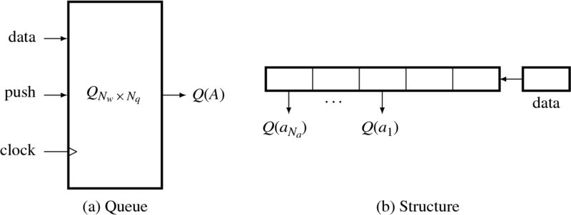
Figure 3.8 A queue Q: q for input, A for fixed addresses, Q(A) for output, shift and clock for control and clock signals
Out of these three options, we choose the shift register, which is the simplest. We design the core part of the queue using the shift register. Usually, the input data is a set of data in a window. Since the port does not allow arrays, the data must be flattened first and then it must be popped out internally. The following code illustrates this approach:
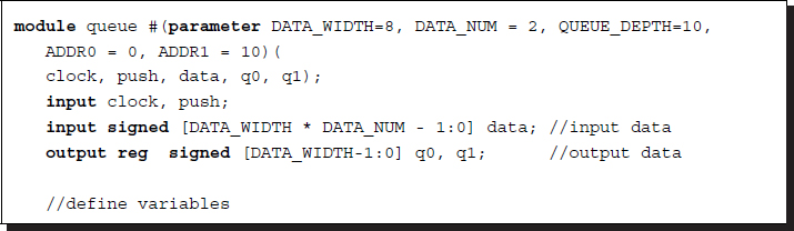
Listing 3.9 Queue: queue.v
Note the indexed part select in the data pop-out and push. The output data is a set of queue elements in a set of pre-defined positions. If the queue size is large, then it may not be possible to complete the shift operations in one clock cycle. In that case, the clock must be slowed down or counted until a block of data is pushed completely into the queue. If the queue size is large, then the circular shift buffer, which uses memory, could be used alternatively.
3.10 Stack
The stack data structure is used heavily in DP and HMM and thus must be optimized. In both algorithms, the stack is used to store a parent index and possible costs. The parent index is the node from the previous stage, which has been chosen as a parent from a set of possible options. The stack is defined by an Nw × Nq array Q = {q(1), …, q(Nq)}, where Nw is the data width and Nq is the stack depth. The stack is illustrated in Figure 3.9.
The data is an input to be pushed into the stack and q is an output to be popped from the stack. The stack is parameterized by the data width and the stack depth. The push and pop controls are coded by the state.
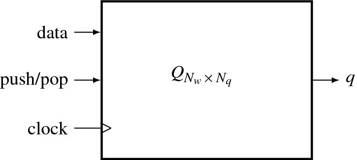
Figure 3.9 A stack Q: data for input, q for output, push, pop, and clock for control and clock signals
Listing 3.10 Stack: stack.v
The combination of various PEs and memories will result in different types of PE memory models.
3.11 Linear Systolic Array
Now, let us design a simple architecture that can execute a linear filter. Through the projects, we will learn the following concepts: designing processing elements (PEs) with state machine, designing network systems, and designing test benches. In addition, the linear pipelined array, which will be used in this chapter, is an important computational structure for DP and HMM, which is frequently used in solving computer vision problems. In later chapters, such arrays will be derived and designed for computer vision algorithms.
Once a PE is designed, a set of such elements can be connected in various ways to form different topologies. One of the possible connections is the linear arrangement, which is often called systolic array (Kung and Leiserson 1980; Petkovic 1992). The systolic arrays are very convenient for VLSI because of properties such as pipelining, nearest-neighbor connection, and identical processors. This structure is also essential for designing the DP or HMM, which will be investigated in later chapters.
As an example, let us consider a linear convolution. A signal x(t) is convolved with weights w, and the output y(t) is obtained. For a finite impulse response (FIR) filter, the system equation becomes
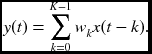
Here, K is the number of filter taps. Computationally, this simply means a weighted sum, with shifted input signals and weights.
The serial algorithm is as follows. For the sake of simplicity, we use only three taps for the filter.
Algorithm 3.1 (Serial algorithm) Compute the following:
- input: x(t).
- output: y(t).
- parameters: {w0, w1.w2}.
- for t = 0, 1, …
- y ← w0x(t) + w1x(t − 1) + w2x(t − 2) + ⋅⋅⋅ + wK − 1(t − k).
- output: y.
This can be realized with a PE. (See the problems at the end of this chapter.) However, here, we consider designing a systolic array. A given function can have many systolic arrays that are different in topology and registers. Obtaining different arrays is possible, because the registers can be redistributed by retiming (Leiserson and Saxe 1991), and the topology can be modified by topological transformation (Jeong 1984). Furthermore, interleaved circuits, which are collectively called a k-slow circuit, can be obtained by adding more registers (Leiserson and Saxe 1991). If the transformations in timing and topology are combined, numerous circuits may result (Jeong 1984).
Among the many circuits, four are shown in Figure 3.10 (Jeong 1984). Only three taps are used here, but the circuits can be easily expanded for longer taps. The numbers on the edges represent the number of registers that block the PEs. The array is shown on the left, and the PE is shown on the right. For a given array, all the PEs are performing the same operations. The data stream is permanently arranged by the fixed connections and delays. In each clock tick, all the data move in a lock-step manner, like a machine. The four circuits differ in the direction of input, output, and weight and in the number of registers. The zeroes, which are introduced between signals, represent interleaving, and independent signals can be put in those places. In (b), the weights are stored in the PEs, but the directions of input and output are opposite. In this configuration, the number of registers is reduced, but the signals must be interleaved. A set of different signals can be processed in such an interleaved system. In (c), the PE does not store weights, and thus all the signals and weights are supplied externally. The first and second arrays are dual, and thus, the third and the fourth arrays must also be dual.
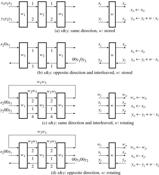
Figure 3.10 Linear systolic arrays for convolution (Numbers represent the number of registers. PEs are on the right.)
Let us design only the first array (Figure 3.10(a)). The design consists of three modules: four identical PEs, a network, and a test bench. The network module connects the four PEs in a cascaded configuration by using the output of one module as the input of the other module. The overall system is a Moore machine.
A PE consists of a weight memory, a register for the x output, and two registers for the y output. Using the memories, we express the internal operation of a PE by the hardware algorithm.
Algorithm 3.2 (PE(k)) For a PE(k), do the following:
- input: {xi(k), yi(k)}.
- memory: w(k), xo(k), {y(k), yo(k)}.
- output: {xo(k), yo(k)}.
- initialization: w(k).
- for each clock
- y = yi(k) + w(k)xi(k).
- output: xo(k)⇐x(k), yo(k)⇐y.
Here, k means the id of the PE. The Verilog procedural assignments are used – blocking (=) and nonblocking (<=), to clarify the serial and concurrent processing.
For Algorithm 3.2, we can write the module, pe.v.
Listing 3.11 Module: pe.v
In coding the PE, it is convenient to use four states: state 1 for idle state, state 2 for loading filter weights, state 3 for the weighted sum, and state 4 for output. In the idle state, a PE stays unchanged until the system is reset. Once it is reset, the system goes to state 2, where the input, which is the weight, is loaded into the internal memory. It is economical to share the input port for the weight and data input, in time-sharing – weights first and data next. When all the weights are loaded, the system goes to state 3, where a multiplication-accumulation is performed. The state then goes to 4, where the output signals are shifted into the registers. Afterward, states 3 and 4 are visited alternately until the system power is turned off.
The next stage is to define a network module that configures the PEs, connecting their outputs and inputs. The hardware algorithm is shown below.
Algorithm 3.3 (Network) Connect {PE(k)|k ∈ [0, 2]}.
- input: x.
- output: yo(2).
- for each clock tick, do the following:

In this network, the two outputs of a previous PE become the two inputs of a subsequent PE, except in the case of the first PE, which receives the two inputs from outside. The output of the last PE is the system output. Like PEs, the network is described by the connection points instead of the system clock, which is already implicit in the hardware.
For Algorithm 3.3, we can build a module, network.v.
Listing 3.12 Module: network.v
There are three methods for connecting modules in a chained topology. The first method is to enumerate all the PEs and their ports directly. The better method is to use the communication net, which is used in this example. By this method, we used two intermediate variables – t and s – to form a chained configuration. There is another method using the Verilog construct generate.
Finally, the network must be tested with a test bench, tb.v.
Listing 3.13 Module: tb.v
In the code, the network is instantiated with the name UUT, and the signals are supplied by the codes expressed thereafter. In the signal stream, simulated by the random number generator, the first four input data are used as weights, and the remaining data are used as signals. There is some latency because of the tap size, weight preparation, and other initialization processes.
The three modules tb.v, network.v, pe.v collectively construct the overall system and can be simulated. The simulated signals are shown in Figure 3.11. In the left panel, the input and output reset and clock are listed. The right panel shows the signals' corresponding nets and variables.
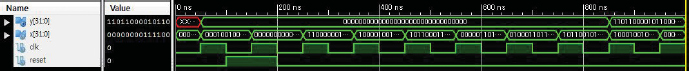
Figure 3.11 Simulation result
The synthesis tool can provide a schematic diagram, as shown in Figure 3.12. The schematic describes connections of the four PE modules. An IDE usually provides functions for observing the design in detail. Electronic design automation (EDA) tools such as Altera Quartus tools and Xilinx ISE (or Vivado) provide a complete set of tools ranging from editing to FPGA programming.
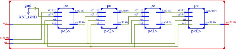
Figure 3.12 RTL schematic diagram after synthesis
Problems
- 3.1 [Neighborhood processor] Define the average with four-neighborhood and modify Listing 3.1 for the image average.
- 3.2 [Neighborhood processor] Integrate an image by modifying Listing 3.1 for the image average.
- 3.3 [Neighborhood processor] The code, Listing 3.1, is designed for a four-neighborhood system. Change the code for the eight-neighborhood system.
- 3.4 [Neighborhood processor] In Listing 3.1, the image is considered mono color. Expand the mono to the three channels, R, G, and B, all with the same word length.
- 3.5 [Viterbi processor] The purpose of the Viterbi forward probability is to find the ending of the shortest path. Write a code for finding the ending with the given {α(N − 1, j), η(j)|j ∈ [0, Nq − 1]}.
- 3.6 [Viterbi forward processor] The template, Listing 3.3, is designed for only three-neighbor. If the Nq nodes must be considered in comparing operation, the linear array is not possible due to enormous connections. In that case, serial processing is necessary. Write the code in HDL.
- 3.7 [Forward backward processor] The purpose of the forward algorithm is to compute the conditional probability that is used to solve the evaluation problem. Let the joint probability, P(X|Ψ), where X is the Markov process and Ψ is the prior. Then, write a code for computing P(X|Ψ) with alpha, which is obtained by Listing 3.5?
- 3.8 [RAM] In Listing 3.8, 1D array is used for storing image data (in the sense of word unit). Change the internal array, ‘ram,’ to a 2D array.
- 3.9 [Array] In Listing 3.5, the signal input was used to carry initial weights. Instead, the weight can be loaded from an internal memory. Change the weight setting with a reg loading in the reset block.
- 3.10 [Array] In Listing 3.6, modify the Verilog codes pe.v, network.v, and tb.v so that the number of taps can be more general.
- 3.11 [Array] In Listing 3.5, for pe.v, the state coding is done in a ‘binary scheme’. Change the state into a ‘one-hot’ scheme.
- 3.12 [Array] In Listing 3.5 to Listing 3.7, for pe.v, change the Moore machine into the Mealy machine with both binary and one-hot state representations.
- 3.13 [Array] In Listing 3.5 to Listing 3.7, for the module network.v used the ‘communication list,’ t and s are used to connect the ports of PEs. Instead of a connection list, use generate to obtain an equivalent network.
- 3.14 [Array] Design the other arrays in Figure 3.10 by modifying the following Verilog codes: pe.v, network, and tb.
- 3.15 [Array] Given the equation y(t) = w0x(t) + w1x(t) + w2x(t − 2), t = 0, 1, …, express a hardware algorithm that uses only a PE.
- 3.16 [Array] Given the equation y(t) = w0x(t) + w2x(t − 2)2, t = 0, 1, …, express a hardware algorithm that uses only a PE.
- 3.17 [Array] An IIR filter is given by y(t) =
 . Design a machine.
 - 3.18 [Array] For an image I(x, y) (x ∈ [0, N − 1], y ∈ [0, M − 1]), the first-order forward difference is defined by f(x, y) = I(x + 1, y) − I(x, y). Design a machine for this operation.
References
- Acceleware 2013 OpenCL Altera http://www.acceleware.com/opencl-altera-fpgas (accessed May 3, 2013).
- Baker J 1979 Trainable grammars for speech recognition In Speech communication papers presented at the 97th meeting of the Acoustical Society of America (ed. Wolf JJ and Klatt DH), pp. 547–550 Acoustical Society of America.
- Crow FC 1984 Summed-area tables for texture mapping Computer Graphics (SIGGRAPH '84 Proceedings), pp. 207–212. Published as Computer Graphics (SIGGRAPH '84 Proceedings), volume 18, number 3.
- Jeong H 1984 Modeling and transformation of systolic network Master's thesis Massachusetts Institute of Technology.
- Kung H and Leiserson C 1980 Algorithms for VLSI processor arrays In Introduction to VLSI Systems (ed. Mead C and Conway L) Addison-Wesley Reading, MA pp. 271–291.
- Lawrence R, Rabiner R, and Schafer R 2007 Introduction to Digital Speech Processing. Now Publishers Inc., Hanover, MA USA.
- Leiserson C and Saxe J 1991 Retiming synchronous circuitry. Algorithmica, 6(1), 5–35.
- Manning C 2001 Probabilistic linguistics and probabilistic models of natural language processing NIPS 2001 Tutorial.
- Petkovic N 1992 Systolic Parallel Processing. North Holland Publishing Co.
- Rabiner L and Juang B 1993 Fundamentals of Speech Recognition Prentice Hall signal processing series. Prentice Hall.
- Tapia E 2001 A note on the computation of high-dimensional integral images. Pattern Recognition Letters 32(2), 197–201.
- Viola P and Jones MJ 2011 Robust real time object detection Workshop on Statistical and Computational Theories of Vision.
- Xilinx 2013 High level synthesis http://www.xilinx.com/training/dsp/high-level-synthesis-with-vivado-hls.htm (accessed May 3, 2013).