You're reading the latest electronics magazine and there's an article exactly right for your latest project. The author describes a circuit that will do just what you need to finish the job! Schematics are a common feature of many articles, both on the Web and in magazines. But those are just articles — there's no kit available, not even a printed-circuit board! You can build that circuit anyway by using one of the three techniques in this chapter: dead-bug style, Manhattan style, or wire-wrap. These methods have been used for years, even decades! Ready to give it a try? Let's go!
Tip
Even if a printed-circuit board (PC board) is not available for the circuit, the author may offer a kit of parts, a programmed microprocessor, or hard-to-find special parts. Print magazines have also begun adding supplemental material on their companion Web sites.
What types of circuits are suitable for building with the techniques in this chapter? As a beginner, you should start out simple, limiting yourself to building circuits with a few ICs at most. If the circuit has digital signals, they shouldn't be faster than a few megahertz. For analog or linear circuits, avoid those that are complex, very sensitive, or for which layout is critical. Work your way up to the fancier and more difficult circuits. There is a built-in limit to this process as more complex circuitry often requires a PC board, meaning that there should be one available for you to order.
Don't forget to keep your shop notebook handy while you're working! You never know when you'll have a good idea or need to record some measurements. When you're done, be sure to document what you built for later reference. "Tomorrow" is never a good time to write things down!
What method should you choose from the three presented here? None of the three is suited for high-power designs — those that involve currents of more than an amp or two, particularly wire-wrap which can only accommodate currents of around 100 mA at most. For high-current and high-voltage circuits, stick with point-to-point techniques that use separated terminals on insulating strips.
If you want to build a simple circuit that has one or two ICs, use the dead-bug technique. If the design has a lot of discrete components, such as a transistor circuit might have, then Manhattan style is more appropriate. Complex circuits and especially digital circuits are best done with wire-wrap, but don't try high-speed digital circuits or sensitive analog circuits with critical layout or noise constraints. If you really want to compare the techniques, build one circuit using each of the methods!
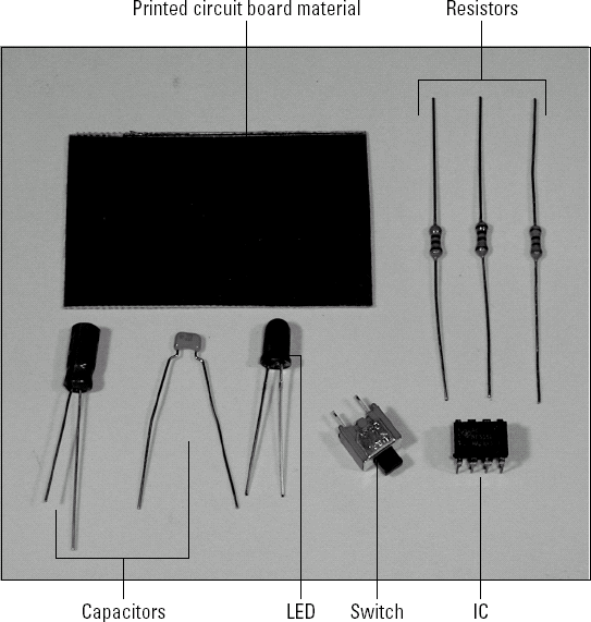
Once you've researched your circuit and developed a complete parts list, you're ready to ... get ready. Unless you have a very well-stocked shop, you're going to have to gather the necessary resources.
Develop a complete parts list, including all sockets and hardware. Make sure you have enough supplies of consumable materials such as terminals and wire before you start.
Order all required parts and obtain all necessary tools to build the circuit.
Determine the size of the PC board or wire-wrap board you'll be using.
Lay out the circuit to scale on paper first. It recommended that you use a scale of 2:1 or 4:1 so the drawing is easy to make and read.
Cut the board on which you'll build the circuit. Drill any necessary mounting holes before you begin constructing the circuit.
Make a plan of all the major steps you'll need to take, including testing.
Clean off your workspace and make sure you have all the tools and supplies that will be needed.
When the parts arrive, you'll be ready to go!
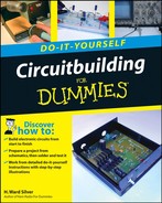
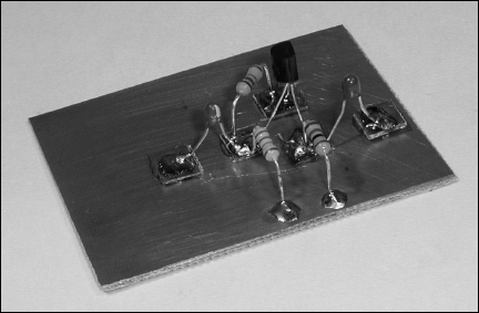
Okay, okay, I'll cut right to the obvious question. It's called dead-bug style because the ICs are all mounted upside down on the PC board with most of their legs sticking up in the air! Figure 6-1 shows why — they look like a lot of ... dead bugs! Another name for this type of construction is "air circuits" because the components are attached directly to each other over the underlying PC board. The technique is easy for beginners because it requires no special tools, gadgets, or techniques. Just solder the parts together and to a PC board and go! This is a great method to wire up a simple circuit to see how it really performs.
When building ala dead bug, the PC board surface is usually made to be the circuit's ground. This is sometimes referred to as a ground plane. Because the ground is literally everywhere and it's such a wide conductor, dead-bug construction works well for sensitive circuits and even at high frequencies. Conversely, this makes routing power supply connections a little more difficult, since everything is exposed.
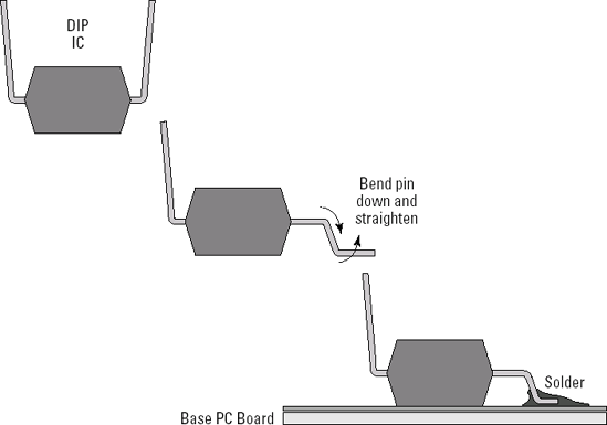
Figure 6-1. In dead-bug construction, ICs are turned on their backs with the pins extending up. Some pins may be soldered directly to the PC board surface. Most are soldered to components. Other components may also be soldered to the PC board, usually wired to be at ground voltage.
Dead-bug construction generally becomes impractical once the IC pin count exceeds 20 pins or if there are more than two or three ICs. Complex circuits have so many connections and components that it becomes hard to keep all of the connections straight and separated. Dead-bug style works best with one or two ICs.
Many of the components will attach directly to a pin of the IC (see the schematic in Figure 6-2). For this reason, the DIP ICs are greatly preferred in dead-bug construction. Surface-mount and leadless ICs (PLCC, QPCC, ball-grid array packages) are generally unsuitable for dead-bug construction.
Tip
If your circuit doesn't have a lot of components that attach to ground, you can use high-value resistors (1 MΩor higher) as supports for other components. Solder one lead of the resistor to the PC board and stand it upright. Other components can then use the remaining lead as a tie point for connections with other components. Terminal strips (metal solder lugs mounted on an insulating strip — www.abbatron.com/products/?dir=/part/get/hdw_tsb_solb) can also be used.
To make the connections, components are mostly soldered directly together, lead to lead. You will have to bend the leads and orient the components to make the circuit work electrically and for mechanical stability. If jumper wires between connections are needed, bare wire can be used for short distances, but insulated #30 wire-wrap wire (see the final task "Constructing the DC-to-DC Converter Circuit" in this chapter) or #24 or #26 hookup wire can be used. Solid wire is preferred because it will keep its shape, whereas stranded wire is more flexible.
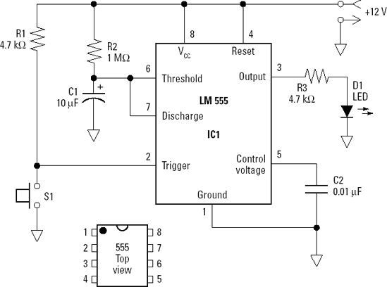
Figure 6-2. The schematic shows the configuration for a 555 timer IC to output a single positive pulse whenever switch S1 is closed. The length of the output pulse is 1.1 × R2 × C1 seconds.
When complete, a dead-bug circuit can be a real piece of sculpture. Or it can be a mess. It's up to you how it looks. Electrically, arty and messy will probably perform about the same, so it's a matter of your personal preferences how much time you spend arranging the components, whether wires are bent at right angles, and that kind of thing. My personal preference is for a neat appearance, but it takes longer.
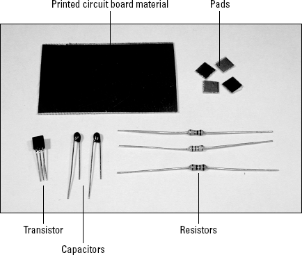
What? Another obvious question? Well, okay, this technique is called Manhattan style because small squares of PC board material are glued onto the larger piece of PC board. The small squares act as insulated tie points for soldering circuit components together. The result looks a bit like a city map with the squares representing city blocks and the space between them the streets.
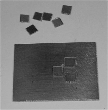
Where do the pads come from? You make them, of course! It's easy! Start by cutting a strip of PC board material about ¼" wide. (The material can be single- or double-sided.) Use the same technique for scoring and breaking the PC board as described in Chapter 5's task "Building a 12V-to-5V Regulator." Take a pair of medium-sized wire cutters, heavy scissors, or tin snips and cut the strip into small, square pieces as shown in Figure 6-3. Once you get started, it's a good idea to make a large number of pads for future use.
Figure 6-3. Cutting a strip of PC board material into small squares creates isolated pads. The pads are glued onto a base of PC board to be used as tie points for circuit connections. The "block and street" grid pattern of the pads on the base material gives rise to the name Manhattan-style construction.
While this task will use square pads — and most circuit builders do use square pads — there is no reason that they have to be square. You can use a heavy-duty hole punch to cut round pads, the pads can be rectangular, or even oddly shaped. In fact, long narrow strips make good power supply rails, just as for the solderless breadboard in Chapter 3! Take advantage of some spare time to make a couple dozen pads of different sizes and shapes, storing them in small zippered plastic bags.
Pads are usually attached in rough alignment with the circuit schematic shown below in the task "Constructing a Shortwave Buffer Circuit". It is not necessary to attach all of the pads at once, since as the circuit is built, it's often necessary to adjust the layout for convenience. When you prepare the schematic for building, go through it and outline the connection points that will use a pad to help you visualize pad placement.
Manhattan-style construction works best when the circuit is composed primarily of discrete components, such as resistors, capacitors, transistors, diodes, and so forth. If ICs are present, they aren't connected directly to the pads, but other components may be. This creates a hybrid style of Manhattan style and dead-bug style! This type of construction can be used at HF (High Frequency) with good results, even though each pad adds a little capacitance to ground.
The pad-based technique rapidly becomes untenable when you have more than 25 pads or more than a couple of ICs. Remember that this technique is not meant for mass production or for building miniaturized or complex equipment. It's a useful way to build one of something or give a new design a try when you expect to be doing some experimenting.
No mysteries exist about the reason for the name of this circuitbuilding technique! Wire-wrapping was developed in the 1960s for building telephone system equipment. It rapidly became popular for building complex circuits that needed to be modified (such as for prototypes) or that were only constructed in low volumes. Wire-wrap can even be automated, building large circuits composed of dozens of ICs on a single board! (Additional information about wire-wrapping is available in Wikipedia at http://en.wikipedia.org/wiki/Wire_wrap.)
A connection made by wire-wrapping is shown in Figure 6-4. Solid copper wire, plated with silver or some other soft, non-oxidizing metal, is tightly wrapped around a square metal pin. The corners of the pin bite into the wire very tightly, keeping the joint tight. Without some kind of strain relief, the sharp bend around the pin's edge would cause the solid wire to eventually crack. To cushion the wire, one or two turns of the insulated portion of the wire are first wrapped around the pin at the bottom of the wrap.
Because the connections are made with insulated wire, the ICs in the circuit can be very close together. The wires connecting their pins are routed along the rows between them. This allows for very densely packed circuits, just right for digital logic and microprocessors.
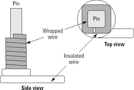
Figure 6-4. Wire-wrapping is a method of building circuits without soldering. A solid copper wire is wrapped tightly around a square pin whose edges bite into the wire for a secure connection. A turn or two of insulated wire at the bottom of the wrap provides strain relief for the wire.
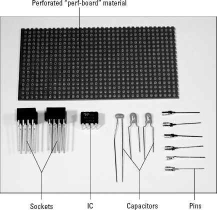
Wire-wrapping requires special tools and wire as shown in Figures 6-5 and 6-6. Besides some kind of wire-stripping tool or a combination stripping/wrapping/unwrapping tool, you'll also need wire-wrap sockets with long pins that extend through an insulating board. You'll mount discrete components such as resistors and capacitors to a socket header or wire-wrap pins before plugging it into a socket. A must-have material is perfboard made of an insulating plastic or resin material and drilled with a grid of holes 0.1" apart. Figure 6-5 shows wire-wrap labels that slip over the socket's pins, holding the socket to the board and labeling each pin by number. Next to the pin label is a pair of pins that can be pressed into the perfboard and used to connect to individual wires or components. Most of the wire-wrapping you will do uses these tools and materials.
Figure 6-6 shows a motorized wrapping tool. Most circuits can be made using the manual combination tool shown in Figure 6-5. If you do a lot of wire-wrapping, however, you'll definitely want to purchase the motorized wrapper. It makes a complete wrap in less than a second!
The wire used for wire-wrapping is not ordinary solid hookup wire. The wire itself is a specific size: #30. Most stripping and wrapping tools are designed to work with this standard size. The wire is also coated with silver or some other soft metal that will make a good connection with the sharp edges of the wire-wrapping pins. If you use bare copper wire, for example, the connections will eventually degrade and the circuit won't work properly. The insulation, called Kynar®, is formulated to break cleanly and evenly when stripped from the wire. Use wire-wrapping wire to avoid a lot of unnecessary headaches.
Pin labels come in various sizes to fit all of the common socket sizes; from 6-pin to 64-pin. Using a pin label to hold the socket against the board until a wire or two has been attached allows you to avoid using glue. While you can use a cyanoacrylate "super" glue, you don't want to get any glue on the pins as you slide the socket onto the board; this can cause bad connections that are hard to find. The label will hold the socket firmly enough to keep sockets seated firmly against the back of the perfboard.
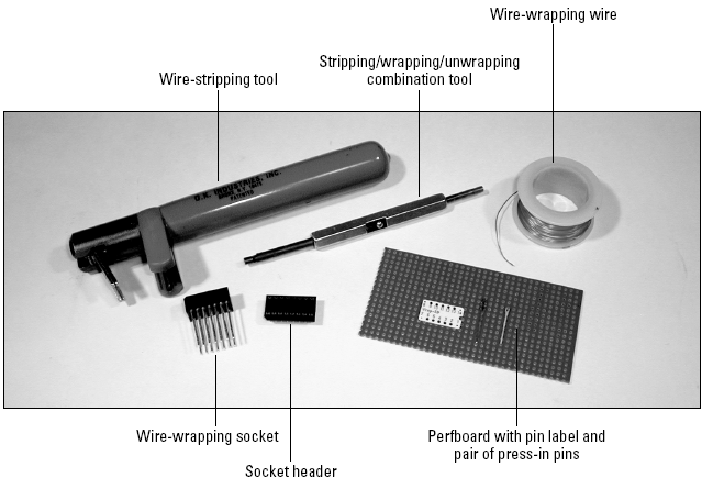
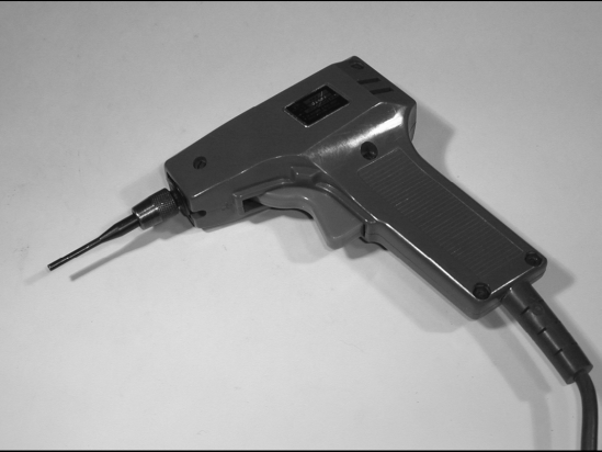
Figure 6-6. A motorized wrapping tool saves a great deal of effort when constructing complex circuits or if you will do a lot of wire-wrapping.
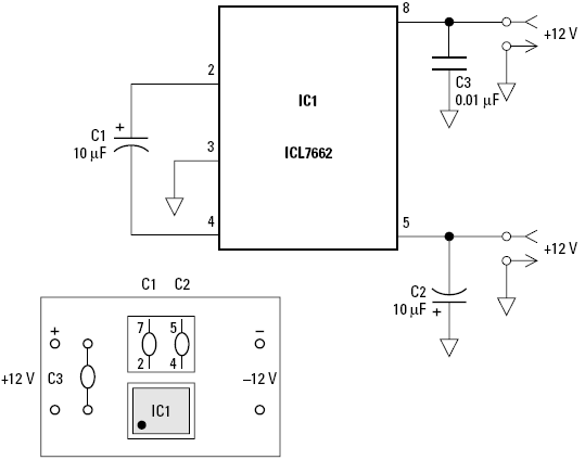
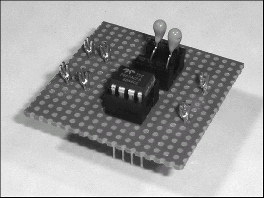
Later in this chapter, you will build a simple DC-to-DC converter circuit. The star of this circuit (shown in Figure 6-7) is the ICL7662 IC. It contains the necessary switches and clock signals to perform the electronic sleight-of-hand that creates the negative voltage. This particular circuit uses four of those switches. The chip first connects C1 to the +12V input and ground, charging it up to +12V. Those connections are opened, leaving the capacitor full of charge, but not connected to anything. The positive terminal of C1 is then connected to ground and its negative terminal to pin 5. Some of the charge stored in C1 is then transferred to C2, but with the opposite polarity from the input power. Then connections are opened and the process is repeated, just as if a bucket (C1) was being used to carry charge from a tap (the input power) to a tank (the output capacitor, C2).
The ICL7662 does this so quickly (each step takes only about 10 μs!) that to the circuit being supplied with negative voltage, it looks like a regular power supply is connected. The only limit on output current that can be generated is from the size of the capacitors and the speed at which the chip works. The ICL7662 can do several other neat tricks, too. Download its data sheet from www.datasheetcatalog.com/datasheets_pdf/I/C/L/7/ICL7662.shtml to learn about this interesting device.
This circuit uses one of the most popular ICs of all time, the 555 timer. There is a good description of how this circuit works at www.uoguelph.ca/~antoon/gadgets/555/555.html or at en.wikipedia.org/wiki/NE555. This simple IC can be wired up to output single pulses, a continuous stream of pulses, act as a time delay, and perform many other functions its designers never imagined. Still going strong after more than 30 years of life, the 555 timer should be a part of every electronic-er's bag of tricks!
In this example circuit, the timer is wired to output a single pulse whenever the reset switch is closed. This is the monostable configuration. The length of the pulse is determined by the values of C1 and R2. The output of the timer (pin 3) will be ON — at the power supply voltage (VCC) — as long as the voltage on C1 is less than 2/3 VCC. Assuming the switch is closed just long enough to discharge C1, the output will be 1.1 × R2 × C1 seconds long. The LED will light whenever pin 3 is ON. With R2 = 1 MΩ and C = 10 μF, the duration of the pulse should be about 11 seconds.
Start by making a photocopy of the schematic and making sure you have all the parts ready to go.
Tip
Use a fine (small-tipped) pair of needle-nose pliers. The larger needle-nose pliers are more suited to mechanical chores and are too coarse for the job at hand.
Cut and clean a rectangle of PC board material about 1 ½" square, as shown in the task "Constructing the Regulator" in Chapter 5. Size is not critical; it's better to have the board be a little too large than too small. You can use either single-sided or double-sided PC board. Cut the board by scoring it with a metal straightedge and sharp utility knife. Score the board on both sides and then bend it over the edge of your workspace or in the small vise.
Use the pliers to bend Pin 1 of the IC, as shown in Figure 6-1 earlier in this chapter. Solder Pin 1 to the PC board (ground). Mark off each connection on your schematic as you create the connection on the board.
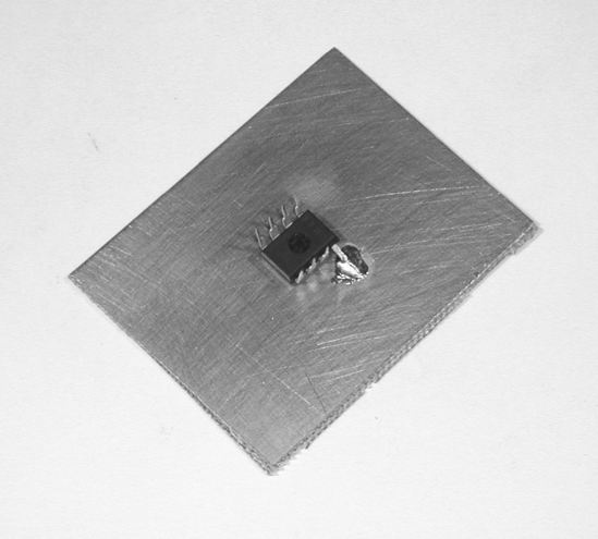
Solder C2 to Pin 5 and to the PC board. Having two pins soldered holds the IC steady.
Tip
When soldering IC pins to the PC board, it works best to make a small bump of solder on the board, tin the IC lead, then place the IC lead on the solder and heat both together.
Warning
Remember that all the IC pins are mirror-imaged when the board is turned over on its back! It may help to make a pencil mark next to Pin 1 on the IC's bottom surface to help you orient yourself as you work.
Bend Pins 4 and 8 of the IC over the body of the IC, and then solder a short piece of bare wire to them, leaving some wire sticking out for contact later. This will be the +12V connection to the circuit.
Solder one pin of the switch to the PC board, close enough to the IC so Pin 2 can be bent out to touch the remaining pin of the switch. Solder Pin 2 of the IC to the switch pin.
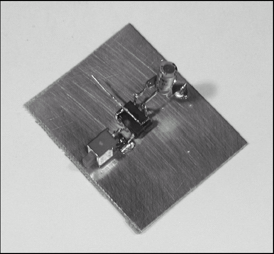
Squeeze Pins 6 and 7 of the IC together and solder them together. Then solder C1 from Pins 6 and 7 to the PC board.
Tip
Keep the bits of bare wire left over from trimmed components. They will come in handy for making short jumper connections.
Tip
If getting a good connection between wires or IC pins is difficult, just tack the component in place with a couple of light connections, and then go back and do a more thorough job of soldering when the component is held steady.
Tip
Leave plenty of room near the IC for connections, since this area gets crowded quickly. Tin the leads of components first for quicker, more solid soldering and sturdier mechanical connections.
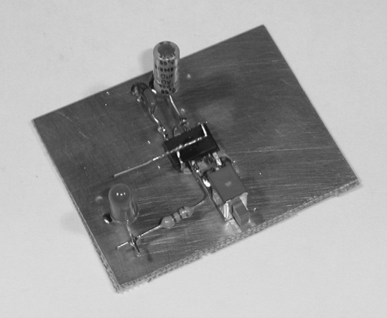
Solder R3 and the anode (for help identifying the LED leads see Step 5 of "Constructing the Digital Timer" in Chapter 3) of LED D1 together, then solder the other lead of R3 to pin 3 of the IC and the cathode lead of the LED to ground. (You can be sure you have the anode and cathode correctly identified by using your multimeter to test the LED in the same way you would test a diode.)
Solder R2 between C1 and the +12V wire connected to IC pins 4 and 8. Solder R1 from S1 to the +12V wire.
Note
The junction of two wires should not be under tension when soldered. A junction that wants to pull apart may spring apart later when another wire is soldered on.
Tip
It's a little easier to make contacts with wires at right angles if the layout permits. Avoid butt contacts with the wire ends coming directly together, as they are very difficult to solder correctly. Overlapped end-to-end connections work fine.
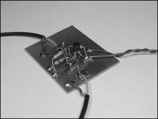
Attach the wires that you intend to connect to the power supply.
Give your circuit a very close inspection, looking for balls of solder, loose wire bits, accidental short circuits, and unsoldered open circuits. Test the circuit by applying power. The first time power is applied, the LED will light until C1 charges to a level that equals 2/3 of the voltage at VCC. When the LED goes out, the circuit is ready to work. Press the switch; the LED should light for about 11 seconds, and then go out again.
Tip
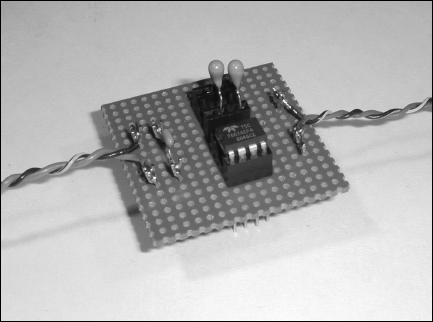
To help manage the rat's nest of wires and leads, twist any pairs of wires that carry power or ground as shown in Step 10's figure.
Note
If your LED doesn't come on and your IC gets hot, you probably wired it backwards. This is a very common error for folks who are just learning the dead-bug technique. Unfortunately, the IC probably didn't survive either, so you'll have to get a new chip and rewire the circuit! If the IC isn't hot, but the LED still doesn't come on, watch Pin 3 with your voltmeter as you press the switch. If it doesn't show a positive voltage, check Pins 6 and 7 to see whether C1 is charging and discharging. Use the circuit's operation descriptions to guide your testing efforts.
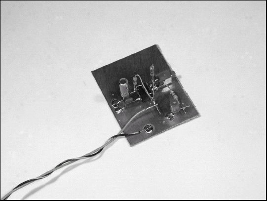
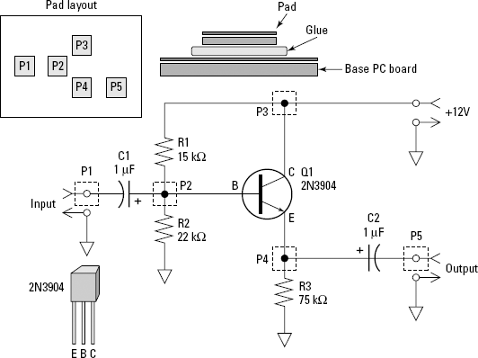
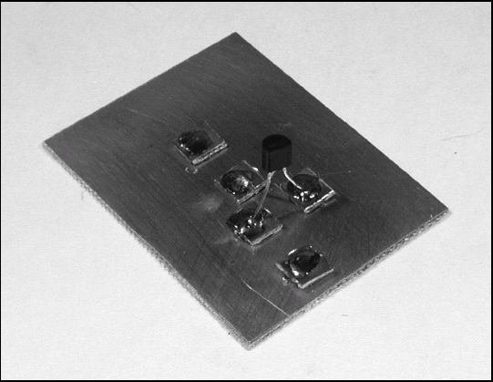
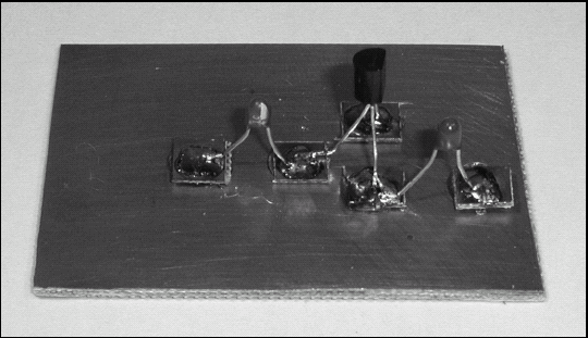
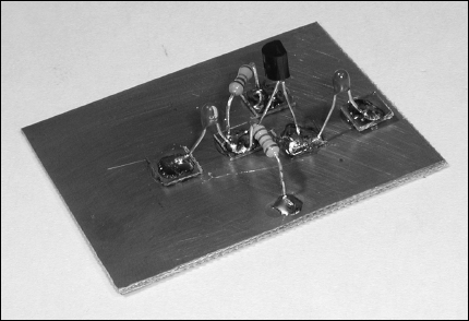
The shortwave signal buffer circuit shown in the following figure will be used to demonstrate Manhattan-style circuit construction. This simple transistor amplifier is used between a short receiving antenna, such as a telescoping whip, and a radio receiver's input. If you've ever used an audio transformer to connect a high-impedance microphone to a low-impedance PA system input, this circuit accomplishes much the same thing. It will buffer (meaning to isolate) signals across the lowerfrequency shortwave bands up to a few megahertz. The output is suited for connection to the customary low-impedance, 50Ω radio inputs.
The circuit has no voltage gain at all, but does increase the output power because it can deliver the same voltage to a much heavier load. (You can find a good overall description of transistor functions and basic amplifiers at www.faqs.org/docs/electric/Semi/SEMI_4.html.) There may be somewhat better transistors to use than the 2N3904, but it is widely available and tolerant of the occasional abuse suffered during experimentation. As this is a demonstration project, the 2N3904 will do the job.
Start by making a photocopy of the schematic and makinsure you have all the parts ready to go.
Cut and clean a rectangle of PC board material about 1 ½" square, as shown in the task "Constructing the Regulator" in Chapter 5. Size is not critical; it's better to have the board be a little too large than too small. You can use either single-sided or double-sided PC board. Cut the board by scoring it with a metal straightedge and sharp utility knife. Score the board on both sides and then bend it over the edge of your workspace or in the small vise.
Tip
Use a fine (small-tipped) pair of needle-nose pliers. The larger needle-nose pliers are more suited to mechanical chores and are too coarse for the job at hand.
Put a small dot of hot glue in the middle of the PC board, quickly attaching one of the pads at the position marked P2 (see Figure 6-4 earlier in this chapter). Repeat for pads P3 and P4 to form a triangle with about ½" between pad centers. The 2N3904 transistor leads will be soldered to these pads. Remove any strings or drips of glue as you go.
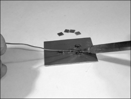
Hot-glue the input and output pads, P1 and P5, to the base PC board.
Tin all pads. Keep the iron on the pad just long enough to melt some solder and make a small pool. Use your multimeter to check for and remove accidental short circuits between the top of the pad and the base PC board.
Tin the leads of the transistor, spread them apart slightly, and flare the ends of the leads so the last ⅛" or so is parallel to the surface of the PCB. Solder them to pads P2, P3, and P4 as shown in the photo.
Solder C1 between pads P1 and P2 and C2 between pads P4 and P5. Be careful to orient them in the correct polarity.
Tip
Have the pad ready in one hand while putting the drop of melted glue on the PC board and place it quickly. The glue will solidify rapidly as the copper coating of the PC board conducts the heat away. Don't worry about getting the pad square with the other pads — that doesn't matter just now, and you'll get a chance to realign the pads slightly in the next step.
Solder R1 between pads P3 and P2 and R2 from pad P2 directly to the PC board as ground.
Solder R3 from pad P4 directly to the PC board as ground.
Tip
The tinning will melt the glue, so don't move the iron around, just press the pad against the board. Use the tip of the iron to align or rotate the pads, if necessary. Don't move them around very much as that will just smear the glue. It doesn't matter if the pads don't all wind up square and neat — the electrons won't care!
Attach the power leads to pad P3 and directly to the PC board as ground. Connect the input and output signals (shown in the figure as miniature coaxial cables) at pads P1 and P5, respectively.
Test the circuit by listening to your radio while turning the circuit's power ON and OFF. You should be able to hear a change in the background noise level, at least. If you can tune in a weaker signal, such as a distant AM broadcast station, the signal should be louder or clearer with the buffer circuit turned ON.
Note
If your buffer makes signals weaker or less clear, you may have the transistor hooked up improperly or one of the capacitors hooked up backwards. Double-check your connections and make sure you have all the resistor values correct. There should be about 0.6-0.7V from the transistor's base to emitter leads. The emitter voltage to ground should be about 0.3V and the collector voltage to ground the same as your power-supply voltage.
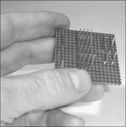
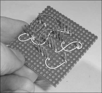
In this task, you'll create a handy little circuit: a DC-to-DC converter that changes a positive voltage to a negative voltage. It's very common to need a small amount of power at a negative voltage, and adding another power supply can be quite expensive. By providing that power with a DC-to-DC converter, the job is done at a lot less expense. This simple circuit is a good way to learn the basics of wire-wrapping. Refer to Figure 6-8 for the schematic.
Start by making a photocopy of the schematic and making sure you have all the parts ready to go. Layout is not critical to this circuit, but a suggestion is shown in Figure 6-8. Placing the input and output connections at opposite sides of the perfboard and the two sockets side by side in the middle helps organize the connections.
Score and break a piece of perfboard about 1 ½" square, using the same technique as for the Chapter 5 task "Constructing the Regulator."
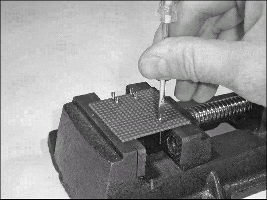
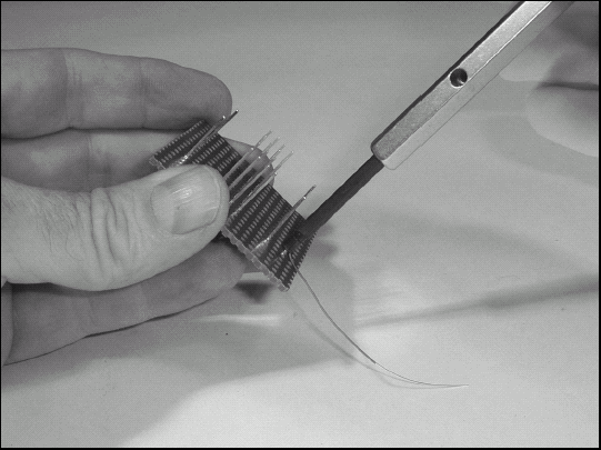
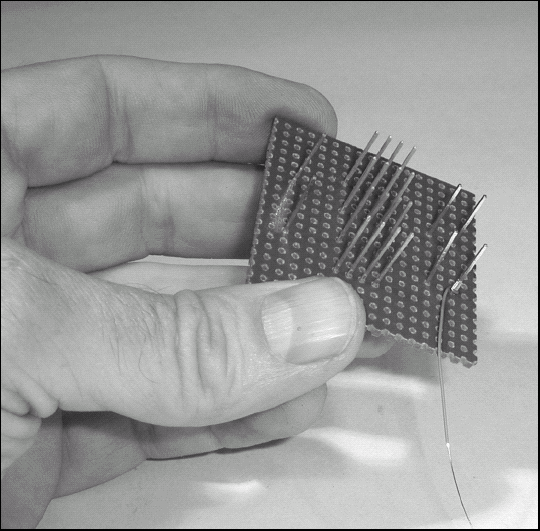
Press the separate pins into the board, using a small screwdriver.
Place one of the sockets on the board, noting which is pin 1. If you have a pin label, use it, otherwise place some tape across the sockets to hold them on the board.
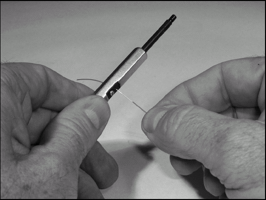
Prepare the first wire by cutting a piece of wire-wrap wire 3" long. Use the stripping tool to strip 3/4-1" of insulation from each end of the wire. This is done by pressing the wire into the narrow slot between the stripping tool's fingers and pulling the wire out. You may need to use needle-nose pliers to grasp the insulation; the wire is quite thin.
Tip
When placing sockets on the board, they should all have pin 1 oriented in the same direction. This makes it easier to keep pins identified. If you have some sockets at right angles to others, keep the orientation of the sockets consistent in each group.
Warning
As with dead-bug construction, the pin layout is mirror-imaged from the Top View.
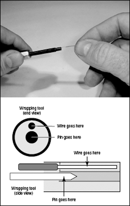
Insert one stripped end of the wire into the end of the wrapping tool, as shown in the figure. The drawing Wrapping tool shows where the wire should go and where the pin will go.
Slide the tool holding the wire down onto the positive-input pin. It should go all the way to the bottom.
Turn the wrapping tool clockwise until the wire is completely wrapped around the pin.
Insert the other end of the wire into the wrapping tool and repeat for the adjacent pin of the bypass capacitor, C3. If you're unsure of your technique, this would be a great time to practice, wrapping several wires until you feel like you've got the hang of it. Then remove them (as described in the sidebar "What Happens If You Change Your Mind?"); the pins won't wear out and can be wrapped over and over again.
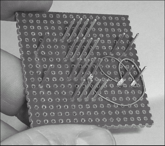
Repeat the process to connect the same pin of C3 to pin 8 of the IC socket.
Tip
Wire-wrap wires are usually cut somewhat longer than the path between pins. This allows plenty of wire to form the initial cushioning wraps and it's usually more convenient than trying for a direct route. The extra length allows you to place the wires between (and away from) the pins as well.
Use another pair of wires to connect the negative input pin to the remaining pin of C3 and to Pin 3 of the IC socket.
Connect Pin 5 of the IC socket to the negative output pin.
Tip
You can see why it's a good thing to have different colors of wire: If everything is just white or black or red, it can be very difficult to trace connections and keep everything straight.
Connect the leads for C1 by connecting pin 2 of the IC socket to pin 2 of the capacitor socket (C1 positive lead). Connect Pin 4 of the IC socket to pin 7 of the capacitor socket (C1 negative lead).
Connect the leads for C2 by connecting Pin 4 of the capacitor socket (C2 negative lead) to the negative output pin. Connect Pin 5 of the capacitor socket (C2 positive lead) to the output ground pin.
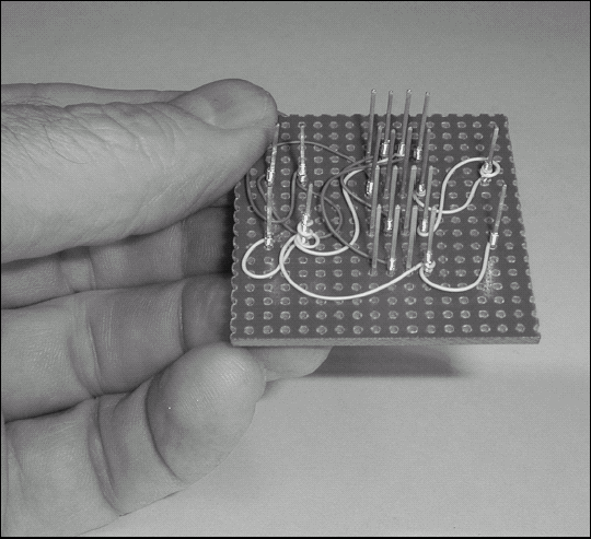
Finish the ground connections by connecting pin 5 of the capacitor socket (C2 positive lead) to the input ground pin.
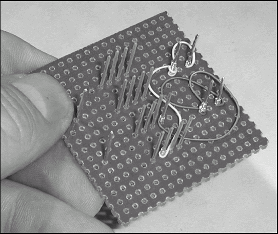
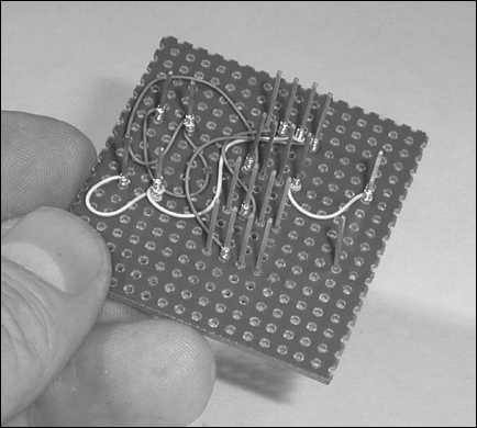
Install the IC and capacitors in their sockets. Use needle-nose pliers to insert the capacitors' leads into the sockets.
Tip
If the circuit has a lot of discrete components, solder them to a DIP header and then insert the header into a wire-wrap socket.
Solder the bypass capacitor, input, and output connections.
Test your circuit by applying power to the input connections and measuring the output with your voltmeter. The output voltage will be slightly less than the input voltage, but with the opposite polarity.
Note
If your voltage converter doesn't work properly, check to make sure the IC and capacitors are inserted correctly into their sockets. It's quite easy to get things reversed between the top and bottom of the board! Also be sure that capacitors C1 and C2 were installed with the correct polarity. If you still have no output, carefully trace your connections and use a magnifying glass to look for accidental short circuits between socket pins.