
Chapter 7
Dielectric Materials under Electron Irradiation in a Scanning Electron Microscope 1
7.1. Introduction
The study of electron irradiation of dielectric materials is of considerable interest from a fundamental point of view as well as from the point of view of applications. Research has covered a wide domain of applied physics, from the behavior of satellites subject to cosmic radiation in space research, to electrets used in radiobiology; we try to avoid the charging up of dielectric materials on board satellites in space and subject to solar winds, while we use charging up of dielectric materials to produce electrets. Dielectric material irradiation by energetic electrons is accompanied by numerous complex phenomena, notably secondary electron emission, photon emission, trapping of charges, luminescence, etc. In the case of conductors, secondary electron emission is a source of issues for particle accelerators, while it is the base of the contrast observed in electron microscopy and exploited in the manufacture of electron multipliers. In the case of irradiated insulators, the situation is different: their secondary electron emission contributes to strange effects, commonly called charging effects, which are irregular and hard to predict.
Although these complex effects are qualitatively well understood and have been described in a proliferation of articles (the complete list of which is impossible to detail here but which is previewed in this special issue [JES 92]), the physical mechanisms of the elementary physical phenomena brought into play are far from being explained.
This chapter deals with the different aspects of charge effects of insulators under a low energy electron beam (between 300 eV and 30 keV) in a scanning electron microscope (SEM) with, in particular, the analysis of parameters implied, notably the sample, its geometry and its environment (i.e. a vacuum) as well as the irradiation conditions (energy, intensity, beam size, etc.). Before tackling the charge phenomena resulting from the electron bombardment of an insulating material, we shall first inspect the basic elements associated with the electron-matter interaction in general and electron-insulator in particular. The different physical processes which accompany the injection of a charge into an insulator and the behavior of this latter following injection will be described. The general properties of insulators, such as the role of disorder in charge localization, the influence of defects, either intrinsic or induced by electron irradiation, and the processes of charge transport will also be presented. The influence of charging phenomena on emitted signals, notably electron emission andemission of X-rays, will then be tackled. The amplitude of these phenomena is often difficult to predict, because they are not only a function of the chemical composition of the sample but also of unknown structural parameters, such as the density of traps as well as the often complex conduction surface mechanisms. They will then be studied by developing some recent experimental techniques and illustrated by numerous examples.
7.2. Fundamental aspects of electron irradiation of solids
7.2.1. Volume of interaction and penetration depth
During the progress of an electron of energy E0 in a solid sample, we usually distinguish two types of concomitant interactions: elastic and inelastic interactions [SEI 84]. The interaction is elastic when an electron penetrating the influence zone of the potential which reigns around an ionic core is deviated without any appreciable energy loss. If the energy of the electron varies in a significant way, for example by transmitting part of its energy to an atomic layer electron, the interaction is said to be inelastic. According to these two types of interactions, incident electrons take random routes in a material until total loss of their kinetic energy. An example of these trajectories obtained by numerical simulations, according to the Monte Carlo method, is given in Figure 7.1(a); the place where all of these interactions occurs is called the “volume of interaction”. The lateral dimensions zm (average penetration depth, from a few nm to a few μm) of this volume depend mainly on the incident energy and the physico-chemical properties of the target [FIT 74].
7.2.2. The different emissions
In the volume of interaction, multiple emissions with different physical natures are generated. Mainly, these are the electron emission, photon emission, cathodoluminescence, plasmons (due to collective oscillations of valence electrons), phonons (associated with the thermal agitation of a periodic structure), as well as the creation of electron-hole pairs. Most of these signals, illustrated in Figure 7.1(b) in the case of a thin target, are produced simultaneously and make possible the observation and analysis of a chosen object in a scanning electron microscope.
Figure 7.1. (a) Electron trajectories simulated by the Monte Carlo method in a grounded gold coated Al2O3 at 20 keV [JBA 96b]. (b) Electron bombardment of a thin target and resulting signals

For simplification, and for the needs of this chapter, electron emission (i.e. secondary and backscattered electrons) and photon emission (X-ray photons) are described very basically below.
7.2.2.1. Electron emission
7.2.2.1.1. Backscattered electrons
These electrons from the primary beam come out of the irradiated material after having given up (or not) a more or less large part of their energy. They come from an average depth estimated at R/2 (R maximal penetration depth) by Niedrig et al. [NIE 82], and their spectral distribution coming out of the target ranges from 50 eV to the energy of primary electrons. We often characterize backscattered electrons by what we call the backscattering coefficient η defined by the ratio of the current intensity due to the backscattered electrons, Ir, to the primary current intensity I0. For literature concerning the importance of backscattering, see [NIE 82] (and included references); here we content ourselves with a brief reminder of some characteristic notions of this emission [JOY 95]:
– for a primary energy ranging between 10-30 kV, the backscattering coefficient is practically independent of the primary energy;
– for low energies, the coefficient decreases as a function of energy for targets composed of light elements and increases for targets composed of heavy elements.
7.2.2.1.2. Secondary electron emission
The phenomenon of secondary electron emission was subjected to numerous theoretical as well as experimental research concerning the mechanisms and elementary processes which play a part in this emission. At the present time, the most complete and satisfying interpretation on the emissive properties of metal targets can be found in the articles of Dionne [DIO 75], Schwarz [SCH 90] and Shih [SHI 97].
Mechanism
The secondary emission phenomenon occurs according to three different processes: generation, transport towards the surface of the sample and, finally, the crossing of this latter. The generation of secondary electrons takes place along the course of primary electrons in the volume of interaction and happens isotropically. By losing part of its energy, the incident electron excites the electrons in the external layers of the atoms in the target which are weakly bonded. The depth distribution of the secondary electron production rate is proportional to that of the energy losses. The emission being isotropic, only a fraction (to a first approximation, half) of the electrons generated migrate in the direction of the target/vacuum interface. However, because of the interactions with the electrons of the conduction band and with the phonons, only the electrons created between the surface and what we call the escape depth reach this interface. According to the works of Seiler [SEI 67] the maximum escape depth of secondary electrons is about 5λ (λ being the mean free path of the secondary electrons). Let us note that the transport of secondary electrons towards the target/vacuum interface is weaker in an insulator than in a metal because λ ≈ 0.5–1.5 nm in metals, while in insulators λ ≈ 10–20 nm [SEI 67]: secondary electrons interact exclusively with phonons. Further, to cross the target/vacuum interface, the secondary electrons must have at least an energy equal to the work function in the case of a metal or to the electron affinity (minimum energy required to be supplied to an electron situated at the bottom of the conduction band to eject it in a vacuum) in the case of an insulator or a semiconductor. As an example, the electron affinities χof alumina (Al2O3) and silicium (SiO2), both monocrystalline, are close to χ = 1 eV [ALI 78]. The emitted secondary electrons are not very energetic (between 0 and 50 eV, according to conventional limit) and come from regions near the surface (of the order of a few nm). The secondary electron emission rate or secondary electron yield, δ, is defined as being the ratio of the intensity of the secondary electrons current to that of the primary current.
Total emission yield
The total electron emission yield σ is defined by the following relation:
where δ is the secondary emission yield and η the backscattering coefficient.
Figure 7.2 schematically represents the characteristic shape of this yield and its two components δ and η as a function of the energy E0 of the primary beam.
Figure 7.2. Schematic layout of total electron emission yield aas a function of primary electron energy

The shape of this curve is the same for all materials. With the backscattering coefficient η being practically constant and its variation very weak (compared with δ), the shape of σ is consequently dictated by the yield variation δ, except at very low energies. To explain the total electron yield variation σ as a function of the primary energy E0 and the influence of the incidence angle on the secondary emission yield, see [SCH 90] and [JOY 95].
7.2.2.2. Emission of X-ray photons
We have seen that when electrons make their way in a material medium, they interact with it, undergoing elastic and inelastic collisions. These latter inelastic collisions can give rise to vacancies in the internal layers of the atoms which are thus found in an excited state. The return to an equilibrium state (de-excitation) occurs either by radiative emission (X-ray emission) or by non-radiative emission (Auger emission). In the first case, the created vacancy is filled by an electron from an upper layer (the transition obeys the selection rules of quantum mechanics) and the energy difference between the two levels brought into play is transformed into an X-ray photon (Figure 7.3).
Figure 7.3. Schematic illustration (Bohr model) of the emission process of (a) characteristic X-ray photons or of (b) Auger electrons emissions
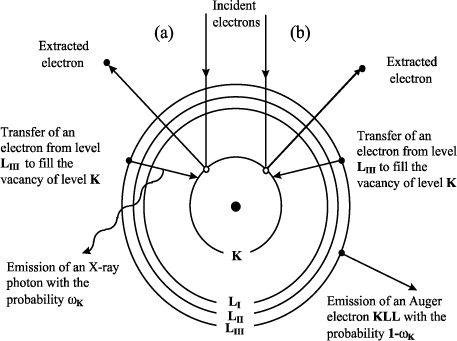
The electron irradiation of a material is then accompanied by the emission of X-ray photons with the well-defined energies and characteristics of the atoms composing the target. This mechanism constitutes the basic principle of X-ray microanalysis. Besides this characteristic emission, the electron bombardment of a solid target generates a continuous radiation related to the slowing down of incident electrons in the strong electromagnetic fields of the atom cores in the target. In X-ray microanalysis, this radiation (Bremsstrahlung) constitutes the continuous background on which the characteristic lines will appear. Please note that the maximum energy of this continuous X-ray radiation, which could not exceed the energy of the primary electrons, represents a limit which we call the “Duane–Hunt limit” and which we often use to control the acceleration tension of the scanning electron microscope on metallic targets, or to measure the surface potential when we deal with insulating targets (see section 7.4).
7.3. Physics of insulators
7.3.1. General points
Materials known as insulators, which we come across everywhere in our environment (glasses, ceramics, metal oxides, micas, rubber, paraffin, paper, polymers, composites, etc.) have resistivities much greater than those of metals and semi-conductors, even intrinsic resistivitities with a large band gap (see Figure 7.4). As was shown in Chapter 2, (section 2.1 and Table 2.1), this is mainly due to a very weak density of mobile charge carriers, although the mobility of these carriers can often approach that of metals, or even exceed it. Insulators have a very weak conductivity because of the absence of free charges and not because they are unable to conduct these charges. Another property is that, unlike metals, insulators trap charges because of the defects and the impurities they contain. This leads to the “charge phenomena” described in Chapter 2. Insulators can also get polarized when an electric field is applied to them.
Figure 7.4. Range of electric conductivities of insulators compared with those of metals and semi-conductors (in Ω−1.cm−1)

7.3.2. Insulators under electron irradiation
7.3.2.1. Microscopic phenomena
7.3.2.1.1. Secondary electron emission of insulators
During the electron irradiation of an insulator, electron-hole (e.h.) pairs are created along the path of the incident electron, until its maximal penetration depth R.
This creation essentially results in two processes, one is direct (Valence Band (VB)-Conduction Band (CB) transition) and the other is indirect (relaxation of plasmons). The number of e.h. pairs created by the incident electron is n(e.h.)=E0/E(e.h.) (with E0 energy of incident electrons, and E(e.h.) creation energy of a pair which ranges between 10 and 25 eV in the materials being considered) [CAZ 99 and some references included]. The very slow electrons (a few eV from the bottom of the CB) resulting in the creation of these pairs and which do not spontaneously recombine with the holes, propagate in the insulator and can escape in vacuum if their final energy is greater than the affinity of the insulator. Withing the framework of this study, it is interesting to compare the secondary emission of metals with those of insulators under electron bombardment, knowing that this comparison is difficult because, as the insulators get charged, the yield varies. This comparison is illustrated in Figure 7.5a.
The emission peak of metals has a width larger than that of insulators. It is of the order of 10 eV for metals and 5 eV for insulating materials [WHE 64]. The weakness of electron density in the conduction band leads to a maximal secondary emission δm which, for uncharged insulators, can be of an order greater than that of metals. The maximal secondary emission of metals generally ranges between 1 and 2; that of insulators is a bit more than one order of magnitude greater; that of polymers is often limited to the interval 3 < δm< 7 [WIL 73]; for monocrystalline MgO, δm ≈ 22 [WHE 64] and this yield can reach extremely high values such as recently obtained with a diamond sample (δm ≈ 84) [SHI 97] at an energy of 3 keV.
The differences observed in the secondary emission of the two classes of materials can be discussed in a qualitative manner from the study of secondary electron generation and their transport until exit at the surface of the samples. Several theoretical discussions [SHI 97, KHA 82, AKK 94] attribute the observed experimental results to the lack of electron-electron interaction during the transport of secondary electrons generated in insulators, and to their very low or equally negative affinity. This lack of electrons allows an increase in the mean free path (in uncharged insulators) and a weak affinity often allows the generated secondary electrons to escape in a vacuum [SHI 97]. The escape depth (the mean depth in the insulator from which the electrons are emitted, which governs the value of δ) of the secondary electrons (λ ≅ 50–100 nm) is greater than that of metals (λ ≈ 5–10 nm). The interactions of secondary electrons with phonons or with crystalline defects explain the reduction of this depth when the temperature increases (see Figure 7.5b) or when a polycrystalline sample (rather than a monocrystalline sample) is irradiated [CAZ 93]. For irradiated insulators, the secondary emission in a vacuum in principle leaves a positively charged zone at the surface of the sample, and the resulting charging effects lead to self-regulation processes which limit the secondary emission (see section 7.3.2.2.2).
Figure 7.5. (a) Comparison of secondary emission yields of insulators and metals. (b) Escape depth λ of secondary electrons as a function of their kinetic energy [CAZ 95a]

7.3.2.1.2. Induced defects and desorption of species
The interaction of incident particles with target electrons and atomic cores leads to the creation of defects which are generally classified in two categories: those which come from the bond breakdown due to ionization of the atomic levels and those which come from lattice distortion due to an atomic displacement. The latter is unlikely in SEM irradiation conditions because it occurs when the high energy incident particles interact with the lattice.
The bond breakdown is due to the atomic level ionization of the target components by the incident electrons which leads, by de-excitation, to the emission of X-ray photons with probability ωij and the emission of Auger electrons with complementary probability aijk. Following the electron vacancy created (in just a few 10−15 seconds), cascade transitions, implying more and more external electron levels, are generated. The final electron levels thus become depleted of electrons. In the case of metals, the electronic charge of each atom is restored by conduction electrons, whereas in the case of insulators restoration is not possible since these electrons are virtually nonexistent.
Thus, in irradiated oxides the ionization of oxygen at the 1s level will (temporarily) transform the 02− ion into 0° (by the most probable emission, aijk > 99%, of the Auger electron OKLL) while in irradiated fluoride, the ionization of the 1s level of fluorine will transform the F− ion into F+ (probably due to the emission of the Auger electron FKLL). There can be electron rearrangements with neighboring atoms but inversion of the polarity of certain “halogeneous” ions will lead to the inversion of their Madelung energy and their (coulombian) expulsion from their initial site [SAT 91], [CAZ 95b], [JBA 96b]. The most spectacular result then concerns the possibility of atom displacements (and their desorption in vacuum) of atom species (initially negative) by simple irradiation of insulators with the aid of incident particles (electrons or X-ray photons) whose initial kinetic energy cannot exceed 1 keV [BEN 97].
Silicium, alumina [JON 00] and quartz [VIG 85] are three examples of materials whose defects induced by irradiation are fairly well described in the literature. These defects are often identified with the aid of techniques such as electron paramagnetic resonance (EPR) and the mechanisms proposed for their interpretation are different to those based on the Auger mechanism discussed above.
In the case of silicium, the defects are essentially of three types: the first is oxygen vacancy (neutral, denoted as ≡ si−…−Si ≡, or positive, called the E′ center, and denoted as ≡ si−…−Si ≡) accompanied by a relaxation of neighboring atoms. This type of process is favored if the hole is generated in the part of the valence band corresponding to the Si-O bonds [WEE 56], [GRI 80], [FEI 74], [EDW 82]. The second type is radical peroxide (≡ Si - O - O−), which can result from either an E′ center or a peroxide bridge (≡Si-O-O-Si ≡) [STA 78], [GRIS 81]. The third type is a non-bonding oxygen or silicium (NBO) [STA 79]. These defects are associated with bond breakdowns in the sequence between silicium and oxygen atoms, characteristic of a local disorder. These breakdowns can be created by irradiation or during the elaboration of silicium. In the case of quartz, the induced defects are essentially crystalline lattice defects induced by irradiation which favor the formation of excitons responsible for the creation of oxygen-bond peroxide vacancy pairs [VIG 85].
In the case of alumina, in the fundamental state, the electron configuration of oxygen is near O−. At an oxygen vacancy position, we would expect an equivalent electron distribution of about one electron. Owing to the absence of the atomic core, this distribution is strongly coupled with the vibration modes of the lattice. Such a center is called an F+ center. An electron state localized in the band gap, partially occupied by electrons from the lattice, is associated to an F+ center. The trapping of an electron by an F+ center gives an F center (oxygen vacancy occupied by two electrons). The occupied electron state associated to the F center is less strongly bonded than that associated to the F+ center. With each F+ and F center are associated excited levels. The trapping of an electron is exclusively made through weakly bonded levels, and therefore situated very near the bottom of the conduction band. For an F+ center, it is made in strongly excited states.
Based on an interpretation of the Auger mechanism, as well as the trapping phenomenon (see section below), one of the consequences of the desorption initiated by this mechanism is the fact that the O2− ion of the oxides becomes neutral, leading to a reduction of associated metals (or semi-conductors). The desorption can get amplified when the excited atoms belong to the third line of the periodic table, from Na to Cl, because the Auger mechanism can lead to the loss of 4 electrons (KLL transition followed by two LVV transitions). Other mechanisms can be implied in the creation of defects, the production of charged ions in partially ionic solids. These effects, which allow explanation of the electrical migration of negative species and their ejection in vacuum for electron irradiated insulators by electrons, have been subjected to numerous works in the literature [JBA 95], [GED 99].
7.3.2.1.3. Trapping and charge transport
The different processes
Several approaches have been proposed to interpret the phenomena of conduction and trapping of electrons in an insulator. The first approach originates in the high resistivity of the insulator to electric current, which amounts to saying that the charges are fixed by an ohmic process. The injected charges could slowly flow, and, after thermalization, appear virtually motionless. The constant τ = ε.ρthen represents the characteristic time of this type of propagation, obeying an exponential law e−t/τ. The time constant values τ of most insulators are of the order of 10−7s to several days. This approach, however, comes up against two problems: the first is due to the fact that there are insulators, notably monocrystalline ceramics such as MgO, Al2O3 (sapphire), which may not get charged at room temperature after an appropriate thermal process. The second concerns the fact that the resistivity cannot show the ability of the insulator to trap electrons through an ohmic process. Indeed, the notion of resistivity is applied to intrinsic charge carriers of the material, while the charge phenomena are due to external charge carriers injected into the solid.
Another approach is based on the band structure by assuming the existence of localized energy levels in the band gap due to defects (impurities, dopants, etc.) and electron states localized at the bottom of the bands (CB or VB) (Anderson states) (see Chapter 2, section 2.3.2). This latter seems incomplete because it neither takes into account the polarization effects of the material around a trapped charge, nor the thermodynamic property changes brought to the fore by Moya [MOY 93]. Finally, the approach which gives a more global explanation of the trapping process is that made from the polaron theory described in Chapter 2.
After this description of different trapping approaches, we can say that, once it penetrates a bombarded sample, an electron loses its kinetic energy, either by giving it up to the lattice, or by exciting electrons from the medium. Electron-hole pairs are created in the insulator but the majority of these pairs quickly recombine and only a few electrons and holes move in the conduction and valence bands before getting trapped (again) at the localized levels of the band gap, representing the impurities and the structure defects produced under electron irradiation and/or pre-existing in the material. The ability of electrons to get trapped is an increasing function of the density of the trapping centers and their trapping energy [CAZ 96 and references included]. This ability then increases with crystalline disorder, i.e. by passing from the monocrystalline state to the amorphous one. The distribution of different trapping centers characterized by their trapping energy, well known for silicium, can partly be revealed by cathodoluminescence experiments, underscoring the relation between trapped charges and color centers [JAR 95]. In the ideal case of a perfectly monocrystalline insulator without structural defects (neither pre-existing, nor induced by incident radiation) and without impurities, the trapping of electrons can only be conceived on the surface of the sample [CAZ 90], [CAZ 91], [REM 98]. If the ideal insulator is earthed, the injected excess electron will quickly be evacuated and no charge localization (or trapping) is possible.
Mobility of charge carriers in disordered insulators
The effects of disorder on the localization and transport of electrons injected in an insulator was recently reviewed by Blaise [BLA 01] and described in Chapter 2. Although this analysis does not include effects due to the electric field induced by a trapped charge itself on electron transport, that is to say the detrapping of trapped charges and the slowing down or acceleration of charge carriers [CAZ 99], [WIN 97], [PEP 98], we can say that, according to the degree of disorder, there is a competition between the conductivity due to mobility in extended states and the conductivity due to mobility in localized states (at the bottom of the conduction band). It should be noted that, for a certain number of insulators and from a certain degree of disorder, the conduction in localized states is activated at room temperature.
7.3.2.2. Macroscopic phenomena: charging effects
The only common characteristic of the diverse varieties of insulators under electron irradiation is that their weak electron density in the conduction band forbids them from spontaneously compensating the electric charge deficiency which results from this irradiation. As a result of this, two types of phenomena inherent to the electric field created by the excess electric charge (+ or −) are addressed below: on the one hand, the effects of direct charges which lead in particular to the deflection of the incident beam (responsible for the distortion of the electron image in an SEM) and the modification of the physical parameters of electron-matter interactions which leads notably to the modification of the secondary emission and the X-ray emission, and on the other hand the possible chemical modification of the sample which results from the migration of mobile ions or the stimulated desorption of species. The literature abounds with descriptions of charge phenomena and it is impossible here to draw up an exhaustive list; readers are directed to a few notable articles which deal with these phenomena: [VID 95], [CAZ 99b] and [VID 01].
7.3.2.2.1. General law of conservation of current and induced charge
The total accumulated charge in an insulator results from the competition between electron emission, trapping and charge transport.
If I0 and IL are, respectively, the primary current and the leakage current resulting from the transport of a few electrons towards the ground, the law of conservation of current is then written as:
where σ is the total electron emission coefficient and dQ/dt the trapping rate during the charging process.
Conceptually, the total charge, Q, can be positive or negative depending on whether the secondary emission prevails or not over the incident electrons implanted and evacuated. If Q is > 0, the current IL will be ohmic (due to conductivity) whereas when Q is < 0, this current is non-ohmic (related to I0).
The positive charge which results from the secondary electron emission, δ, extends on a layer of thickness corresponding to the emission depth of the secondary electrons. The negative charge resulting from the injection in the sample of incident electrons (less the backscattered electrons) extends on a layer of thickness R approximately corresponding to the maximal penetration depth of the primary electrons. The global charge of the sample will then depend on the initial primary energy value, E0.
7.3.2.2.2. Self-regulation and conventional approach: sign of the induced charge
During electron irradiation we see a competition between the positive charges resulting from the secondary emission and the negative charges resulting from the trapping of incident charges in the insulator. In the absence of leakage current, the compensation phenomena take place and lead to a final state characterized by a total unitary yield which corresponds to the identity between the current entering and the current exiting the sample. If the initial state of the sample is characterized by δ+η>1, the positive excess charges lead to a positive surface potential VS which reattracts the slowest secondary electrons and freezes their emission (once Vs reaches a few volts). Conversely, if the initial state is characterized by δ+η<1, the excess negative charges lead to a surface potential which slows down the incident electrons outside the sample; their effective energy at the surface (landing energy) is then E0+qVs (with Vs < 0 and q =1.6.10−19 C) and the secondary emission increases towards a stationary state for which its yield is equal to one. Self-regulation phenomena (freeze or increase of the secondary emission) lead to the conventional approach δ = f(E0) based on arguments taken from the total electron emission yield curve, generally obtained by irradiating the target with short electron pulses, the “pulse mode technique” [ BRU 54], which allows nearly all charging phenomena to be avoided. This approach predicts the sign of most charges implanted in insulators irradiated with electrons. Indeed, the sample gets positively charged when ECI<E0<ECII and negatively charged when E0>ECII (or <ECI). ECI and ECII are the critical energies for which δ+η =1. For most insulators, the use of the impulsion method leads to a total electron emission yield without trapping, often several orders of magnitude greater than that of metals and, consequently, to a critical energy EC2 greater than or equal to 10 keV [WHE 64, SHI 97, CAZ 01].
In the case of permanent irradiation, a negative charge is often observed for primary energies as weak as ECII ∼ 2–3 keV, corresponding to electron emission yield obtained by the pulse method, almost at their maximum [CAZ 01 and included references]; the conventional approach predicts a positive charge in this case. Thus, the predictions of the conventional approach are in contradiction with numerous experimental results [CAZ 01 and included references] notably those about monocrystalline alkaline halogens studied with the impulsion method and for which the maximum of the secondary electron emission yield 8m is systematically greater than 5 (most often 10) for primary energies in the interval 1–2 keV. In the case of permanent irradiation of LiF and NaCl, under normal circumstances, the obtained critical energies ECII are, respectively, 2 keV and 2.5 keV [REI 92], which correspond to a negative charge.
Figure 7.6. Displacement from the critical energy E0CII to the energy E(R = s) under permanent irradiation. The point S being the new equilibrium state (from [CAZ 01]). In the dotted line: schematic curve δ = f(E) of the charged insulator

To discard this ambiguity, an approach recently proposed by our laboratory [CAZ 99], [CAZ 01] permits the nominal yield δ0 (corresponding to the critical energy E0CII) obtained with the aid of the pulse method of the practical yield δ (corresponding to the critical energy ECII) obtained using a permanent irradiation to be distinguished. In the case of permanent irradiation, laboratory analysis suggests that a surface potential equal to zero can only be reached when the penetration depth of the primary electrons is close to the escape depth of the secondary electrons. This state corresponds to the new critical energy ECII=E(R=3s) (Figure 7.6), slightly higher than the energy corresponding to the maximum of the function δ, and therefore less than E0CII.
In conclusion, the conventional approach of the total electron emission yield can be applied in conditions of use of a permanent irradiation only by replacing the critical energy E0CII with E(R ≈ 3s). The consideration of current leakage leads to a partial evacuation of the excess negative charge, and consequently a reduction of the negative surface potential. In this case, the effective energy of the primary electrons can be greater than E(R ≈ 3s) [CAZ 01].
7.3.2.2.3. Deflection of the primary beam
The electric field created within an irradiated insulator is a direct consequence of the trapped charge in that insulator. The deflection of the primary beam (schematically represented in Figure 7.10a) which results from it can be either partial or total. In the first case, it is responsible for the distortion of the electron image and the pseudo mirror contrast [BEL 00b] and, in the second case, it leads to the mirror effect. Although these two effects present disadvantages at both observation and analysis levels (section 7.4.2.2), they carry quantitative and qualitative information on the charging state of the insulator.
Partial deflection
The formation of images in scanning electron microscopy results from synchronous scanning of the sample and the visualization screen whose Wehnelt is modulated by the signal emitted by the different points of the sample under electron irradiation. Each point on the screen (G.x0, G.y0) corresponds to a point on the target (x0, y0), with G being the proportionality factor which defines the magnification of the image (see Figure 7.7a).
However, because of the presence of a “perturbing” electric field ![]() in the vacuum of the specimen chamber, the primary beam initially aiming at coordinates (x0, y0) will be deviated. The primary electrons will then hit the surface sample at a distinct point (x, y). As the scanning of the visualization screen remains synchronous with that of the deflective coils, the intensity affected to the pixel (G.x0, G.y0) on the visualization screen will then be associated with point (x, y), not point (x0, y0). The effect of this desynchronization is an apparent distortion of the scanned zone of the sample (see Figure 7.7(b)). From this distortion, it is possible to determine the quantity of trapped charges and its evolution over time, as well as the corresponding surface potential VS (section 7.4.2.2.1).
in the vacuum of the specimen chamber, the primary beam initially aiming at coordinates (x0, y0) will be deviated. The primary electrons will then hit the surface sample at a distinct point (x, y). As the scanning of the visualization screen remains synchronous with that of the deflective coils, the intensity affected to the pixel (G.x0, G.y0) on the visualization screen will then be associated with point (x, y), not point (x0, y0). The effect of this desynchronization is an apparent distortion of the scanned zone of the sample (see Figure 7.7(b)). From this distortion, it is possible to determine the quantity of trapped charges and its evolution over time, as well as the corresponding surface potential VS (section 7.4.2.2.1).
Figure 7.7. (a) Principle of formation of the image in a scanning electron microscope. (1) Trajectory of primary electrons in the absence of perturbing electric field. (2) Trajectory of primary electrons in the presence of perturbing electric field E. (b) Dynamic distortion of the electron image of a sphere-grid system (left, at t = 0s; right, at t = 70s) (from [BEL 01b])

Total deflection: mirror effect
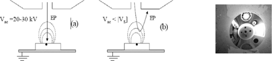
In the extreme case of total deflection of the primary beam, we observe a spectacular effect called the mirror effect. This deflection is produced when the primary energy of the incident electrons is less than the surface potential resulting from the trapped charge in the irradiated insulator. This latter then behaves like an electrostatic mirror and, instead of observing the surface sample, we see the specimen chamber of the microscope (see Figure 7.8 and section 7.4.1).
7.3.2.2.4. Chemical modifications and other irradiation effects
One of the possible consequences of charging effects is the chemical modification of the sample. Besides the external consequences (deflection of the beam), these effects are translated into the establishment of an internal electric field which can be sufficiently large to result in a dielectric breakdown, but they can also induce the chemical modifications of the surface via the migration of mobile ions under the influence of the field. This is particularly the case in the analysis of glass where the concentration of sodium evolves during irradiation [JBA 95], [GED 99]. The electron stimulated desorptions (ESD) of species naturally lead to a chemical modification of the irradiated surface. Amorphous silicium for example can transform into silicium under irradiation [JAR 88] because the ion O2− becomes neutral, leading to a reduction of the silicium. This mechanism could explain the cold recrystallization of amorphous silicium [SAT 91], [CAZ 95b]. This reduction remains valid for metals when dealing with the irradiation of, notably, LiF alkali halides [JBA 96]. Superficial morphological transformations can also be produced when the carbon of organic materials has some electronic bonds with its neighbors which are suddenly cut off.
Figure 7.8. Principle of the mirror method: (a) injection stage of the charge; (b) measurement stage of the charge (obtaining of the mirror image) Vac < Vs (from [BEL 01b]); (c) mirror image from [JBA 04]
It is interesting to mention the fact that charging effects and the phenomenon of species desorption often coexist, as illustrated by the results obtained for SiO2 by Jardin [JAR 88]. Both phenomena can equally interact with one another. Indeed, the electron irradiation (at 1 keV) of KCl leads to the formation of an insulated metallic layer which results from the ejection of chlorine and which thus favors the formation of a negative surface charge [SZY 92].
7.3.2.3. Parameters governing the charge phenomena
The charging effects in close relation to the ability of an insulator to charge are the result of several dynamic physics processes, complex and closely related, depending on numerous “parameters” not only related to the structure and the nature of the insulator, but also to its environment and the irradiation conditions. The organogram below [BEL 01b] shows a list of some of the most relevant parameters when an insulator is in an environment such as that of a scanning electron microscope.
Among the experimental and environmental parameters studied and likely to affect the ability of the insulator to charge, some of them, like the primary current density and scanning frequency, can easily be controllable and fixed. The effects of the parasite source (electrons coming from polar pieces which result from the acceleration and focus of the secondary electrons emitted by the insulator [BEL 00a]) are hardly controlable but can be reduced by covering the polar pieces with light materials. It should also be noted that a sample which has been irradiated can conserve its negative trapped charge for a long time (from several days to several months) even after an input of air into the chamber of the SEM. The neutralization of this charge before a new irradiation can be ensured either by heating the sample (if this sample permits it), or by irradiation with the aid of an auxiliary electron gun of energy E0 such that ECI < E0 < E(R = 3s) (see section 7.3.2.2.2) bringing positive charges, or with the aid of the primary beam whose energy would have decreased [MOR 76], (in this latter case, the sample is not discharged in volume).

On the other hand, contamination remains a major issue whose consequences are important and unpredictable. To completely eliminate this latter parameter, the use of equipment under ultra-high vacuum (i.e. Auger equipment) presents an advantage compared with the use of a SEM; however, decontamination plasma devices especially designed for SEM are being developed. Indeed, apart from the quality of the vacuum, it is possible to check the absence or not of the contamination in real time by means of the Auger spectrum of the irradiated zone. When a contamination is observable, it is possible to eliminate it by steaming and/or ion erosion. In these conditions, it will then be possible to more easily study the relation between the nature of the insulator and its electrical behavior. This relation is conditioned by the regulation mechanisms which are constituted by the secondary electron emission and the charge transport phenomena. These two mechanisms, which are interdependent because of the electric field generated by the trapped charge, must be dissociated. The simultaneous measurement of the influence current and the leakage current allows not only the evolution of the trapped charge during irradiation to be obtained, but also that of the electron emission yield (see next section). The study of the physical parameter effects of the insulator (defects, structure, dimensions, etc.) on electron emission and charge transport can then be undertaken independently.
7.4. Applications: measurement of the trapped charge or the surface potential
7.4.1. Introduction
The electron irradiation within an SEM constitutes a privileged tool for injecting an electric charge into an insulator because it permits on the one hand the circumvention of the disadvantages related to the use of an electrode on the contact of the surface sample (the influence of the nature of the electrode and the additional defects induced at the insulator/metal interface) and, on the other hand, the good spatial resolution of an SEM allows the electron beam to be focused on a small zone and consequently the phenomena which develop in this zone to be explored. Further, on-board experiments to understand the origin of the problems of charging and discharging suffered by the dielectric materials which cover satellites (as a result of their irradiation in space) remain expensive and rare in practice, and electron irradiation in an SEM remains an interesting alternative to best reproduce the space environment in a laboratory.
The reproduction in an SEM chamber of the environment, dimensions and conditions to which an insulator will be constrained in its application medium, also permits us to see which intrinsic parameters of the insulator (composition, structure, dimensions) we must act on during its development so that it can adjust to a desired application.
Diverse methods allowing the evaluation of the ability of an insulator to charge have been developed and implemented within an SEM. They are based on the measurement of the trapped charge in the insulator and its evolution during irradiation. A considerable amount of work has been undertaken to extract information from these measurements concerning the structural, chemical and electrical characteristics of insulators [BRU 83], [VAL 99], [ONG 98], [SON 96], [BEL 00a], [BIG 97], as well as the mechanisms of associated trapping and detrapping.
In this study, we shall not only describe methods using an electron beam or the signals they generate. These methods allow the measurement of the trapped charge (or the resulting surface potential) and its evolution over time. One of these techniques is based on surface potential measurement at the equilibrium state, either by X-ray spectroscopy, or by electron spectroscopy [BEL 01a], [JBA 01]. The second uses the mirror effect. The third is based on the measurement of the dynamic distortion of electron images induced bytrapped charges under electron irradiation [BEL 00a]. The last, which allows the measurement of trapped charge evolution, not only during irradiation but also after irradiation stops, is based on the measurement of the influence current.
Techniques allowing access to the spatial distribution of internal charges in an insulator, notably the thermal and accoustic methods (described by [LAU 99] and references included) are not studied here. Although it is not impossible to adjust them to the chamber of an SEM, these methods, however, present the disadvantage of metallization of the sample surface (electrode measurement). For a more rigorous approach notably to the charging conditions of the dielectric covering of spatial instruments in orbit, it would be useful to develop a measurement system without contact (an idea which worries some laboratories of SEEDS (Système d’Energie Electrique dans leur Dimension Sociétale) dielectrics).
7.4.2. Static methods
These methods are described as static because the measurement time is relatively long compared with the time constants of the observed phenomena. Nevertheless, in certain cases they can be considered as dynamic.
7.4.2.1. Mirror method
The method which uses the mirror effect, the “mirror method” [LEG 91], [VAL 95], [VAL 99] operates in two stages, injection followed by measurement. The first stage (injection) consists of injecting primary electrons through a focused or defocused electron beam, under accelerating voltage generally of the order of 10 to 30 kV and with variable injection times (from a few ms). During this injection phase, it is possible to dynamically measure the influence and conduction currents (see section 4.2.2). During the second stage (measurement), the previously irradiated zone is scanned by an electron beam whose accelerating voltage is reduced to values generally ranging from 100 V to a few kV. If the charges resulting from the injection are sufficiently trapped locally to the injection point, the primary electrons are submitted to a total deflection in vacuum before reaching the surface of the sample. They then strike the walls of the microscope chamber. The electron image of this latter (mirror image) is substituted for that of the sample surface. The dimension measurement of some remarkable elements of the chamber on the mirror image (particularly the image diameter, d, of the output diaphragm of the column) allows, using the linear part of the curve 1/d=f(V), the quantity of the locally trapped charges Qp to be determined. If this charge can be considered punctual (i.e. at a point in space) and the material isotropic, the curve is rigorously linear and obeys the law:
where K is a constant depending on the geometry of the SEM chamber, εr is the dielectric constant of the material and ε0 is the vacuum dielectric constant.
For more complex charge distributions (lateral spreading, in depth homoidal distribution, etc.) or for an anisotropic material, there are more or less complex modeling of the curve 1/d=f(V) [BIG 01], [TEM 06].
It is important to note that the mirror method must necessarily be associated with the measurement of the influence and conduction currents (see section 7.4.2.2) so as to know the totality of the charges Qt trapped in the whole sample during the injection, and possibly those which are relaxed after the injection.
7.4.2.2. Spectroscopic methods
7.4.2.2.1. X-ray spectroscopy
This method is based on the maximal energy measurement of the photons in the continuous background of the emitted X-ray spectrum (Bremsstrahlung: see section 7.2.2.2) by the insulator. This energy, called the Duane–Hunt limit (DH), is situated at E0+qVs with Vs < 0, not at E0. The surface potential, VS, is deduced from the displacement, towards low energies, of the limit at high DH energies of the continuous background, due to the slowing down of primary electrons caused by the electric field induced in vacuum by the trapped charge [BEL 01a]. Knowing the accelerating voltage, Vac, and the upper limit of the background, ![]() , (effective energy of incident electrons), the surface potential is given by:
, (effective energy of incident electrons), the surface potential is given by:
where q is the elementary charge.
One of the disadvantages of this method lies in the fact that a spectrum of generally acquired X-ray photons is distorted (especially when the surface potential is high) because it results from the super-imposition of two spectra: that created by a primary beam and that created by electrons from the polar pieces (a parasite source) irradiating the immediate neighborhood of the sample. Consequently, the position of the DH limit is greater than q (Vac -VS) and the surface potential is underestimated [BEL 01a].
7.4.2.2.2. Electron spectroscopy
Within an SEM, it is also possible to measure the surface potential with the aid of the energetic distribution of electrons emitted by an insulator (electron spectroscopy). Indeed, the use of a new spectrometer developed by Rau [RAU 96] allows this measurement; it is a toroidal electron spectrometer (see Figure 7.10a) especially fitted for an SEM [JBA 01]. The value of the surface potential is deduced from the displacement measurement in energy of the distribution maximum of the secondary electrons [JBA 01] as shown in Figure 7.10b, giving the electron spectrum of an irradiated alumina for a 16 kV acceleration voltage. The surface potential is estimated at 11.5 kV in this case.
Figure 7.10. (a) Section of the toroidal electron spectrometer [RAU 96] and (b) distribution of secondary and backscattered electrons [BEL 01b]

7.4.3. Dynamical methods
7.4.3.1. Method based on the deflection of the primary beam
This method, which requires a sample with regular geometry (a disk, sphere, etc.) is based on the calculation of electron trajectories by using a uniform charge distribution. The determination of the trapped charge quantity uses a comparison procedure of the experimental electron image of the irradiated zone, with simulated electron images (or, more simply, a comparison of the experimental deflection with the simulated deflection) by adopting as an adjustable parameter the value of the trapped charge [BEL 01b].
The comparison procedure is based on the search for a maximum resemblance between images compared by using the least squares method [BEL 00a]. Unlike other methods developed (the mirror method, for example), the advantage of the primary beam deflection method is its ability to study the kinetics of charge trapping. An example of time evolution of a trapped charge (related to the surface density of trapped electrons) in alumina under electron irradiation for different acceleration voltages is given in Figure 7.11.
Figure 7.11. Variation of the surface density of trapped electrons as a function of the surface density of injected electrons. The used primary currents are ![]() and
and ![]()

7.4.3.2. Method based on electrostatic influence
7.4.3.2.1. Principle
If we place an electric charge Q near a bonded conductor, a charge Q’ proportional to Q (Q’= KQ) with an opposite sign develops at the surface of this conductor. During the establishment of the image charge Q’, the electrons travel from the conductor to ground if this charge is negative and in the opposite direction if the charge is positive (Figure 7.12). The variation of the charge over time then induces a current Iinf, proportional to this variation dQ/dt.
This measurable current between the conductor and ground is commonly called an electrostatic influence current and the proportionality coefficient K is the electrostatic influence factor. In the context of a scanning electron microscope, the charge Q represents the charge trapped by the insulator under electron irradiation.
7.4.3.2.2. Experimental device
The sample is placed in a metal cage (A), earthed, and provided with a hole on its upper side. The diameter of this hole can be adjusted according to the size of the samples. A metallic disk (C), earthed through a picoammeter and electrically insulated from the cage, is placed under the sample but without electrical contact with it. This avoids a current due to the electrons emitted by the chamber from being collected in the disk (C) and consequently being superposed on the influence current. The conduction current is measured by means of the electrode (B). This electrode, provided with a square opening (photo frame-shaped), is closely connected to the edge of the lower side of the sample. The primary current is measured with a Faraday cup, placed near the sample on the metal cage, linked through an electrometer. This method was applied in the case of polycrystalline alumina whose typical shape of the influence current measured during and after the irradiation is represented in Figure 7.12. The variation over time of the image charge obtained by integration of the curves Id(t) is represented in the insert of this figure.
Figure 7.12. Left: section of the experimental device used to measure the influence and conduction currents. Right: influence current during the charge and the discharge of an insulator, the image charge is represented in the insert [BEL 01b]

Figure 7.13. Variation of the trapped charge as a function of time during and after the irradiation under an accelerating voltage ranging from 8.7 to 18.7 kV and a primary current fixed at 2 nA [FAK 03], [FAK 04]
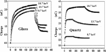
To determine the time evolution of the trapped charge, it is fundamental to calculate or to measure the influence coefficient K. In this latter case, K is estimated, either by using the method based on deflection of the primary beam, or by using the toroidal spectrometer, or even by using the influence and conduction currents measured during the discharge period (from the primary beam) [FAK 03], [FAK 04]. Figure 7.13 represents the time evolution of the trapped charge in the case of two materials (glass and quartz) having very different behaviors under irradiation.
This method can also be applied to study the charge kinetics of the insulators covered with a metallic layer under electron irradiation [JBA 02].
7.5. Conclusion
The electron irradiation of insulating materials can essentially lead to two types of effects: a charging effect and the chemical modification of the sample. These two phenomena often coexist and can interact with one another equally. The charging effect is a consequence of the electric field created by the space charge resulting from the trapping of incident electrons by the preexisting defects, and/or induced in the irradiated insulating material. The chemical modification results from the migration of mobile ions or the stimulated desorption of species, and probably implies the Auger mechanism (among other mechanisms) on the one hand and certainly the induced electric field on the other.
Both effects often depend on the crystalline structure of the sample, its geometry, its environment and irradiation conditions. Consequently, it is difficult to predict and to quantify their amplitude. Thus, the aim of this chapter was to contribute in some way to the physical understanding of these phenomena and to underline their importance on a fundamental and from a practical point of view. This chapter also sheds light on the issues associated with the irradiation of an insulator to, on the one hand remedy the latter at least partially by limiting the frequent errors of interpretation during the implementation of the analysis methods and, on the other hand benefit from it by developing techniques of electrical characterization (measurement of the charge, the time constants of charge or discharge, the surface potential and the electric field, etc.) within an SEM. These techniques are based on the mirror effect, the measurement of the Duane–Hunt limit and the measurement of both the influence and the conduction currents. A few succinct but fundamental notions concerning the secondary emission of charged insulators were also given and the importance of this phenomenon was underlined.
7.6. Bibliography
[AKK 94] AKKERMAN A., BOUTBOUL T., BRESKIN A., CHECK R., GIBREEKHTMAN A., “Low energy electron transport in alkali halides”, J. Appl. Phys. 76, p. 4656–4662, 1994.
[ALI 78] ALIG R.C., BLOOM S., “Secondary electron escape probabilities”, J. Appl. Phys. 49, p. 3476–3480, 1978.
[BEL 00a] BELHAJ M., ODOF S., MSELLAK K., JBARA O., “Time dependent measurement of trapped charge in electron irradiated insulators: Application of Al2O3-sapphire”, J. Appl. Phys., 88, p. 2289–2294, 2000.
[BEL 00b] BELHAJ M., JBARA O., ODOF S., MSELLAK K., RAU E.I., ANDRIANOv M.V., “An anomalous contrast in scanning electron microscopy of insulators: The pseudo mirror effect” Scanning 22, p. 352–356, 2000.
[BEL 01a] BELHAJ M., JBARA O., FILIPPOV M.N., RAU E.I., ANDRIANOV M.V., “Analysis of two methods of measurement of surface potential of insulators in SEM: Electron spectroscopy and X-ray spectroscopy methods”, Appl. Surf. Sci., 177, p. 58–65, 2001.
[BEL 01b] BELHAJ M., Contribution à l’étude des effets de charge dans les isolants soumis à une irradiation électronique, Thesis, University of Reims Champagne-Ardennes, 2001.
[BEN 97] BENNEWITZ R., REICHLING M., MATTHIAS E, “Force microscopy of cleaved and electron-irradiated CaF2 (111) surfaces in ultra high vacuum”, Surf. Interf, p. 387, p 69–77, 1997.
[BIG 97] BIGARRE J., FAYEULE S., PAULHE O., TRÉHEUX D., “Characterisation of the trapping of charges in polystyrene”, IEEE Tran. Dielectr Electr Insul Annual Report-Conference on Electrical Insulation and Dielectric Phenomena, p. 101–104, 1997.
[BIG 01] BIGARRE J., ATTARD C., HOURQUEBIE P., MATTALANA J., “SEM-mirror methods and application to insulating characterization”, IEEE Trans Dielectric and Electrical Insulation, 8, p. 942–952, 2001.
[BLA 91] BLAISE G., LE GRESSUS C., “Charging and Flashover induced by surface polarization relaxation process”, J. Appl. Phys. 69, p. 6334–6339, 1991.
[BLA 01] BLAISE G., “Charge localization and transport in disordered dielectric materials” Journal of Electrostatics, 50, p. 69–89, 2001.
[BRU 54] BRUINING H., in Physics and applications of secondary Electron Emission, McGraw-Hill, New York, 1954.
[BRU 83] BRUNNER M., MENZEL E,. “Surface potential measurements on floating targets with a parallel beam technique”, J Vac Sci Technol B1, p. 1344–1347, 1983.
[CAZ 90] CAZAUX J, KIM K.H., JBARA O., SALACE G., “Charging effects of MgO under electron bombardment and nonohmic behavior of the induced specimen current”, J.Appl.Phys, 70, p. 960–965, 1990.
[CAZ 91] CAZAUX J., LE GRESSUS C, “Phenomena relating to charge in insulators macroscopic effects and microscopic causes”, Scanning Microscopy, 5, p. 17–26, 1991.
[CAZ 93] CAZAUX J, in “Ionisation of solids by heavy Particles”, In NATO ASI Series B 306 Physics, BARAGIOLA, R.A. (ed.), Plenum, New York, 1993.
[CAZ 95a] CAZAUX J., “Correlations between ionisation radiation damage and charging effects in transmission electron microscope”, Ultramicroscopy, 60, p. 411–425, 1995.
[CAZ 95b] CAZAUX J., “The role of the Auger mechanism in the radiation damage of insulators”, Microsc. Microanal. Microstruct. 6, p 345–352, 1995.
[CAZ 96] CAZAUX J., “Electron probe microanalysis of insulating materials”, X-Ray Spectrometry, 25, p. 265–280, 1996.
[CAZ 99a] CAZAUX J., “Mechanisms of charging in electron spectroscopy”, J. Elect. Spect. Rel. Phen, 105, p.155–185, 1999.
[CAZ 99b] CAZAUX, J., “Some considerations on electron emission from e-irradiated insulators”, J. Appl. Phys., 85, p.1137–1147, 1999.
[CAZ 01] CAZAUX J., “About the secondary electron yield and the sign of charging of electron irradiated insulators”, European Physics Journal, AP, 15, p. 167–172, 2001.
[DIO 75] DIONNE G.-F., “Origin of secondary electron emission yield curve parameters”, Journal of Applied Physics, 46, p. 3347–3351, 1975.
[EDW 82] EDWARDs A. H., FOWLEr W. B., “Theory of the peroxy-radical defect in a-SiO2” Phys. Rev. Bulletin. 26, p. 6649–6660, 1982.
[FAK 03] FAKHFAKH S., JbARA O., BELHAJ M., FAKHFAKH Z., KALLEL A., RAU E., “An experimental approach for dynamic investigation of trapping properties of glass-ceramic under electron beam irradiation from a scanning electron microscope”, European Journal Applied Physics, 21, p. 137–146, 2003.
[FAK 04] FAKHFAKH S., Etude des phénomènes de charge des matériaux diélectriques soumis à une irradiation électronique permanente, Doctoral Thesis, University of Reims Champagne-Ardennes, 2004.
[FEI 74]. FEIGL F. J,. FOWLER W. B., YIP K.-L., “Oxygen vacancy model for the E1 center in SiO2”, Solid State Commun, 14, p. 225–229, 1974.
[FIT 74] FITTING H.J., “Transmission, energy distribution, and SE excitation of fast electrons in thin solid films”, Phy. Stat. Sol. (a) 26, p. 525–535, 1974.
[GED 99] GEDEON O, JUREK K, HULINSKY V, “Fast migration of alkali ions in glass irradiated by electons”, Journal Non-Crystalline Solids, 246, p. 1–8, 1999.
[GRI 78] GRISCOM D. L., “Defects in amorphous insulators”, J.Non-Cryst. Solids. 31, p. 241–266, 1978.
[GRI 80]. GRISCOM D. L, E’ “Center in glassy SiO2: 17O,1H, and “very weak” 29Si superhyperfine structure”, Phys. Rev. Bulletin 22, p. 4192–4202, 1980.
[GRI 81] GRISCOM D. L., FRIEBELE E. J., “Fundamental defect centers in glass: 29Si hyperfine structure of the nonbridging oxygen hole center and the peroxy radical in a-SiO2”, Phys. Rev. Bulletin, 24. p. 4896–4898, 1981.
[HAC 59] HACHENBERG O., BRAUER W., “Secondary electron emission from solids”, in Advances in Electronics and Electron Physics, MARTON, L. (ed.), vol. 11, p. 413, Academic Press, New York, 1959.
[JAR 88] JARDIN C., “Manifestation de la polarisation superficielle d’un isolant en spectroscopie d’électrons Auger et de pertes d’énergie”, Le vide, les couches minces, Société Française du Vide, No. spécial, p. 95–99, 1988.
[JAR 95] JARDIN C., DURUPT P., RIVIERE C., ROBIN M., LE GRESSUS C., “Simultaneous measurements of the surface potential and the cathodo-luminescence of Al2O3 samples” Le vide, science, technique et applications, supplément n. 275, p. 557–561, 1995.
[JBA 95] JBARA O., CAZAUX J., TREBBIA P., “Sodium diffusion in glasses during electron irradiation”, J. Appl. Phys., 78, p. 868–875, 1995.
[JBA 96a] JBARA O., CAZAUX J., REMOND G., GILLES C., “Halogen ion electric field assisted diffusion in fluorite and polyvinyl chloride during electron irradiation”, J Appl Phys 79, p. 2309–2313, 1996.
[JBA 96b] JBARA O., PORTRON B., MOUZE D., CAZAUX J., “Electron probe microanalysis of insulating materials: Monte Carlo simulations”, X-ray Spectrometry, 26, p. 291–302, 1997.
[JBA 01] JBARA O., BELHAJ M., ODOF S., MSELLAK K., RAU E.I., ANDRIANOV M.V., “Surface potential measurements of electron irradiated insulators using backscattered and secondary electron spectra from an electrostatic toroidal spectrometer adapted for scanning electron microscope applications”, Rev. Sci. Instrum., 72, p.1788–1795, 2001.
[JBA 02] JBARA O., FAKHFAKH S., BELHAJ M., CAZAUX J., RAU E.I., FILIPPOV M.V., ANDRIANOV M., “A new experimental approach for characterizing the internal trapped charge in ground coated insulators during their e irradiation” Nucl. Instrum. Methods. Phys. Res., B 194, p.302–10, 2002.
[JBA 04] JBARA O., FAKHFAKH S., BELHAJ M., RONDOT S., “Charge Implantation Measurement on Electron – Irradiated Insulating Materials by Means of a SEM Technique”, Nucl Microsc. Microanal 10, p. 697–710, 2004.
[JES 92] Numéro spécial de J. Electr. Spectrs. Rel. Phen. 59, 1992.
[JON 00] JONNARD P., BONNELLE C., BLAISE G., REMOND G., ROQUES-CARMES C., “F+ and F centers in a-Al2O3 by electron-induced X-ray emission spectroscopy and cathodoluminescence”, J. Appl. Phys, 88, p. 6413–6417, 2000.
[JOY 95] JOY D.C., “A Database on Electron-Solid Interactions”, Scanning vol.17, p. 270–275, 1995.
[KHA 82] KHAIRI I., GRAIs L., BASTAWROS A.M., “A study of secondary electron emission in insulators and semiconductors”, J. Appl. Phys., p. 5239–5242, 1982.
[LAU 99] LAURENT C., “Diélectriques solides et charge d’espace,” Tech. Ing. Traité analyse et caractérisation, D3, D 2305-1-D 2305-13, 1999.
[LEG 91] LE GRESSUS C., VALIN F., HENRIOT H., GAUTIER M., DURAND J.P., SUDARSHAN R.G., BOMMAKANTI R.G., BLAISE G., “Flashover in wide-band-gap high-purity insulators: Methodology and mechanisms”, J. Appl. Phys, 69, p.6325–6332, 1991.
[MOR 76] MORIN P., PITAVAL M., VICARIO E., “Direct observation of insulators with a SEM”, J. Physics E, 9, p. 1017, 1976.
[MOY 93] MOYA-SCIESSE D., SAMI A., MOYA G., “Characterization of charge trapping/detrapping phenomena by calorimetric measurement in charged dielectrics” in Proceeding CEIDP; IEEE Annual Report, p.104–109 & p.146–149, 1993.
[NIE 82] NIEDRIG H., “Electron backscattering from thin film”, J. Appl. Phys., 53, p.4, 1982.
[ONG 98] ONG C.K., SONG Z. G., OH K. H., GONG H., LE GRESSUS C., “Variation of the relative permittivity of charged dielectrics”, Appl. Phys. Let. 72, p.317–319, 1998.
[PEP 98] PEPIN M.P., WiNTLE J.H., “Charge injection and conduction on the surface of insulators”, J. Appl. Phys., 83, p. 5870–5879, 1998.
[RAU 96] RAU E.I., ROBINSON V.N.E., “An annular toroidal electron energy analyser for use in scanning electron microscopy”, Scanning, 18, p. 556–561, 1996.
[REI 92] REIMER L., GOLLA V., BONGELER R., KASSENS M., SCHINDLER M., SENKEL R., “Charging of bulk specimens, insulating layers and free-supporting films in scanning electron microscopy”, Optik, 92, p.14–22, 1992.
[REM 98] REMOND G., “Importance of the specimen preparation on the reliability of quantitative x-ray analysis”, Proceedings of EMAS 98, Barcelona, LIOVET, X.C, MERLET, C. SALVAT, F. (eds), p. 249–278, 1998.
[SAT 91] SATO F., GOTO K., CHIKAWA J.I., “Solid-Phase Epitaxy with X-ray irradiation to grow dislocation-free silicon films at low temperatures”, Jap. J. Appl. Phys, 30, p. 205–208, 1991.
[SCH 90] SCHWARZ S.A., “Application of semi-empirical sputtering model to secondary electron emission”, J. Appl. Phys. 68, p. 2382–2391, 1990.
[SEI 67] SEILER H., “Some problems of secondary electron emission”, Angew Z Phys. 22, p. 249–263, 1967.
[SEI 83] SEILER H., “Secondary electron emission in scanning electron microscope”, J. Appl. Phys. 54, p. R11–R18, 1983.
[SEI 84] SEILER H., “Electron Beam Interaction with Solids” in SEM, KYSER, D.F., NIEDRIG, H., NEWBURY, D.E. and SHIMIZU, R. (eds), p. 33, Chicago, 1984.
[SHI 97] SHIH A. J., YATER J., HOR C., ABRAMS R., “Secondary electron emission”, Appl. Surf. Sci., 111, p. 251–258, 1997.
[SON 96] SONG Z.G., ONG C.K., GONG H., “A time-resolved current method for the investigation of the charging ability of insulators under electron beam irradiation”, J. Appl. Phys., 79, p.7123–7128, 1996.
[STA 79] STAPELBROEK M., GRISCOM D.L., FRIEBELE E.J. AND SIGEL, G.H. “Oxygen-associated trapped-hole centers in high-purity fused silicas” J.Non-Cryst. Solids. 32, p. 313–326, 1979.
[SZY 92] SZYIMONSKI M., PORADZISZ A., CZUBA P., KOLODZIEJ J., Piatkowski P., Fine J., Tanovic L., Tanovic N., “Electron stimulated desorption of neutral species from (100) KCl surfaces”, Surface Science, 260, p. 295–330, 1992.
[TEM 06] TEMGA T., JUVÉ D., TRÉHEUX D., GUERRET-PIÉCOURT C., JARDIN C., “Conduction and trapping of electric charges in an anisotropic material after irradiation with an electron beam: application to TiO2 single-crystal” Nucl. Instr. and Meth. in Phys. Res B, 245, p. 519–527, 2006.
[VAL 94] VALLAYER B., OH K.H., TRÉHEUX D., “Charging of MgO”, Proceedings CEIDP; IEEE annual report, p. 161–166, 1994.
[VAL 95] VALLAYER B., “Développement d’une méthode de caractérisation des matériaux isolants: la méthode du miroir. Application à l’étude des propriétés de charge d’oxydes”, Thesis from the Ecole Centrale, Lyon, 1995.
[VAL 99] VALAYER B., BLAISE G., TRÉHEUX D., “Space charge measurement in dielectric material after irradiation with a 30 kV electron beam: Application to single-crystals oxide trapping properties”, Rev. Sci. Instrum 70, p. 3102–3112, 1999.
[VID 95] Le vide, science, technique et applications, Supplément to No. 275, 2th International Conference on space charges in solid dielectrics, Antibes, 1995.
[VID 01] Le vide, science, technique et applications, numéro special, 4th International conference on space charges in non conductive materials, Tours, 2001.
[VIG 85] VIGOUROUX J. P., DURAD J. P., LE MOEL A., LE GRESSUS C., GRISCOM D. L., “Electron trapping in amorphous SiO2 studied by charge build up under electron bombardment”, J. Appl. Phys. 57, p. 5139–5144, 1985.
[WEE 56] WEEKS R. A., “Paramagnetic resonance of latice defects in irradiated quartz”, J. Appl. Phys. 27, p. 1376–1382, 1956.
[WHE 64] WHETTEN N.R, “Cleavage in high vacuums of alkali halide single crystals-secondary electron emission”, J. Appl. Phys. 35, p. 3279–3282, 1964.
[WIL 73] WILLIS R. F., SKINNER D.K, “Secondary electron emission yield behaviour of polymers” Solid State Commun. 13, p. 685–688, 1973.
[WIN 97] WINTLE H.J., “Surface conduction on insulators: Analysis and interpretation of Faraday cage experiment”, J. Appl. Phys. 81, p. 2682–2685, 1997.
1 Chapter written by Omar JBARA, Slim FAKHFAKH, Sébastien RONDOT and Dominique MOUZE.