
Chapter 14
The Thermal Step Method for Space Charge Measurements 1
14.1. Introduction
The principle of non-destructive methods allowing the measurement of space charges is to detect the charges and access their distribution without modifying the electrical state of the material. The principle is therefore to make the influence charges vary at the electrodes with the aid of a non-homogeneous excitation in time and in space. The excitation can have several origins (thermal, mechanical, electrical, etc.). According to the experimentation conditions, we obtain in the external circuit linking the electrodes a signal whose analytical expression is a function of the volume charge density distribution. From this signal, the internal electric field and charge distributions can be determined after adequate processing.
Historically, a thermal stimulus was used at the Laboratoire d’electrotechnique de Montpellier(LEM). Indeed, the Thermal Step Method (TSM) has been developed at the LEM since 1986 and is based on the application of a temperature step to an insulating sample. In this chapter, after describing the principle of this technique, we shall present in detail its conditions of use, the numerical resolution methods allowing a space charge density distribution to be taken from the experimental signal, as well as the method’s recent evolutions and perspectives related to its application.
14.2. Principle of the thermal step method (TSM)
This method originally developed in 1987 [TOU 87], [TOU 90] consists of the measurement of the capacitive current which appears in the external circuit after application of a positive or negative temperature step in the vicinity of the sides of a sample. If the temperature distribution across a sample is known at any instant, it is possible to go back to both the electric field and the space charge distributions. This method presents the advantage of being applicable to thin and thick samples, whether they are plane (plates) or cylindrical (cables).
14.2.1. The TSM in short circuit conditions
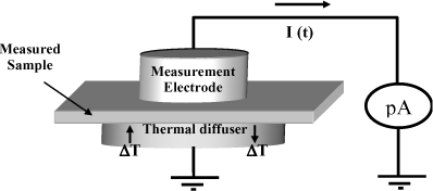
Let us consider an insulating plate of thickness d and surface S with two electrodes whose abscissae are respectively x=0 and x=d (see Figure 14.1). The material is considered homogeneous and infinitely flat ![]() thus, the electric field is considered constant in a plane parallel to the electrodes. The sample is placed in short circuit at temperature T0.
thus, the electric field is considered constant in a plane parallel to the electrodes. The sample is placed in short circuit at temperature T0.
Figure 14.1. Principle of the TSM in short circuit conditions: (a) sample at equilibrium at T0and (b) application of the thermal step

Let us consider a charge Qi situated in the insulator at a depth xi. Since the sample/electrodes/wire system is in electrostatic equilibrium, this charged plane Qi induces influence charges Q1 and Q2 at the electrodes.
The expression of the influence charges can be obtained with the aid of:
– the short circuit condition: ![]()
– the law of conservation of the electric charge: Q1 +Q2 + Qi = 0
– boundary conditions at the dielectric/conductor interfaces.
We deduce that:
If a temperature step ΔT = T − T0 is applied on one side of the sample (see the sample ΔT(x,t) = T(x,t) − T0 will generate local variations of the permittivity and the abscissae (dilation or contraction), which read (in first order):
where αε is the variation coefficient of the material permittivity with the temperature and αd its dilation coefficient.
The variations of the axis and the permittivity with temperature lead to a modification of the influence charges:
with the previously used notations and by putting:
we obtain for Q2(t) the expression:
The variation of influence charges causes the apparition of a current in the external circuit, which we call thermal step current:
If the value of the current and the spatial distribution of the temperature are known at every instant, the value of the charge Qi and its position xi can be calculated.
In general, if we define the volumic charge density by p(x) = dD(x)/dx = εdE(x)/dx on the x-axis in an infinitely flat layer of thickness dx, it can be shown by integration over the entire sample [ABO 91] [CHER 93] that the total current in the external circuit is expressed as:
where E(x) is the electric field on the x-axis and C the electrical capacitance of the sample before thermal excitation.
The thermal step current can be measured with a current amplifier. Its amplitude depends on the quantity of charges stored in the sample, the charge distribution and the material parameters. In practice, the value of the current ranges from a few pico-amperes to a few micro-amperes (for high capacitances, like those of significant cable lengths).
With the expression for the current being known, to determine E(x) we must process it mathematically. This operation requires a perfect knowledge of the derivative of the temperature ∂ΔT(x,t)/∂t at every instant and every point, which is given by the heat equation in plane geometry:
where 1/D = µc/λ is the reciprocal of the thermal diffusivity D of the material, with µ the specific mass of the insulator, c its specific heat and λ its thermal conductivity.
Further, the thermal step crosses radiator/electrode and electrode/insulator interfaces, which lead to a dampening of the temperature step which cannot be neglected during the processing of the current. To simplify the calculations, we can use an “equivalent thickness” model, i.e. we consider that the total thickness x1, of different interfaces and average reciprocal thermal diffusivity 1/D1, is equivalent to a thickness x0 with the same reciprocal thermal diffusivity 1/D0 as the insulator. The integral limits (0 and d) can thus be replaced by x0 and x0+d (the electric field between 0 and x0 is null):
In pratice (see Figure 14.2), the thermal step is created by a sudden circulation of a cool (or warm) liquid in a radiator in contact with the sample (or by a transient current which heats up a resistive material under the sample [ODI 00]). The electrodes are connected through a current amplifier. This latter is linked to a computer which records the signal and does the numerical processing. After the execution of a measurement, the sample can be brought back to room temperature by using a 25°C liquid, and the experiment can thus be repeated.
Similar equations and an analogous experimental device [SAB 91], [SAN 94] are used in the case of power cables.
The TSM in short circuit conditions reports on the residual static state of charges in a material before and after the application of the applied electric field. However, to remain close to the service conditions of insulated systems and for a better understanding of phenomena appearing when the external electric field is applied, the TSM was designed to take measurements under an applied electric field [NOT 01a]. Furthermore, the measurements under voltage can bring useful information for the calibration of the technique. This principle can also be directly used for industrial applications.
14.2.2. Evolution of the TSM for measurements under a continuous applied electric field
To make measurements under a continuous electric field, the device described in Figure 14.2 presents two major disadvantages:
– the current amplifier must not be in contact with the high voltage source;
– if a set up with the current amplifier placed between the sample subjected to a high voltage and the ground is used (as, for example, for conduction current measurements), the conduction and polarization currents are likely to mask the thermal step current.
A solution to these problems is to use a “compensation sample”, with identical dimensions to the measurement sample, placed opposite to this latter. By connecting one side of the compensation sample to the current amplifier and the other to the measurement sample via an electrode, a “double capacitor” is created. A potential can thus be applied to the central electrode and the thermal step to the measured sample. The signal is then acquired through the compensation sample.
The use of two identical samples brings the advantage of compensating for the polarization and transient conduction currents which can appear under strong fields; the measured current is thus exclusively due to the internal electric field of the measured sample.
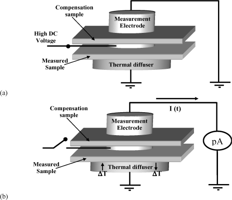
The “under field” measurement is thus realized in two stages (see Figure 14.3):
– during the electrical conditioning, the potential is applied to the central electrode and the current amplifier is short circuited (the samples constitute two electrical capacitances placed in parallel with respect to the voltage source (see Figure 14.3a).
– in order to avoid the transport of influence charges to the electrodes through the high voltage source, this latter must be disconnected during the measurement (see y thermal excitation of the studied sample (in contact with the thermal diffuser), while the current amplifier is connected to the compensation sample (two samples in series with the current amplifier, in short circuit conditions).
The thermal step current in the external circuit is given by:
where C2 is the capacitance “seen” by the current amplifier.
During the measurement, both samples are in series. If they are identical, C2=C/2. In the absence of applied voltage, the TSM current must be half of that obtained in short circuit conditions with the thermally excited sample (where C2=C).
For weak applied fields, the field can be considered constant in the material (with no injected charges): E(x)=Ee=V/d, where V is the applied voltage. In this case, the signal becomes directly proportional to V:
[14.12] ![]()
This current can be used as a calibration current in the mathematical processing of the TSM signal.
If thasurement sample already contains space charges giving a residual field Er(x), and an external electric field is applied to the material (Ee=V/d which does not modify the distribution of space charges), the total field in the sample becomes E(x)=Er(x)+Ee.
Equation [14.11] can then be written in the form:

where I0(t) is the current due to the residual space charges and If(t) the current due to the external field.
14.2.3. Calibration: use of measurements under low applied field for the determination of material parameters
Let us consider an insulating sample which contains a certain quantity of space charges inducing a residual electric field Er(x). If the sample is subjected to an external field Ee =V/d which does not cause any charge injection and does not modify the charge distribution in the sample, the measured TSM current, denoted as I+, has an expression identical to equation [14.14]
The application to the sample of an external electric field of similar value Ee but of opposite polarity gives a current I as follows:
The difference between the currents obtained by both measurements is then:
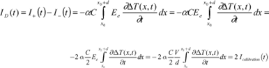
where Icalibration (t) (calibration current), which is a function of the applied voltage and the insulating material parameters, is defined by:
The theoretical expression of the thermal stimulus is (in the case of only one thermal source):
The integral K(t) is therefore:

Thus, the temporal knowledge of K(t) allows the parameters 1/D and x0 to be determined, necessary for the mathematical processing of the TSM signals.
14.3. Numerical resolution methods
The TSM was one of the first techniques to give values for electric fields and space charge densities in polyethylene plates and in insulated cables. During the last few years, several calculation techniques for the field have been developed. They have followed the evolution of calculation software available on the market. In the 1980s, laborious programming (in Basic, Fortran, etc.) was necessary, whereas today performance algorithms are included in the laboratory software, making the calculations easier and noticeably improving the presentations.
The fundamental problem, as in all other indirect methods using a thermal stimulus or based on pressure, takes the form of an integral equation.
In the case of insulating plates or films with a thicknesss from a few tens of microns to several millimeters, the TSM determines the electric field E(x) according to Equation [14.10]. The source of temperature - due to the “sudden” arrival of a cold or hot liquid in a small radiator – is supposed to provide a temperature step at x=0 (origin). The resolution of the heat equation, by assuming the temperature source placed near the side of the sample in contact with the radiator, gives the spatiotemporal expression for the thermal stimulus in the sample, corresponding to equation [14.18]. This stimulus, which has the appearance of a wave, propagates fairly slowly in the insulator. Its most advanced position is called A(t).

If we now consider that there is a second source of temperature at the end of the sample, corresponding to a second massive electrode situated at the x0+d axis and therefore maintained at room temperature during the experiment, then the resolution of the heat equation gives, for the stimulus:
with ![]()
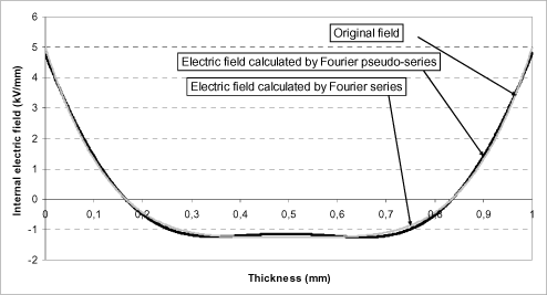
This form of the stimulus leads us to express the electric field in the form of a Fourier series:
Unfortunately, this natural form could only give the electric field in part of the sample, since E(x)=0 in x=L, which is not realistic. We have therefore preferred to use a more general form, which has turned out efficient, in the form of a Fourier pseudo-series, non-null in x=L.
In this processing by even and odd Fourier pseudo-series, we develop E(x) in cosine and sine series, by taking the center of the sample as the origin for the total thickness:
where ll = xo+d/2.
By inserting equation [14.22] into equation [14.10], then by integrating, it is possible to obtain by fitting or by Laplace transform 7 to 14 terms of the Fourier pseudo-series.
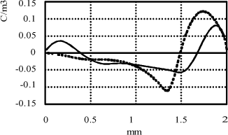
An example of resolution is shown in Figure 14.5. Good results were also obtained on cables, with an important noise percentage (5–10%) [NOT 07]..
Figure 14.5. Example of internal electric field distributions obtained for the mathematical processing by Fourier pseudo-series
14.4. Experimental set-up
This section concerns the manner in which the TSM current measurement is made. The cases of both plate-type materials and cable-type components are addressed.
14.4.1. Plate-type samples
As can be deduced from equation [14.8], the measured amplitude of the TSM current principally depends on five parameters: the thermal diffusivity of material D, the relative variation of the electric capacitance with temperature α, the electrical capacitance of sample C, the internal electric field E(x) and the amplitude of the thermal step ΔT0. It is then evident that the current amplitude will get bigger as the sample capacitance and the step amplitude get bigger. The effect of the combination of these two parameters is that the thickness characterizable by the TSM is not really limited, but depends on the electrical capacitance of the sample and on the ability of the thermal source to transfer effectively the thermal step to the sample. In other words, the thicker the sample, the more powerful the thermal source must be. However, it is necessary to avoid temperature rises which could generate undesirable thermally stimulated discharges. In general, the use of negative thermal steps is preferable, because a cooling of the sample does not affect its internal electrical state (it is also necessary to check for each studied material that no phase change appears in the range of temperature used).
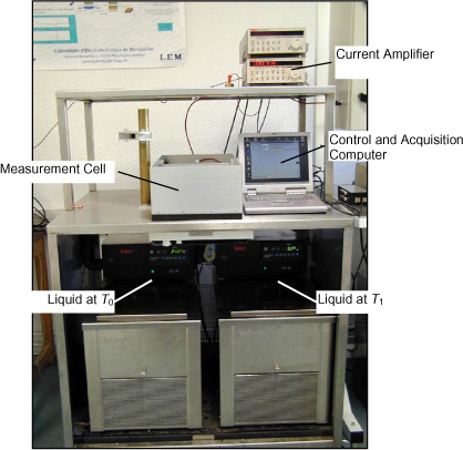
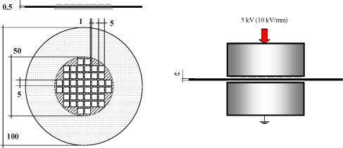
The measurement bench of the TSM for the characterization of plate-type samples consists of two cryo-thermostats (reservoirs filled with a mixture of water and ethanol, temperature regulated) permitting the mixture of refrigerant liquids to circulate in a radiator (for thermal step generation, then back to temperature after the measurement of the signal).
The circulation of the calo-carrier liquid in the radiator is generated by a set of electrovalves controlled by a computer. The radiator is situated in a measurement cell ensuring the role of a Faraday cage (see Figure 14.6). The measurement of current, during the application of the thermal step (generally negative, as we have previously described it, in the case of insulating samples: with the circulation of a liquid at −5°C for a few seconds), is realized with the aid of a Keithley 428 current amplifier. The thermal step amplitude must not modify the electrical characteristics of the material (amplitude of the smallest possible step, generally of the order of 20 to 30°C, in the service domain of the material).
Figure 14.7 below presents the setup used in the case of metal-oxide-semiconductor (MOS) structures for microelectronics. The MOS samples are placed on a radiator producing the thermal step. A needle (connected to the current amplifier input) is placed on the gate of the MOS structure, the rear side of the sample (below the Si substrate) being connected to the ground. The current amplifier used offers the possibility of applying a voltage to the sample during the measurement of current (bias voltage VBIAS). This setup thus allows the charge evolution in the oxide to be followed during different polarization regimes of the structure. To avoid humidity issues, the applied thermal step is positive in the case of MOS structures (making sure not to modify the charge carrier density in the silicon during the measurement).

14.4.2. Power cables
The TSM can also be applied to power cables in short circuit conditions and under an applied DC field. In each, case the temperature step can be generated owing to the circulation of a calo-carrier or frigo-carrier liquid in a thermal diffuser adjusted for the geometry of the cable. (The application of a negative thermal step is generally preferred). This technique, known as “outer cooling”, allows a localized analysis of the insulating part of the cable wrapped up by the diffuser.
The thermal step can also be generated by the passage of a strong current in the central core of the cable (temperature rise generated by the Joule effect). This technique, known as “inner heating”, allows a global analysis of the insulation on the cable length.
14.4.2.1. Measurements in short circuit conditions
The equipment dedicated to experiments in short circuit conditions on cables by the external cooling technique is made up of a “cooling” part and of an “acquisition” part. This equipment (see Figure 14.8) is analogous to the one used for flat samples, except for the thermal diffuser, which is a cylindrical cover wrapping the cable (see Figure 14.9.a and b).


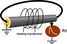
The conductor heating technique (central core), composed of a part known as “heating” and a part known as “acquisition”, uses a coil of inductive heating (4) which wraps up the cable, constituting the primary part of a heating transformer which has as its secondary part, the core of the measured cable. The heating time is controlled with the aid of two controlled rectifiers, or thyristors, mounted on opposite sides (12) (seeFigure 14.11b). The heating time is calculated beforehand in order to generate a thermal step sufficiently important to reveal the electric charges present in the entire insulating thickness of the cable. The command order for the controlled rectifiers is generated remotely by software integrated in the “acquisition” part. This command system permits the heating duration of the cable core to be managed. The acquisition part is similar to that of the external cooling part, but the command software controls the thyristors, not an electrovalve system. The “acquisition” part is made up of a computer, a GPIB card (8) and an acquisition board fitted with digital and analog input/output ports (9).
14.4.2.2. Measurements under applied electric field
As in the case of flat samples (see section 14.2.2), the experiment under applied electric field requires the use of two identical cables (the same electrical capacitance and dimensions) whose external electrodes are insulated from one another [NOT 01a]. This “under field” measurement technique has been installed at the Nexans-France site in Calais since the year 2000.
First, the cables are subjected to an electric field via a high voltage relay (2), the current amplifier (3) fitted with a GPIB interface in short circuit (see Figure 14.10.a). The second stage consists, in the case of external cooling (see Figure 14.10.b), of measuring a current due to the application of a thermal step generated by a cryo-thermostat (5) owing to a heat exchanger (6) – a temperature diffuser – wrapping up a part of the measured cable to a length of 10 to about 100 cm.


The heat exchanger (connected to the ground) is placed on the test cable (A); a measurement is made with the aid of the current amplifier placed between the external semi-conductor of the other cable (B) and the ground.
In the case of inner heating, the thermal step is generated by the injection of a strong current to the central core of the cable to be measured; the measurement is made on the compensation cable. During the current measurement, the voltage source (1) must be disconnected from the central core of the cables because the system must imperatively remain insulated during the acquisition of the signal. This imposes the use of a remote high voltage switch (2), controllable from the command desk (10).
Both “external cooling” (see Figure 14.11.a) and “inner heating” (see Figure 14.11.b) techniques use the same equipment as for the short circuit measurements. Only the algorithms of command software are different, in order to additionally command the high voltage switch and the short circuit relay (11) of the current amplifier. The acquisition of the signals remains unchanged.


Figure 14.12. Experimental equipment for measurements on cables under electric and thermal gradient installed at the Nexans-France site in Calais. A: measurement cable; B: compensation cable; 1: HV DC source; 2: H relay; 3: current amplifier; 4: heating; 5: thermal sources; 6: thermal diffuser; 7: computer; 10: command desk

14.5. Applications
14.5.1. Materials
14.5.1.1. Influence of molar weight and cooling rate on the presence of space charges in polyethylene [TOU 98]
In order to study the appearance of space charges in polyethylene (PE) after manufacturing, several samples were made by press-moulding PE ribbons. Four samples in the form of 2mm thick plates with similar density (~960 kg/m3) were made according to the same procedure, but with different molar weights (Mw). The characteristics of the samples are presented in Table 14.1.
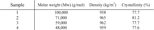
Figure 14.13 shows that all the space charge distributions are symmetrical and the space charge levels seem directly related to the molar weight. A strong molar weight implies a strong level of space charge. Further, the microscope observation of samples with the same density but different molar weights (see Figure 14.14) shows that a high molar weight induces small spherulites. We can infer from this that the space charge level is inversely proportional to the size of the spherulites. Indeed, this idea agrees with the theory of Ikezaki et al. [IKE 94], who showed that space charges are principally trapped in the core and at the periphery of spherulites, which are amorphous regions rich in defects and impurities.
During the manufacture of a PE sample, we have also made an asymmetric cooling. Thus, a side of the sample was rapidly cooled towards room temperature (cooling rate of 40°C/min, using a water cooling system), while the the other side was left to cool down naturally (at a rate of 1°C/min, imposed by thermal inertia of the moulding system). The experimental results give an asymmetric space charge distribution for asymmetric cooling (see Figure 14.15). The side which was rapidly cooled presents more space charges than that cooled more slowly. A microscope visualization of samples shows that the cooling rate also has an influence on the size of spherulites (see Figure 14.14).
Figure 14.13. Space charge distribution on PE samples after manufacturing (thin line: sample 1; dotted line: sample 2; dashed line: sample 3; bold line: sample 4)

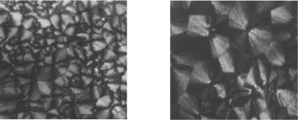
Figure 14.15. Influence of the cooling rate on space charges in PE (continuous line: symmetrical cooling, dotted line: asymmetric cooling)
The results presented show that press-moulded PE plates contain space charges just after manufacture. The development and the charge trapping are then produced during manufacturing whilst the material is being solidified (the thermal gradient present in the sample during cooling could cause the transit of negative charges towards the core of the sample).
14.5.1.2. Revealing the heterogenity of composite materials (charged epoxy resin)
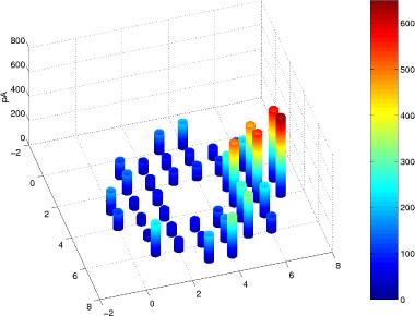
Composites are heterogenous materials by definition. The aim of this study was to verify their behavior regarding the accumulation of space charges when they are subjected to a strong electrical and thermal constraint which was also heterogenous. In order to verify these heterogenities, the surface of a 1mm thick charged epoxy resin sample was divided into 40 pins of 25 mm2, arranged in a circular shape of diameter 5cm (see Figure 14.16.a). After an electrical conditioning (10 kV/mm, 80°C, 22 hours) carried out with two electrodes of diameter 5cm placed on both sides of the sample (see Figure 14.16.b), each pin was analyzed by the TSM: the results obtained are presented in Figure 14.17, where the maximal values of TSM signals collected on the 40 pins spread out on the surface of the electrode are represented.
The results of this study allow the observation of heterogenities as a function of the different analyzed zones (pins). Essentially, three zones presenting different volume densities of residual space charges can be seen: a central zone showing a rather weak average level, a peripheral zone showing a higher average level, and a zone of the order of 25% of the tested surface showing a clearly more important average level (amplitude of the TSM currents up to 6 times higher; remember that the amplitude of the TSM signals is a function of the space charge density).
Figure 14.17. TSM current amplitude as a function of the position of the pins – Revealing the heterogenity of an epoxy resin sample
Analogous studies were also made on other samples and components, and showed that the heterogenities of a polymeric material strongly depend on the sensitivity of the measurement tool which is used [CAS 03].
14.5.1.3. Evolution of space charges in materials for cables subjected to an alternative electrical constraint (50 Hz)
If direct current is considered to be the future of high voltage power transport, the crushing majority of high and medium voltage cables with synthetic insulation are used today for AC transport (50 Hz). When we know that the required lifespan for this type of component reaches 40 years, we can easily understand the importance of the subject. If the accumulation of space charges and their role in the degradation process are clearly established in the case of a solid insulator subjected to a strong DC field, a few points on this subject are still to be cleared up when the material is subjected to an alternative constraint. Notably, the question: “space charge: cause or effect of the degradation under alternative field?” has yet to be solved.
However, whatever the envisaged degradation mechanisms, it is clear that space charge measurements give important indications concerning the state of an insulator subjected to an alternative constraint. Indeed, the gradual accumulation of charges in deep traps (greater than 1 eV [NOT 01b]) necessarily means a multiplication of these latter, which corresponds to an increase in the number of morphological defects and to chemical bond breaks. In this sense, we talk about “static” charges, since they remain trapped for a long time after the stress has been turned off, while the “dynamic” charges, weakly trapped, recombine with the inversion of the field. Revealing the static charges is quite difficult, especially if the material is not very “old”, since their density is relatively weak because of the alternative nature of the field. Incidentally, most techniques cannot detect them with sufficient precision. Owing to its sensitivity, the TSM allows these accumulations to be detected and their evolution to be followed, which can be estimated as parallel to the degradation process [AGN 03].
Figure 14.18. Charge density distribution in cross-linked polyethylene (PR) subjected to a 40 kV/mm AC field (50 Hz) for 15 days at different temperatures [NOT 01b]

Figure 14.18 shows results obtained in plane samples of cross-linked polyethylene used in high voltage cables. We see here the “static” charge distribution (deeply trapped), with a symmetric and bilateral shape (related to the alternative nature of the constraint). Figure 14.18 also shows that the accumulation of alternative charges is not an increasing function of the temperature, but can present maxima for particular values of the thermal constraint (the most important accumulation is at 60°C in the case presented). These values of the temperature depend on the structure and on the initial morphology of the material, as well as on their modification in time.
We can use the total absolute value of the deeply trapped charge QABS = |Q+| + |Q−| in order to follow the evolution of the insulator. This amplitude can thus be considered as the image of the concentration of deep apparent defects (filled traps) created during ageing. The evolution of the apparent defect density in high voltage cables subjected for several thousand hours to strong constraints is presented in Figure 14.19, where we observe a global upward trend in ageing over time. This increase is very strong for conditionings carried out at 145 kV and 325 kV, as well as for the conditioning at 225 kV up to 5,000 h. Because the measurements were made on sections periodically cut from loops conditioned during several thousand hours, the observed decrease at 225 kV after 5,000 h is related to the non-homogenity of one of the cable sections, as was shown in [CAS 03]. An important increase of the number of filled deep traps is also observable when the applied voltage increases, especially if we compare the cables conditioned at 145 kV with the others. The application of the stress for several thousand hours has therefore caused structural changes in the insulation, which manifest themselves by an increase in concentration of deep traps; this latter could be used as a marker for the evolution of the cable.
Figure 14.19. Evolution of the apparent concentration of filled deep traps in high voltage cables (90 kV) subjected to different voltages, at 90°C [NOT 03]

14.5.2. Components
14.5.2.1. Monitoring of the internal electric field of a cable subjected to electrical and thermal stress
Electric field monitoring in the insulation of a DC cable in service conditions can represent an essential stage for the assessment of the long-term behavior of the cable. Such monitoring was carried out on a 20 m long cable with an insulating thickness of 5.8 mm, by using the thermal step bench from the Nexans-France site in Calais.
Several test conditions were applied to the cable; the results presented in Figure 14.20 were obtained for an ageing performed under electrical and thermal gradients according to the following conditions: −85kV DC and 80°C on the central core of the cable. TSM measurements have been regularly made by using the equipment described in section 14.4.2.2 (see Figure 14.12) to observe the evolution of the internal electric field during the test period [CAS 05].
Figure 14.20. Evolution of the internal electric field measured in the DC cable insulation (−85 kV DC, 80°C applied on the conducting core situated on the left of the figure)

The electric field distributions presented in this figure are strongly distorted with respect both to a Laplace theoretical distribution (capacitive distribution assumed in the absence of space charge and thermal gradient) and to a “resistive” repartition (theoretical electric field in an insulation subjected to electrical stress and thermal gradient, in the absence of space charge) [COE 01]. In some areas of the cable insulation, the measured electric field is two times higher than the theoretical values because of the presence of space charges.
The trend of the field repartition to switch toward a resistive-like curve after 7 days of testing must be underlined, because such an inversion, theoretically demonstrated, had never been experimentally observed before. The internal field measured near the conductor thus tends to pass from the Laplace field to the minimum value predicted by the resistive model. Further, the field distortion is more important than predicted by the resistive model, more particularly in the vicinity of the semiconducting shield. This behavior underlines the complex dynamics of space charges, notably by taking into account the injection phenomena. Despite the field model which seems established beyond 11 days of testing, an evolution is still apparent after 42 days under constraint, thus suggesting that the equilibrium state is still not reached.
14.5.2.2. Monitoring of the ageing of micaceous composite insulation from a power alternator winding
This work aimed at monitoring the evolution of space charges in a 2 mm thick insulator from a stator winding of a high power AC machine. For this purpose, the sample was subjected to accelerated AC ageing under 18 kV RMS voltage (50 Hz) applied on the conductor at room temperature, i.e. twice the service voltage (9 kV/mm average electric field). Several measurements were made during ageing, until breakdown occurred [CAS 02].
Figure 14.21. Evolution of the TSM current amplitude in the insulation of a high power AC machine submitted to AC stress

Figure 14.21 shows an increase of the TSM current amplitude during ageing, the breakdown occurring after 1,180 hours of ageing. In these ageing conditions, 936 hours correspond to 70% of the lifespan of the sample.
The space charge density profiles presented in Figure 14.22 show an increase of the levels with the ageing time. We also notice negative charge injection from the copper (on the right in Figure 14.22), and a migration of negative charges towards the outer electrode after breakdown (on the left in Figure 14.22).

14.5.2.3. Characterization of Metal-Oxide-Semiconductor (MOS) structures for micro and nanoelectronics
Providing that the sample capacitance and the thermal step amplitude are sufficient, there is in principle no restriction concerning the thickness the TSM is able to characterize. Although initially developed for the study of thick insulators, the technique could thus be adjusted for a large spectrum of thicknesses and geometries, and notably for thin layers, such those of semi-conducting components.
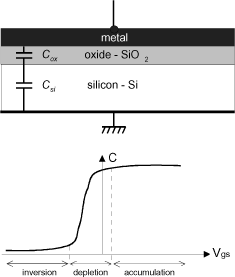
We recall that a MOS capacitance (the basis of most electronic components) is composed of an n or p doped silicon substrate, from which a silicon dioxide (SiO2) layer is grown, most often by thermal oxidation (see Figure 14.23). When a variable voltage (noted further Vg or Vgs) is applied to the gate (electrode in contact with the SiO2), the overall capacitance of the structure varies proportionally to the extension of a charge zone at the oxide/semi-conductor interface, which is comparable to a variable capacitance in series with the oxide. For a value of the voltage Vg called the threshold voltage, the thickness of the space charge zone in the semi-conductor becomes so high that the total capacitance of the structure collapses, allowing the switching of the component which integrates the MOS structure from the off-state to the on-state, or vice-versa (see Figure 14.23).
To illustrate the functioning of a MOS capacitance, let us first envisage the case of an “ideal” component. For such a structure, we suppose that:
– the doping of the semi-conductor is such that the work functions of the metal and the semi-conductor are identical;
– there are no traps at the interface between the oxide and the semi-conductor;
– there are no charges in the oxide, the insulator is perfect.
As previously evoked, the capacitance of the structure is a grouping in series of the semi-conductor’s capacitance CSi and the insulator’s capacitance Cox: 1/CMOS = 1/Cox + 1/CSi. The oxide’s capacitance is independent of the voltage Vgsapplied to the structure: Cox = ε0εoxS/dox, with ε0 the vacuum permittivity, εox the relative permittivity of the oxide, S the surface of the gate and dox the thickness of the oxide. On the other hand, the capacitance of the Si is determined by the apparition of a space charge zone in the semi-conductor, which varies as a function of Vgs.
Three regimes are possible:
– accumulation of majority carriers;
– depletion of majority carriers;
– inversion (the density of minority carriers becomes greater, in the neighborhood of the SiO2-Si interface, than the density of majority carriers).
However, in real structures, the oxides cannot be exempt from charges. It is well known that the accumulation of charges in the oxide and the increase of traps at the oxide/semi-conductor interface strongly affect the structure, first by moving its switching threshold (so leading to a bad functioning of the device), then by reducing the lifespan of the oxide. The charge measurement (especially that of interface charges) is a major issue for the improvement of the reliability of semi-conducting devices. However, because of the shallowness of the interface traps, it may be difficult to quantify them with traditional techniques.
In the following figures, thermal step currents are presented, measured for several values of the gate voltage Vg for n- and p-doped substrates 1015 cm−3. Capacitance-voltage (C-V) measurements performed on the same samples are also shown.
The thermal step currents permit the three functioning regimes of the structures to be identified. Thus, the accumulation regime (which corresponds, in the case of ideal MOS capacitances, to a negative gate voltage for a p-substrate and a positive one for an n-substrate) is defined by a slight reduction of the thermal step current amplitude when the gate voltage increases. We also note that the currents are opposite for n-substrate and p-substrate structures: this is due to the opposite signs of charges near the Si surface in both types of structures. Thus, in accumulation, the charge at the Si-SiO2 interface is negative for an n-type substrate and positive for a p-type substrate.
The same reasoning can be made for the inversion regime. In this case, the charge signs in the substrates, i.e. the TSM current signs, are reversed: the charge at the interface is positive for the n-substrate and negative for the p-substrate.
The depletion regime is characterized by a very fast variation of the thermal step current amplitude, while the gate voltage Vg does not vary much; this variation is related to the very rapid variation of the space charge zone width in the Si. The space charge zone in the Si induces a collapse of the total capacitance of the structure observed by C(V). This zone reaches a maximum for the threshold voltage VTH. From this threshold, the minority carriers appear at the Si-SiO2, interface causing a sudden increase of the capacitance until its accumulation value Cox.
Figure 14.24. Thermal step currents obtained with the TSM on both types of MOS structures with gate oxide thickness of 120 nm (a–c with n-type substrate; d–f with p-type substrate)

The measurement of the structure capacitance made by C(V) at high frequency (1 kHz) does not permit the contribution of minority carriers to be revealed. On the other hand, this rise is observed at low frequency (20 Hz) C(V) and especially with the TSM. Indeed, the TSM currents reach, in inversion, quasi-equivalent amplitudes to those of accumulation currents (but of an opposite sign).


Figure 14.27. Amplitude of thermal step currents (Imax) as a function of the gate voltage (Vg) on a p-type substrate MOS capacitance

Figure 14.28. Amplitude of thermal step currents (Imax) as a function of the gate voltage (Vg) on an n-type substrate MOS capacitance

The representation of the thermal step currents amplitude (Imax) as a function of the gate voltage (see Figures 14.27 and 14.28) permits the current maximum (corresponding to the flatband) and its minimum (threshold voltage) to be spotted accurately, and for them to be compared with the estimations given by C(V) (see Tables 14.2 and 14.3).
We observe a good correlation between both characterization types; however, the values measured with both techniques are not identical.


In fact, the threshold values obtained with the TSM and the C(V) could only be identical if the measurements of C(V) were made at the same frequency as that of the TSM, i.e. at a very low frequency (0.1 Hz). This means that the TSM permits to charges to be found that the C(V) cannot reveal, even at a frequency of 20 Hz. These are notably the weakly trapped interface charges, which do not appear with the C(V). The differences between both methods are stronger when the interface state density increases. We must note that the contribution of the thermal step technique is more important when the interface state density is high, and notably in the case of irradiated components, as it was shown in [FRU 06]. In this case, the use of the TSM permits all of the interface charges to be easily revealed, while the use of the C(V) requires fairly tricky calculations and may not allow all of these states to be measured.
It is therefore possible to calculate the total charge in the structure and, by measurements at different voltages, to separate the contributions of different carriers. For example, at the removal of the thermal step current (Imax = 0), we can calculate the charge quantity in the structures Q0 = −CoxVg. For both previous structures, we obtain:
Table 14.4. Values of Q0 calculated for Vg[IMax(Vg) ≈ 0]
| N-type substrate | P-type substrate | |
|---|---|---|
| Vg [IMax(Vg) ≈ 0] | 0.8 V | 0.3 V |
| Q0 | − +4.4.10−9 C | − +1.65.10−9 C |
For IMax≈0, the inversion is already made in the n-type substrate MOS structure, because the charge is positive. On the other hand, for the p-type substrate MOS structure, the charge quantity at the interface has decreased compared to the flat band regime, but the inversion has not yet appeared.
Studies undertaken on gate insulator MOS capacities with even weaker thicknesses, up to 1 nm, have shown that the TSM can be applied on this type of component, allowing the different charges existing in the structure to be evaluated, and notably the interface charges [FRU 06]. This allows the use of this technique as a characterization method in the micro and nanoelectronic domain to be envisaged, in the near future.
14.6. Conclusion
The thermal step method for measuring space charges was invented in 1986. Since then, the technique has not stopped evolving and the different studies and researches led for the last few years have made it a renowned non-destructive characterization technique, both by the academic community and by industry.
The latest advances permit us to catch a glimpse of numerous studies allowing a better understanding of the phenomena of appearance and development of space charges in solid insulating materials subjected to various stress. Today, characterizations of insulators under continuous electric fields and thermal gradients are realizable, both in a laboratory and in industry, in close to operational conditions (for measurements applicable to materials and components).
The progress achieved and the industrial collaborations made have thus resulted in the technological transfer of this method to the cable industry. The use of this type of testing technique in real conditions should allow the processes leading to insulation ageing being fully understood.
14.7. Bibliography
[ABO 91] ABOU DAKKA M., Mesures de charges d’espace dans divers polymères par la méthode de l’onde thermique, Doctoral Thesis, University of Montpellier 2, 1991.
[AGN 03] AGNEL S., PLATBROOD G., TOUREILLE A., “Study of AC electrical and thermal ageing of XLPE polyethylene by space charge measurements”, Proceedings of the Jicable 2003 IEEE International Conference on Insulated Power Cables, Versailles, p. 479–484, 2003.
[CAS 02] CASTELLON J., MALRIEU S., TOUREILLE A., “Measurement of space charge evolution in insulation of electrical machine winding: correlation with AC ageing”, Proceedings of the INSUCON 02 Conference, p. 165–170, 2002.
[CAS 03] CASTELLON J., MALRIEU S., NOTINGHER Jr P., TOUREILLE A., BECKER J., DEJEAN P.M., JANAH H., MATALLANA J., VERITE J.C., “On site measurements on HV cable loops as part of the ARTEMIS project”, Proceedings of the Jicable 2003 IEEE International Conference on Insulated Power Cables, p. 714–719, 2003.
[CAS 05] CASTELLON J., NOTINGHER P., AGNEL S., TOUREILLE A., MATALLANA J., JANAH H., MIREBEAU P., SY D., “Industrial Installation for Voltage-On Space Charge Measurements in HVDC Cables”, Industry Applications Conference, 40th IAS Annual Meeting, Conference Record of the 2005, Hong Kong, p. 1112–1118, vol. 2, 2005.
[CHE 93] CHERIFI A., Contribution à l’étude des charges d’espace dans les polymères isolants utilisés en haute tension. Améliorations de la méthode de l’onde thermique, Doctoral Thesis, University of Montpellier 2, 1993.
[COE 01] COELHO R., ALADENIZE B., GUILLAUMOND F., “Charge build-up in lossy dielectrics with induced inhomogeneities”, IEEE Transactions on Dielectrics and Electrical Insulation, vol. 4, no. 5, p. 477–486, 1997.
[FRU 06] FRUCHIER O., Etude du comportement de la charge d’espace dans les structures MOS. Vers une analyse du champ électrique interne par la méthode de l’onde thermique, Doctoral Thesis, University of Montpellier 2, 2006.
[IKE 94] IKEZAKI K., YAGISHITA A & YAMANOUCHI H., “Charge trapping in spherulitic polypropylene”, Proceedings of the 8th International Symposium on Electrets, Paris, France, p. 428–433, 1994.
[NOT 01a] NOTINGHER P. Jr, AGNEL S., TOUREILLE A., “The Thermal Step Method for Space Charge Measurement under Applied DC Field”, IEEE TDEI, vol. 8, no. 6, p. 985–994, 2001.
[NOT 01b] NOTINGHER P. Jr, TOUREILLE A., SANTANA J., ALBERTINI M., MARTINOTO L., “Study of Space Charge Accumulation in Polyolefins Submitted to AC Stress (50 Hz)”, IEEE TDEI, vol. 8, no. 6, p. 972–984, 2001.
[NOT 03] NOTINGHER P. Jr, TOUREILLE P., AGNEL S., DIDON N., CASTELLON J., MALRIEU S., “Survey of space charge evolution in high voltage cables sublmitted to AC voltage as part of artemis project”, Conference Proceedings of the Jicable 2003 IEEE International Conference on Insulated Power Cables, Versailles, France, p. 468–472, 2003.
[NOT 07] NOTINGHER P. Jr, TOUREILLE A., AGNEL S., CASTELLON J., “Determination of Electric Field and Space Charge in the Insulation of Power Cables with the Thermal Step Method using a New Mathematical Processing”, IEEE Transactions on Industry Applications, vol. 45, no. 1, p. 67–74, 2009.
[ODI 00] ODIOT F., Mesures de charges d’espace dans le SiO2 par la méthode de l’onde thermique: application aux technologies MOS, Doctoral Thesis, University of Montpellier 2, 2000.
[SAB 91] SABIR A., Sur une nouvelle méthode de mesure des charges d’espace dans les câbles haute tension, Doctoral Thesis, University of Montpellier 2, 1991.
[SAN 94] SANTANA J., Mesures de charges d’espace dans les câbles de transport de l’énergie électrique, Doctoral Thesis, University of Montpellier 2, 1994.
[TOU 87] TOUREILLE A., “Sur une méthode de détermination de la densité de charges d’espace dans le polyéthylène”, Proceedings of the Jicable 87 IEEE International Conference on Insulated Power Cables, p. 89–103, 1987.
[TOU 90] TOUREILLE A., SABIR A., REBOUL J.P., BERDALA J., MERLE P., “Determination of space charge densities in a high voltage thick insulated cable using the thermal step technique”, Revue de Physique Appliquée, vol. 25, no. 4, p. 405–408, 1990.
[TOU 98] A. TOUREILLE, P. NOTINGHER Jr, N. V ELLA, J. CASTELLON, S. MALRIEU, S. AGNEL, “The Thermal Step Technique: An advanced method for studying the properties and testing the quality of polymers”, Polymer International, vol. 46, no. 2, p. 81–92, 1998.
1 Chapter written by Alain TOUREILLE, Serge AGNEL, Petru NOTINGHER and Jérôme CASTELLON.