
Chapter 20
Semiconducting Organic Materials for Electroluminescent Devices and Photovoltaic Conversion 1
20.1. Brief history
During the last 50 years, polymers have held an increasingly important place amongst dielectric materials. They are light, easy to process, and their physico-chemical properties can be modified by well-established techniques of organic chemistry. Although less present in industrial applications, semiconducting organic materials offer the same advantages as their inorganic counterparts. The strong interest aroused by organic electronics since the end of the 1980s recently led to the commercialization of organic displays. Nevertheless, more work needs to be put into research, particularly to achieve the production of flat screens and to improve the performances of organic photovoltaic cells. The organic semiconductors which constitute the active layers of these components are generally listed in two categories: polymers and materials with low molar mass, or “small molecules”.
The phrase “organic semiconductor”, applied today to different types of materials, was initially applied only to certain molecular crystals (naphthalene, anthracene, etc.) presenting properties similar to inorganic semiconductors. In particular, the electroluminescence of anthracene was studied from the beginning of the 1960s onwards [POP 63]. However, the functioning voltages required, higher than 100 V, and the weak quantum efficiency (less than 0.1%) of the devices did not allow commercial applications to be envisaged.
If the photoconductivity of organic crystals was not used either because of their weak photosensitivity or their spectral domain restricted to the ultraviolet, numerous photoconductive “small molecules” were developed from the 1970s onwards. These molecules, incorporated in a polymer insulating matrix, are commonly used in photocopiers and laser printers [LOU 88, LAW 93]. Dyes such as phthalocyanines or perylenes, widely used for the manufacture of photoconductive layers, can also form organic photovoltaic cells. Although the feasibility of organic solar cells was demonstrated from the 1970s onwards, the importance of their development only appeared recently in the more general frame of the development of renewable energies. It is by studying organic photovoltaic cells that C.W. Tang, from the research laboratory Kodak, observed the electroluminescence of thin organic layers for the first time in 1979. In 1987, the same research team reported the realization by vacuum evaporation of the first organic electroluminescent diode, whose multilayer structure permitted a net increase in the electroluminescence efficiency and a decrease in functioning voltage [TAN 87].
The development of conductive polymers was produced at the same time as that of photoconductive molecules. In intrinsic conductive polymers, the semiconductivity is related to the alternation of σ and π bonds (conjugation) and the delocalization of electrons along the polymer chain. In 1977, H. Shirakawa and his collaborators discovered that the conductivity of polyacetylene increased by twelve orders of magnitude after being exposed to gases such as chlorine, iodine or bromine. This discovery, rewarded by a Nobel Prize in 2000 [SHI 01], caused numerous investigations into what we now call “synthetic metals”. When the stability issues were overcome, doped conductive polymers found diverse applications such as for sensors, electrostatic coating, electromagnetic screening, anti-corrosion coating, etc. Non-doped polymers gave rise to a strong interest as soon as the first transistors and opto-electronic components were made. Thus, the electroluminescence of poly(p-phenylene vinylene) was revealed for the first time in 1990 by J.H. Burroughes and his collaborators from the University of Cambridge [BUR 90].
We just saw that electroluminescent diodes and organic photovoltaic cells have a common history. Their development, related to that of photoconductive “small molecules” and intrinsic conductive polymers, led to two technologies of distinct manufacture. Nevertheless, the theoretical description of electroluminescence and of photovoltaic conversion is similar for both types of materials. Subsequently, we shall first explain the origin of conduction in organic semiconductors by referring to their molecular structure. We then describe the parameters which permit their electro-optical characterization. Then, the use of these materials in electroluminescent diodes or photovoltaic cells, and the current performances of these components are presented. We shall end this chapter by listing the techniques which allow the processing of organic semiconductors in the form of thin layers.
20.2. Origin of conduction in organic semiconductors
The understanding of conduction phenomena in organic semiconductors plays a very important role when using these materials in components such as electroluminescent diodes or photovoltaic cells. In the early 1980s, the nomenclature intrinsic to inorganic semiconductors was chosen to describe their properties, but a terminology giving a better account of the particularities of these materials was later developed. Strictly speaking, the energy band model assumes a perfect periodic structure identical to that of the one encountered in large monocrystals. Organic materials only very rarely possess such regularity. The nature of the atoms making up the molecule, but also their quantity therefore has an important effect on the electronic structure of the material. In general, the behavior of electrons in an atom is described by wave functions which are solutions of the Schrödinger equation. These mathematical functions, which determine the probability of a given presence of an electron around a core, are called atomic orbitals. Only the orbitals furthest away from the atom core participate in chemical bonding. By linear combination of these atomic orbitals, we define the molecular orbitals which delimit the regions of space in which the probability of electron occupation is high (95%) around a molecular system.
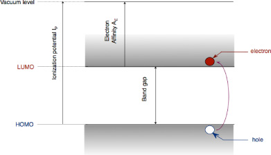
As already mentioned, organic semiconductors are generally listed in two categories according to their molecular structure: polymers and organic materials with low molar mass (less than 1,000 g/mol). These materials are conjugated systems made up of the alternation of single and double carbon-carbon bonds. These double bonds associate a single bond σ, corresponding to the axial covering of hybrid orbitals sp2, with a bond π coming from the lateral covering of two nonhybrid atomic orbitals pz. The molecular orbitals can be bonding (σ, π) or antibinding (σ*, π*) depending on whether the linear combination of atomic orbitals corresponds to an addition or a subtraction of associated wave functions. The difference of energy between the Highest Occupied Molecular Orbital (HOMO), and the lowest unoccupied Molecular Orbital (LUMO) corresponds to the distance between bonding π and antibonding π* orbitals; it makes up the forbidden energy band also called the “band gap”. Although the terms HOMO and LUMO characterize insulated molecules, it is customary to use them to describe solids. We shall therefore consider that the position of the HOMO with respect to the vacuum level corresponds with a solid to the ionization potential IP. Similarly, the position of the LUMO with respect to the vacuum level corresponds to the electron affinity AE of the solid (Figure 20.1).
In organic semiconductors, the transport of charge carriers (electrons or holes) is predominantly ensured by hops between molecular sites or between different polymer chains. In strongly ordered molecular materials, such as pentacene crystals, carriers evolve between nearby molecules permitting mobilities of the order of 35 cm2/V.s to be reached at ambient temperature [JUR 04]. However, in the most disordered molecular systems and polymers, mobilities only reach 10−3 to 10−5 times this upper value [MOZ 05, CHE 00]. By comparison, they can reach μ e = 1,500 cm2/V.s for electrons and μt = 450cm2/V.s for holes in monocrystalline silicon. The charge transport can be improved by the conditions of preparation of thin organic layers: deposition methods, purity of materials. Weak mobility values consequently give rise to a weak conductivity of the order of 10−6 S.cm−1 in organic semiconductors. However, these materials are only rarely doped, unlike their inorganic counterparts. The electron donor or acceptor character of the material is here an intrinsic property defined with respect to the electronegativity scale of the material considered. The more electronegative it is, the more its acceptor character is emphasized because it has more power to attract electrons. The material is generally called an acceptor if it possesses a large electron affinity value (of the order of 4 eV); it is considered a donor if the value of its ionization energy is weak (typically 5 eV).
20.3. Electrical and optical characteristics of organic semiconductors
The choice criteria of organic materials used in the manufacture of electroluminescent diodes and photovoltaic cells must take into account the physico-chemical parameters required for the good working order of the component. A knowledge of the electrical and optical properties of organic semiconductors therefore plays a dominating role in the understanding of the functioning and the improvement performances of these devices. Numerous measurement techniques, intrinsic or not to organic semiconductors, were implemented to characterize them. This section will only mention the most common analysis methods permitting access to the energy levels of the materials, the mobility of charges and the properties of excitons created in films.
The position of the HOMO and LUMO electronic levels of an organic material closely depend on its physical and chemical characteristics, but also on its environment. The technique chosen to determine them can perturb the measurement and distort the results. The most common experimental method to determine these values is cyclic voltammetry. This method relies on determination by electrochemistry of oxidation and reduction potentials of the material which we wish to study. It permits the characterization of thin films deposited on one of the electrodes used for measurement (a working electrode) or solution molecules in the electrolyte. Ultraviolet Photoelectron Spectroscopy (or UPS) permits a much more rigorous measurement of the ionization potential of organic semiconductors. It is made on thin films (a few hundred angströms for the thickest) placed in an ultrahigh vacuum chamber and requires an intense luminous and monochromatic source, and an electron analysis system. The absorption by an insulated molecule of a UV photon of sufficient energy h? causes the emission of an electron with kinetic energy EK. UPS measures the quantity of electrons emitted with a given energy. The variation of the scanning voltage applied to the sample permits a spectrum to be obtained which traces the exact match between the kinetic energy distribution of these electrons and the energetic states of the molecule. This characterization technique, applied during the growing of a thin film, permits access to information concerning the following points:
– the shift of the valence bands, which corresponds to a variation of the HOMO level position during the passage from one material to another;
– the band bending caused by charge transfer corresponding to the difference in work function values of both materials put in contact [SCH 99];
– the possible formation of a dipole at the interface [HIL 002].
The shift of the LUMO level is only accessible by spectroscopy measurement of inverse photoelectron (IPES) made in the same conditions [HIL 00_1].
The Time of Flight (or TOF) is amongst the most used techniques to determine the mobility of charge carriers in a solid semiconductor. The principle of this method lies in the measurement of time τtr taken by the electrons or the holes to traverse the sample which we wish to study. Electric charges are emitted by absorption of light generated by an impulsion laser. They are led by the electric field applied to the sample. The measurement of the charge mobility can also be made by making a Field Effect Transistor (or FET) whose active thin layer is composed of the studied material [HOR 98]. We deduce the mobility value of the current-voltage curves. We must note that the value obtained by this calculation depends on characteristics of the structure, such as contact resistance. The PR-TRMC method (Pulse-Radiolysis Time-Resolved Microwave Conductivity) is based on the examination of a material sample under the irradiation by a high frequency electron beam (20 MHz). This fairly complex measurement process does not permit the mobility of holes to be distinguished from that of electrons, and constitutes a microscopic analysis of the charge’s mobility [CRA 96].
All these electrical characterizations are most often completed by optical measurements (photoluminescence, UV-visible absorption, etc.) which, associated with mathematical models, allow information such as the binding energy of excitons and their diffusion length in a given material to be accessed. Finally, we should mention electro-absorption spectroscopy which, applied to a functioning multilayer component, supplies information on the internal electric field distribution.
20.4. Application to electroluminescent devices
20.4.1. General structure of an organic electroluminescent diode (OLED)
The basic structure of an organic electroluminescent diode is a monolayer structure in which a luminescent material is taken “in sandwich” between two electrodes, one of which must be transparent to permit the passage of photons. The use of appropriate electrode materials allows the injection of electrons and holes, which leads to the formation of excitons and their radiative recombination in the organic layer. When this structure was applied to organic crystals, the studies showed that the recombination zone was localized near one of the electrodes owing to the different injection and transport properties of electrons and holes [KAL 94]. The monolayer structures lead to weak electroluminescence efficiencies, on the one hand because the concentrations of electrons and holes are not balanced, and on the other hand because the defects near the electrodes are non-radiative recombination sources [CHO 97].
In multilayer structures, the injection and the transport of electrons and holes are attributed to distinct layers; moreover, the recombinations are localized at the level of an organic heterojunction owing to a confinement of charges. In the example of Figure 20.2, a bilayer diode consists of a material preferentially transporting holes (a Hole-Transporting Layer, or HTL) and an Electron-Transporting Layer (ETL) Emitter of Light (EML). When the diode is in direct polarization, the electrons and holes penetrate, respectively, the LUMO level of the ETL layer and the HOMO level of the HTL layer by passing or traversing energy barriers of different heights. The charge carriers are then partially blocked at the interface between both organic materials because of the difference in their HOMO and LUMO energy levels. The formation and the recombination of excitons are therefore produced at the level of this interface. We note that the representation below is very schematic. Indeed, the rigidity of energy bands supposes the absence of charges within organic layers and therefore do not correspond to the reality. Furthermore, if it is established that an effective injection of charges at the anode and the cathode, respectively, require a metal of high and low work function, the characteristics intrinsic to the materials are not enough to precisely describe the electronic structure at the interfaces. In particular, the physico-chemical interaction between the materials [NGU 01] and the space charge [TUT 03] present in the layers are likely to modify the injection and transport conditions.

20.4.2. Electroluminescence efficiency
A simplified description of the functioning of OLEDs allowss the different components of the electroluminescence efficiency to be revealed.
First, the exciton formation results from the injection and transport of electrons and holes from electrodes, and the excitation of luminescent molecules. The efficiency of this process is therefore related to the equilibrium of both currents and to the absence of defects, which would lead to non-radiative de-excitations. It can be characterized by:
where Jexc is the current density leading to the formation of excitons and Jtot is the total current density.
The formation of excitons can give rise to singlet or triplet excited states which are distinguished by their spin value (S = 0 or S = 1). The singlet states, which lead to fluorescence, statistically constitute 25% of the excited states. This value was experimentally confirmed in low molar mass materials, while the rates of singlet excitons greater than 50% were revealed in certain electroluminescent polymers. The phosphorescence, corresponding to a radiative de-excitation from the triplet states, is most often invisible at ambient temperature because it is associated with a forbidden transition. Although certain compounds are phosphorescent at ambient temperature and lead to a maximum theoretical efficiency of 100% [HOL 05], the fluorescence therefore leads, for “small molecules”, to:
The de-excitation from the excited singlet states can be produced in a radiative or non-radiative manner. The rate of radiative de-excitations is defined by the photoluminescence (generally fluorescence) efficiency ηPL of the emitting material. We note that if the fluorescence efficiencies of the order of 80% are commonly obtained in solution, the measured values for thin layers [GAR 96] are clearly reduced because of the interaction between molecules.
The last process which limits electroluminescence efficiency is the reabsorption of the light by the adjacent organic layers, and its confinement due to organic layers and the use of a glass substrate. This latter phenomenon is particularly important because we estimate that the fraction of light ηopt which comes out at the surface of the component is generally only of the order of 20% [GU 97].
From the above reasoning, we deduce the expression of the external quantum efficiency of electroluminescence, a ratio between the number of injected charges and the number of emitted photons:
The luminous efficiency (in lm/W) is frequently used to characterize the components. It expresses, in photometric units [SUR 00], their power efficiency:
where hv is the energy of the emitted photons and qV is the energy of the electrons submitted to the polarization voltage of the diode V.
20.4.3. Advancement of the technology
The craze created by organic electroluminescence since the late eighties allowed the understanding of its fundamental mechanisms, the development of numerous luminescent materials [MIT 00] and the development of suitable technologies (see section 20.6). Whereas the lifetime [SAT 98] of the components initially seemed to constitute a serious slowdown for their commercialization, passive matrix organic displays are today present in numerous commercial objects (cameras, telephones, etc.). Nevertheless, the interest aroused by OLEDs concerns, above all, visualization and, more recently, lighting.
Organic electroluminescence presents numerous advantages towards current visualization technologies. Indeed, it allows us to make very thin light devices; unlike liquid crystal screens, electroluminescent screens do not require any backlighting and do not present any restriction in viewing angle. As we shall see later, the processing techniques of electroluminescent materials are relatively simple. Finally, the realization of components on flexible substrates is conceivable. Numerous prototypes of organic screens have been presented, the largest with a forty inch-diagonal and a definition of 12,805,800 pixels (WXGA mode). However, the commercialization of organic screens has been slowed down by the difficulty of making large active matrices fitted to the electronic addressing of OLEDs at a reasonable cost, and for the stability problems of matrix luminescent materials.
The emission of white light by electroluminescent organic diodes (WOLEDs) can be obtained by the addition of two or three colors emitted from one [YAN 00] or several layer(s). The first advantage of these components is that their emission spectrum can be modulated on demand by modifying, for given materials, the thickness of different layers [JOL 98] or their concentration. Moreover, the possibility of making luminous surfaces extended on rigid or flexible substrates brings new perspectives in the lightning field. Finally, the interest in OLEDs appeared following a constant increase in their luminous efficiency. Owing to the recent use of phosphorescent materials, the values reached are today of the order of those measured in incandescent lamps (from 13 to 20 lm/W). Nevertheless, this technology must still be developed to be able to envisage the commercialization of electroluminescent lightning panels.
20.5. Application to photovoltaic conversion
20.5.1. General structure of an organic photovoltaic cell
The structure of an organic photovoltaic cell is perfectly similar to that of an OLED. We must, however, distinguish two types of structures: the bilayer structure composed of a heterojunction between a donor material and an acceptor material, and the volume heterojunction commonly called a “blend” structure. This latter category of cells consists of a mixture in volume donor and acceptor materials. The donor is most often a polymer associated with a fullerene C60 derivative, which plays the role of acceptor. This molecule is generally functionalized in order to present a better solubility in the matrix polymer. A rigorous control of the mixture’s morphology permits an interpenetrated lattice in both materials to be obtained, which increases the dissociation rates of the created excitons. Promising efficiencies of conversion (3.1%) have thus been reached [AER 02], but the main problem still remains the transport of charges towards the electrodes. The realization of intermediate structures, where a donor–acceptor mixture is inserted between donor and acceptor layers, will help circumvent this difficulty [PEU 03].
20.5.2. Functioning of an organic photovoltaic cell
The functioning of such components can be described as being the inverse of that of an OLED. The different stages of organic photovoltaic conversion are detailed below.
The first stage is the absorption of photons in the organic film. It is expressed by the energy supply to the HOMO level electrons. The transition towards the LUMO level leads to the outbreak of a hole which remains connected to the electron by mutual electrostatic interaction. The electrically neutral electron-hole couple is then called an exciton. In inorganic materials, the binding energy of these excitons is very weak (14.7 meV for silicon) and the thermal energy is sufficient, at ambient temperature, to separate both connected charges. It is different in organic materials since the binding energy most often reaches values of the order of 0.2 eV. The result is a difficulty to dissociate the charge carriers which remain connected at ambient temperature.
The second stage is the diffusion of excitons over a distance, LD, depending on the material. The separation of charges is possible if the excitons rejoin the donor-acceptor junction where the electric field is sufficiently strong.
The dissociation of the excitons which reach the interface between both organic materials represents the third stage of the process. The electrons are attracted to the material having a high electron affinity and the holes by the material having a weak ionization potential. If the dissociation is made far from the interface in a neutral region, the electron and the hole end up recombining.
Finally, the charge carriers thus created rejoin the electrodes and the circuit outside the cell. The transport of charges towards the electrodes is controlled by the mobilities of carriers in the organic layers.
The characteristic parameters of a photovoltaic cell are deduced from the recording of the current-voltage curve under illumination. The most significative parameter is the fill factor, FF, which accounts for the quality of the form of curves. It is determined from the following expression:
where Icc is the short circuit current, Vco the open circuit voltage, and Im and Vm represent the current and the voltage of the functioning point which allows the maximum power (Pm) of the cell to be extracted.
The EQE (External Quantum Efficiency) is defined by the ratio of the number of electrons flowing in the external circuit connected to the cell to the number of incident photons. The EQE is deduced from the spectral response of the solar cell SR(λ):
where φ(λ) (W/m2) represents the luminous intensity by illuminated unit surface, Jcc(λ) (W/m2) the density of short circuit current for a given wavelength λ.
The efficiency of power conversion, η, is defined by the ratio of the maximal power delivered by the cell to the incident luminous power Pin:
The maximal conversion efficiency of a cell is only significant for a spectral distribution and a given intensity. The most commonly used standard irradiation corresponds to a mass air number AM 1.5 [PRO 97].
20.5.3. Advancement of the technology
The synthesis of new molecules better fitted to photovoltaic cells and the outbreak of new architectures of devices led to the acceleration of the development of this type of structure. During the last 20 years, the main efforts concerning the manufacture of cells have been concentrated on the addition of new layers at the interface level between the electrodes and organic films. Thus, the insertion between the ITO and the donor of a poly(3,4-ethylene dioxithiophene) (PEDOT) doped with poly(styrene sulphonate) (PSS) layer allows, in certain cases, an improvement of the conversion efficiency of cells to be achieved. As for the cathode, the deposition of lithium fluoride (LiF) and/or bathocuproine (BCP) allows the acceptor material to be protected during the deposition of the metal which often causes malfunctions of the component. The role of the BCP also consists of confining excitons to avoid them coming and recombining at the cathode/acceptor interface, and thus improving the conversion efficiency of the cell [PEU 00]. The realization of piled up cells (or tandem cells) allowing the domain of absorption of the component to be widened, led to conversion efficiencies of 5% [XUE 04]. One of the parameters restricting the performances of organic photovoltaic cells is the weak mobility of charges in the materials. One of the conceived solutions for an increase in this mobility is to make anisotropic films from ordered molecules. Mobilities of the order of 10−1 cm2/V.s could thus be measured in columnar phases of discotic liquid crystals [ADA 94]. A few cells were produced from these materials; however, the organization of molecules remains an important challenge.
The improvement of performance of the cells composed of mixed donor-acceptor materials is strongly related to the solubility and morphology of the films. These parameters strongly depend on the chosen solvent, which can cause strong variations on the characteristics of cells. Thus, for ITO/PEDOT/MDMO-PPV:PCBM/LiF/Al type cells, the conversion efficiency increases from 0.9% to 2.5% by replacing chlorobenzene with toluene [SHA 01]. One of the routes explored to avoid the formation of aggregates during deposition is to chemically connect the donor and acceptor molecules. The weak conductivity of these components limits the efficiency of this type of cell [NIE 04]. One of the main weaknesses of these cells, however, remains the stability issue already encountered in the OLEDs [KRO 02]. It is related to the nature of molecules, sensitive to oxygen and water vapor, but also to chemical reactions which can be produced at the interface between the electrodes and organic films. It is therefore of prime importance to protect the components by a layer impermeable to oxygen and water vapor during their functioning.
Over the last five years, progress in the synthesis and finalization of organic photovoltaic materials have allowed an increase in conversion efficiency from 1 to 5%, whether for bilayer heterojunctions or in volume. However, important research efforts still need to be pursued in the improvement and understanding of the functioning of these devices in order to conceive their commercialization.
20.6. The processing of organic semiconductors
We present below the main techniques which have been proposed to process organic semiconductors. Generally, polymers are deposited in the form of a solution whereas “small molecules” are vacuum evaporated. Certain techniques only allow surfaces to be uniformly covered, whilst others, more promising, allow the formation of patterns such as pixels.
20.6.1. Deposition of polymer solutions
20.6.1.1. Deposition by spreading
The deposition of polymers by centrifugation, or “spin coating”, is commonly used in microelectronics to deposit photosensitive resins. A film is obtained by spreading a polymer solution and simultaneously evaporating the solvent. Its thickness is then mainly determined by the rotation speed of the spin-coater and by the concentration, and therefore the viscosity, of the solution [FLA 84]. Although simple to implement, this technique does not permit large surfaces to be covered, does not guarantee a uniformity of the thickness and leads to large material losses. Alternative techniques such as pulverizing or spreading with the aid of a metallic strip [JOL 04] have been developed for diverse applications, but they are not very suitable for the realization of layers with a thickness smaller than a micrometer.
20.6.1.2. “Inkjet” deposition
“Inkjet” deposition technology [CAL 01, SHI 03] turns out to be very promising for the realization of organic components: not only does it allow the formation of polymer patterns, by it could also be applied to low molar mass dendrimers. The principle of this method consists of ejecting drops of a solution of a polymer from a micrometer sized nozzle. The red, green and blue (RGB) pixels of a screen are thus obtained by leaving drops between the polymer walls preformed on the substrate, and by realizing three successive passages. Although stemming from a very widespread printing technique, we must note that its application to organic semiconductors is not immediate. Indeed, the additives used in inks to optimize their viscosity, their surface tension and their drying speed, cannot be applied to organic semiconductors which must be pure. Furthermore, their choice lies more on their electro-optical properties and stability than on their mechanical properties.
20.6.2. Vapor phase deposition of low molar mass materials
20.6.2.1. Deposition by thermal evaporation under secondary vacuum
Vacuum thermal evaporation (or sublimation) [HOL 70] is suitable for the deposition of “small molecules” providing that they are not subjected to a thermal degradation during the operation. The materials to be evaporated are arranged in a crucible and heated by Joule effect under a secondary vacuum (∼ 10−4 Pa); a deposition is then produced on the samples placed above, in conditions (speed, thickness) controlled in situ by means of a vibrating quartz microbalance. The main advantage of this technique is that it guarantees a high purity of layers, more difficult to obtain in the case of polymers. The introduction of dopants is nevertheless possible by co-evaporation of both materials. Also applied to metals, vacuum evaporation permits the manufacture of components in a unique device. The main disadvantages of this technique are the difficulty to make deposits of uniform thickness on an extended surface and the important material losses it generates.
20.6.2.2. Low-pressure vapor phase deposition
Low-pressure vapor phase deposition [BAL 98, SHT 01] solves the problems inherent to vacuum evaporation. This method consists of evaporating the materials, and transporting them towards a distinct deposition chamber by means of a heated inert gas. The deposition speed is then controlled by the gas flux, the pressure of the enclosure (of the order of 10−1 to 102 Pa) and the temperature of the source and the substrate. Unlike vacuum evaporation, the organic flux can be uniformly spread on any surface by a “shower-head” at a few centimeters’ distance; this also allows material losses to be minimized.
An analogous “inkjet” printing method is developed in the case of vapor phase deposition [SHT 04]. It consists of sending the organic vapor jet on the cooled substrate by a nozzle situated at very short distance (∼10–100 μm). It then becomes possible to form patterns from “small molecules”.
20.6.3. Laser thermal transfer of organic materials
Laser thermal transfer of organic materials [ELI 03, SUH 03] on a substrate was initially developed for the realization of RGB filters, used in liquid crystal screens. This method consists of transferring a polymer or a material of low molar mass from a “donor” substrate towards an “acceptor” substrate by laser ablation.
The donor substrate is composed of a photosensitive layer which converts luminous energy into thermal energy; it is covered with the organic material(s) to be transferred. This is done by assembling both substrates and by selectively irradiating certain zones with the aid of an infrared laser beam.
The advantages of this technique are its high precision (of the order of 2.5 μm), the possibility of applying it to extended surfaces and the absence of solvents. It could be applied not only to the realization of organic pixel matrices but also to the preparation of substrates (for the deposition of polymer barriers) for matrices manufactured by “inkjet”.
20.7. Conclusion
This chapter has successively tackled the history of organic semiconductors, their electronic properties and the main characterization methods used to describe them. We have then presented two essential applications, electroluminescent diodes and organic photovoltaic cells, before listing the deposition methods proposed for their manufacture. We should stress that the simplicity of processing organic semiconductors is a strong point in favor of these materials. Organic electronics give rise to a lot of interest because of the new applications they shed light on (flexible luminous or photovoltaic surfaces, “roll-to-roll” production by printing techniques, etc.).
We have also seen that organic semiconductors are distinguished from their inorganic counterparts, particularly from the viewpoint of charge mobility values. The revelation of well-known problems in the field of dielectric materials (injection and transport phenomena, space charge effects, etc.) justifies the integration of this chapter in a book on dielectric materials.
20.8. Bibliography
[ADA 94] ADAM D., SHUHMACHER P., SIMMERER J., HÄUSSLING L., SIEMENSMEYER K. ETZBACH K.H., RINGSDORF H., HAARER D., “Fast photoconduction in the highly ordered columnar phase of a discotic liquid crystal”, Nature, vol. 371, no. 6493, p. 141–143, 1994.
[AER 02] AERNOUTS T., GEENS W., POORTMANS J., HEREMANS P., BORGHS S., MERTENS R., “Extraction of bulk and contact components of the series resistance in organic bulk donnor–acceptor heterojunctions”, Thin Solid Films, vol. 403–404, p. 297–301, 2002.
[BAL 98] BALDO M., DEUTSCH M., BURROWS P., GOSSENBERGER H., GERSTENBERG M., BAN V., FORREST S., “Organic vapor phase deposition”, Adv. Mater., vol. 10, no. 18 p. 1505–1514, 1998.
[BUR 90] BURROUGHES J.H., BRADLEY D.D.C., BROWN A.R., MARKS R.N., MACKAY K., FRIEND R.H., BURNS P.L., HOLMES A.B., “Light-emitting diodes based on conjugated polymers”, Nature, vol. 347, no. 6293, p. 539–541, 1990.
[CAL 01] CALVERT P., “Inkjet printing for materials and devices”, Chem. Mater., vol. 13, no. 10, p. 3299–3305, 2001.
[CHE 00] CHEN B., LEE C., LEE S., WEBB P., CHAN Y., GAMBLING W., TIAN H., ZHU W., “Improved time-of-flight technique for measuring carrier mobility in thin films of organic electroluminescent materials”, Jpn. J. Appl. Phys., vol. 39, p. 1190–1192, 2000.
[CHO 97] CHOONG V.E., PARK Y., SHIVAPARAN N., TANG C.W., GAO Y., “Deposition-induced photoluminescence quenching of tris-(8-hydroxyquinoline) aluminum”, Appl. Phys. Lett., vol. 71, no. 8, p. 1005–1007, 1997.
[CRA 96] VAN DE CRAATS A.M., WARMAN J.M., DE HAAS M.P., ADAM D., SIMMERER J., HAARER D., SCHUHMACHER P., “The mobility of charge carrier in all four phases of the columnar discotic material hexakis(hexylthio)triphenylene: combined TOF and PR-TRMC results”, Adv. Mater., vol. 8, no. 10, p. 823–826, 1996.
[ELI 03] ELIZURAND E., GELBART D., “Printing methods for flat-panel display manufacturing”, J. Graphic Technol., vol. 1, p. 1–5, 2003.
[FLA 84] FLACK W.W., SOONG D.S., BELL A.T., HESS D.W., “A mathematical model for spin coating of polymer resists”, J. Appl. Phys., vol. 56, no. 4, p. 1199–1206, 1984.
[GAR 96] GARBUZOV D.Z., BULOVIC V., BURROWS P.E., FORREST S.R., “Photoluminescence efficiency and absorption of aluminum-tris-quinolate (Alq3) thin films”, Chem. Phys. Lett., vol. 249, nos 5–6, p. 433–437, 1996.
[GU 97] GU G., GARBUZOV D.Z., BURROWS P.E., VENKATESH S., FORREST S.R., “High-external-quantum-efficiency organic light-emitting devices”, Opt. Lett., vol. 22, no. 6, p. 396–398, 1997.
[HIL 00_1] HILL I.G., KHAN A., SOOS Z.G., PASCAL R.A. Jr., “Charge-separation energy in films of π-conjugated molecules”, Chem. Phys. Lett., vol. 327, nos 3–4, p. 181–188, 2000.
[HIL 00_2] HILL I.G., MILLIRON D., SCHWARTZ J., KHAN A., “Organic semiconductor interfaces: electronic structure and transport properties”, Appl. Surf. Sci., vol. 166, nos 1– 4, p. 354–362, 2000.
[HOL 70] HOLLAND L., Vacuum deposition of thin films, Chapman & Hall, London, 1970.
[HOL 05] HOLDER E., LANGEVELD B.M.W., SCHUBERT U.S., “New trends in the use of transition metal-ligand complexes for applications in electroluminescent devices”, Adv. Mater., vol. 17, no. 9, p. 1109–1121, 2005.
[HOR 98] HOROWITZ G., “Organic field-effect transistors”, Adv. Mater., vol. 10, no. 5, p. 365– 377, 1998.
[JOL 98] JOLINAT P., CLERGEREAUX R., FARENC J., DESTRUEL P., “The effect of the thicknesses of the various layers on the color emitted by an organic electroluminescent device”, J. Phys. D: Appl. Phys., vol. 31, no. 10, p. 1257–1262, 1998.
[JOL 04] JOLINAT P., “Dépôts de polymères”, Traité EGEM-Techniques de fabrication des microsystèmes, Hermès Science Publications, vol. 1, p. 121–142, 2004.
[JUR 04] JURCHESCU O.D., BAAS J., PALSTRA T.T.M., “Effect of impurities on the mobility of single cristal pentacene”, Appl. Phys. Lett., vol. 84, no. 16, p. 3061–3063, 2004.
[KAL 94] KALINOWSKI J., “Space-resolved recombination electroluminescence in organic crystals”, Synth. Met., vol. 64, nos 2–3, p. 123–132, 1994.
[KRO 02] KROON J.M., WIENK M.M., VERHEES W.J.H., HUMMELEN J.C., “Accurate efficiency determination and stability studies of conjugated polymer/fullerene solar cells”, Thin Solid Films, vol. 403–404, p. 223–228, 2002.
[LAW 93] LAW K.Y., “Organic photoconductive materials: recent trends and developments”, Chem. Rev., vol. 93, no. 1, p. 449–486, 1993.
[LOU 88] LOUTFY R.O., HOR A.M., HSIAO C.K., BARANYI G., KAZMAIER P., “Organic photoconductive materials”, Pure Appl. Chem., vol. 60, no. 7, p. 1047–1054, 1988.
[MIT 00] MITSCHKE U., BÄUERLE P., “The electroluminescence of organic materials”, J. Mater. Chem., vol. 10, no. 7, p. 1471–1507, 2000.
[MOZ 05] MOZER A.J., SARICIFTCI N.S, PIVRIKAS A. ÖSTERBACKA R., JUSKA G., BRASSAT L., BÄSSLER H., “Charge carrier mobility in regioregular poly(3-hexylthiophene) probed by transient conductivity techniques: A comparative study”, Phys. Rev. B, vol. 71, no. 3, p. 035214_1-035214_9, 2005.
[NGU 01] NGUYEN T.P., IP J., JOLINAT P., DESTRUEL P., “XPS and sputtering study of the Alq3/electrode interfaces in organic light emitting diodes”, Appl. Surf. Sci., vol. 172, nos 1–2, p. 75–83, 2001.
[NIE 04] NIERENGARTEN J.F., “Fullerene-(p-conjugated oligomer) dyads as active photovoltaic materials”, Sol. Energy Mater. Sol. Cells, vol. 83, nos 2–3, p. 187–199, 2004.
[PEU 00] PEUMANS P., BULOVIC V., FORREST S.R., “Efficient photon harvesting at high optical intensities in ultrathin organic double-heterostructure photovoltaïc diodes”, Appl. Phys. Lett., vol. 76, p. 2650–2652, 2000.
[PEU 03] PEUMANS P., UCHIDA S., FORREST S.R., “Efficient bulk heterojunction photovoltaic cells using small molecular weight organic thin films”, Nature, vol. 425, no. 6945, p. 158–162, 2003.
[POP 63] POPE M., KALLMANN H.P., MAGNANTE P., “Electroluminescence in organic crystals”, J. Chem. Phys., vol. 38, no. 9, p. 2042–2043, avril 1963.
[PRO 97] PROTIN L., ASTIER S., “Convertisseurs photovoltaïques”, Techniques de l’ingénieur, D3360, 08–1997.
[SAT 98] SATO Y., ICHINOSAWA S., KANAI H., “Operation characteristics and degradation of organic electroluminescent devices”, IEEE J. Select. Top. Quant. Electron., vol. 4, no. 1, p. 40–48, 1998.
[SCH 99] SCHLAF R., SCHROEDER P.G., NELSON M.W., PARKINSON B.A., LEE P.A., NEBESNY K.W., ARMSTRONG N.R., “Observation of strong band bending in perylene tetracarboxylic dianhydride thin films grown on SnS2”, J. Appl. Phys., vol. 86, no. 3, p. 1499–1509, 1999.
[SHA 01] SHAHEEN S.E., BRABEC C.J., SARICIFTCI N.S., PADINGER F., FROMHERZ T., HUMMELEN J.C. “2.5% efficient organic plastic solar cells”, Appl. Phys. Lett., vol. 78, no. 6, p. 841–843, 2001.
[SHI 01] SHIRAKAWA H., “The discovery of polyacetylene film: the dawning of an era of conducting polymers (Nobel lecture)”, Angew. Chem. Int. Ed., vol. 40, no. 14, p. 2574–2580, 2001.
[SHI 03] SHIMODA T., MORII K., SEKI S., KIGUCHI H., “Inkjet printing of light-emitting polymer displays”, Mater. Res. Soc. Bull., vol. 28, no. 11, p. 821–827, 2003.
[SHT 01] SHTEIN M., GOSSENBERGER H.F., BENZIGER J.B., FORREST S.R., “Material transport regimes and mechanisms for growth of molecular organic thin films using low-pressure organic vapor phase deposition”, J. Appl. Phys., vol. 89, p. 1470–1476, 2001.
[SHT 04] SHTEIN M., PEUMANS P., BENZIGER J.B., FORREST S.R. “Direct, mask- and solvent-free printing of molecular organic semiconductors”, Adv. Mater., vol. 16, no. 2, no. 18, p. 1615–1620, 2004.
[SUH 03] SUH M.C., CHIN B.D., KIM M.H., KANG T.M., LEE S.T., “Enhanced luminance of blue light-emitting polymers by blending with hole-transporting materials”, Adv. Mater., vol. 15, no. 15, p. 1254–1258, 2003.
[SUR 00] SURREL J., “Radiométrie – Photométrie”, Optique et photonique, vol. 1, p. 51– 54, 2000.
[TAN 87] TANG C.W., VANSLYKE S.A., “Organic electroluminescent diodes”, Appl. Phys. Lett., vol. 51, no. 12, p. 913–915, 1987.
[TUT 03] TUTIS E., BERNER D., ZUPPIROLI L., “Internal electric field and charge distribution in multilayer organic light-emitting diodes”, J. Appl. Phys., vol. 93, no. 8, p. 4594–4602, 2003.
[YAN 00] YANG J.P., JIN Y.D., HEREMANS P.L., HOEFNAGELS R., DIELTIENS P., BLOCKHUYS F., GEISE H.J., VAN DER AUWERAER M., BORGHS G., “White light emission from a single layer organic light emitting diode fabricated by spincoating”, Chem. Phys. Lett., vol. 325, nos 1–3, p. 251–256, 2000.
[XUE 04] XUE J., UCHIDA S., RAND B.P., FORREST S.R., “Assymetric tandem organic photovoltaic cells with hybrid planar-mixed molecular heterojunctions”, Appl. Phys. Lett., vol. 85, no. 23, p. 5757–5759, 2004.
1 Chapter written by Pascale JOLINAT and Isabelle SEGUY.