
Chapter 7
Optimal Power Components Selection
Having understood the basic concepts behind stress derating and reliability in the preceding chapter, this one focuses on the accurate computation of the actual voltage and current stresses occurring inside a power converter. A lookup reference chart with the voltage stresses on all the power components in all major topologies is presented. Topologies include the half-bridge, full-bridge, push–pull, 2-switch forward, Cuk, Sepic, Zeta, and the active forward clamp. Then, attention turns toward calculating the peak, average, and RMS currents of the key topologies, including both DC–DC and AC–DC converters. Detailed derivations with simplifying formulas for general RMS calculations are included. Finally, the correct estimation of worst-case current stresses as the input voltage varies, is tackled. “Stress Spider” diagrams are presented for the three fundamental topologies, so as to easily visualize how a given stress varies with line voltage, and thereby correctly pick a component for a given application.
Overview
In Chapter 6, we reviewed basic reliability and stress derating principles with emphasis on understanding datasheets and power component ratings. Our focus was on the strength aspect of the “matchmaking” process as we called it. In this chapter we turn our attention to the stresses aspect of that process. We thus hope to create viable and reliable component choices.
When designing and evaluating wide-input converters, we need to clearly identify the specific input voltage point at which a given stress reaches its maximum. Thereby we can deduce the worst-case operating stresses in the converter over its entire range of operation. That analysis will lead us to what we call the “Stress Spider” later in this chapter.
We can ask: is component selection only about matching strength (of a part) to (the applied) stress? No. That may in fact turn out to be only a pre-requisite. In Chapter 13, we will see how, for example, the input and output ripple requirements can eventually dictate the choice of the power components. In Chapter 9, we will discuss hysteretic Buck regulators for example, which depend on sufficient output voltage ripple to operate satisfactorily. In other words, various factors can affect final component choices. This chapter will help us at least shortlist eligible candidates.
The Key Stresses in Power Converters
Voltage stress is not only the most important, but also relatively the simplest to calculate and tackle. We know that if the voltage on a power semiconductor even momentarily exceeds its published Absolute Maximum (Abs Max) rating, it will very likely be destroyed almost immediately. In comparison, the current rating is usually not of such immediate concern, since it is typically (not always) thermal in nature, and is therefore comparatively slower-acting. In general, we can often inadvertently, or even sometimes with judicious deliberation, exceed the current ratings of a semiconductor somewhat, then “back off” quickly, without much impact. But note that this “forgiveness factor” should not be taken for granted. For example, if core saturation starts to occur, destruction can be almost immediate as shown in Figure 2.7.
We will now summarize our key concerns.
(A) Voltage stresses inside a converter are invariably at their highest when the input voltage is raised to its maximum value (VINMAX). We may need to carefully decipher what specific load conditions correspond to the highest voltage stresses, and what those stresses are. For example, in a flyback, the leakage inductance voltage spike will be worse at high loads — the spike will be higher despite the zener clamp (zener voltage depends on current), and also of longer duration (width of spike, i.e., its residual energy). In a Forward converter, the reverse voltage on the output diode may be the highest at light loads. And so on.
Summarizing: the primary voltage stress we need to worry about is
• VPK, the peak voltage (on any component), since that represents the maximum instantaneous voltage. We know from Chapter 6 that too high a voltage can cause semiconductor junctions to (instantaneously) avalanche and/or snapback.
(B) Current stresses inside a converter are invariably at their highest when the load is raised to its maximum rated value (IO). We need to carefully decipher what specific input voltage conditions correspond to the highest current stresses, and exactly what those stresses are. These calculations can become very complicated.
Summarizing: the primary current stresses we need to worry about are
• IRMS, the root mean square (RMS) current, since that determines the conduction losses in MOSFETs (explained further below).
• IAVG, the average current, since that determines the conduction losses in diodes (explained further below).
• IPK, the peak current, since that can instantaneously cause core saturation and consequent destruction of the MOSFET. Remember that in any basic (inductor-based) DC–DC topology, the peak currents in the switch, diode, and inductor are all the same.
Waveforms and Peak Voltage Stresses for Different Topologies
We first look at voltage stresses. In Figures 7.1 and 7.2, we have started by plotting the waveforms at the switching nodes of the main conventional topologies (marked “A” or “B”). The switching node is crucial since it is a node that is a point common to both the switch and diode. Thereafter, we take the difference of the voltages on either side of the component under consideration (switch or diode), and thereby calculate the voltage across it. That difference voltage can be generally expressed by an equation of the form “Vx–Vy.” Note that looking at any specific plot in the two figures, as we move along the x-axis (time increasing), in effect, a new phase of operation starts if either of the two voltages on either side of the component (Vx or Vy, or both) change. So, for each distinct phase of operation we then need to re-evaluate the difference voltage “Vx–Vy’.” In this manner, we generate the full voltage waveform across the component over the entire switching cycle.
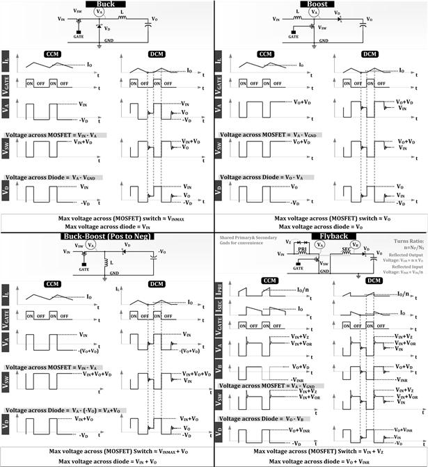
Figure 7.1: Voltage waveforms for the Buck, Boost, Buck-Boost, and Flyback.
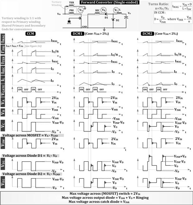
Figure 7.2: Voltage waveforms for the Single-Ended Forward Converter.
We can thus clearly identify the worst-case voltage stress across the component (diode or switch). Note that we have repeated the above-mentioned process for both “continuous conduction mode” (CCM) and “discontinuous conduction mode’ (DCM) (heavy and light loads), to ensure we are really discovering the worst-case voltage stress over the entire application conditions.
Note that we have not bothered to report any capacitor voltage stresses in the figures, because that is quite self-evident in all topologies. The simple rule is that the input capacitor must be rated for at least VINMAX, whereas the output capacitor should be rated for at least VO. There is nothing complicated there, though we may need to apply appropriate stress derating as discussed in Chapter 6.
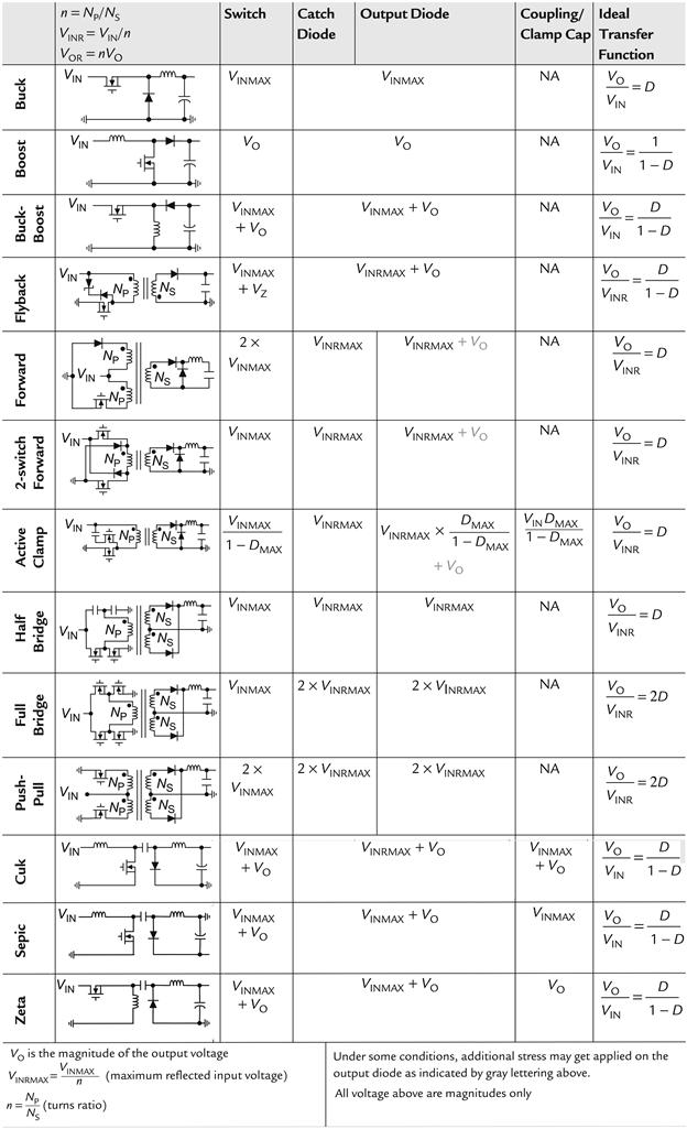
We have consolidated our findings for the diode and switch in an easy lookup chart: Table 7.1. Note that in this chart, there are several “new” topologies tabulated just for completeness sake. Many of these, but not all, are discussed in more detail in Chapter 9.
• We notice that on the extreme right-hand side of Figure 7.2 (the Forward converter figure), we have a special case of DCM where the inductor (output choke) reaches zero current and stays there (i.e., gets de-energized) before the transformer de-energizes. Admittedly, that situation can happen only under some rather unusual circumstances, like excessive transformer step-down ratios combined with light loads. But, if and when that happens, the voltage stress across the output diode D1 is not just VINR, as is usually stated in literature, but VINR+VO. The reason is the switching node on the secondary side (cathode of the diode) jumps up to VO since the output choke “dries up” (gets de-energized), while the anode of the diode is still being dragged low by the transformer winding — down to –VIN/n (i.e., –VINR), where n is the turns ratio NP/NS (n being much larger than 1 typically). That is the reason why we have written out the peak stresses as mentioned in Table 7.1 for the Forward converter.
• For an active clamp Forward converter, the high-stress situation for the output diode described above can happen much more readily, since the transformer is always in CCM, but the choke can go into DCM at light loads.
Note that for finding the peak voltage stresses, we are generally very interested in transient cases too. For example, we can hit DMAX under a sudden load/line change, even though we are operating at VINMAX, with a much lower steady-state duty cycle just prior to that sudden event. That explains the peak stresses reported in Table 7.1 for the active clamp Forward converter.
In an active clamp Forward converter, there is an additional MOSFET (clamp) as shown in Table 7.1. Functionally, it takes the place of the energy recovery diode in the conventional (single-ended) Forward converter. This topology and its voltage stress ratings, as presented in Table 7.1, are further discussed and derived in Chapter 9.
Note: The energy-recovery diode is in series with the tertiary (energy recovery) winding and its purpose is to ensure the transformer “resets” every cycle. In general, “reset” in any given magnetic component does not mean a return to zero current (or zero “net Ampere-turns” when talking about transformers) every cycle. As in the active clamp Forward converter transformer, reset just means the net Ampere-turns at the end of the switching cycle returns to exactly the same value it started the switching cycle off with. Intuitively, reset is simply a prerequisite for us to be able to label the magnetic component and thereby the converter as operating in a “steady (repetitive) state.”
Note: The tertiary winding diode can theoretically be placed either between the tertiary winding and the upper rail (as shown in Figure 7.2), or between the winding and ground as shown in Table 7.1. However, there is a preferred position as described in Chapter 9.
• The voltage ratings of any additional components of any Forward converter based topology mentioned above are the same as their corresponding switch voltage ratings. So, if in a universal input Forward converter, the main switch is rated >800 V, the energy recovery diode (or the active clamp switch) must be rated >800 V too.
• What if, instead of the single-ended Forward converter, we use a two-switch Forward converter (also called an “asymmetric half-bridge”)? This has two switches on either side of the Primary winding, driven in unison (in phase). There is no tertiary winding present to add any reflected voltage on top of the input voltage rail. Therefore, in this case, both the switches need to be rated only for VINMAX, not twice that as in the single-ended Forward. On the Secondary side, all the voltages are unchanged as compared to the single-ended Forward converter.
• Note that for a Buck-Boost, the diode and switch can see a maximum of VINMAX+VO, and must be rated accordingly (remember that we always use magnitudes of voltages in this book, and introduce signs only when necessary).
• The transformer-isolated version of the Buck-Boost, that is, the flyback, has an additional spike due to leakage inductance riding on top of the level VINMAX+VOR. The spike is limited by a zener of voltage VZ referenced to VIN rail. So, the maximum stress is VINMAX+VZ. See Figure 3.1 for more details.
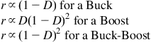
• As we will learn in Chapter 9, the Sepic, Cuk, and Zeta are composite topologies based on the Buck-Boost. The switch/diode voltage ratings are therefore exactly the same as for a Buck-Boost. The additional power component in these composite topologies is the coupling capacitor. The voltage on that can vary from one topology to another. It is VINMAX for Sepic, VO for Zeta, and VINMAX+VO for Cuk.
Table 7.1. Peak Voltage Stresses for Several Key Topologies.
|
In the next section, we start to look at the current stresses of the power components.
The Importance of RMS and Average Currents
Work (or energy) is done when charged particles (electrons) are transported across a potential barrier (voltage). We have the basic equation for energy as ε=V×Q, where Q is the amount of charge and V is the potential difference. Power (or dissipation) is, by definition, energy per second. So, we get ε/t≡P=V×Q/t=V×I. The last step follows because charge per second is, by definition, current. Therefore, we also get the definition of instantaneous dissipation as P(t) =V(t) ×I(t). This is a function of time, and can change from moment to moment. However, for a repetitive waveform, we can find its average value over one cycle. In steady state, that average value remains constant. By definition it is
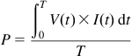
where T=1/fSW and fSW is the switching frequency.
This can be further simplified based on one of the following:
(a) V is constant:
Assuming V is a constant (as for a diode in forward conduction)
![]()
where ID_AVG is the average diode current.
(b) R is a constant:
Assuming an equivalent resistance (as for a MOSFET in full conduction)
![]()
so
![]()
where ISW_RMS is the RMS switch (in this case MOSFET) current.
That is why it is customary to calculate and use the average current to find the dissipation for a diode and the RMS current for the dissipation in a MOSFET.
Note that there is also a V×I (crossover loss) term occurring during every switching transition that we have neglected above in computing the dissipation. In effect, what we have calculated above is just conduction loss. Note that for a switch we always need to add a switching loss term to find the total dissipation (see Chapter 8). But in a diode (or synchronous FET), we usually consider its switching loss term as negligible. Note, however, that the catch diode’s characteristics (slow reverse recovery) might cause significantly higher crossover losses in the switch if not in the diode itself. On the other hand, Schottky diodes, though near-ideal diodes in that sense, can have significant reverse leakage dissipation term that we need to add to the total dissipation in the diode, as discussed in Chapter 6.
Similarly, for a capacitor, especially an electrolytic type, we need to ensure we do not exceed its published RMS (ripple) current rating, otherwise it will have a very short life indeed as also discussed in Chapter 6. We need to know its IRMS accurately.
At this juncture we need to gain some mastery over actually calculating RMS and average values for different topologies. We will also derive some of the key equations that appear in the Appendix of this book.
Note that several numerical examples based on this chapter, are provided in Chapter 19.
Calculation of RMS and Average Currents for Diode, FET, and Inductor
In Figure 7.3, we have provided the procedure for calculating the average/RMS currents of the switch, diode, and inductor, via “brute-force” integration techniques first. In general, we get
![]()
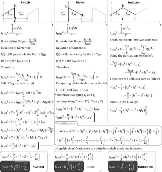
Figure 7.3: Integration method to derive RMS currents for MOSFET (Switch), diode, and inductor (any topology).
In Figure 7.4, we have provided an easy lookup formula that basically bypasses the above brute-force integration technique going forward. It provides the same results as above. The only restriction on using the simple method is that the waveform, however arbitrary, must be a combination of piecewise linear segments. The general rule to use is as per Figure 7.4
![]()
and
![]()
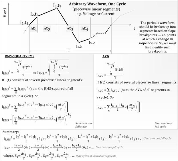
Figure 7.4: General equation to derive RMS/AVG for piecewise linear waveforms.
Applying the above techniques to the typical current waveforms of a power supply, we can also express the RMS in terms of the current ripple ratio r. This is shown in the embedded derivation in Figure 7.3. We thus get
![]()
where IL is the average inductor current (center of ramp). Keep in mind that as shown in Chapter 1, the center of ramp (IL above) varies for different topologies.
![]()
We thus get the equations for RMS currents (diode, switch, and inductor) as provided in the design table of the Appendix of this book.
Similarly, for average currents, the calculation is almost self-evident, but we can consult Figure 7.4 if in doubt. We get in general (calling D′ = 1–D)
![]()
This combined with the equations for IL for different topologies, as provided above, leads to the equations for average currents (diode, switch, and inductor) provided in the design table of the Appendix.
Calculation of RMS and Average Currents for Capacitors
Now we discuss a key rule that helps us calculate capacitor currents. First, it should be intuitively obvious that if we take a waveform, and, without changing its basic shape, translate it horizontally (sideways), its RMS and average values will be unchanged. That is equivalent to changing the “0” of the x-axis (time), and we did just that in Figure 7.3 while evaluating the RMS of the diode waveform. We realized that for repetitive events, nature (expressed as observed heat and heat-related effects in our case) cannot possibly depend on where we, as mere observers, choose to start counting time, that is, where we decide to put a stake in the ground labeled “t=0.” So, horizontal translation (“x-translation”) of a waveform cannot affect any results provided so far.
But what happens if we move the waveform vertically? Certainly, the RMS and average values will be affected. But we ask: is there any simplifying relationship, or rule, that we can identify under this “y-translation,” and perhaps exploit in future? There is one such rule. In Figure 7.5, we numerically validate a fundamental property of vertically translated waveforms (using the general RMS calculation method of Figure 7.4). It is
![]()
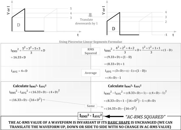
Figure 7.5: AC RMS of a waveform is invariant under translation.
This is the “AC RMS” of a waveform: it is the RMS of only the AC part of any given waveform. The waveform is devoid of any DC value. In other words AC RMS is the RMS of the waveform with its DC value set to zero. But why are we so interested in this AC RMS term anyway? Because a capacitor does exactly that to any current waveform. If we put a current probe in series with any cap in steady state, we will see that the DC value of that waveform is zero. But there is an AC portion to it, whose RMS value is the AC RMS mentioned above. But what happens to the DC value that didn’t pass through the cap? It just passes it by. In effect, what the cap does to any current waveform is it subtracts the DC current from the applied waveform, retaining only the AC current part of it, and letting the rest (DC) pass. This is the current analog of the more familiar voltage expression we use when talking about caps in general: as it is commonly said that a series cap bypasses the applied AC voltage (i.e., lets that pass through), but blocks the DC voltage component across itself.
Alternatively stated, the average value of the current waveform through a capacitor in steady state is zero over a complete switching cycle. Otherwise it would continue to charge/discharge a little every cycle, and that would therefore not be considered a steady state. This is a completely equivalent statement to the fact that the average voltage, rather the voltseconds, impressed across an inductor over a complete cycle is zero in steady state. Now we see that the average charge (I×t or Ampere-seconds) is similarly zero for a cap over a full cycle (in steady state).
With this background in mind, in Figure 7.6 we show how we take the “associated current waveform,” remove its DC value and come up with the AC RMS (i.e., the capacitor current RMS value). Refer also to Figures 7.7–7.9 that graphically show all the current stresses in the three major topologies. We discuss that in the next section.
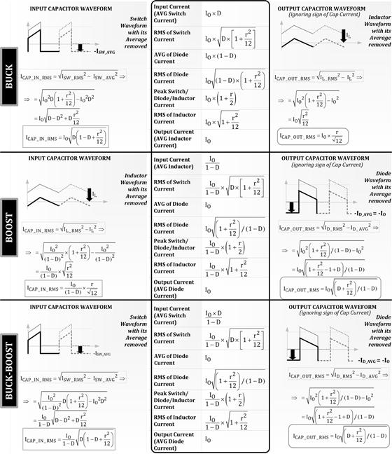
Figure 7.6: Calculating input and output capacitor current RMS values, based on tabulated current stresses.
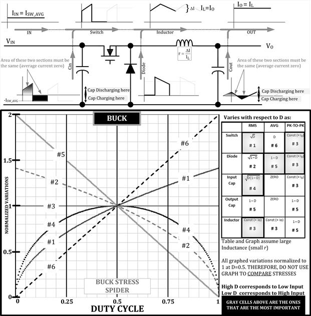
Figure 7.7: Current waveforms of a buck and its related stress spider.
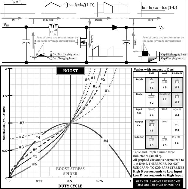
Figure 7.8: Current waveforms of a Boost and its related stress spider.
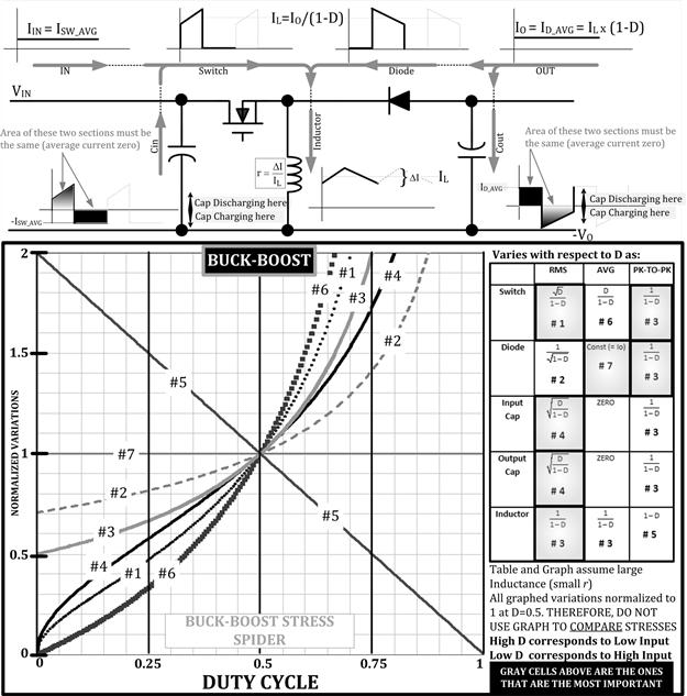
Figure 7.9: Current waveforms of a Buck-Boost and its related stress spider.
Some easy rules-of-thumb for selecting capacitors for a Buck converter are as follows.
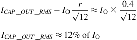
We have for the input cap (of a Buck)
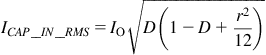
The function D×(1–D) has a maximum at D=0.5. Though the presence of the term in r affects this somewhat, we can simplify for low values of r
For example, a 3 A Buck will need an input capacitor sized to handle at least 1.5 A, irrespective of switching frequency, output voltage and so on.
In determining the worst-case RMS, we can ask: if D=0.5 is not included in the input range, what input voltage should we choose to check the suitability of the input cap of a Buck? The answer is: at the point closest to D=0.5. For example, if D varies from 0.2 to 0.4 over the given input range, we will pick the input voltage end at which D=0.4 (lowest input). If D varies from 0.6 to 0.8, we should pick the input voltage point at which D=0.6 (highest input). Of course, if D varies from 0.3 to 0.6, we will pick the input voltage where D=0.5 (i.e., VIN=2×VO).
We also realize that since RMS stresses do not depend on switching frequency, increasing the frequency will have no effect on the size of the input cap of a Buck! We can have a 2 MHz Buck as opposed to a 100 kHz Buck, but if we were using electrolytic input capacitors, both these converters will require the same input capacitor. But things can certainly change if we use ceramic input capacitors for example — these have such high ripple ratings that the acceptable input ripple, not the RMS rating, becomes the dominant criterion for selecting the input capacitor. Ripple, current or voltage, is a result of switching, and therefore does depend on frequency. So for example, in modern “all-ceramic solutions,” the input cap of a 2 MHz Buck can be roughly half the capacitance and size of a similar 1 MHz Buck. But we have to be careful too, since the use of ceramic caps on the input can cause overshoots and instability as discussed in Chapter 17. We also have to be careful in drawing too much meaning from the values of input caps shown in many semiconductor vendors’ typical schematics. The input cap of a Buck is rarely optimized as the output cap may be, and usually based on the “gut feel” of a typical engineer heading to the component cabinet. He tries it, it works, end of story.
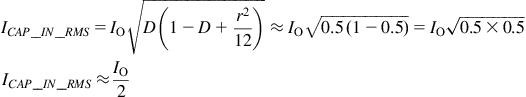
Why is the RMS rating not significant in selecting the output cap of a Buck? Because we know that the output RMS is very small in a Buck topology. Here is the rule-of-thumb for the RMS stress on the output cap of a Buck.
So, output ripple, not RMS, becomes the dominant concern, whether or not we are using electrolytic or ceramic capacitors. Now, the actual capacitance, not just the capacitor’s physical size as related to its RMS capability, becomes important, as also the parasitics of the cap (its ESR and ESL), which as we can see greatly affect the output ripple. Full derivations for capacitor ripple and its impact are provided in Chapter 13.
The Stress Spiders
One of our key learnings from previous chapters is that for a given output voltage, the duty cycle D, in effect tells us what the input voltage is. We also learned that in all topologies, a low D corresponds to a high VIN, and a high D to a low VIN. In the previous sections we have derived the RMS and average values of currents for all three fundamental topologies. We now want to know how the stresses vary with D, and thereby indirectly, with respect to the input voltage. Knowledge of that variation comes in handy in deciding at what voltage within the input range “worst-case” stress occurs and what that stress is, so we can apply the derating principles learned in Chapter 6 and correctly select the power components.
When we look at the RMS/AVG equations derived so far, we see they include both r and D. That makes the total analysis a little complicated since r depends on D (input voltage) too. To arrive at the “Stress Spiders,” in the following analysis, we have often used the “small r” (or “large L,” also called the “flat-top”) approximation. But only to a certain extent — in fact only where the term in r is insignificant — we then simply ignore it. But where r happens to be the dominant term, we do not ignore it, but use the following variations (as seen from the design table provided in the Appendix of the book).
Note that now we are also interested in the “peak-to-peak” currents. The peak-to-peak current in the inductor is simply ΔI. We want to know it because, for one, core losses depend primarily on peak-to-peak (and on the switching frequency of course, but not on IDC). Note also that in all topologies, the peak switch/diode/inductor currents are the same. That is important to know since we need to confirm that the inductor is rated for the peak current through it in terms of its rated ISAT or BSAT, so we can be sure to avoid core saturation, as discussed in Chapter 5. On the other hand, the RMS of the inductor current is important because it determines if the inductor is rated for that continuous RMS current value in terms of heat and its temperature rise. Note that in Figure 7.6, we have also provided the RMS of the “diode” current. The reason for that is, we may be using a synchronous topology, so we may actually have a MOSFET in place of the catch diode. To know the heating in a MOSFET we need to know its its IRMS, not its IAVG. Therefore, both IAVG and IRMS are provided for the diode (freewheeling) position.
We present some examples to show how we can approximate the dependency of the stresses with respect to D as displayed via the tables and graphs of Figures 7.7–7.9.
Example: Describe the dependency with respect to D of the peak-to-peak inductor current in a Boost topology.
The equation for peak-to-peak inductor current is
![]()
We know that the average inductor current (center of ramp) of a Boost is
![]()
Therefore, since r varies as D×(1–D)2 for a Boost, we get
![]()
This is the value displayed in the table inside Figure 7.8 and plotted out in the adjoining graph.
Example: Describe the dependency with respect to D of the output cap RMS current in a Boost topology.
From Figure 7.6, we have
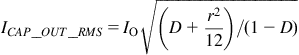
Therefore, assuming large inductances, the term in r is very small compared to D. Check: 0.42/12=0.013. If minimum D is about 10%, that is, D=0.1, the term in r is 10 times smaller. We can thus approximate (for a Boost)
This is the value displayed in the table inside Figure 7.8 and plotted out in the adjoining graph.
In this manner we get the three Stress Spiders shown in Figures 7.7–7.9. The salient points of these spiders are summarized below.
1. We had learned in Chapter 5 that VINMIN is a good point to select and design the magnetics of a Buck-Boost/flyback. Now from Figure 7.9, we see that almost all the stresses increase as D increases (low input). We realize that VINMIN is a good point to select, design, and evaluate the temperatures of all the power components too (of a Buck-Boost). In other words, during test and evaluation, we can just set “maximum load at lowest input,” and evaluate the entire Buck-Boost/flyback power supply for reliability and life requirements. One seeming exception is the peak-to-peak inductor current, which reaches a maximum at lowest D (high input). Admittedly, since core losses depend on ΔI, we may want to evaluate the choke at high input voltages too. However, core losses are usually a small part of the total choke (inductor) losses (especially in ferrites, as opposed to powdered iron for example). The dominant loss usually being copper losses, it is more common to measure the temperature of the magnetics of a Buck-Boost/flyback at its lowest input voltage, though in general, we may want to evaluate the temperature of the inductor at both the highest and lowest input voltages.
2. For a Boost, we can draw very similar conclusions as for the flyback/Buck-Boost above. VINMIN is the best point to start a Boost design too, and also for most of the other components and stresses. There is one small surprise here — the input capacitor’s RMS current has a max at D=0.5, not at the high or low extremes of input voltage. In this topology, D=0.5 is the point where VO=2×VIN (see Figure 5.9). Note that if in our application, the input range does not include the point VIN=VO/2, then for selecting and testing the input capacitor, we need to pick that end of the input range which lies closest to VO/2.
Note, however, that in a Boost topology, the input capacitor’s RMS current value is numerically very small compared to its output capacitor’s RMS. Because there is an inductor present between the input capacitor and the switch, which smoothens out the switch current waveform significantly, and that is what is finally presented to the input capacitor for completing the rest of the smoothening/filtering process.
That is why in all the tables in Figures 7.7–7.9, we have indicated the most important or significant stresses with a gray highlight. We can usually ignore the non-gray cells of the table. We emphasize that the Stress Spiders in the figures only express the relative variation of a particular stress with respect to its (own normalized) value at D=0.5. So, even though all the relative variations are overlaid on a single plot, each curve represents a completely distinct stress. We should not try to use the different curves of a Stress Spider to compare different types of stresses.
3. In a Buck, we have several surprises in Figure 7.7. Note that we have always advocated starting the design of a Buck converter at VINMAX. That indeed is a good point for designing and evaluating a Buck inductor. The inductor current has a constant center of ramp value equal to IO, which has an AC component riding on it that increases with input voltage. So the peak current is highest at VINMAX. The energy-handling capability of the Buck inductor, which depends on ![]() , must therefore be evaluated at VINMAX. Further, from Figure 7.7, we can easily deduce that the RMS of the inductor current (its heating) will also go up as input increases. So, the RMS of the inductor current of a Buck is also at its highest at VINMAX. We conclude that VINMAX is truly a good point to start the design of a Buck (the inductor). But is that good for all the power components of a Buck?
, must therefore be evaluated at VINMAX. Further, from Figure 7.7, we can easily deduce that the RMS of the inductor current (its heating) will also go up as input increases. So, the RMS of the inductor current of a Buck is also at its highest at VINMAX. We conclude that VINMAX is truly a good point to start the design of a Buck (the inductor). But is that good for all the power components of a Buck?
From Figure 7.7, we see that the switch RMS/AVG is the highest at high D (VINMIN) not at VINMAX. Intuitively this makes sense since at low inputs, the duty cycle increases, which means the switch is ON for a longer time, so it will tend to heat up more at low input voltages (higher stresses). That means the Buck switch must be evaluated for dissipation at VINMIN, not VINMAX. We can also conclude that if the switch is ON for a longer time, as at VINMIN, then obviously the diode must be ON for the shortest time at VINMIN. And therefore, the diode would be ON for the longest time at VINMAX. So, we expect the diode RMS/AVG will be worst-case at VINMAX. All this is borne out in Figure 7.7 from the Buck Stress Spider. In other words, the switch of a Buck (and its associated heatsinking) must be designed and evaluated at VINMIN, whereas its diode must be selected and checked for temperature rise at VINMAX. Note also that the RMS of the input cap is highest at D=0.5 (or the input end closest to it). So, we need to be careful in selecting and testing the input cap of a Buck. We see that it has been highlighted gray in Figure 7.7, and we realize it is certainly a significant term, numerically speaking, that we need to pay close attention to.
We can ask: how is it that in Figures 7.8 and 7.9, that is, for the remaining two topologies, the worst-case point for the diode RMS current is VINMIN, not VINMAX? That is because though the diode is still ON for a shorter time as input falls, the instantaneous (on-time) current through it goes up steeply as the input falls.
At this stage, the reader may like to look at the solved examples in Chapter 19, in which most of the equations derived above have been used in numerical examples.
Stress Reduction in AC–DC Converters
The AC–DC flyback is one of the trickiest converters to design reliably in a cost-effective manner. Let us first try to understand how to apply the RMS/AVG stress equations of previous sections to it.
(a) A flyback (transformer-based) converter can be reduced to a Primary-side equivalent inductor-based Buck-Boost converter for the purpose of selecting and evaluating the Primary-side stresses of the flyback. This means, the switch and input capacitor, in effect, “think” that they are part of a DC–DC Buck-Boost converter stage, whose input is the rectified AC input (~VAC×√2≡VIN), and whose output voltage is VOR=VO×n (Volts), with load current equal to IOR=IO/n (Amperes), where n=NP/NS.
(b) Similarly, the flyback converter can be reduced to a Secondary-side equivalent Buck-Boost for purposes of selecting and evaluating the Secondary-side stresses. Which means, the diode and output capacitor, in effect, “think” that they are part of a DC–DC Buck-Boost converter stage, whose input is the reflected rectified AC input (~VAC×√2/n≡VIN/n≡VINR), and whose output is VO (Volts) with load current equal to IO (Amperes).
To understand this better, see Figure 3.2 too. With all this in mind, we realize that all the current stress equations derived so far for the Buck-Boost can be easily applied to an AC–DC flyback.
Coming to the Forward converter, we consider its output section. Here we can assume the “Buck cell” (consisting of the two common-anode diodes, choke, and output capacitor) behaves as a DC–DC Buck converter whose input is the reflected rectified AC input (~VAC×√2/n≡VIN/n≡VINR), and whose output is VO (Volts), with load current equal to IO (Amperes). So, all the equations for current stresses that we have derived for the DC–DC Buck converter, apply to the Buck cell of the Forward converter too. On the input side of the Forward converter, the switch current (Primary side) was sketched in Figure 3.6. Note that it is very similar to the switch waveform of a DC–DC Buck converter with duty cycle D=VO/VINR (or equivalently VOR/VIN), with a load current equal to IOR=IO/n. The actual switch current is actually slightly more than the equivalent DC–DC Buck converter, due to the magnetization current component in the switch waveform, but since that contribution is very small compared to the overall waveform, it can be usually ignored.
Summarizing: similar to the mapping procedure described to go from an AC–DC flyback to a Buck-Boost, all the equations derived so far for RMS/AVG stresses for a Buck can also be quickly applied to the AC–DC Forward converter. So, the switch and input capacitor of the Forward converter, in effect, think that they are part of a DC–DC Buck converter stage, whose input is the rectified AC input (~VAC×√2≡VIN), and whose output voltage is VOR=VO×n (Volts), with load current equal to IOR=IO/n (Amperes), where n=NP/NS. On the Secondary-side, the free-wheeling diode and output capacitor of the Forward converter, in effect, think that they are part of a DC–DC Buck converter stage, whose input is the reflected rectified AC input (~VAC×√2/n≡VIN/n≡VINR), and whose output is VO (Volts), with load current equal to IO (Amperes).
One last component of the Forward converter that is not accounted for in the above mapping procedure is its output diode (the diode connected to the Secondary winding of the transformer). That diode conducts (only) during the on-time of the converter (with duty cycle D) and during that time it passes a current of average value IO (since we know that IO is the center of ramp of the Buck cell that follows). So, the average current through the output diode of the Forward converter, evaluated over the entire cycle, is IO×D. Multiplying that by the forward diode drop, gives the required diode dissipation.
If we have a two-switch (“2-switch”) Forward converter, the same current passes through each of its MOSFETs. So, we have to use the same IRMS value indicated above for each of the two MOSFETs, and then sum the two dissipations to calculate the total dual switch dissipation. So, in a 2-switch Forward-converter where each MOSFET has an RDS of say 100 mΩ, the total switch dissipation is twice that of a single-ended Forward converter with a single MOSFET of RDS 100 mΩ. The main advantage of using a 2-switch Forward is reflected in the fact that the voltage stress on each MOSFET is halved compared to a single-ended Forward, not the current stresses. It is also usually cheaper to find two 400 V MOSFETs with say, an RDS of x/2 ohms each, as compared to a single 800–1000 V MOSFET with an RDS of x ohms (same conduction loss).
See also Table 7.1 and Figure 7.2 to understand this better.
In Chapter 3, we discussed the zener clamp of a flyback as a means of reducing the leakage inductance spike of a flyback and thereby saving its switch from voltage overstress. Now, we look at another option of achieving the same basic result: the RCD clamp. Note that in a single-ended Forward converter, we may also have a leakage inductance spike due to the small leakage present between the Primary winding and the tertiary (energy-recovery) winding. However, these two windings are often wound bifilar (see Figure 9.22) and that helps the two windings couple well, reducing the leakage to near negligible. If not, some type of clamp or snubber may be required even for a Forward converter. For more tertiary winding aspects in the Forward converter, see Chapter 9.
RCD Clamps versus RCD Snubbers
Early power supplies used to invariably have an “RCD snubber” (also called a “dV/dt snubber”). RCD stands for resistor-capacitor-diode, and this little network would always be seen present across the switch. The purpose of an RCD snubber was two-fold.
(a) The RCD snubber helped reduce the transition overlap — between the voltage and the current belonging to the switch (in early days the switch was a BJT). This would therefore improve the dissipation (and temperature) related to the switch, though not necessarily improve the overall efficiency. For example, a lot of heat could be lost in the R of the RCD, instead of in the switch.
(b) The RCD snubber helped reduce the dV/dt appearing across the switch during the turn-off transition, thereby enhancing its reliability, especially when early MOSFETs appeared on the scene.
Today RCD snubbers are almost obsolete for several reasons: (1) BJTs are very slow and therefore rarely used, (2) modern MOSFETs are almost immune to dV/dt failures, and (3) switching transitions today are so fast, that though there is significant V–I overlap during the transition, the transition itself lasts for only about 50–100 ns every cycle compared to a couple of μs in early days (for overlap, see Chapter 8). In effect, the RCD snubber is history. In its place, the RCD clamp has surfaced.
RCD clamps are commonly used, especially in AC–DC flybacks. One reason is they can offer higher efficiency (and lower cost) than zener clamps (as discussed in Chapter 3). But that is conditional on the RCD clamp being very carefully designed. Note that on a schematic, an RCD snubber looks almost exactly like an RCD clamp to the untrained eye — the difference is a clamp uses a much higher capacitance (typically 10–47 nF) and a much larger R, whereas a snubber has a much smaller capacitance, rarely exceeding 1–2 nF, and a much smaller R too. Therefore, functionally speaking, the difference between an RCD snubber and an RCD clamp is as follows: whereas the capacitor of an RCD snubber fully discharges every cycle, the capacitor of an RCD clamp does not discharge fully between cycles, and remains always “pre-charged” — to just a little below its “clamping voltage level.” The RCD clamp capacitor therefore comes into play (i.e., the RCD clamp diode conducts) only above a certain Drain-to-Source voltage. Below that voltage level, the RCD clamp is virtually non-existent. When the RCD clamp diode conducts, because the capacitance of the RCD clamp is so large, it acts to literally “clip” the leakage inductance voltage spike of the flyback to a safe value. As mentioned, in contrast, the capacitor of an RCD snubber discharges fully every cycle, and when the switch turns OFF, the RCD snubber capacitor is immediately ready to accept part of the freewheeling current, thus lowering the dV/dt appearing across the switch (though also transferring the switch crossover dissipation into itself). The RCD snubber was therefore often called a “switching-aid network” — it literally aids the switching action. Whereas, an RCD clamp does just that: it clamps.
In Figures 7.10 and 7.11 we cover clamps in detail, in particular the RCD clamp. We derive the equations for calculating the R and C, and estimating the clamp dissipation. We also provide a numerical example. The important things to keep in mind are:
(a) The value of R is relatively independent of C, and yet is a key RCD design parameter by itself. In fact, C can be made almost as large as possible if cost permits (only its voltage ripple component will decrease; its average clamp voltage level will remain fixed since that depends on R, not on C!). The capacitance is typically chosen to be between 4 nF and 22 nF for AC–DC flyback converters switching between 70 kHz and 200 kHz. That value of C is such that the maximum voltage ripple that appears on it is below approximately ±10% (or the very purpose of the clamp gets defeated). However, a high value of RCD clamp capacitance comes in very handy under sudden overloads at high line, during which the clamp can receive a burst of excess energy, which could charge it up quickly and thereby threaten the Absolute Maximum voltage rating of the switch. If we do want to increase the C for such abnormal conditions, and/or have not properly designed the flyback protective limits (e.g., duty cycle max and current limit), we may want to play it safe by combining the RCD clamp with a paralleled zener clamp as indicated in Figure 7.10.
(b) The value of R is chosen carefully, and usually empirically. Its selection is purely based on not exceeding the Abs Max voltage rating of the switch under worst-case but steady operating conditions. R is obviously always selected at high line.
(c) However, the wattage rating of R is determined at the point at which its dissipation is at its maximum — and that occurs at low line.
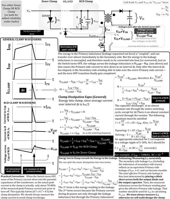
Figure 7.10: The RCD clamp explained, and derivations for R and C.

Figure 7.11: Connecting high Line conditions with low line, and thereby calculating R, C, and dissipation for universal input flybacks.
What are the key advantages of an RCD clamp over a zener clamp? Cost is one. Efficiency is another. The reason for the efficiency improvement of an RCD is explained as follows.
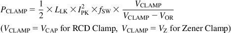
For example, when using a 700 V MOSFET, a 200 V zener clamp is often used, and the VOR is set to a maximum of 130 V. However, with a more cost-effective 600 V MOSFET, a 150 V zener is preferred, and the VOR is set to ~100 V. We saw in Chapter 3 that, provided the voltage rating of the MOSFET is not exceeded, if VCLAMP is made much bigger than VOR, the dissipation in the clamp falls. This is also obvious from the equation
For a zener clamp, the clamping voltage remains almost fixed (at 200 V and 150 V, respectively) with variations in line and load. However, using an RCD clamp, as we lower the input voltage (keeping load fixed at its max value), the clamping (capacitor) voltage rises on account of the higher switch currents — to ~220 V and ~170 V, respectively, at low line. And that lowers the clamp dissipation by about 20% as compared to a zener clamp under the exact same conditions. But we note that this efficiency improvement of an RCD clamp occurs only at low line and at max load. At lighter loads for example, the clamping voltage of an RCD clamp falls much lower than that of a fixed zener clamp, on account of the lower switch currents. Therefore, the efficiency at light loads using an RCD clamp is worse than a zener clamp. Intuitively, we can view the RCD clamp as a “bad” zener clamp whose clamping (zener) voltage depends rather steeply on how much current we push into it. That helps in reducing clamp dissipation, but it can lead to excess voltages too. Therefore the RCD clamp design is rather critical. As mentioned, some nervous engineers end up combining both the RCD and zener clamps in parallel as indicated in Figure 7.10.
In designing RCD clamps there are two key optimization details to keep in mind as also discussed in Figure 7.10.
(a) The measured current into the clamp at the instant of switch turn-off is actually 70–80% of the peak switch current just prior to turn-off. This is because part of the free-wheeling Primary-side current goes into the interwinding capacitance of the transformer, from where it eventually gets (largely) dissipated as heat in the windings. The actual clamp dissipation, being proportional to ![]() , is therefore 50–66% of the theoretical estimate. This knowledge helps us to not overdesign the clamp. Very few simulation models will tell you this — bench measurements are very revealing here.
, is therefore 50–66% of the theoretical estimate. This knowledge helps us to not overdesign the clamp. Very few simulation models will tell you this — bench measurements are very revealing here.
(b) The leakage inductance on both the Primary and Secondary sides serves to slow down the transfer of current from Primary to Secondary side, thereby extending the duration Δt (see Figure 7.10). This is the duration in which Primary-side current freewheels into the clamp waiting for all leakage inductances to either discharge or charge up as required, in going from one switching state to the other. So, the two inductances must be clubbed together to estimate Δt correctly.
The best way to determine the effective Primary-side leakage LLK for use in the clamp dissipation equation is to do an in-circuit measurement. We need to place thick shorts across the output diode and the output capacitors, and then measure the inductance across the Primary winding pins. That reading gives us the correct LLK to use. But for this method to succeed, the prototype must already be available. An alternative and surprisingly accurate estimate in the initial design stages is:
![]()
where LLKS=20 nH/in.×(length of Secondary-side traces in inches).
Here we have used the empirical fact that a “good” AC–DC flyback transformer (say, with a split Primary, each half containing NP/2 turns, sandwiching the Secondary windings containing NS turns) has a typical leakage equal to ~1% of the Primary inductance (the inductance across the Primary winding with the Secondary winding open). Also, the main contribution to the Secondary-side leakage (which then reflects on to the Primary side as turns ratio squared) actually comes from the Secondary-side PCB traces, not the transformer (which is the reason why an in-circuit estimate of leakage is recommended). We know that PCB traces result in about 20 nH/in. We also need to numerically add up the total forward and return PCB trace lengths right up to the first output capacitor and use that to find LLKS based on the 20 nH/in. rule. Note that after the first output capacitor of the flyback, we have mainly DC current and so the trace inductance is not relevant anymore.
For a given VOR, the turns ratio of low-voltage output rails is much higher, because by definition, VOR=n×VO. Since Secondary-side leakage reflects to the Primary side as n2, it can become almost as large as the Primary-side leakage LLKP — especially where the turns ratio is high (as for low output voltages). Therefore, a good rule of thumb is to simply take LLK as being not just 1%, but 2% of LP — for the purposes of determining R and PCLAMP.
Now we also understand why a 70 W flyback with only a 12 V output rail present, will “mysteriously” exhibit a much higher efficiency than a 70 W flyback with only a 5 V output rail — despite having the same VOR, VCLAMP, and even LLKP in both cases. The difference is due to the turns ratio, which leads to much higher clamp dissipation for the 5 V output.
A way to improve overall efficiency rather dramatically, especially for low-voltage output rails, is to try to cancel the inductance of the forward and return Secondary side traces. That will reduce clamp dissipation significantly. For that we need to run the forward and return traces very close and parallel to each other. By doing so, the fields produced by the current flowing in opposite directions cancel, and the inductance reduces (no field — no stored energy — no inductance). That field cancelation happens automatically when using a multilayer PCB with a wide ground plane right below the traces. And that is why double-sided PCBs automatically tend to offer superior efficiency compared to (sloppily laid-out) single-sided PCBs in low-output universal input flybacks.