7
Solid State Disks
The technologies surrounding solid state drives (SSD) have been in use for at least a couple of decades. Until recently, seldom were there mainstream SSD applications for the enterprise or data center, nor were there many practical uses of SSD in storage subsystems for professional moving media applications. As the cost of flash memory began to drop dramatically in the later part of the previous decade (ca. 2008–2009), and the storage size of memory modules began to grow, the implementation of SSD systems began to increase.
SSD may stand for either solid state disk or solid state drive. Purists would argue that it cannot be a disk because that would assume it has a form of “disk” media that spins. Perhaps, it is assumed that because SSD is evaluated in competitive terms against the HDD, and depending upon the system, may use the same SAS, SATA, or Fibre Channel storage interfaces, that the SSD really is not just a disk—more appropriately it is a drive.
Regardless, this chapter will look at the SSD as a formidable type of storage, one that offers many advantages to magnetic or optical spinning disk storage systems, not the least of which is power consumption, reduction of access time, and resistance to shock.
Irrespective of SSD’s advantages and capabilities, which are covered in this chapter, a looming question still remains: As the storage industry takes a hard look at cost-control and its environmental ecosystems, just how soon will the move to SSD accelerate for enterprise level implementations?
KEY CHAPTER POINTS
•An overview, history, and development of flash memory, which is the media form utilized in solid state disks
•The components, cell structure, and operations of flash memory
•Outlining the values and the limitations of flash memory
•The designations, applications, and differences between NOR and NAND memories
•How data protection and security are handled in solid state disks
•Applications for flash memory and the components in a solid state disk
Solid State Storage Evolution
In an era of increasing file sizes, megalith-like storage requirements, rotational disk drive capacities exceeding terabyte proportions, and an astounding dependence upon storage in dimensions previously unobtainable comes a restoration of a nearly lost technology—solid state memory for mass storage.
The evolution of flash-based memory for consumer and professional applications has helped drive a renewal in solid state, scalable enterprise storage. Various memory technologies have been developed to address differing applications for solid state disk data storage. One of the dividing lines in memory is whether it is volatile or non-volatile in nature. Hard drives are for the most part non-volatile. That is, once the magnetic state is set (i.e., to a one or a zero), that state is maintained unless some significant catastrophic outside force alters that state.
While hard drives solve the majority of the volatility issues, other physical constraints create another level of encumbrance.
Limiting Factor
Since the early days of mechanical storage on magnetic spinning disks, the physical properties associated with the storing and retrieving of data from the disk platters have continued to be a performance-limiting factor. Despite myriad advancements over the years in hard drive technology, the issues of seek time latency that accompany the spindle speeds, armatures, and head assemblies have continued to place restrictions of the accessibility of the data.
Fundamentally, the management of disk-based storage is governed by the physical structural requirements surrounding the depositing and recovering of data bits that lie in a series of lineal concentric tracks around the surface of the platter. This data, organized as blocks, are tracked in a tabled sequence of pointers that are controlled and arranged by a combination of resident firmware and additional third-party software, which is overseen at the application layer by the disk operating system.
Hard disk drive management methodologies differ from the approach utilized in solid state memory.
Dynamic Random Access Memory
The first type of solid state memory technology to gain any noteworthy foothold at the enterprise level was the Dynamic Random Access Memory (DRAM) SSD.
DRAM should be noted as a volatile memory technology. DRAM utilizes capacitors to store data, which are required to be continually refreshed (via electrical power) in order to preserve the data state of each memory element. Thus, a DRAM SSD’s drawback is that if power is removed, the capacitor’s state cannot be refreshed and the data are lost.
Manufacturers, in their effort to address the volatility issues, will typically build-in an alternate power source such as a back-up internal battery to enable the refresh state and preserve the state of memory. DRAM SSD technologies may employ the movement of data to a secondary HDD, or to another flash-based memory system as a data protection scheme should a power failure event occur.
An advantage of DRAM SSD is that its access is completely random. Each cell is addressed in an X-Y fashion for both read and write operations. In terms of data access speed, DRAM SSDs remain the fastest technology as they performs both reads and writes at approximately the same speed. This makes their principle selling point performance.
The drawback to the DRAM SSD is that it has a greater power requirement, which may be seen as cost prohibitive for most enterprise-level applications. This in turn creates an opening for cheaper flash-based, energy-efficient SSD technology.
Flash Memory
Flash, as a form of non-volatile memory (NVM), can be electrically erased and reprogrammed. Flash memory has recently appeared in products for professional video media serving applications including video on demand, cache, and near term/near line storage. In the NVM category, flash memory is the technology of choice versus DRAM because in flash, the storage cells retain data whether power is applied or not.
Flash memory has become the core element in SSD technologies, replacing the concept of DRAM SSD, which first showed its applicability in the early 1980s.
Development
Flash development began in the mid-1980s when Dr. Fujio Masuoka, working for Toshiba, presented his invention to the 1984 IEEE Integrated Electronics Devices meeting held in San Jose, California, USA. It was not long before Intel recognized the tremendous potential and began production by introducing the first commercial NOR type flash chip in 1988. CompactFlash was originally based on it, though later cards moved to less expensive NAND flash. Toshiba announced NAND flash at a developers meeting in 1987.
The solid state disk (drive) had origins going back as far as the 1950 where two memory technologies (core memory and card capacitor read only store [CCROS]) were being used in vacuum tube-type computers. By 1987, a 16 kilobyte RAM-based solid state drive was introduced by Texas Memory Systems, with others, including StorageTek and Sharp. Showing implementations throughout the early to mid-1980s.
The introduction of flash-based SSD came in 1995, and by 2009 at 1 TB flash SSD was in the production chain offering 654 Mbytes/second (maximum) write speeds and 712 Mbytes/second (maximum) read speeds. The same year saw a 6 Gbits/ second SATA interface SSD from Micron Technology.
Flash Memory Functionality
Data are stored in flash memory as an array of floating gate transistors called “cells.” Each cell traditionally stores one bit of information. Subsequent generations of flash memory devices, referred to as multi-level cell devices, are capable of storing more than one bit per cell by varying the number of electrons placed on the floating gate of a cell. Manufacturers touted their respective products based upon how their particular versions of flash cell technologies were implemented.
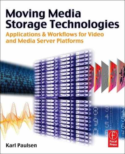
Flash utilizes cell-based floating-gate transistors that will store a charge for an extended period of time, even when no power supply is connected (see Fig. 7.1). These memory cells are similar to an electronically programmable read-only memory (EPROM). The cell technology employs a thin oxide insulation that surrounds the floating gate and traps the charged electrons. This insulation prevents leakage, which is a loss of charge state once power is removed.
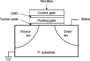
Figure 7.1 Flash memory cell.
Floating Gate Charges
The flash memory cell functions by storing a charge in the floating gate. The presence of charge determines whether the channel will conduct or not. During the read cycle, a logical 1 at the output corresponds to the channel being in its low resistance. This is referred to as its ON state. The control gate is used to charge up the gate capacitance during the write cycle.
Serial Access
Unlike the X-Y addressing in DRAM, flash access must be in serial fashion. Flash further relies on a controller to bring the data out of the chip and correctly present it to the processor.
NAND and NOR
Flash memory will be categorized like conventional logic. It can be either in a NOR-gate like configuration, first available around 1987, or as a NAND-gate model, which was developed in the 1988–1989 timeframe. Fundamentally, the distinctions between NOR and NAND are described by
•speed of access and/or erasure
•how individual memory cells are connected (NOR is parallel, NAND as serial)
•how read-write interfaces (page based versus randomly accessible) are facilitated
NOR-gate Flash
NOR flash memory requires a long time period for both its erase and write cycle operations. A positive attribute for NOR flash is that it provides full addressing to data buses, permitting random access reads and programming to any memory location. Furthermore, its value is that it will endure between 10,000 and 1,000,000 erase cycles.
NOR flash memory’s drawback is that complete random access rewrite or erasure operations are inhibited because any individual memory cell’s state can only be changed from its native state (as a logical 1) to its opposite state (a logical 0). Successive writes that change a cell’s bit from logical 1 to logical 0 are permitted, but returning a single memory bit in a cell to its native state (logical 0) must be accomplished by an erasure of an entire block; that is, all the bits must revert to a logical 1.
Similar to common memory, the NOR read-only mode is provided by address and data bus mapping. Like other addressmapped memory, NOR flash memories can be used as executein- place (XiP) memory, behaving as a ROM memory mapped to a certain address. XiP memory is a requirement for most embedded systems.
The unlocking, erasing, and writing processes for NOR memory use special commands that are written to the first page of the mapped memory. As defined by Intel, the commands (called the “common flash interface”) provide a list of all available commands to the physical driver. Apart from being used as a read-only memory (ROM), NOR-based flash memory may also be partitioned with a file system and may be further used in almost any solid state storage device.
NAND
NAND flash followed NOR development in 1989, which came principally from Samsung and Toshiba. NAND exhibits both faster erase and write times, higher density, and a lower cost-per-bit compared with NOR flash. NAND flash, also known as NANDgate flash, endures 10 times the erase and write cycles of NOR flash. The core of most removable USB flash drives use the NAND flash memory format.
NAND flash’s disadvantage is in its input/output (I/O) interface, which allows only sequential access to data. While this makes NAND suitable for mass-storage devices such as PC cards and various memory cards, some believe it is less useful for computer memory.
NAND flash uses tunnel injection for writing and tunnel release for erasing. Tunneling is the principle of injecting charge carriers (i.e., the electrons and holes of solid state physics) to an electrical conductor through a thin layer of an electric insulator. The I/O for NAND flash memory cells are not individually random accessible. Thus data, arranged as pages, must be addressed in blocks, much like how hard disk drives are organized. Reading and programming is accomplished on a page basis; however, erasure must occur in complete blocks.
NAND flash memories are incapable of providing execute-inplace (XiP) memory operations due to their physically different construction principles.
When executing software from NAND memory, virtual memory strategies are used. When used in this fashion, memory contents must be paged into memory-mapped RAM and then executed from there. This requirement makes the presence of a memory management unit (MMU) on the system a necessity.
NAND versus NOR
NOR flash has no shared components and is more expensive to produce. It is found mainly in consumer and embedded devices such as cell phones, smart devices, and PDAs.
NOR provides faster read speed and improved random access capabilities. However, NOR technologies, such as write and erase functions, are slow compared to NAND. NOR has a larger memory cell size than NAND, limiting scaling capabilities and therefore achievable bit density compared to NAND. Figure 7.2 shows the structures for NAND, AND, and NOR cells.
NAND offers fast write/erase capability but its sacrifice is that its read speed is slower than NOR. Nonetheless, NAND memory is more than sufficient for most consumer applications such as digital video, music, or data storage. Because of NAND’s fast write/erase speed, its higher available densities, and its lower cost-per-bit compare with NOR, many feel that NAND memory makes it a more favorable technology for file storage, consumer applications, and SSD applications.
NAND offers over 5 Mbytes/second of sustained write performance. The block erase times are an impressive 2 ms for NAND versus 750 ms for NOR. While NAND has several significant positive attributes, it is not well-suited for direct random access.
Offering users the ability to rewrite data quickly and repeatedly, NAND is typically used for storing large quantities of information in devices such as flash drives, MP3 players, multifunction cell phones, digital cameras, and USB drives. NAND flash memory continues to increase its inroads into the enterprise storage domain, especially in applications such as SSD.
Cell Structures
An important consideration for enterprise users is whether NAND flash memory is of a single-level cell (SLC) or multilevel cell (MLC) configuration. Although the less-costly MLC flash can store twice, as two or more bits per cell and multiple levels of charge, it does not perform as well and is less reliable than SLC.
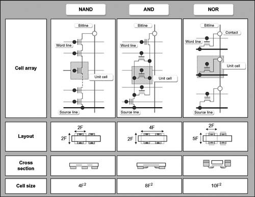
Figure 7.2 Cell structures for NAND, AND, and NOR configurations.
Single-Level Cell
One of the preferred SSD technologies uses flash memory known as single-level cell (SLC). This technology is currently favored by many vendors producing storage systems aimed at enterpriselevel data needs. In SLC NAND flash, each memory cell stores an analog representation of the data and two levels of charge.
SLC is said to be the dominant flash memory technology for SSD used in enterprise storage systems today, with estimates stating that SLC factors into more than 80% of enterprise-grade memory applications.
Multi-Level Cell
Multi-level cell (MLC) flash stores multiple bits per cell. MLC NAND, however, requires error correcting codes (ECC) to ensure data integrity. MLC NAND has the benefit of being cheaper due to the denser storage method used, but software complexity can be increased to compensate for a larger bit error ratio (BER).
Figure 7.3 The NAND device’s memory structures, input- output paths, and data area allocations.
NAND flash (see Fig. 7.3) includes extra storage on each page, found in a spare area of 64 bytes (16 bytes per 512-byte sector). This area stores the ECC code as well as other information like wear-leveling or logical-to-physical block mapping. ECC can be performed in hardware or software, but hardware implementation provides an obvious performance advantage.
Pages and Blocks
Groups of cells are organized into pages, the smallest structure that is readable/writable in a SSD, with four kilobyte pages standard on SSDs (refer to Figures 7.4 and 7.5).
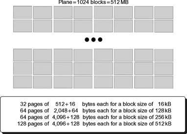
Pages are grouped together into blocks. It is common to have 128 pages in a block, which is equal to 512 kB in a block. A block is the smallest structure that can be erased in a NAND-flash device, so while you can read from and write to a page, you can only erase a block (i.e., at 128 pages at a time). This is one of the most important parts of understanding SSDs.
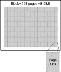
Figure 7.4 Page/block arrangement for the NAND cell.
Arrays of cells are grouped into a page; arrays of pages are grouped into blocks. Blocks are then grouped into planes. There are multiple planes on a single NAND-flash die. There can be multiple dies in a package (i.e., two or four per package), and multiple packages can be layered atop one another.
Error-Correcting Codes
Error-correcting codes are schemes that allow for the integrity of random data to be retained as the data are recovered from a storage system, transmission, or the like. The principal idea for achieving error detection and correction is to add redundancy in the form of extra data to a message. The device (e.g., a receiver) then uses this redundancy to check for the consistency in a delivered message or bit stream. Error-detection and correction schemes can be either systematic or non-systematic.
In data storage systems, the more common practices use such schemes as repetition codes, parity bits, check sums, cyclic redundancy checks (CRC), and error-correction codes (ECC). Providing schemes like ECC in hardware or software elevates the robustness of the system.
For MLC NAND memory, during a programming operation, the ECC unit calculates the error-correcting code based on the data stored in the sector. The ECC code for the respective data area is then written to the respective spare area. When the data are read out, the ECC code is also read, and the reverse operation is applied to check that the data are correct.
Figure 7.5 NAND cell block and plane arrangement.
It is possible for the ECC algorithm to correct data errors. The number of errors that can be corrected will depend upon the correction strength of the algorithm used. Simple Hamming codes provide the easiest hardware implementation, but can only correct single-bit errors. Reed-Solomon codes can provide a more robust error correction and are used on many of today’s controllers. BCH codes (used to correct multiple random error patterns) are also popular due to their improved efficiency over Reed-Solomon.
Block Management
NAND flash’s block management is provided by software, which is responsible for wear-leveling or logical-to-physical mapping. This software may also provide the ECC code if the processor does not include ECC hardware.
The large die size used in NAND fabrication results in some NAND devices shipping from the factory with some bad blocks. The software managing the device is responsible for mapping the bad blocks and replacing them with good blocks. These blocks are mapped in such a way that the software can scan all the blocks to determine where the good blocks and bad blocks are located. Initialization software simply scans through all the blocks to determine which are bad and then builds a table of bad blocks for future reference.
Special care must be given not to erase the bad-block marks originated by the factory. Some blocks marked bad at the factory may be functional at certain temperatures or voltages but could in other conditions fail sometime in the future. Once the badblock information is erased, it cannot be recovered.
Preventing Wear Out
Given that NAND flash memory chips will wear out after successive writes, it is imperative that frequent data accesses do not occur on a single or limited number of flash chips. To mitigate this wearing out, flash SSD manufacturers incorporate solutions that abstract the physical storage layer from the logical layer. Though a computer system will write data to the same logical address every time, the software engineering of the flash controller will move the underlying physical address around to the least written blocks on flash memory chips or least written locations within the chip. This process is known as “wear leveling.”
A unique characteristic of flash blocks is that if they are bad, writing to that block will fail. This problem is easily detected by the flash controller, which then will write the data to a different flash block and remove the bad block from any future write or read actions.
NAND Flash Memory Applications
Promoters and analysts say that single-level cell is the dominant flash solid state drive technology in enterprise storage systems. While SLC drives, which only store one bit of data per cell, are benchmarked as being longer-lasting and more reliable than MLC, the MLC drives store multiple pieces of data per cell; thus, they can deliver a higher storage capacity per unit area.

The use of MLC technology can lower the cost of memory storage systems, as was the case for memory cards (per examples in 2005); the final retail price of an MLC flash card was as much as one-third less than SLC cards of the same capacity. For consumer applications in video recording and playback, higher speed SLC flash offers no serious advantage, whereas the lower cost of MLC flash can be a significant asset. Table 7.1 compares the functional distinctions between SLC and MLC NAND flash.
Performance
The performance of flash memory typically considers three parameters:
•read speed
•write speed
•endurance
For consumer audio and video applications, read speed is important during the playback of stored audio and video, and is equally important in the retrieval of data files from mass storage. However, write speed is just as significant a factor in the recording of audio and video signals to ensure bits are not lost and that continuity of the images is consistent.
Endurance, described as the number of write/erase cycles a flash memory cell can tolerate, impacts the useable lifetime of a device. MLC flash memory meets or exceeds the requirements of consumer applications in all three categories.
Real-Time Video
One of the most demanding applications from the standpoint of read and write performance is the recording and playback of video and audio signals, such as in a digital camera or digital video recorder. Performance levels will depend on the video quality desired from the compression format and bit rates selected.
High-definition (HD) video signal recording may use either MPEG-2 or MPEG-4 compression, or other semi-proprietary or standardized compression schemes based on MPEG or other concepts.
MLC flash memory, for example, those made with a 90 nm process and using large-block architecture, achieve a read speed of up to 108 Mbits/second. This is fast enough for four times or faster playback speeds. With a write performance of up to 20 Mbits/second, real-time MPEG-2 video recording at HD quality is obtainable.
While SLC flash systems can have slightly higher read performance (e.g., up to 128 Mbits/second) and typical write performance of up to 45 Mbits/second, the performance differences do not necessarily add significant value in video recording or playback.
Audio Applications
Portable MP3 players fall well within the read and write performance of MLC flash. Even for full CD quality stereo, audio recording and playback will only require approximately 0.124 Mbits/ second of storage bandwidth.
Access to Data
In any storage system, data access is a performance criterion that has a direct impact on the return on investment in terms of time, reliability, repeatability, support, and maintenance. SSDs are devices that can clearly change the perspectives regarding access.
Stress Testing
As a benchmark comparison, solid state disk access times can be as much as one hundred times faster than that of the fastest spinning hard disk drive.
To understand how the parameters surrounding data access are quantified, a stress test would be generated that exercises the storage components against known benchmarks from another system. In computer programming, the “Create, Read, Update, and Delete” (CRUD) model is used to test and evaluate persistent storage. This test model is sometimes modified to suit the particulars of the media that is being stressed. Database operations will often use stress test analysis because they will typically search for, retrieve, modify, and then replace data that are located all over the storage system or systems and, at the disk level, all over the surfaces of the drives themselves.
When analyzing performance in a database application, one stress test conducted over a 24-hours period involved both reading and writing in a sequential and random fashion with 4K, 8K, 16K, 32K, and 64K I/O block sizes structured with 25 different workloads. The claimed performance of one SSD was equivalent to the performance of 10–16 Fibre Channel hard disk drives.
SSD Latency
Latency is one of the biggest issues in assessing hard drive performance. Even with the newest forms of 2.5-in. HDD storage, the problem of latency in SSD becomes a non-issue. SSDs, when configured as RAM disks, have incredible IOPS (input—output operations per second) numbers, which fall on the order of 70,000 to upwards of 100,000–250,000 IOPS.
An average enterprise-class 15,000-rpm hard drive achieves between 350 and 400 IOPS. The average enterprise-class SSD pushes 80,000 IOPS, a 200-fold increase. Such performance benefits outweigh the cost differential in certain instances, particularly when factoring in savings from energy costs.
Applications requiring extremely fast location and/or retrieval of data, such as online credit-card transactions, video on demand, or information-heavy Web searches, will benefit from solid state technology.
Block-Locking Protection
Protection of the non-volatile data in a flash device has always been an important consideration. Flash memory products feature dynamic hardware block locking, which keeps critical code secure while non-locked blocks are programmed and erased.
The block-locking scheme offers two levels of protection. First, it allows software-only control of block locking, which is useful for data blocks that are frequently changed. The second protection level requires hardware interaction before locking can be changed. This aids in protecting infrequently changed code blocks.
Locking capabilities may be employed differently depending upon the product family.
Security
At the forefront of many applications is security. As an example, certain flash products may be equipped with two 64-bit onetime pad (OTP) protection registers. OTP registers are used to increase system security. Intel programs a unique, unchangeable 64-bit number into one of the OTP protection registers, and the end user (as desired) can program the other 64-bit register. Once programmed, the end user’s segment can be locked to prevent further reprogramming. The OTP information can also be used as a small-encrypted security key for system authentication, or for manufacturing traceability.
Solid State Disk Applications
The use of flash memory and SSD has increased many fold since the period beginning around 2005.
Flash memory has some obvious advantages over DRAM or disk storage. Flash can store orders of magnitude more data in the same physical footprint as DRAM. Its reliability is extremely high, as much as 100 times better than a disk drive. Flash’s access time is approaching 250 times that of spinning disks’ access times.
RAM-Cache with Flash
When looking at system architectures, a mixture of RAM-cache with flash support is not uncommon. The combination of RAM and flash aids in balancing buffer speeds for an all SSD or flashbased storage subsystem.
Flash SAN
In this RAM-cache form, the application of RAM—with its extremely fast read and write performance—may support between 10% and 15% of the temporary storage cache, with the balance of the SAN utilizing flash only. This model will find that the RAM is used mainly for buffering, with the principle data content residing in non-volatile flash memory. Since flash can be read very fast, compared to its write times, moving assets from “permanent” flash storage to RAM can be managed on a demand basis. Populating the flash storage component can happen directly from the input stages of the storage system, or when demands or vulnerability warrant, by employing a combination of the RAM buffer into the flash memory.
SSD products now provide comparative performance capabilities to that of 15,000 RPM spinning disk SANs. In production as of mid-2009, this showcases how flash SANs compare to traditional spinning disk SANs, which offer sustained I/O rates of only around 300 IOPS.
Houston, Texas based Texas Memory Systems (TMS) offers a 5 TB flash SAN in a 2U chassis that draws less than 230 watts of power. The flash SAN utilizes SLC NAND flash to provide shareable, high-performance storage for IT organizations. TMS’s RamSan-620 has extremely low latency, with sustained I/O rates up to 250,000 IOPS (at 4K block sizes) for reads or writes, with random bandwidth up to 3 Gbytes/second. The system employs dual ported 4-Gbit Fibre Channel controllers, or may be equipped with one to four DDR InfiniBand ports. Each flash card in the TMS RamSan-620 includes on-board RAID protection to protect against chip failure.
In addition, an advanced chip-level ECC provides multiple regions of bit correction per block. A more recent product (RamSan-63) features 4–10 TB of flash storage, with 500,000 IOPS and 8 Gbytes/second randomly sustained throughput. This unit consumes only 450 watts making this type of application ideal for lowering the total cost of operations (TCO) and for green data center storage environments.
Flash NAS
USB dongles are one of the more familiar applications of solid state memory technology. A typical implementation may be a USB 2.0 as an FTP server or Secure Digital (SD) card. Data transfer is in the area of 10 Mbytes/second with up to 2 TB of storage using a FAT32 file system.
Flash-Based Protection
Flash-based stores can be protected in similar means to their rotational spinning disk counter parts. RAID techniques, such as RAID-3 or RAID-5, are deployed using specially purposed single or dual controllers that manage the striping in similar fashion to RAID-3 for hard disks.
Video serving applications may employ the same kinds of RAID protection, usually in software, including ECC-parity and secondary hot standby drives or additional second parity drives. While complete mirroring, as in RAID 1, is another alternative, it carries with it double the cost.
Justification
There may still remain some arguments that are difficult to dismiss. Even with 64 Gbyte flash memory, in a single stage environment it may be hard to justify flash versus the cost of a single 1 TB hard disk drive. However, to gain the bandwidth and throughput necessary for a conventional professional or broadcast videoserver storage system, some still feel that other sets of components need to be included in addition to a dedicated or single SSD-array configuration.
Concurrent Users
One further justification is that when implementing solid state storage, one finds that it typically relieves I/O bottlenecks, which allows processors to run closer to maximum throughput. Conventional thinking suggests that adding concurrent users requires adding more servers, but with solid state storage (i.e., with SSD), the number of concurrent users scales as a result of improved server efficiency.
Flash-Only Solution
The “flash-only” solution may not yet be viable for those mission- critical, large file size systems found in broadcast play-out operations. However, new implementations for products using flash are being introduced that could change that landscape. These flash-based servers now make up components including supplemental edge servers, caches, or video on demand (VOD) applications.
Cost
Any time a reference to the cost of storage is printed, it can immediately be presumed as “out-of-date,” just because the technology and the cost to manufacturer scale proportionately. That said, despite declining prices, SSDs remain far more expensive when put on a cost-per-gigabyte basis, at about 10 times that of a hard disk drive.
Nonetheless, depending on performance, SSDs can range in cost from $3 to $20 per gigabyte. Comparatively, hard drives range in price from 10 cents per gigabyte on the low end to between $2 and $3 per gigabyte for enterprise-level, 15,000-rpm models. This puts SSD versus HDD pricing at about 20:1 for the bottom end of both technologies. Analysts expect that this will stay in effect for the next several years.
In recent times, the cost of NAND memory has seen a 50% drop, but there is still little cost advantage when comparing bytes of HDD to bytes of SSD. However, the “cost-per-gigabyte” factor is not the most important one when looking at some of the accessheavy data center applications. Here, it is the cost per IOPS that becomes the benchmark to beat.
Portability and Green Perspectives
With operational costs high on the agenda of businesses, utilizing SSD technologies in certain applications will significantly reduce the power consumption for the physical storage system and for the supporting cooling requirements as well. Data centers are recognizing this, and where there are demands for access of data on a repeated basis, or for short-term cache activities, adding SSD RAM-disk devices will help reach these targets.
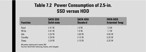
When portability is required, SSD power consumption becomes an equally important factor (see Table 7.2). SSD will use far less energy than traditional HDDs because there are no motors to drive in a SSD. It is true that the hard disk industry has taken steps to address power requirements by implementing idle drive spin down, and through the development of hybrid HDDs, but even with these implementations, most regular HDDs will consume more power than a SSD.
Applications for SSD
The high-level storage performance, ruggedness, and reliability of MLC NAND flash technology will support the increased mobility and functionality of a wide range of consumer electronics and a growing number of professional video applications.
Online transactional processing, streaming video on demand, and even virtual desktop infrastructures (e.g., netbooks and tablet computers) can make excellent use of SSDs. The devices are available in the popular form factors and capacities exist for a variety of computer and memory applications. The 2.5- and 1.8-in. form factors found for many SSD devices help squeeze these devices into space-starved products.
Blade servers are using SSDs to increase throughput, and to reduce the footprint on a card-by-card basis. The rise in multicore processor blades is increasing the demand, and the viability, for SSD.
Late generation 32 nm NAND flash in mSATA and Half-Slim modules lay claims to providing greater design flexibility, as well as space and cost savings when compared to SSDs with hard disk drive form factors and cases. These kinds of modules are available in 1.8-in. form factors with capacities up to 128 Gbyte, helping to bring the performance advantages of SSDs to notebooks, portable electronics, and embedded systems.
Toshiba’s high-performance HG3 series 32 nm solid state drives are available in capacities up to 512 Gbyte with sequential read speeds up to 250 Mbits/second, and these are useful for computing applications and a variety of other storage solutions.
Bitmicro’s E-Disk technology offers 800 Mbytes/second full duplex burst rate and storage capacity of up to 1.1 TB in a Fibre Channel (4 Gbit, dual port) interface. A write endurance of over 76 years with 100 Gbytes/day erase/write cycles puts this kind of technology squarely in the face of the future.
Supplementing Video on Demand with SSD
Streaming movies to thousands of users is a daunting task requiring a high number of servers capable of delivering a huge volume of streaming media files. The challenges associated with video on demand (VOD) that related directly to performance problems include the high number of concurrent users and the randomness of content access.
VOD systems are prominent from hotels to cable systems to the Web. These installations are guaranteed to see periods where there will be a very high number of concurrent users, especially with new releases or specials. Streaming video is typically a relatively easy task for hard disk drive videoserver systems where sequential access to contiguous data is the only operation they are doing. Conversely, VOD does not result in sequential disk accesses. VOD allows users to access stunt features such as start, stop, pause, rewind, and fast-forward. Compound these issues with multiple concurrent users and access to the stream becomes completely random. This is the most stressful activity for VOD servers.
Moving the most highly accessed content to a SSD designed for video on demand can significantly reduce access issues. The SSD application, in this case, augments but does not necessarily replace the disk-based VOD system. This high-demand content can be shared across multiple VOD servers without contention. The additional SSD bandwidth provides a good fit for large VOD installations.
Set-Top Box and D VR F unctionality
SanDisk and NDS, leading providers of technology solutions for digital pay-TV, announced in September 2010 that NDS successfully combined set-top box software and solid state drives enabling a new range of lower cost set-top boxes (STBs) with DVR-like functionality. The new solutions allow for the deployment of energy-efficient STBs with decreased power consumption, small form factors, and virtually silent operation.
The robust performance needed for video consumption, and the increased implementation of on-demand services, including progressive download and live-pause technologies, has been pushed forward with SSD. Furthermore, to facilitate simpler integration, SSDs are employing an industry standard SATA interface enabling straightforward design and integration for STB manufacturers.
Mobile devices, ultra-thin laptops (for example, the Apple MacBook Air) and numerous consumer and professional computing devices are replacing HDD with SSD. Flash devices are finding their way into data system accelerators. Anywhere where power and size are factors, SSDs are turning up. The trend is not expected to change anytime soon.
Further Readings
Solid State Drive Alliance (SSDA):
A trade organization, an international organization founded jointly by A-DATA, Allion, ASMedia, CoreSolid Storage, ITE, ITRI, JMicron, Phison, Silicon Motion, Silicon Power, Solid State System and TOSHIBA, whose purpose is to define, integrate and promote the SSD Compliance Standard. http://www.ssdalliance.org
SSDA Compliance Program
A program designed to give the consumer the confidence to buy SSD products with stable and reliable quality. SSDA established an industry known criteria for SSD product manufacturers to follow. Products that pass this level of acceptability are added to the Integrators List and have the right to license the SSDA Certified Logo.
Updated online posting of solid state drives can be found at Storage Search
http://www.storagesearch.com/ssd.html