
4
MICROPROCESSOR INPUT/OUTPUT
In this chapter we describe the basics of input/output (I/O) techniques utilized by typical microprocessors. Topics include programmed I/O, interrupt I/O, and DMA (direct memory access).
4.1 Introduction
The technique of data transfer between a microcomputer and an external device is called input/output (I/O). One communicates with a microcomputer via the I/O devices interfaced to it. The user can enter programs and data using the keyboard on a terminal and execute the programs to obtain results. Therefore, the I/O devices connected to a microcomputer provide an efficient means of communication between the microcomputer and the outside world. These I/O devices, commonly called peripherals and include keyboards, monitors (screens), printers, and hard disks.
The characteristics of I/O devices are normally different from those of a microcomputer. For example, the speed of operation of peripherals is usually slower than that of the microcomputer, and the word length of the microcomputer may be different from the data format of the peripheral devices. To make the characteristics of the I/O devices compatible with those of a microcomputer, interface hardware circuitry between the microcomputer and I/O devices is necessary. Interfaces provide all input and output transfers between the microcomputer and peripherals by using an I/O bus. An I/O bus carries three types of signals: device address, data, and command.
A microprocessor uses an I/O bus when it executes an I/O instruction. A typical I/O instruction has three fields. When the microprocessor executes an I/O instruction, the control unit decodes the op-code field and identifies it as an I/O instruction. The microprocessor then places the device address and command from respective fields of the I/O instruction on the I/O bus. The interfaces for various devices connected to the I/O bus decode this address, and an appropriate interface is selected. The identified interface decodes the command lines and determines the function to be performed. Typical functions include receiving data from an input device into the microprocessor or sending data to an output device from the microprocessor. In a typical microcomputer system, the user gets involved with two types of I/O devices: physical I/O and virtual I/O. When a microcomputer has no operating system, the user must work directly with physical I/O devices and perform detailed I/O design.
There are three ways of transferring data between a microcomputer and physical I/O devices: programmed I/O, interrupt I/O and direct memory access. Using programmed I/O, the microprocessor executes a program to perform all data transfers between the microcomputer and the external device. The main characteristic of this type of I/O technique is that the external device carries out the functions dictated by the program inside the microcomputer memory. In other words, the microprocessor controls all transfers completely.
In interrupt I/O, an external device can force the microprocessor to stop executing the current program temporarily so that it can execute another program known as an interrupt service routine. This routine satisfies the needs of the external device. After completing this program, a return from interrupt instruction can be executed at the end of the service routine to return control at the right place in the main program.
Direct memory access (DMA) is a type of I/O technique in which data can be transferred between microcomputer memory and an external device such as the hard disk, without microprocessor involvement. A special chip called the DMA controller chip is typically used with the microprocessor for transferring data using DMA.
In a microcomputer with an operating system, the user works with virtual I/O devices. The user does not have to be familiar with the characteristics of the physical I/O devices. Instead, the user performs data transfers between the microcomputer and the physical I/O devices indirectly by calling the I/O routines provided by the operating system using virtual I/O instructions.
Basically, an operating system serves as an interface between the user programs and actual hardware. The operating system facilitates the creation of many logical or virtual I/O devices and allows a user program to communicate directly with these logical devices. For example, a user program may write its output to a virtual printer. In reality, a virtual printer may refer to a block of disk space. When the user program terminates, the operating system may assign one of the available physical printers to this virtual printer and monitor the entire printing operation. This concept, known as spooling improves system throughput by isolating the fast processor from direct contact with a slow printing device. A user program is totally unaware of the logical-to-physical device-mapping process. There is no need to modify a user program if a logical device is assigned to some other available physical device. This approach offers greater flexibility over the conventional hardware-oriented techniques associated with physical I/O.
4.2 Simple I/O Devices
A simple input device such as a DIP switch can be connected to a microcomputer's I/O port as shown in Figure 4.1. The figure shows a switch circuit that can be used as a single bit input into an I/O port. When the DIP switch is open, VIN is HIGH. When the switch is closed, VIN is LOW. VIN can be used as an input bit for performing laboratory experiments. Note that unlike TTL, a 1Kohm resistor is connected between the switch and the input of the MOS gate (port input). This provides protection against static discharge.

FIGURE 4.1 Typical switch for a microcomputer's input.
TABLE 4.1 Current and Voltage Requirements of LEDs

For performing simple I/O experiments using programmed I/O, light-emitting diodes (LEDs) and seven-segment displays can be used as output devices. An LED is typically driven by low voltage and low current, which makes it a very attractive device for use with microprocessors. Table 4.1 provides the current and voltage requirements for red, yellow, and green LEDs. Basically, an LED will be ON, generating light, when its cathode is sufficiently negative with respect to its anode. A microcomputer can therefore light an LED either by grounding the cathode (if the anode is tied to +5 V) or by applying +5 V to the anode (if the cathode is grounded) through an appropriate resistor value. A typical hardware interface between a microcomputer and an LED is depicted in Figure 4.2.
A microcomputer normally outputs 400 μA at a minimum voltage VM = 2.4 volts for a HIGH. The red LED requires 10 mA at 1.7 volts. A buffer such as an inverter is required to turn the LED ON.
A HIGH at the microcomputer output will turn the LED ON. This will allow a path of current to flow from the +5 V source through R and the LED to the ground. The appropriate value of R needs to be calculated to satisfy the voltage and current requirements of the LED. The value of R can be calculated as follows:
![]()
Therefore, the interface design is complete, and a value of R = 330 Ω is required. A seven-segment display can be used with programmed I/O to display, for example, decimal numbers from 0 to 9. The name seven segment is based on the fact that there are seven LEDs, one in each segment of the display. Figure 4.3 shows a typical seven-segment display. In the figure, each segment contains an LED. All decimal numbers from 0 through 9 can be displayed by turning the appropriate segment ON or OFF. For example, a zero can be displayed by turning the LED in segment g OFF and turning the other six LEDs in segments a through f ON. There are two types of seven-segment displays: common- cathode and common-anode. In a common- cathode arrangement, the microcomputer can send a HIGH to light a segment and a LOW to turn it off. In a common-anode configuration, on the other hand, the microcomputer sends a LOW to light a segment and a HIGH to turn it off.
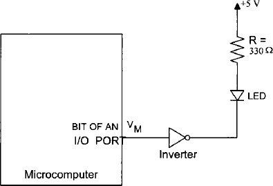
FIGURE 4.2 Microcomputer - LED interface via an inverter

FIGURE 4.3 Seven-segment display.
Seven-segment displays can be interfaced to typical microprocessors using programmed I/O. BCD to seven-segment code converter chips such as 7447 or 7448 can be replaced by a look-up table. This table can be stored in a microcomputer's main memory. An assembly language program can be written to read the appropriate code for a BCD digit stored in this table. This data can be output to display the BCD digit on a seven-segment display connected to an I/O port of the microcomputer. Programs to accomplish this are written in 68000/68020 and Pentium assembly language later in the book.
4.3 Programmed I/O
A microcomputer communicates with an external device via one or more registers called I/O ports using programmed I/O. I/O ports are usually of two types. For one type, each bit in the port can be configured individually as either input or output. For the other type, all bits in the port can be set up as all parallel input or parallel output bits. Each port can be configured as an input or output port by another register called the command or data-direction register. The port contains the actual input or output data. The data-direction register is an output register and can be used to configure the bits in the port as inputs or outputs.
Each bit in the port can be set up as an input or output, normally by writing a 0 or a 1 in the corresponding bit of the data-direction register. As an example, if an 8-bit data-direction register contains 34H (34 Hex), the corresponding port is defined as shown in Figure 4.4. In this example, because 34H (0011 0100) is sent as an output into the data-direction register, bits 0, 1, 3, 6, and 7 of the port are set up as inputs, and bits 2, 4, and 5 of the port are defined as outputs. The microcomputer can then send output to external devices, such as LEDs, connected to bits 2, 4, and 5 through a proper interface. Similarly, the microcomputer can input the status of external devices, such as switches, through bits 0, 1, 3, 6, and 7. To input data from the input switches, the microcomputer inputs the complete byte, including the bits to which LEDs are connected. While receiving input data from an I/O port, however, the microcomputer places a value, probably 0, at the bits configured as outputs and the program must interpret them as “don't cares.” At the same time, the microcomputer's outputs to bits configured as inputs are disabled.

FIGURE 4.4 Bit configurable I/O port along with a data-direction register.

FIGURE 4.5 Parallel I/O ports.
For parallel I/O, there is only one data direction register for all ports. A particular bit in the data direction register configures all bits in the port as either inputs or outputs. Consider two I/O ports in an I/O chip along with one data direction register. Assume that a 0 or a 1 in a particular bit position defines all bits of port A or B as inputs or outputs respectively. An example is depicted in Figure 4.5. Some I/O ports are called handshake ports. Data transfer occurs via these ports through exchanging of control signals between the microcomputer and an external device.
I/O ports are addressed using either standard I/O or memory-mapped I/O techniques. Standard I/O or port I/O (called isolated I/O by Intel) uses an output pin such as the ![]() pin on the Intel Pentium microprocessor chip. The microprocessor outputs a HIGH on this pin to indicate to memory and the I/O chips that a memory operation is taking place. A LOW output from the microprocessor to this pin indicates an I/O operation. Execution of an IN or OUT instruction makes the
pin on the Intel Pentium microprocessor chip. The microprocessor outputs a HIGH on this pin to indicate to memory and the I/O chips that a memory operation is taking place. A LOW output from the microprocessor to this pin indicates an I/O operation. Execution of an IN or OUT instruction makes the ![]() LOW, whereas memory-oriented instructions, such as MOVE, drive the
LOW, whereas memory-oriented instructions, such as MOVE, drive the ![]() to HIGH.
to HIGH.
In standard I/O, the microprocessor uses the ![]() pin to distinguish between I/O and memory. For typical microprocessors, an 8-bit address can be used for each I/O port. With an 8-bit I/O port address, these processors are capable of addressing 256 ports. In addition, 32-bit microprocessors can also use 16- or 32-bit I/O ports.
pin to distinguish between I/O and memory. For typical microprocessors, an 8-bit address can be used for each I/O port. With an 8-bit I/O port address, these processors are capable of addressing 256 ports. In addition, 32-bit microprocessors can also use 16- or 32-bit I/O ports.
In memory-mapped I/O, the microprocessor does not use the ![]() control pin. Instead, the microprocessor uses an unused address pin to distinguish between memory and I/O. The microprocessor uses a portion of the memory addresses to represent I/O ports. The I/O ports are mapped as part of the microprocessor's main memory addresses which may not exist physically, but are used by the microprocessor's memory-oriented instructions, such as MOVE, to generate the necessary control signals to perform I/O. Motorola microprocessors such as the 68000 or 68020 do not have a control pin such as
control pin. Instead, the microprocessor uses an unused address pin to distinguish between memory and I/O. The microprocessor uses a portion of the memory addresses to represent I/O ports. The I/O ports are mapped as part of the microprocessor's main memory addresses which may not exist physically, but are used by the microprocessor's memory-oriented instructions, such as MOVE, to generate the necessary control signals to perform I/O. Motorola microprocessors such as the 68000 or 68020 do not have a control pin such as ![]() and use only memory-mapped I/O. Intel microprocessors can use both types.
and use only memory-mapped I/O. Intel microprocessors can use both types.
When standard I/O is used, typical microprocessors such as the Pentium normally use an IN or OUT instruction with 8-bit ports as follows:
With memory-mapped I/O, the microprocessor normally uses an instruction(i.e., MOV as follows:

4.4 Unconditional and Conditional Programmed I/O
There are typically two ways in which programmed I/O can be utilized: unconditional I/O and conditional I/O. The microprocessor can send data to an external device at any time using unconditional I/O. The external device must always be ready for data transfer. A typical example is that of a microprocessor outputting a 7-bit code through an I/O port to drive a seven-segment display connected to this port. In conditional I/O, the microprocessor outputs data to an external device via handshaking. This means that data transfer occurs via the exchange of control signals between the microprocessor and an external device. The microprocessor inputs the status of the external device to determine whether the device is ready for data transfer. Data transfer takes place when the device is ready. Figure 4.6 illustrates the concept of conditional programmed I/O.

FIGURE 4.6 Flowchart for conditional programmed I/O.
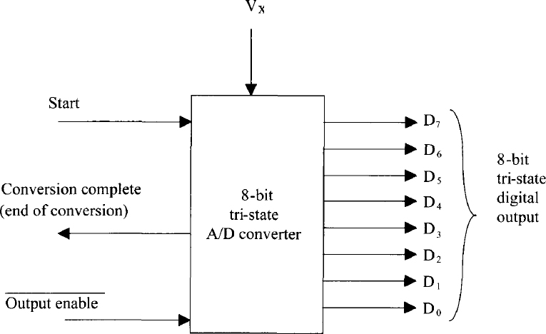
The concept of conditional I/O will now be demonstrated by means of data transfer between a microprocessor and an analog-to-digital (A/D) converter. Consider, for example, the A/D converter shown in Figure 4.7, which transforms an analog voltage Vx into an 8-bit binary output at pins D7-D0. A pulse at the “start” pin initiates the conversion. This drives the “conversion complete” signal LOW. The signal stays LOW during the conversion process. The “conversion complete” signal goes HIGH as soon as the conversion ends. Because the A/D converter's output is tristated, a LOW on the ![]() transfers the converter's outputs. A HIGH on the
transfers the converter's outputs. A HIGH on the ![]() drives the converter's outputs to a high-impedance state.
drives the converter's outputs to a high-impedance state.

FIGURE 4.8 Interfacing an A/D converter to a microcomputer
The concept of conditional I/O can be demonstrated by interfacing an A/D converter to a typical microcomputer. Figure 4.8 shows such an interfacing example. The user writes a program to carry out the conversion process. When this program is executed, the microcomputer sends a pulse to the “start” pin of the converter via bit 2 of port A. The microcomputer then checks the “conversion complete” signal by inputting bit 1 of port A to determine if the conversion is completed.
If the “conversion complete” signal is HIGH (indicating the end of conversion), the microcomputer sends a LOW to the ![]() pin of the A/D converter. The microcomputer then inputs the converter's D0-D7 outputs via port B. If the conversion is not completed, the microcomputer waits in a loop checking for the “conversion complete” signal to go HIGH.
pin of the A/D converter. The microcomputer then inputs the converter's D0-D7 outputs via port B. If the conversion is not completed, the microcomputer waits in a loop checking for the “conversion complete” signal to go HIGH.
4.5 Interrupt I/O
A disadvantage of conditional programmed I/O is that the microcomputer needs to check the status bit (a conversion complete signal of the A/D converter) by waiting in a loop. This type of I/O transfer is dependent on the speed of the external device. For a slow device, this waiting may slow down the microcomputer's ability to process other data. The interrupt I/O technique is efficient in this type of situation.
Interrupt I/O is a device-initiated I/O transfer. The external device is connected to a pin called the interrupt (INT) pin on the microprocessor chip. When the device needs an I/O transfer with the microcomputer, it activates the interrupt pin of the processor chip. The microcomputer usually completes the current instruction and saves the contents of the current program counter and the status register in the stack.
The microcomputer then loads an address automatically into the program counter to branch to a subroutine-like program called the interrupt service routine. This program is written by the user. The external device wants the microcomputer to execute this program to transfer data. The last instruction of the service routine is a RETURN, which is typically similar in concept to the RETURN instruction used at the end of a subroutine. The RETURN from interrupt instruction normally restores the program counter and the status register with the information saved in the stack before going to the service routine. Then the microcomputer continues executing the main program. An example of interrupt I/O is shown in Figure 4.9.
Assume that the microcomputer is 68000 based and is executing the following instruction sequence:


FIGURE 4.9 Microcomputer A/D converter interface via interrupt I/O.
The extensions .B and .W represent byte and word operations. Note that $ and # indicate hexadecimal number and immediate mode respectively. The preceding program is written arbitrarily.
The program logic can be explained using the 68000 instruction set. Ports DDRA and DDRB are assumed to be the data-direction registers for ports A and B, respectively. The first four MOVE instructions configure bits 0 and 7 of port A as outputs and port B as the input port, and then send a trailing “start” pulse (HIGH and then LOW) to the A/D converter along with a HIGH to the ![]() . This HIGH
. This HIGH ![]() is required to disable the A/D's output.
is required to disable the A/D's output.
The microcomputer continues with execution of the CLR.W D0 instruction. Suppose that the “conversion complete” signal becomes HIGH, indicating the end of conversion during execution of the CLR.W D0 instruction. This drives the INT signal to HIGH, interrupting the microcomputer. The microcomputer completes execution of the current instruction, CLR.W D0. It then saves the current contents of the program counter (address BEGIN) and status register automatically and executes a subroutine-like program called the service routine. This program is usually written by the user. The microprocessor manufacturer normally specifies the starting address of the service routine, or it may be provided by the user via external hardware. Assume that this address is $4000 and that the user writes a service routine to input the A/D converter's output as follows:

In this service routine, the microcomputer inputs the A/D converter's output. The return instruction RTE, at the end of the service routine, pops the address BEGIN and the previous status register contents from the stack and loads the program counter and status register with them. The microcomputer executes the MOVE.W D1,D2 instruction at the address BEGIN and continues with the main program. The basic characteristics of interrupt I/O have been discussed so far. The main features of interrupt I/O provided with a typical microcomputer are discussed next.
4.5.1 Interrupt Types
There are typically three types of interrupts: external interrupts, traps or internal interrupts, and software interrupts. External interrupts are initiated through a microprocessor's interrupt pins by external devices such as A/D converters. External interrupts can be divided further into two types: maskable and nonmaskable. Nonmaskable interrupt cannot be enabled or disabled by instructions, whereas a microprocessor's instruction set contains instructions to enable or disable maskable interrupt. For example, the Intel Pentium can disable or enable maskable interrupt by executing instructions such as CLI (clear the interrupt flag in the status register to 0) or STI (set interrupt flag in the status register to 1). The Pentium recognizes maskable interrupt after execution of the STI while ignoring it upon execution of the CLI. Note that the Pentium has an interrupt flag bit in the status register. A nonmaskable interrupt has a higher priority than a maskable interrupt. If maskable and nonmaskable interrupts are activated at the same time, the processor will service the nonmaskable interrupt first.
A nonmaskable interrupt is typically used as a power failure interrupt. Microprocessors normally use +5 V dc, which is transformed from 110 V ac. If the power falls below 90 V ac, the DC voltage of +5 V cannot be maintained. However, it will take a few milliseconds before the ac power drops below 90 V ac. In these few milliseconds, the power-failure-sensing circuitry can interrupt the processor. The interrupt service routine can be written to store critical data in nonvolatile memory such as battery-backed CMOS RAM, and the interrupted program can continue without any loss of data when the power returns.
Some microprocessors, such as the Pentium, are provided with a maskable handshake interrupt. This interrupt is usually implemented by using two pins: INTR and ![]() . When the INTR pin is activated by an external device, the processor completes the current instruction, saves at least the current program counter onto the stack, and generates an interrupt acknowledge
. When the INTR pin is activated by an external device, the processor completes the current instruction, saves at least the current program counter onto the stack, and generates an interrupt acknowledge ![]() . In response to the
. In response to the ![]() , the external device provides an 8-bit number using external hardware on the data bus of the microcomputer. This number is then read and used by the microcomputer to branch to the service routine desired.
, the external device provides an 8-bit number using external hardware on the data bus of the microcomputer. This number is then read and used by the microcomputer to branch to the service routine desired.
Internal interrupts, or traps, are activated internally by exceptional conditions such as overflow, division by zero, or execution of an illegal op-code. Traps are handled in the same way as external interrupts. The user writes a service routine to take corrective measures and provide an indication to inform the user that an exceptional condition has occurred. Many microprocessors include software interrupts, or system calls. When one of these instructions is executed, the microprocessor is interrupted and serviced similarly to external or internal interrupts.
Software interrupt instructions are normally used to call the operating system. These instructions are shorter than subroutine calls, and no calling program is needed to know the operating system's address in memory. Software interrupt instructions allow the user to switch from user to supervisor mode. For some processors, a software interrupt is the only way to call the operating system, because a subroutine call to an address in the operating system is not allowed.
4.5.2 Interrupt Address Vector
The technique used to find the starting address of the service routine (commonly known as the interrupt address vector) varies from one processor to another. With some microprocessors, the manufacturers define the fixed starting address for each interrupt. Other manufacturers use an indirect approach by defining fixed locations where the interrupt address vector is stored.
4.5.3 Saving the Microprocessor Registers
When a microprocessor is interrupted, it normally saves the program counter (PC) and the status register (SR) onto the stack so that the microprocessor can return to the main program with the original values of PC and SR after executing the service routine. The user should know the specific registers the microprocessor saves prior to executing the service routine. This will allow the user to use the appropriate return instruction at the end of the service routine to restore the original conditions upon return to the main program.
4.5.4 Interrupt Priorities
A microprocessor is typically provided with one or more interrupt pins on the chip. Therefore, a special mechanism is necessary to handle interrupts from several devices that share one of these interrupt lines. There are two ways of servicing multiple interrupts: polled and daisy chain techniques.
Polled Interrupts Polled interrupts are handled by software and therefore are slow in servicing the interrupts. The microprocessor responds to an interrupt by executing one general service routine for all devices. The priorities of devices are determined by the order in which the routine polls each device. The microprocessor checks the status of each device in the general service routine, starting with the highest-priority device, to service an interrupt. Once the microprocessor determines the source of the interrupt, it branches to the service routine for the device. Figure 4.10 shows a typical configuration of the polled-interrupt system.
In Figure 4.10, several external devices (device 1, device 2,…, device N) are connected to a single interrupt line of a microprocessor via an OR gate (not shown in the figure). When one or more devices activate the INT line HIGH, the microprocessor pushes the PC and SR onto the stack. It then branches to an address defined by the manufacturer of the microprocessor. The user can write a program at this address to poll each device, starting with the highest-priority device, to find the source of the interrupt. Suppose that the devices in Figure 4.10 are A/D converters. Each converter, along with the associated logic for polling, is shown in Figure 4.11.
Assume that in Figure 4.10 two A/D converters (devices 1 and 2) are provided with the “start” pulse by the microprocessor at nearly the same time. Suppose that the user assigns device 2 the higher priority. The user then sets up this priority mechanism in the general service routine. For example, when the “Conversion complete” signals from device 1 and/or 2 become HIGH, indicating the end of conversion, the processor is interrupted. In response, the microprocessor pushes the PC and SR onto the stack and loads the PC with the interrupt address vector defined by the manufacturer.
The general interrupt service routine written at this address determines the source of the interrupt as follows: A 1 is sent to PA1 for device 2 because this device has higher priority. If this device has generated an interrupt, the output (PB1 ) of the AND gate in Figure 4.11 becomes HIGH, indicating to the microprocessor that device 2 generated the interrupt. If the output of the AND gate is 0, the processor sends a HIGH to PA0 and checks the output (PB0) for HIGH. Once the source of the interrupt is determined, the microprocessor can be programmed to jump to the service routine for that device. The service routine enables the A/D converter and inputs the converter's outputs to the microprocessor.
Polled interrupts are slow, and for a large number of devices the time required to poll each device may exceed the time to service the device. In such a case, a faster mechanism, such as the daisy chain approach, can be used.

Daisy Chain Interrupts Devices are connected in daisy chain fashion, as shown in Figure 4.12, to set up priority systems. Suppose that one or more devices interrupt the processor. In response, the microprocessor pushes the PC and SR onto the stack and, generates an interrupt acknowledge ![]() signal to the highest-priority device (device 1 in this case). If this device has generated the interrupt, it will accept the
signal to the highest-priority device (device 1 in this case). If this device has generated the interrupt, it will accept the ![]() ; otherwise, it will pass the
; otherwise, it will pass the ![]() onto the next device until the
onto the next device until the ![]() is accepted.
is accepted.
Once accepted, the device provides a means for the processor to find the interrupt-address vector by using external hardware. Assume that the devices in Figure 4.12 are A/D converters. Figure 4.13 provides a schematic for each device and the associated logic. Suppose that the microprocessor in Figure 4.12 sends a pulse to start the conversions of the A/D converters of devices 1 and 2 at nearly the same time. When the “conversion complete” signal goes HIGH, the microprocessor is interrupted through the INT line. The microprocessor pushes the PC and SR. It then generates a LOW at the interrupt acknowledge ![]() for the highest-priority device. Device 1 has the highest priority; it is the first device in the daisy chain configuration to receive
for the highest-priority device. Device 1 has the highest priority; it is the first device in the daisy chain configuration to receive ![]() . If A/D converter 1 has generated the “conversion complete” HIGH, the output of the AND gate in Figure 4.13 becomes HIGH.
. If A/D converter 1 has generated the “conversion complete” HIGH, the output of the AND gate in Figure 4.13 becomes HIGH.

FIGURE 4.11 Device N and associated logic for polled interrupt.
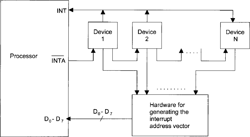
FIGURE 4.12 Daisy chain interrupt.
This signal can be used to enable external hardware to provide the interrupt address vector on the microprocessor's data lines. The microprocessor then branches to the service routine. This program enables the converter and inputs the A/D output to the microprocessor via port B. If A/D converter 1 does not generate the “conversion complete” HIGH, however, the output of the AND gate in Figure 4.13 becomes LOW (an input to device 2's logic) and the same sequence of operations takes place. In the daisy chain, each device has the same logic, with the exception of the last device, which must accept the ![]() . Note that the outputs of all the devices are connected to the INT line via an OR gate (not shown in Figure 4.12).
. Note that the outputs of all the devices are connected to the INT line via an OR gate (not shown in Figure 4.12).

FIGURE 4.13 Each device and the associated logic in a daisy chain.
4.6 Direct Memory Access (DMA)
Direct memory access (DMA) is a technique that transfers data between a microcomputer's memory and an I/O device without involving the microprocessor. DMA is widely used in transferring large blocks of data between a peripheral device such as a hard disk and the microcomputer's memory. The DMA technique uses a DMA controller chip for the data transfer operations. The DMA controller chip implements various components, such as a counter containing the length of data to be transferred in hardware in order to speed up data transfer. The main functions of a typical DMA controller are summarized as follows:
- The I/O devices request DMA operation via the DMA request line of the controller chip.
- The controller chip activates the microprocessor HOLD pin, requesting the microprocessor to release the bus.
- The microprocessor sends HLDA (hold acknowledge) back to the DMA controller, indicating that the bus is disabled. The DMA controller places the current value of its internal registers, such as the address register and counter, on the system bus and sends a DMA acknowledge to the peripheral device. The DMA controller completes the DMA transfer.
There are three basic types of DMA: block transfer, cycle stealing, and interleaved DMA. For block transfer DMA, the DMA controller chip takes over the bus from the microcomputer to transfer data between the microcomputer memory and the I/O device. The microprocessor has no access to the bus until the transfer is completed. During this time, the microprocessor can perform internal operations that do not need the bus. This method is popular with microprocessors. Using this technique, blocks of data can be transferred.
Data transfer between the microcomputer memory and an I/O device occurs on a word-by-word basis with cycle stealing. Typically, the microprocessor is generated by ANDing an ![]() signal with the system clock. The system clock has the same frequency as the microprocessor clock. The DMA controller controls the
signal with the system clock. The system clock has the same frequency as the microprocessor clock. The DMA controller controls the ![]() line. During normal operation, the
line. During normal operation, the ![]() line is HIGH, providing the microprocessor clock. When DMA operation is desired, the controller makes the
line is HIGH, providing the microprocessor clock. When DMA operation is desired, the controller makes the ![]() line LOW for one clock cycle. The microprocessor is then stopped completely for one cycle. Data transfer between the memory and I/O takes place during this cycle. This method is called cycle stealing because the DMA controller takes away or steals a cycle without microprocessor recognition. Data transfer takes place over a period of time.
line LOW for one clock cycle. The microprocessor is then stopped completely for one cycle. Data transfer between the memory and I/O takes place during this cycle. This method is called cycle stealing because the DMA controller takes away or steals a cycle without microprocessor recognition. Data transfer takes place over a period of time.
With interleaved DMA, the DMA controller chip takes over the system bus when the microprocessor is not using it. For example, the microprocessor does not use the bus while incrementing the program counter or performing an ALU operation. The DMA controller chip identifies these cycles and allows transfer of data between memory and the I/O device. Data transfer for this method takes place over a period of time.
Because block transfer DMA is common with microprocessors, a brief description is provided. Figure 4.14 shows a typical diagram of block transfer DMA. In the figure, the I/O device requests DMA transfer via the DMA request line connected to the controller chip. The DMA controller chip then sends a HOLD signal to the microprocessor and waits for the HOLD acknowledge (HLDA) signal from the microprocessor. On receipt of the HLDA, the controller chip sends a DMA ACK signal to the I/O device. The controller takes over the bus and controls data transfer between RAM and the I/O device. On the completion of data transfer, the controller interrupts the microprocessor by the INT line and returns the bus to the microprocessor by disabling the HOLD and DMA ACK signals.
The DMA controller chip usually has at least three registers normally selected by the controller's register select (RS) line: an address register, a terminal count register, and a status register. Both the address and terminal counter registers are initialized by the microprocessor. The address register contains the starting address of the data to be transferred, and the terminal counter register contains the block to be transferred. The status register contains information such as completion of DMA transfer. Note that the DMA controller implements logic associated with data transfer in hardware to speed up the DMA operation.

FIGURE 4.14 Typical block transfer.
4.7 Summary of I/O
Figure 4.15 summarizes various I/O techniques used with a typical microprocessor.

FIGURE 4.15 I/O structure of a typical microcomputer.
Questions and Problems
| 4.1 | Define the three types of I/O. Identify each as either microprocessor-initiated or device-initiated. |
| 4.2 | What is the basic difference between standard I/O and memory-mapped I/O? Identify the programmed I/O technique (s) used by Intel and Motorola microprocessors. |
| 4.3 | What are programmed I/O and virtual I/O? |
| 4.4 | What is the difference between memory mapping in a microprocessor and memory-mapped I/O? |
| 4.5 | Discuss the basic difference between polled I/O and interrupt I/O. |
| 4.6 | What is the difference between subroutine and interrupt I/O? |
| 4.7 | What is an interrupt address vector? |
| 4.8 | Summarize the basic difference between maskable and nonmaskable interrupts. Describe how power failure interrupt is normally handled. |
| 4.9 | Why are polled interrupt and daisy chain interrupt used? |
| 4.10 | Discuss the basic difference between internal and external interrupts. |
| 4.11 | What are cycle stealing, block transfer, and interleaved DMA? |
| 4.12 | Summarize the typical functions performed by a DMA controller chip. |