
APPENDIX F
PENTIUM INSTRUCTION FORMAT AND TIMING
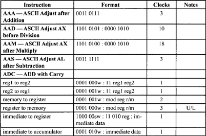
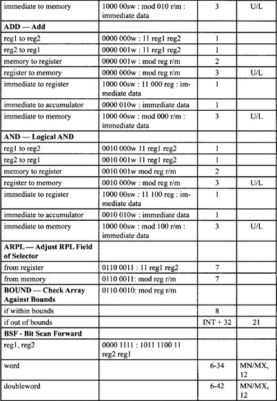
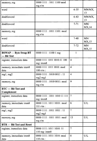
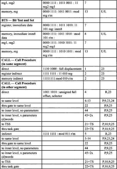
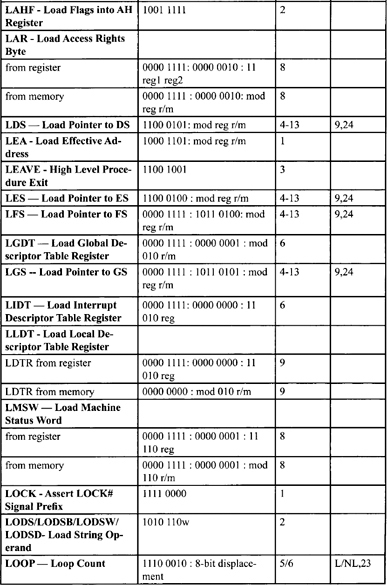
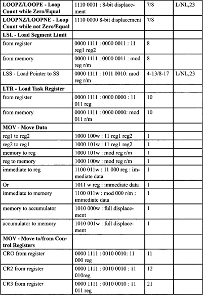
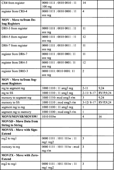
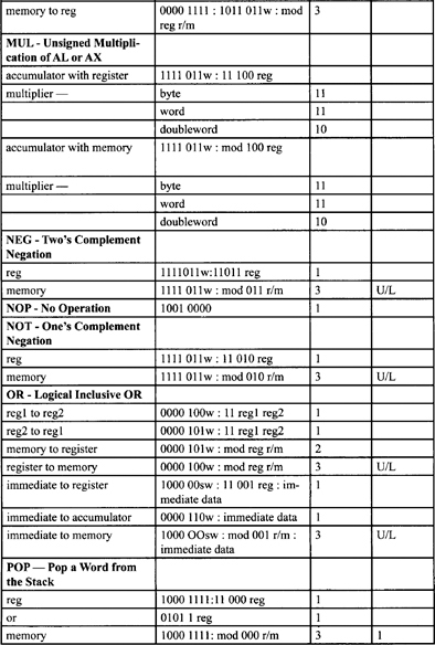
Table F-2, Table F-3, and Table F-5 list all instructions along with instruction encoding diagrams and clock counts.
F.1. INTEGER INSTRUCTION FORMAT AND TIMING
The following sections explain how to use each of the columns of Table F-2.
Format
All instruction encodings are subsets of the general instruction format shown in Figure F-1. Instructions consist of one or two primary opcode bytes, possibly an address specifier consisting of the mod r/m byte and scale-index-base byte, a displacement if required, and an immediate data field if required.
Within the primary opcode or opcodes, smaller encoding fields may be defined. These fields vary according to the class of operation. The fields define such information as direction of the operation, size of displacements, register encoding, or sign extension.
Almost all instructions referring to an operand in memory have an addressing mode byte following the primary opcode byte(s). This byte, the mod r/m byte, specifies the address mode to be used. Certain encodings of the mod r/m byte indicate that a second addressing byte, the scale-index-base byte, follows the mod r/m byte to fully specify the addressing mode.
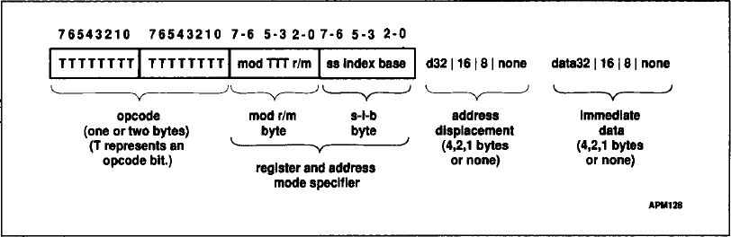
Figure F-1. General Instruction Format
Addressing modes can include a displacement immediately following the mod r/m byte or scale-index-base byte. If a displacement is present, the possible sizes are 8, 16, or 32 bits. If the instruction specifies an immediate operand, the immediate operand follows any displacement bytes. The immediate operand, if specified, is always the last field of the instruction.
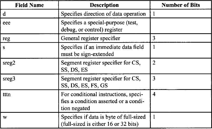
Figure F-1 illustrates several of the fields that can appear in an instruction, such as the mod field and the r/m field, but the figure does not show all fields. Several smaller fields also appear in certain instructions, sometimes within the opcode bytes themselves. Table F-0 is a complete list of all fields appearing in the instruction set. Subsequent tables list the values for each of the fields.
Table F-1. Fields within Instructions
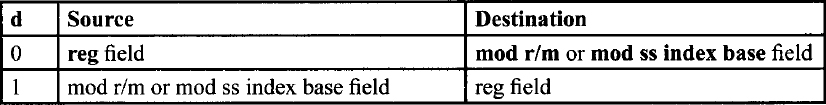
In many two-operand instructions, the d field indicates which operand is considered the source and which is the destination.
Encoding of Operation Direction (d) Field
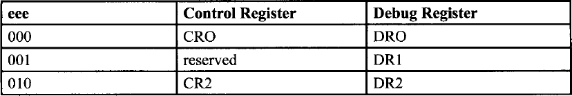
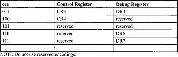
Encoding of Special-Purpose Register (eee) Field
Encoding of reg Field When w Field is Not Present in Instruction
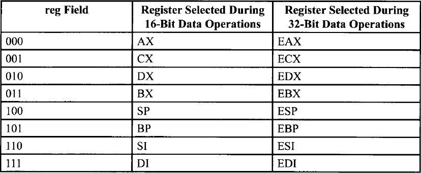
Encoding of reg Field When w Field is Present in Instruction
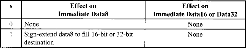
The s field occurs primarily in instructions with immediate data fields. The s field has an effect only if the size of the immediate data is 8 bits and is being placed in a 16-bit or 32-bit destination.
Encoding of Sign-Extend (s) Field
Encoding of the Segment Register (sreg) Field
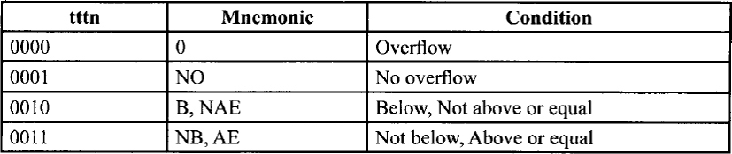
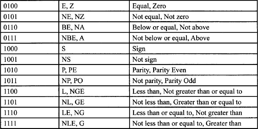
For the conditional instructions (conditional jumps and set on condition), tttn is encoded such that ttt gives the condition to test and n indicates whether to use the condition (n = 0) or its negation (n = 1).
Encoding of Conditional Test (tttn) Field
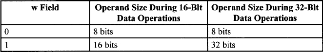
For any given instruction performing a data operation, the instruction is executing as a 32-bit operation or a 16-bit operation. Within the constraints of the operation size, the w field encodes the operand size as either one byte or the full operation size, as shown in the following table.
Encoding of Operand Length (w) Field
Clock Counts
To calculate elapsed time for an instruction, multiply the instruction clock count as listed in the tables by the processor clock period (for example, 15 ns for a 66-MHz processor).
The clock count tables assume that data and instruction access hit their respective caches. A cache miss forces the processor to run an external bus cycle. The 64-bit burst bus of the Pentium processor is defined as r-b-w, where:
r= The number of clocks in the first cycle of a burst read or the number of clocks per data cycle in a nonburst read.
b= The number of clocks for the second and subsequent cycles in a burst read.
w= The number of clocks for a write.
The fastest bus the Pentium processor can support is 2-1-2, assuming zero wait states. The clock counts in the cache miss penalty column assume a 2-1-2 bus. For slower busses, add r — 2 clocks to the cache miss penalty for the first quadword accessed. Other factors also affect instruction clock counts.
To simplify the tables, the following assumptions are made:
1. The external bus is available for reads or writes at all times. Otherwise, add clocks to reads until the bus is available. The processor stalls if the write buffers become full and the external bus is busy. In that case, add clocks to writes until the bus becomes available.
2. If the write buffers become full, subsequent writes are delayed until the write buffers become empty. For the worst case, add w clocks.
3. Accesses are aligned. Add three clocks to each misaligned access.
4. Operands are in the data cache. Add 3 + (number of wait states) for each cache miss.
5. The target of a jump is in the code cache. If not, add r clocks for accessing the destination instruction of a jump. If the destination instruction is not completely contained in the first qword read, add a maximum of 3b clocks. If the destination instruction is not completely contained in the first 32-byte burst, add a maximum of another r + 3b clocks. The penalty for branch misprediction is three clocks.
6. Cache fills complete before subsequent accesses to the same line. If a read misses the cache during a cache fill due to a previous read or prefetch, the read must wait for the cache fill to complete. If a read or write accesses a cache line still being filled, it must wait for the fill to complete.
7. Page translation hits in TLB. A TLB miss typically adds from 13 to 28 clocks to the instruction depending on whether the Accessed or Dirty bit of the page entries needs to be set in memory. This assumes that neither page entry is in the data cache and that a page fault does not occur during address translation.
8. No exceptions are detected during instruction execution. Refer to the Interrupt Clock Counts Table for extra clocks if an interrupt is detected.
9. Instructions that read multiple consecutive data items (for example, task switch, POPA, etc.) and miss the cache are assumed to start the first access on a 32-byte boundary. If not, an extra cache line fill may be necessary, which may add up to r + 3b clocks to the cache miss penalty.
10. No address generation interlocks (AGI). AGIs occur when a register being used as part of an address calculation is the destination register of a previous instruction in either the pipelines. AGIs cause a one clock delay.
The following abbreviations are used in the clock count columns:
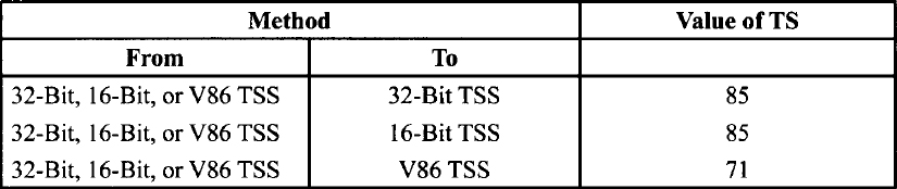
TS The time for a task switch, which depends on the target TSS type as shown in the TaskSwitch Clock Counts Table.
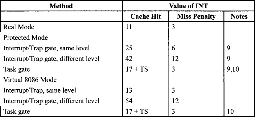
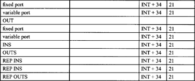
INT The time for an interrupt, which depends on processor mode and type of gate used, as shown in the Interrupt Clock Counts Table.
Task Switch Clock Counts Table
Interrupt Clock Counts Table
Notes
The following abbreviations in the Notes column help to interpret the other columns:
Pairing
The following abbreviations are used in the Pairing column:
| PV | Pairable if issued to V-pipe |
| NP | Not pairable, executes in U-pipe |
| UV | Pairable in either pipe |
| PU | Pairable if issued to U-pipe |
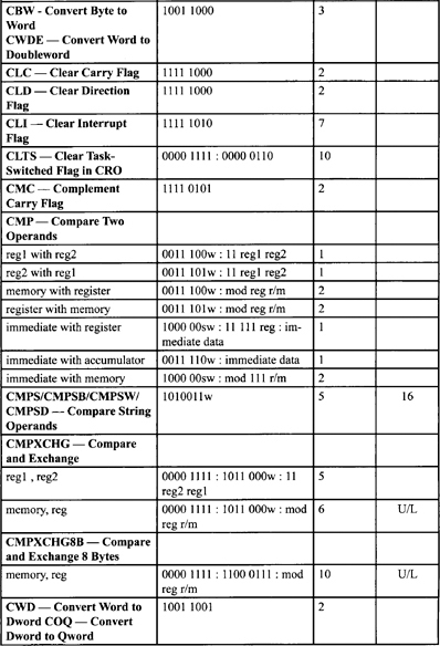
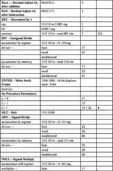
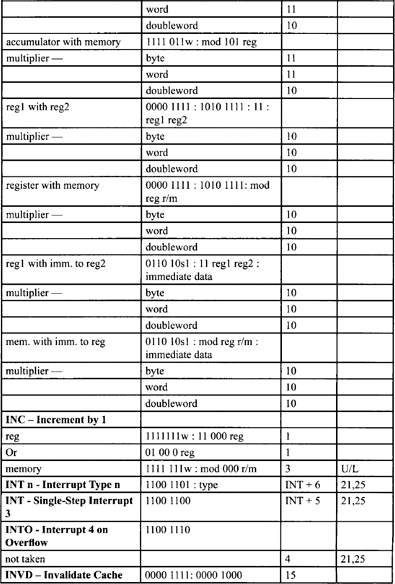
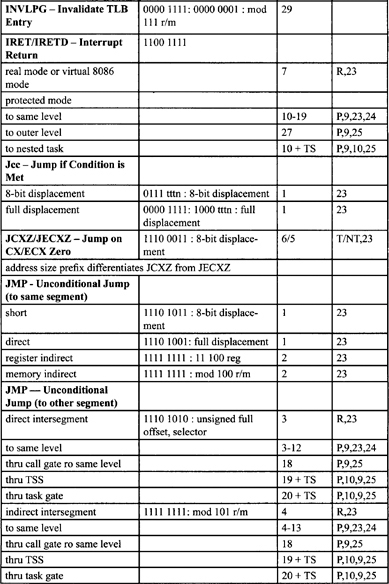
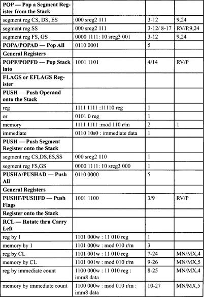
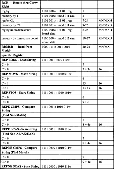
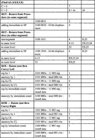
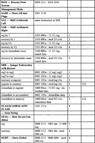
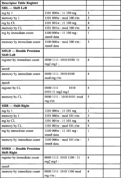
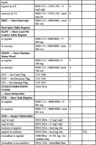
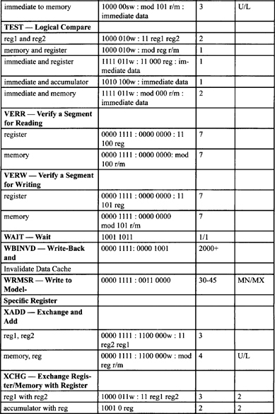
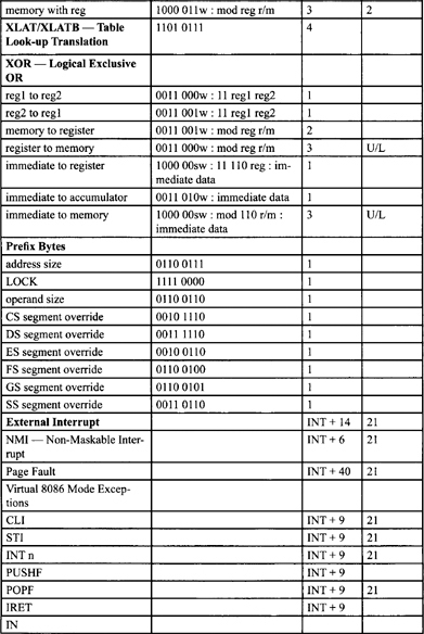
Table F-2. Integer Clock Count Summary
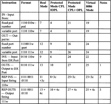
1. Two clock cache miss penalty in all cases.
2. c = count in CX or ECX
3. Cache miss penalty in all modes: Add 2 clocks for every 16 bytes. Entire penalty on second operation.