Squarewave Generator Circuits
Squarewave generators are among the most widely used of all circuits used in modern electronics. They can be used for flashing LED indicators, for generating audio and alarm tones, or, if their leading and trailing edges are really sharp, for ‘clocking’ logic or counter/divider circuitry, etc. Such circuits can be designed to give symmetrical or non-symmetrical outputs, and can be of the free-running or the gated types; in the latter case, they can be designed to turn on with either logic-0 or logic-1 gate signals, and to give either a logic-0 or a logic-1 output when in the OFF mode. The designs can be based on a variety of semiconductor technologies, including the humble transistor, the op-amp, the 555-timer IC, or on CMOS or TTL logic elements, etc. This chapter looks at a variety of designs based on popular TTL and CMOS ICs.
TTL Schmitt Astable Circuits
In TTL applications, the easiest and most cost-effective way to make a squarewave generator is by using a 74LS14 or similar Schmitt inverter element in the basic astable configuration shown in the circuit of Figure 9.1, which operates as follows.
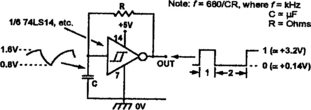
Suppose in Figure 9.1 that C’s voltage has just fallen to the Schmitt’s lower threshold value of 0,8V, making the Schmitt’s output switch to logic-1; under this condition the Schmitt output is at about +3.2V, so C starts to charge exponentially upwards from 0.8V until it reaches the 1.6V upper threshold value of the Schmitt, at which point the Schmitt’s output switches abruptly to a logic-0 value of about 0.14V, and C starts to discharge exponentially downwards from 1.6V until it reaches the 0.8V lower threshold value, at which point the Schmitt’s output switches to logic-1 again, and the whole process repeats again, and so on.
This simple TTL Schmitt astable circuit generates a useful but non-symmetrical squarewave output; its Mark-Space ratio is about 1:2 (i.e. it has a 33% duty cycle), and its operating frequency (f) approximately equals 680/(CR), where C is in µF, R (which can have any value in the 100R to 1k2 range) is in ohms, and f is in kHz; thus, C and R values of 100nF and 1k0 give an operating frequency about 6.8kHz, etc. Note that the operating frequency has a slight positive temperature coefficient, and has a supply voltage coefficient of about +0.5%/100mV The circuit can, in theory, operate at frequencies ranging from below 1Hz (C = 1000µF) to above 10MHz (C = 50pF), but in practice is best limited to the approximate frequency range 400Hz – 2MHz, because the need for large C values makes it uneconomic at low frequencies, and it has poor stability at high frequencies.
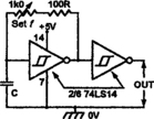
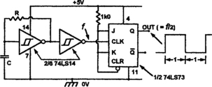
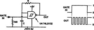
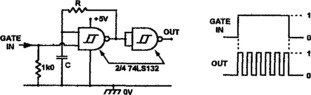
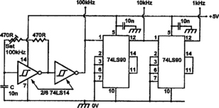
The basic TTL Schmitt astable circuit can be usefully modified in a variety of ways. The operating frequency can, for example, be made variable by using a fixed 100R and variable 1k0 resistor in the R position, and the output waveform can be improved by feeding it through a Schmitt buffer stage, as shown in Figure 9.2. If perfect waveform symmetry is needed, it can be obtained by feeding the output of a buffered Schmitt astable through a JK flip-flop, as shown in Figure 9.3, but note that the final output frequency is half that of the astable. The basic circuit can be converted into a gated Schmitt astable by using a 74LS132 2-input Schmitt NAND gate as its basic element, as shown in Figure 9.4; this particular circuit is gated on by a logic-1 input and has a normally high (logic-1) output; it can be made to give a normally low (logic-0) output by feeding the output through a spare 74LS132 element connected as a simple Schmitt inverter, as shown in Figure 9.5. A major drawback of the TTL Schmitt astable is that its low maximum value of timing resistor (1k2) makes it necessary to use very large values of timing capacitor at low operating frequencies. At 1kHz, for example, timing component values of 1uF and 680R are needed. One alternative way of making a 1kHz TTL squarewave generator is to use a single 10nF capacitor to make a precision 100kHz astable, and then divide its output frequency by 100 via two decade counter ICs, as shown in the circuit of Figure 9.6, which provides outputs of 100kHz, 10kHz, and 1kHz.
CMOS Schmitt Astable Circuits
CMOS Schmitt astables have two major advantages over TTL types. The first is that, because CMOS offers a very high input impedance, they can use large values of timing resistor (up to 10M) and low values of ‘C’ to set a given frequency. The second is that, because CMOS Schmitt elements have reasonably symmetrical upper and lower trigger threshold values, they generate reasonably symmetrical squarewave outputs. Suitable CMOS ICs for use in this type of application are the 40106B Hex Schmitt inverter (see Figure 6.28) and the 4093B Quad 2-input NAND Schmitt trigger (see Figure 6.53). In the latter case, each NAND gate of the 4093B can be used as an inverter by simply disabling one of its input terminals, as shown in the basic Schmitt astable circuit of Figure 9.7.
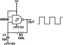
The Schmitt astable circuit gives an excellent performance, with very clean output edges that are unaffected by supply-line ripple and other nasties. The operating frequency is determined by the C1–R1 values, and can be varied from a few cycles per minute to 1MHz or so, the upper limit being determined by the practical limitations of real-life timing resistors and capacitors, etc. The circuit action is such that C1 alternately charges and discharges via R1, without switching the C1 polarity; C1 can thus be a non-polarized component. Note that fast ‘74HC’-series Schmitt elements generate sharper squarewave edges than ‘4000’-series types, but otherwise offer little real advantage over the latter type.
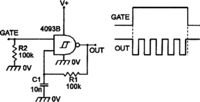
Figure 9.8 shows how the above 4093B-based astable circuit can be modified so that it can be gated on and off via an external signal; the circuit is gated on by a high (logic-1) input, but gives a high output when it is in the gated-off state.
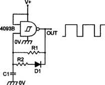
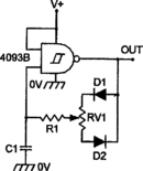
The basic Figure 9.7 astable circuit generates an inherently symmetrical squarewave output. The basic circuit can be made to produce a non-symmetrical output by providing its timing capacitor with alternate charge and discharge paths, as shown in the designs of Figures 9.9 and 9.10. The output M–S ratio of the Figure 9.9 circuit is fixed, but that of the Figure 9.10 circuit can be varied over a wide range via RV1.
2-stage CMOS Astable Basics
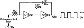
One very popular way to make a CMOS squarewave generator is to wire two CMOS inverter stages in series and use the C–R feedback network shown in the basic 2-stage astable multivibrator circuit of Figure 9.11(a). This circuit generates a good squarewave output from IC1b (and a less-good anti-phase squarewave output from IC1a), and operates at about 1kHz with the component values shown. The circuit operates as follows.
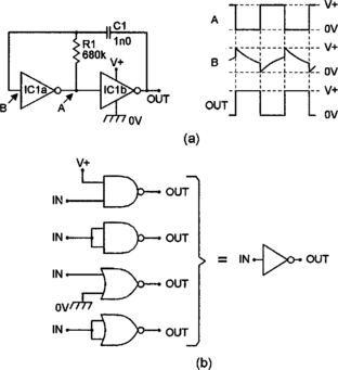
Figure 9.11 (a) Circuit and waveforms of basic 2-stage 1 kHz CMOS astable. (b) Ways of connecting a 2-input NAND or NOR gate as an inverter
In Figure 9.11(a) the two inverters are wired in series, so the output of one goes high when the other goes low, and vice versa. Time-constant network C1–R1 is wired between the outputs of IC1b and IC1a, with the C1–R1 junction fed to the input of the IC1a inverter stage. Suppose initially that C1 is fully discharged, and that the output of IC1b has just switched high (and the output of IC1a has just switched low).
Under this condition, the C1–R1 junction voltage is initially at full positive supply volts, driving the output of IC1a hard low, but this voltage immediately starts to decay exponentially as C1 charges up via R1, until eventually it falls into the linear transfer voltage range of IC1a, making its output start to swing high. This swing is amplified by inverter IC1b, initiating a regenerative action in which IC1b output switches abruptly to the low state (and IC1a output switches high). This switching action makes the charge of C1 try to apply a negative voltage to the input of IC1a, but the built-in protection diodes of IC1a prevent this, and instead discharge C1.
Thus, at the start of the second cycle, C1 is again fully discharged, so in this case the C1–R1 junction is initially at zero volts (driving IC1a output high), but the voltage then rises exponentially as C1 charges up via R1, until eventually it rises into the linear transfer voltage range of IC1a, thus initiating another regenerative switching action in which IC1b output switches high again (and IC1a output switches low), and C1 is initially discharged via the IC1a input protection diodes. The operating cycle then continues ad infinitum.
The operating frequency of the above circuit is inversely proportional to the C–R time constant (the period is roughly 1.4CR), so can be raised by lowering the values of C1 or R1. C1 must be a non-polarized capacitor and can have any value from a few tens of pF to several µF, and R1 can have any value from about 4k7 to 22M; the astable operating frequency can vary from a fraction of a Hz to about 1MHz. For variable-frequency operation, wire a fixed and a variable resistor in series in the R1 position.
In practice, each of the circuit’s inverter stages can be made from a single gate of a 4001B Quad 2-input NOR gate or a 4011B Quad 2-input NAND gate, etc., by using the connections shown in Figure 9.11(b); the inputs of all unused gates in these ICs must be tied to one or other of the supply line terminals. The Figure 9.11(a) astable can (like all other CMOS astable circuits shown in this chapter) use any supplies in the range 3V to 15V if based on a ‘4000’-series IC such as the 4001B or 4011B, etc., or 2V to 6V if based on a ‘74HC’-series device.
The output of the Figure 9.11(a) astable switches (when lightly loaded) almost fully between the zero and positive supply-rail values, but the C1–R1 junction voltage is prevented from swinging below zero or above the positive supply-rail levels by the built-in clamping diodes at the input of IC1a. This factor makes the operating frequency somewhat dependent on supply-rail voltages. Typically, the frequency falls by about 0.8% for a 10% rise in supply voltage; if the frequency is normalized with a 10V supply, the frequency falls by 4% at 15 V or rises by 8% at 5 V.
The operating frequency of the Figure 9.11(a) circuit is also influenced by the transfer voltage value of the individual IC1a inverter/gate that is used in the astable, and can be expected to vary by as much as 10% between different ICs. The output symmetry of the ‘square’ waveform also depends on the transfer voltage value, and in most cases the circuit will give a non-symmetrical output. In most non-precision and hobby applications these defects are, however, of little practical importance.
2-stage Astable Variations
Some of the defects of the Figure 9.11(a) circuit can be minimized by using the ‘compensated’ astable of Figure 9.12, in which R2 is wired in series with the input of IC1a. This resistor must have a value that is large relative to R1, and its main purpose is to allow the C1–R1 junction to swing freely below the zero and above the positive supply-rail voltages during the astable operation and thus improve the frequency stability of the circuit. Typically, when R2 is ten times the value of R1, the frequency varies by only 0.5% when the supply voltage is varied between 5 and 15 volts. An incidental benefit of R2 is that it gives a slight improvement in the symmetry of the astable output waveform.
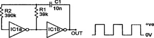
The basic and compensated astable circuits of Figures 9.11 and 9.12 can be built with several detail variations, as shown in Figures 9.13 to 9.17. In the basic astable circuit, for example, C1 alternately charges and discharges via R1 and thus has a fixed symmetry. Figures 9.13 to 9.15 show how the basic circuit can be modified to give alternate C1 charge and discharge paths and thus to allow the symmetry to be varied at will.
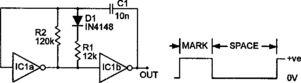
Figure 9.13 Modifying the astable to give a non-symmetrical output: MARK is controlled by the parallel values of R1 and R2: SPACE is controlled by R2 only
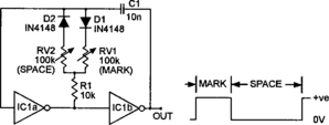
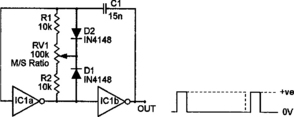
Figure 9.15 The MARK-SPACE ratio of this astable is fully variable from 1:11 to 11:1 via RV1; frequency is almost constant at about 1 kHz
The Figure 9.13 circuit generates a highly non-symmetrical waveform, equivalent to a fixed pulse delivered at a fixed timebase rate. Here, C1 charges in one direction via R2 in parallel with the D1–R1 combination, to generate the MARK or pulse part of the waveform, but discharges in the reverse direction via R2 only, to give the SPACE between the pulses. The Figure 9.14 circuit, however, generates a waveform with independently variable MARK and SPACE times; the MARK is controlled by R1-RV1-D1, and the SPACE by R1-RV2-D2. Finally, the Figure 9.15 circuit generates a variable symmetry or M–S ratio output while maintaining a near-constant frequency; here, C1 charges in one direction via D2 and the lower half of RV1 and R2, and in the other direction via D1 and the upper half of RV1 and R1, and the M–S ratio can be varied over the range 1:11 to 11:1 via RV1.
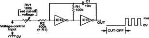
Figures 9.16 and 9.17 show ways of using the basic 2-stage astable circuit as a very simple VCO. The Figure 9.16 circuit can be used to vary the operating frequency over a limited range via an external voltage. R2 must be at least twice as large as R1 for satisfactory operation, the actual value depending on the required frequency-shift range: a low R2 value gives a large shift range, and a large R2 value gives a small shift range. The Figure 9.17 circuit acts as a special-effects VCO in which the oscillator frequency rises with input voltage, but switches off completely when the input voltage falls below a value preset by RV1.
Gated 2-stage Astable Circuits
All of the 2-stage CMOS astable circuits of Figures 9.11 to 9.15 can be modified for gated operation, so that they can be turned on and off via an external signal, by simply using a 2-input NAND (4011B, etc.) or NOR (4001B, etc.) gate in place of the inverter in the IC1a position and by applying the input gate control signal to one of the gate input terminals. Note, however, that the NAND and the NOR elements give quite different types of gate control and output operation in these applications, as shown by the two basic versions of the gated astable in Figures 9.18 and 9.19.
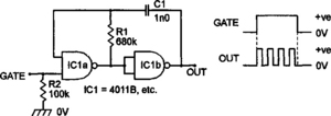
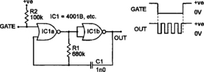
Figure 9.19 This version of the gated astable has a normally high output and is gated on by a low (logic-0) input
Note specifically from these two circuits that the NAND version is gated on by a logic-1 input and has a normally low output, while the NOR version is gated on by a logic-0 input and has a normally high output. R2 can be eliminated from these circuits if the gate drive is direct-coupled from the output of a preceding CMOS logic stage, etc. Also note in these gated astable circuits that the output signal terminates as soon as the gate drive is removed; consequently, any noise present at the gate terminal also appears at the outputs of these circuits. Figures 9.20 and 9.21 show how to modify the circuits so that they produce ‘noiseless’ outputs.
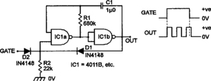
Figure 9.20 Semi-latching or ‘noiseless’ gated astable circuit, with logic-1 gate input and normally zero output
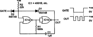
Figure 9.21 Alternative semi-latching gated astable, with logic-0 gate input and normally high output
Here, the gate signal of IC1a is derived from both the outside world and from the output of IC1b via diode OR gate D1–D2–R2. As soon as the circuit is gated from the outside world via D2 the output of IC1b reinforces or self-latches the gating via D1 for the duration of one half astable cycle, thus eliminating any effects of a noisy outside world signal. The outputs of these semi-latching gated 2-stage astable circuits are thus always complete numbers of half cycles.
CMOS Ring-of-three Astable
The CMOS 2-stage astable circuit is a good general-purpose squarewave generator, but is not always suitable for direct use as a ‘clock’ generator with fast-acting counting and dividing circuits, since it tends to pick up and amplify any existing supply line noise during the ‘transitioning’ parts of its operating cycle and thus to produce output squarewaves with ‘glitchy’ leading and trailing edges. A far better type of clock generator circuit is the ring-of-three astable shown in Figure 9.22.

The Figure 9.22 ring-of-three circuit is similar to the basic 2-stage astable, except that its input stage (IC1a-IC1b) acts as an ultra-high-gain non-inverting amplifier and its main timing components (C-R1) are transposed (relative to the 2-stage astable). Because of the very high overall gain of the circuit, it produces an excellent and glitch-free squarewave output that is ideal for clock generator use.
The basic ring-of-three astable can be subjected to all the design modifications already described for the basic 2-stage astable, e.g. it can be used in either basic or compensated form and can give either a symmetrical or non-symmetrical output, etc. The most interesting variations of the circuit occur, however, when it is used in the gated mode, since it can be gated via either the IC1b or IC1c stages. Figures 9.23 to 9.26 show four variations on this gating theme.
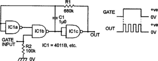
Figure 9.23 This gated ring-of-three astable is gated by a logic-1 input and has a normally low output
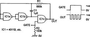
Figure 9.24 This gated ring-of-three astable is gated by a logic-1 input and has a normally high output
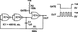
Figure 9.25 This gated ring-of-three astable is gated by a logic-0 input and has a normally low output
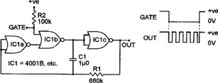
Figure 9.26 This gated ring-of-three astable is gated by a logic-0 input and has a normally-high output
Thus, the Figure 9.23 and 9.24 circuits are both gated on by a logic-1 input signal, but the Figure 9.23 circuit has a normally low output, while that of Figure 9.24 is normally high. Similarly, the Figure 9.25 and 9.26 circuits are both gated on by a logic-0 signal, but the output of the Figure 9.25 circuit is normally low, while that of Figure 9.26 is normally high.
CMOS 555 IC Circuits
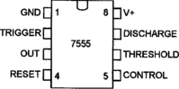
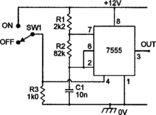
Most readers will know that the popular 555 timer IC can be wired in the astable mode and used to generate excellent squarewave output signals, and that a CMOS version of this device is also available and is known as the ICM7555 or – more commonly – as the ‘7555’. Figure 9.27 shows the outline of this CMOS IC, and Figure 9.28 shows it wired in the basic astable mode.

The action of the Figure 9.28 basic 7555 astable is such that C1 alternately charges via R1–R2 and discharges via R2 only, generating an excellent near-symmetrical squarewave output that is suitable for use as a clock waveform. Note that R2 acts as the main time-constant resistor, and can have any value from about 4k0 to 22M, and C1 is the time-constant capacitor, and can have any value from a few pF to many hundreds of µF, and may be of the polarized or non-polarized types.
The 7555 astable circuit can only work if pin-4 is tied to the positive supply rail; if pin-4 is grounded, the astable is disabled. The astable can thus be used in the gated mode by simply wiring pin-4 as shown in Figure 9.29.
The basic 7555 astable circuit generates an almost symmetrical output waveform. It can be made to generate a non-symmetrical waveform in a variety of ways. Figure 9.30 shows one useful variation. In this case C1 alternately charges via R1–R3 and D2, and discharges via D1–RV1 and R2; the output waveform symmetry of this circuit is thus fully variable via RV1.

4046B VCO Circuits
Another popular ‘CMOS’ way of generating good squarewaves is via the VCO (voltage-controlled oscillator) section of the 4046B phase-locked-loop (PLL) IC (or its 74HC-series equivalent, the 74HC4046). Figure 9.31 shows the internal block diagram and pin-outs of this excellent IC, which contains a couple of phase comparators, a VCO, a zener diode, and a few other bits and pieces.
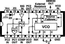
Figure 9.31 Internal block diagram and pin-outs of the 4046B (and its ‘HC’ equivalent, the 74HC4046)
For present purposes, the most important part of the IC is the VCO section. This is a highly versatile element. It produces a well-shaped symmetrical squarewave output, has a top-end frequency limit in excess of 1MHz (15MHz in the 74HC4046), has a voltage-to-frequency linearity of about 1% and can easily be scanned through a 1 000 000:1 range by an external voltage applied to the VCO input terminal. The frequency of the oscillator is governed by the value of a capacitor (minimum value 50pF) connected between pins 6 and 7, by the value of a resistor (minimum value 10k) wired between pin-11 and ground, and by the voltage (any value from zero to the supply voltage value) applied to VCO input pin-9.
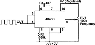
Figure 9.32 shows the simplest possible way of using the 4046B VCO as a voltage-controlled squarewave generator. Here, C1–R1 determine the maximum frequency that can be obtained (with the pin-9 voltage at maximum) and RV1 controls the actual frequency by applying a control voltage to pin-9; the frequency falls to a very low value (a fraction of a Hz) with pin-9 at zero volts. The effective voltage-control range of pin-9 varies from roughly 1V0 below the supply value to about 1V0 above zero, and gives a frequency span of about 1 000 000:1. Ideally, the circuit’s supply voltage should be regulated.
It is stated above that the frequency falls to near-zero when the input voltage of the Figure 9.32 circuit is reduced to zero. Figure 9.33 shows how the circuit can be modified so that the frequency falls all the way to zero with zero input, by wiring high-value resistor R2 between pins 12 and 16. Note here that, when the frequency is reduced to zero, the VCO output randomly settles in either a logic-0 or a logic-1 state. Figure 9.34 shows how the pin-12 resistor can alternatively be used to determine the minimum operating frequency of a restricted-range VCO. Here, fmin is determined by C1–R2, and fmax is determined by C1 and the parallel resistance of R1 and R2.
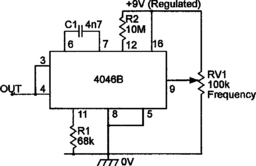
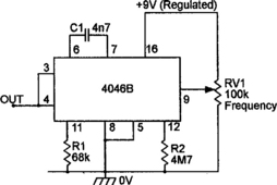
Figure 9.35 shows an alternative version of the restricted-range VCO, in which fmax is controlled by C1–R1, and fmin is determined by C1 and the series combination of R1 and R2. Note that, by suitable choice of the R1 and R2 values, the circuit can be made to span any desired frequency range from 1:1 to near infinity.
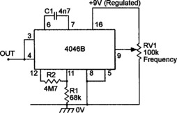
Figure 9.35 Alternative version of the restricted-range VCO. fmax is controlled by C1–R1, fmin by C1 – (R1 + R2)
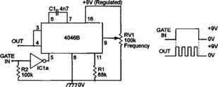
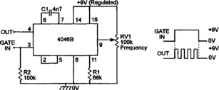
Finally, it should be noted that the VCO section of the 4046B can be disabled by taking pin-5 of the package high (to logic-1) or enabled by taking pin-5 low (to logic-0). This feature makes it possible to gate the VCO on and off via external signals. Thus, Figure 9.36 shows how the basic VCO circuit can be gated via a signal applied to an external inverter stage. Alternatively, Figure 9.37 shows how one of the internal phase comparators of the 4046B can be used to provide gate inversion, so that the VCO can be gated via an external voltage applied to pin-3.
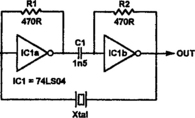
A TTL Crystal Oscillator
To complete this look at squarewave generator circuits, Figure 9.38 shows how two simple 74LS04 or similar TTL inverter elements can be used as the basis of a crystal oscillator by biasing them into their linear modes via 470R feedback resistors and then AC coupling them in series via C1, to give zero overall phase shift; the circuit is then made to oscillate by wiring the crystal (which must be a series resonant type) between the output and input as shown. This circuit can operate from a few hundred kHz to above 10MHz.