Special-purpose ICs and Circuits
So far, this Volume has dealt with mainly run-of-the mill digital ICs such as logic gates, bilateral switches, flip-flops, counters, latches, and other devices of the type that the average professional digital circuit designer is likely to use on a regular basis. But there are other useful types of digital IC that may be needed only very rarely, and among them are dedicated multiplexers, decoders and demultiplexers, addressable latches, full-adders, and bus transceivers. This chapter explains how to use these types of special-purpose ICs, and concludes by giving functional descriptions of a few other unusual and very rarely used types of logic IC.
Multiplexing Basics
Multiplexers and demultiplexers were briefly defined in Chapter 7, where it was explained that some CMOS bilateral switch ICs are designed for use as versatile multi-channel multiplexer/demultiplexer units. Several ‘74LS’-series TTL ICs and a few ‘74HC’-series CMOS types are, however, designed purely as dedicated multiplexers or as dedicated demultiplexer devices, and some of these ICs are described in the next two sections of this chapter.
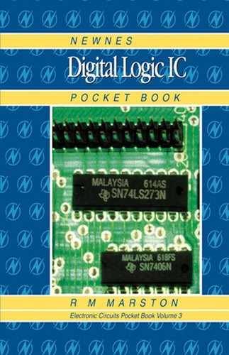
A multiplexer is a device that enables two or more signals to be selected and combined into a single output that can subsequently be demultiplexed in a way that enables the original signals to be retrieved. Figure 14.1 illustrates the basic principle of a multiplexing system. Imagine here that the two switches are motor driven and continuously rotate and are somehow remotely ganged so that SW2 is in position ‘1’ when SW1 is in position ‘1’, and so on; consequently, the 4-bit data from the four input lines is repeatedly sequentially inspected via SW1 and converted into serial form (multiplexed), and then shoved down the data link to SW2, where it is demultiplexed and reappears in its original 4-bit form on four separate output lines. The big feature of this system is, of course, that it enables a whole stack of parallel data to be transmitted – in serial form – via a single data link such as an electric or fibre-optic cable or a wireless carrier wave, etc.

Figure 14.2 shows, in greatly simplified form, an electronic version of the above circuit. Here, at the transmitter end of the system, SW1 is replaced by a 4-input multiplexer, the action of which is such that any of the four data input lines can be coupled to the OUT line by applying a suitable 2-bit binary address code (00, 01, 10, or 11). These codes are generated sequentially by the divide-by-4 counter (consisting of two cascaded divide-by-2 flip-flops), which is driven by a clock-pulse generator that produces narrow trigger pulses. The outputs of the multiplexer and the clock-pulse generator are mixed together in the 2-input AND gate and transmitted down the single data link; at the receiver end of the system, the clock pulses are extracted from the data link and used to drive another divide-by-4 counter that generates address codes for the 1-line to 4-line demultiplexer, which reconstructs the original input data and puts it out on four separate lines.
The above circuit is, of course, greatly simplified, and in practice would need the addition of a pulse synchronization system and a few other refinements to make it work properly, but it does serve to illustrate the basic multiplexing principle. Note in particular that multiplexers and demultiplexers are really meant to form individual elements in a highly specialized type of system, but that in practice a multiplexer actually functions as an addressable data selector (like SW1 in Figure 14.1), and a demultiplexer functions as an addressable data distributor (like SW2 in Figure 14.1) or as a binary-code ‘decoder’, and in these modes both types of device are so useful that they are usually described as ‘multiplexer/data-selector’ and ‘demultiplexer/decoder’ ICs.
Note in Figure 14.1 that SW1 and SW2 can both pass signals in either direction, and can thus be used as either multiplexers or demultiplexers by simply placing them in the appropriate part of the system. In practice, however, dedicated multiplexers and demultiplexers can only pass signals in a single direction.
Popular Multiplexer ICs
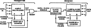
The three best known types of current-production TTL multiplexer IC are the 74LS157 Quad 2-input IC, the 74LS153 Dual 4-input IC, and the 74LS151 8-input IC, which are also available in similarly numbered ‘74HC’-series fast CMOS versions. Figure 14.3 shows the functional diagram of the 74LS157 (or 74HC157), which effectively houses four ganged 2-way (’A’ or ‘B’) switches with buffered outputs that can be disabled (driven low) by biasing INH pin-15 high; the switch positions can be selected via pin-1, which selects position ‘A’ when biased low or ‘B’ when biased high. The 74LS157 is very easy to use, and Figure 14.4 shows how to connect it as a data-selector that can select either of two 4-bit input words via pin-1. This circuit is useful in applications where, for example, either of two 4-bit codes needs to be sent to the PRESET terminal of a counter/divider IC, etc.

Figure 14.3 Functional diagram of the 74LS157 (or 47HC157) Quad 2-input data-selector/multiplexer IC
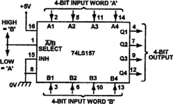
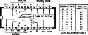
Figure 14.5 shows the functional diagram of the 74LS153 (or 74HC153), which effectively houses two ganged 4-way (A to D) switches with buffered outputs that can be disabled (driven low) by biasing the appropriate INH terminal (pins 1 or 15) high; the switch positions can be selected by applying the appropriate BA binary codes to pins 2 and 14, as indicated in the Figure 14.5 table. Figure 14.6 shows how to connect the IC as a Dual 4-way input selector, in which each ‘switch’ outputs the input data that is selected via the BA ‘select’ code. Note that the IC can be used as a Dual 2-bit decoder by applying the 2-bit code to the BA terminals and tying all but one of each switch’s four inputs low, so that the switch’s output goes high only when the desired 2-bit code is present, as indicated in the IC’s Data Selection Table; thus, the ‘10’ BA code can be detected by tying only the ‘C’ input high, etc.
Figure 14.5 Functional diagram and Data Selection Table of the 74LS153 (or 74HC153) Dual 4-input data selector/multiplexer IC
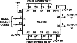
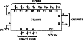
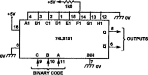
Figure 14.7 shows the functional diagram of the 74LS151 (or 74HC151), which effectively houses a single 8-way (’A1’ to ‘H1’) switch with a buffered output that can be disabled (driven low) by biasing the INH terminal high; the switch positions can be selected by applying the appropriate CBA 3-bit binary codes to pins 9–10–11, as indicated in the Figure 14.7 table. Figure 14.8 shows how to connect the IC as an 8-way input selector, which outputs whichever switch input is selected via the CBA ‘select’ code; a direct output is available on pin-5, and an inverted one on pin-6. Alternatively, Figure 14.9 shows the IC wired as a 3-bit decoder, with the 3-bit code applied to the CBA terminals and with all but one of the eight inputs tied low, so that the pin-5 output goes high only when the desired 3-bit code is present (see the Figure 14.7 Data Selection Table); the IC is shown connected to detect the ‘101’ code, which selects the F1 input, which in this case is tied high.
Popular Demultiplexer ICs
The three best known types of current-production TTL decoder/demultiplexer ICs are the 74LS139 Dual 4-output IC, the 74LS138 8-output IC, and the 74LS154 16-output IC, which all have active-low outputs and are also available in similarly numbered ‘74HC’-series versions. Figure 14.10 shows the functional diagram of the 74LS139 (or 74HC139), which effectively houses two independent 4-way (NOT-A to NOT-D) selectors with active-low buffered outputs that can all be disabled (driven high) by biasing the INH terminal high; the switch positions are selected via a 2-bit BA binary code, as shown in the diagram’s Decoding Table. The 74LS139 can be used as a Dual 2-bit 4-way (2-line to 4-line) decoder by connecting it as shown in Figure 14.11, with the INH terminals grounded and the decoded outputs taken from the appropriate output terminals (see the IC’s Decoding Table); thus, the NOT-C output is normally high, and goes low only in the presence of a ‘10’ BA input code, etc. The IC can be used as a demultiplexer by using the INH terminal as the data input.
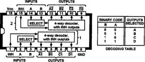
Figure 14.10 Functional diagram and Decoding Table of the 74LS139 (or 74HC139) Dual 4-way decoder/demultiplexer IC
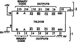
Figure 14.11 Normal connections for using the 74LS139 (or 74HC139) as a Dual 2-line to 4-line decoder
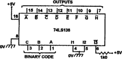
Figure 14.12 shows the functional diagram and Decoding Table of the 74LS138 (or 74HC138), which effectively houses an 8-way selector with active-low buffered outputs that can all be disabled (driven high) by biasing the I1 or I2 INH terminal high or the NOT-I3 terminal low; the switch positions are selected via a 3-bit CBA binary code, as shown in the diagram’s Decoding Table. The 74LS138 can be used as a 3-bit 8-way (3-line to 8-line) decoder by connecting it as shown in Figure 14.13, with the decoded outputs taken from the appropriate output terminals (see the IC’s Decoding Table); each output is normally high, but goes low when activated by its 3-bit ‘select’ code. This IC can be used as a demultiplexer by using one of the active-low INH terminals as the data input, with the other two INH inputs disabled.

Figure 14.12 Functional diagram and Decoding Table of the 74LS138 (or 74HC138) 8-way decoder/demultiplexer IC
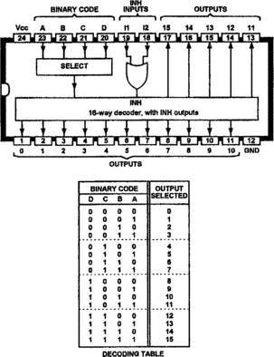
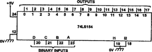
Finally, Figure 14.14 shows the functional diagram and Decoding Table of the 24-pin 74LS154 (or 74HC154), which effectively houses a 16-way selector with active-low buffered outputs that can all be disabled (driven high) by biasing either of the two INH terminals high; the switch positions are selected via a 4-bit DCBA binary code, as shown in the Decoding Table. The 74LS154 can be used as a 4-bit 16-way (4-line to 16-line) decoder by connecting it as in Figure 14.15, with the decoded outputs taken from the appropriate output terminals (see the IC’s Decoding Table); each output is normally high, but goes low when activated by its 4-bit ‘select’ code. The IC can be used as a demultiplexer by tying one INH input low and using the other INH terminal as a data input.
Addressable Latches
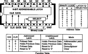
Chapter 13 gives a reasonably full description of conventional data latch ICs, in which groups of latch elements are ganged together and activated by a single clock signal. An ‘addressable latch’ IC, on the other hand, is a special unit in which a single clock signal and data input, etc., can be ‘addressed’ (applied) to individual latch elements among a group, one at a time; the ‘address’ takes the form of a binary code (2-bits for four latches, 3-bits for eight latches). The best known TTL IC of this type is the 74LS259 8-bit addressable latch, which is also available in a fast CMOS version as the 74HC259; Figure 14.16 shows the functional diagram, Address Table, and Function Table of the 74LS259 (or 74HC259). This IC has four basic operating modes (see the Function Table), as follows:

Figure 14.16 Functional diagram, Address Table, and Function Table of the 74LS259 (or 74HC259) 8-bit addressable latch IC
1. When NOT-CLR is low and CLK is high, all latches are cleared and the QO to Q7 outputs go low.
2. When NOT-CLR and CLK are low, the IC acts as a 3-line to 8-line decoder (or as a demultiplexer) in which the selected output is active-high and all other outputs are low.
3. When NOT-CLR is high and CLK is low, the IC acts as an addressable transparent latch, in which the Q output of the selected latch follows the data input, and all other latches remain in their previous states.
4. When NOT-CLR and CLK are high, the current data is latched into the selected latch.
The 74LS/HC259 is thus a reasonably versatile unit that can be used as an 8-bit serial-in to parallel-out converter, as a general-purpose memory unit, or as a decoder or demultiplexer, etc. Figure 14.17 shows it used as a 3-line to 8-line decoder that drives the selected output high in the presence of the correct address code, and Figure 14.18 shows it used as an 8-bit demultiplexer, with the serial input applied to the data terminal and the clock signal (which would also drive the 3-stage counter that generates the CBA binary ‘select’ code) applied to the CLK terminal.
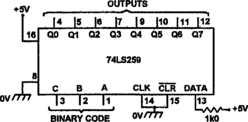
Figure 14.17 Connections for using the 74LS259 (or 74HC259) as a 3-line to 8-line decoder with active-high outputs

Figure 14.19 shows the functional diagram, Address Table, and Function Table of a popular CMOS 8-bit addressable latch IC, the 4099B. In this IC, the DIS (select DISABLE) input acts a bit like a clock terminal, and must be pulled low (to logic-0) to load the binary select code into the latches. When DIS is pulled low, the IC acts as an addressable latch when CLR is low, or as a demultiplexer when CLR is high. When DIS is biased high, the IC acts as an 8-bit memory when CLR is low, and all latches are reset (with their ‘Q’ outputs set low) when CLR is high.
Full-adder ICs
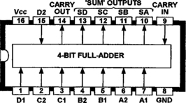
The basic principles of binary half-adder and full-adder circuits are outlined in Chapter 6. The two best known TTL ICs of the latter type are the 74LS83 and the 74LS283 4-bit full-adders, which are functionally identical but have different pin-outs, as shown in Figures 14.20 and 14.21. Each of these ICs generates a 4-bit plus CARRY output equal to the sum (’S’) of two 4-bit (DCBA) input words (’1’ and ‘2’); numbers of these ICs can be coupled together to carry out binary addition on words of any desired bit size.


Figure 14.22 shows the basic way of using the 74LS83 or 74LS283 as a single 4-bit adder; the CARRY IN terminal is tied low, word ‘1’ is applied to one set of input terminals and word ‘2’ is applied to the other, and the result of the addition appears on the ‘S’ output terminals. If the result of the addition is greater than decimal 15 (binary 1111), the CARRY OUT terminal goes to logic-1, and thus acts as a bit-5 output.
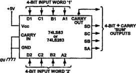
Figure 14.23 shows how to interconnect two 4-bit full-adders to make an 8-bit adder. The least-significant four bits of each input word are applied to IC1, which has its CARRY IN terminal tied low, and the four most-significant bits are applied to IC2, which has its CARRY IN terminal tied to the CARRY OUT of IC1. IC1 provides the four least-significant bits of the resulting sum, and IC2 provides the four most-significant bits plus a CARRY OUT, which acts as bit-9. This basic circuit can be expanded upwards to accept input words of any desired bit size by taking the CARRY OUT of each successive lower-order stage to the CARRY IN terminal of the next higher-order stage in the chain.

The two best known CMOS 4-bit full-adder ICs are the 74HC283, which is a fast CMOS version of the 74LS283, and the 4008B, which has the functional diagram shown in Figure 14.24. These two ICs are used in exactly the same way as already shown in Figures 14.22 and 14.23.
Bus Transceiver ICs
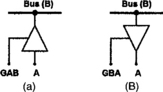
In digital electronics, ‘bus driver’ and ‘bus receiver’ elements are simply high fan-out buffers or inverters with 3-state outputs, and can be used to either make or break a circuit’s input or output contact with a common bus line. Figure 14.25 illustrates the basic principle, using non-inverting buffers. Thus, in (a), the element acts as a bus driver and allows point ‘A’ to communicate with ‘B’ (the bus line) when terminal GAB is high, but is put into the high-impedance 3-state mode when GAB is low. In (b), the element acts as a bus receiver and allows the bus (B) to communicate with point ‘A’ when GBA is high, but isolates the two points when GBA is low.
A ‘bus transceiver’ circuit simply consists of a bus driver and bus receiver element wired in inverse parallel, and allows points A and B to communicate in either direction or to be isolated, as desired. Figure 14.26 shows a typical bus transceiver circuit, using non-inverting buffers; the L/H element acts as a bus driver and connects A to B when gate terminal NOT-GAB is low, and the R/H element acts as a bus receiver and connects B to A when gate terminal GBA is high. The diagram also shows the circuit’s Function Table; thus, the transceiver connects B to A when both gates are high, and connects A to B when both gates are low, and isolates both points when NOT-GAB is high and GBA is low. Note that the GBA-high/NOT-GAB-low condition is an illegal one; it turns both elements on, effectively shorting their outputs and inputs together, and possibly causing latch-up or wild oscillations.

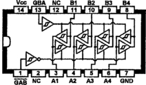
The three best known ‘74LS’-series bus transceiver ICs are the 74LS242, 74LS243, and 74LS245. The 74LS242 (inverting) and 74LS243 (non-inverting) ICs are 4-line transceivers with similar outlines and pin notations; Figure 14.27 shows the functional diagram of the 74LS243, which has a Function Table identical to that shown in Figure 14.26. The 74LS245 is an 8-line non-inverting transceiver that incorporates logic circuitry that makes it impossible for an ‘illegal’ input gating state to occur; this IC is housed in a 20-pin DIL package. These three ICs are also available in the ‘74HC’-series.
Using Open-drain Outputs
A small proportion of CMOS ICs have open-drain (o.d.) outputs. The cheapest IC of this type is the 40107B Dual 2-input NAND buffer/driver, which (in its popular 8-pin version) has the functional diagram shown in Figure 14.28, and is a useful device for demonstrating ‘open-drain’ basics. Note that each of this IC’s two basic ‘elements’ effectively consists of a 2-input AND gate with its output connected to the gate of an n-channel MOSFET, which has its drain connected directly to the OUT terminal. This element can be made to function as a 2-input NAND gate by connecting it as shown in Figure 14.29, with a load resistor RL connected between the supply rail and OUT, and with the output voltage taken from the OUT terminal.

Figure 14.28 Functional diagram of the 40107B Dual 2-input NAND buffer/driver with open-drain outputs (8-pin DIL version)

Each 40107B element can be made to act as a simple buffer/driver with an o.d. output by shorting its two inputs together, as shown in Figure 14.30; this simple element can be used in a variety of basic ways, as shown in Figures 14.31 and 14.32. Thus, the element can be used as a simple inverter by connecting it as shown in Figure 14.31(a), or as an inverting level shifter (which converts input switching levels of V+ (l) into output switching levels of V+ (2)) by connecting it as shown in Figure 14.31(b).


Figure 14.31 Basic ways of using a 40107B element as (a) an inverter or (b) an inverting level shifter

Figure 14.32(a) shows how a 40107B element can be used as a load driver that activates the load when the input is driven to logic-1; the output can sink load currents of up to 100mA when the element is powered from a 15V supply. Finally, Figure 14.32(b) shows how two basic elements can be connected in the basic ‘wired NOR’ gate configuration, in which the two IGFET outputs share a common load (RL) and the output is thus driven low when either input goes high; in practice, any number of basic elements can be wired in parallel in this fashion to make a wired NOR gate of any desired ‘input’ size.
Miscellaneous Digital IC Types
All of the most important basic types of current-production digital ICs have now been covered in this volume, but there are a still a few types that have not yet been mentioned, because they are obsolescent or obsolete and may only be found in older equipment, or are unduly expensive or hard to find, etc. Included among these are the following devices:
Parity generators/checkers.: Whenever a digital word is transmitted along a severely interference-prone communication link it is possible that the word may be so degraded that its code is changed from that transmitted. Parity generator/checker ICs offer a simple means of checking the truth of a word’s code, via an extra ‘parity’ bit; when the word is to be transmitted, the IC looks at the number of ‘1’s that it contains and (typically) adds an extra ‘1’ bit to it if the number is even, or an extra ‘0’ bit if the number is odd. When the word is received, the IC looks at it and its parity bit and checks them for compatibility (parity); if parity exists, the word is assumed to be pure, and is passed, but if parity does not exist the word is proved to be corrupt, and the receiver system may then request the retransmission of the original word. The parity-checking system is not fool-proof, but does offer a very high level of security.
The best known current-production TTL IC of this type is the 74180 9-bit (8 data bits plus 1 parity bit) parity generator/checker, which uses standard TTL technology. The best known current-production CMOS parity generator/checker ICs are the 40101B and 74HC280 9-bit (8 data bits plus 1 parity bit) and the 4531B 13-bit (12 data bits plus 1 parity bit) types. Each of these ICs can be used to check fewer than its maximum number of input bits by wiring half of the unwanted inputs high and the other half low, or can be used to check more than its maximum number of input bits by cascading appropriate numbers of ICs.
Rate multiplexers.: These are a special type of programmable divider, in which the divide-by value equals B/X, where X is a settable limited-range whole-number value and B is a fixed base number (usually 10, 16 or 64); thus, if B = 10 and X is set at 7, the IC will output seven pulses for every ten that are applied at the input and have a divide-by value of 1.4286; if X is stepped through numbers 1 to 9, the IC output will provide 1 to 9 output pulses for every ten input pulses, and have divide-by values that step through the values 10, 5, 3.333, 2.5, 2, 1.667, 1.4286, 1.25, and 1.111. ICs of this type are (or used to be) useful in performing arithmetic operations such as multiplication and division, and in A-to-D and D-to-A conversion, etc., but have now been generally superseded by more sophisticated types of LSI device. The best known CMOS IC of this type is the 4527B decade rate multiplier, which has a base number of 10 and can accept any ‘X’ number from 1 to 9 (set via a 4-bit address).
Voltage controlled oscillators (VCOs).: A VCO is a circuit that generates a good squarewave output waveform that has its operating frequency variable over a wide range via a DC input voltage. The two best known CMOS ICs that provide this action are the 4046B and 74HC4046 ‘phase-locked loop’ (PLL) ICs, and Chapter 9 shows various ways of using the VCO sections of these ICs. Chapter 15 shows some practical ways of using these ICs and their VCOs in the PLL mode.